Embed Size (px)
Citation preview
APPLICATION NOTE
R01AN1729EJ0110 Rev. 1.10 Page 1 of 15 July 1, 2014
M16C Family, RX Family Migrating From the M16C Family to the RX Family: Timers
Abstract This document describes migrating from timer A and timer B in the M16C Family to MTU2 in the RX Family.
Products M16C Family, RX Family
As an example of migrating from the M16C Family to the RX Family, the explanation in this document uses the RX210 Group in the RX Family and the M16C/65C Group in the M16C Family. When using this application note with other Renesas MCUs, careful evaluation is recommended after making modifications to comply with the alternate MCU. There are differences in the terminology between the M16C Family and RX Family. The table below lists the differences in terminology related to timers.
Differences in Terminology Item RX Family M16C Family
Timer modules
Multi-function timer pulse unit 2 (MTU2) Compare match timer (CMT) 16-bit timer pulse unit (TPU) 8-bit timer (TMR) Etc.
Timer A Timer B Etc.
Peripheral function operating clocks
Peripheral module clocks: PCLKA, PCLKB, PCLKC, PCLKD
Peripheral function clocks: fC, fC32, fOCO40M, fOCO-F, fOCO-S, f1
Timer operating clocks (hereinafter count clock) Count clock Count source
Function for selecting peripheral function input and output for pins
MPC *1 Function select registers and input function select registers *2
Registers for peripheral functions I/O registers SFRs
Note 1. The MPC is not available in some groups. Note 2. Only available in the M32C Group and R32C Group.
R01AN1729EJ0110 Rev. 1.10
July 1, 2014
M16C Family, RX Family Migrating From the M16C Family to the RX Family: Timers
R01AN1729EJ0110 Rev. 1.10 Page 2 of 15 July 1, 2014
Contents 1. Peripheral Functions Used ................................................................................................................. 3
1.1 Outputting a PWM Waveform ...................................................................................................... 3 1.2 One-Shot Timer ........................................................................................................................... 5 1.3 Measuring a Pulse Period ............................................................................................................ 8 1.4 Measuring a Pulse Width ........................................................................................................... 10
2. Related Sections in the RX User’s Manual: Hardware ..................................................................... 12
3. Appendix ........................................................................................................................................... 12 3.1 Points on Migrating From the M16C Family to the RX Family ................................................... 12
3.1.1 Interrupts ............................................................................................................................. 12 3.1.2 I/O Ports .............................................................................................................................. 13 3.1.3 Module Stop Function ......................................................................................................... 13
3.2 I/O Register Macros ................................................................................................................... 13 3.3 Intrinsic Functions ...................................................................................................................... 14
4. Reference Documents ...................................................................................................................... 15

M16C Family, RX Family Migrating From the M16C Family to the RX Family: Timers
R01AN1729EJ0110 Rev. 1.10 Page 3 of 15 July 1, 2014
1. Peripheral Functions Used This document describes an operating example when using MTU2 in the RX Family, and timer A and timer B in the M16C Family.
Table 1.1 lists the Peripheral Functions and Modes Used in Relation to the Operating Example. Table 1.1 Peripheral Functions and Modes Used in Relation to the Operating Example
No. Operation Mode Reference M16C RX 1 PWM output
Timer A PWM mode, timer mode (1)
MTU2
PWM1 mode Section 1.1
2 Single pulse output (one-shot timer) One-shot timer mode PWM1 mode Section 1.2
3 Frequency measurement of an input pulse Timer B
Pulse period measurement mode Normal mode Section 1.3
4 Width measurement of an input pulse
Pulse width measurement mode Normal mode Section 1.4
Note 1: In timer mode, only a pulse with a duty cycle of 50% can be output. 1.1 Outputting a PWM Waveform This section explains the differences of how a PWM waveform is output from an output pin using PWM1 mode of MTU2 in the RX Family and the timer mode of timer A in the M16C Family.
MTU2 in the RX Family has a free-running counter (hereinafter TCNT register). In PWM1 mode, a value is set to the TGR register, and when the values for the TGR register and TCNT register match (compare match occurs), output can be high, low, or inverted.
This section describes an example of a PWM waveform being output. A high is output when the TCNT register and TGRA register values match, and a low is output when the TCNT register and TGRB register values match. This example assumes a duty cycle of 50%, and the M16C uses timer mode and not PWM mode.
Using PWM1 mode of MTU2 as an example, by making the TGRA register and TGRB register values the same, a pulse can be output with a duty cycle of 0% or 100%. Because timer A in the M16C Family cannot output a pulse with a duty cycle of 100%, timer output is stopped, and control must be performed by ports.
Figure 1.1 shows Outputting a PWM Waveform.
Output pin
Count source
1 cycle of the count source
1 cycle of the count source ×(TA0 register value + 1)
1 cycle of the count source ×TGRA register value
1 cycle of the count source × TGRB register value
[2] Signal from output pin inverts when counter underflows
1 cycle of the count source ×(TA0 register value + 1)
[2] Compare match A occurs
[3] Compare match B occurs
[1] Count operation starts
HighLow
HighLow
M16C Family
RX Family
Output pin
[1] Count operation starts
Figure 1.1 Outputting a PWM Waveform

M16C Family, RX Family Migrating From the M16C Family to the RX Family: Timers
R01AN1729EJ0110 Rev. 1.10 Page 4 of 15 July 1, 2014
Table 1.2 lists the Outline for Outputting a PWM Waveform. Table 1.2 Outline for Outputting a PWM Waveform
Item M16C (M16C/65C Timer A) RX (RX210 MTU2) Operating mode Timer mode PWM mode 1
Operation overview
[1] Count starts – The count operation is started.
[2] Counter underflows – Each time the counter underflows, output from the pin is inverted.
[1] Count starts – The count operation is started.
[2] Compare match A occurs – When the TCNT and TGRA values match, compare match A occurs, and output from the pin changes from low to high.
[3] Compare match B occurs – When the TCNT and TGRB values match, compare match B occurs, and output from the pin changes from high to low. When compare match B occurs, the TCNT value is cleared.
Table 1.3 lists the Differences in Outputting a PWM Waveform. Table 1.3 Differences in Outputting a PWM Waveform
Step M16C (M16C/65C Timer A) RX (RX210 MTU2)
1 Cancel the module stop state *1 N/A (no module stop function)
SYSTEM.PRCR.WORD = 0xA502; MSTP(MTU) = 0; SYSTEM.PRCR.WORD = 0xA500;
2 Stop the count operation ta0s = 0; MTU.TSTR.BIT.CST0 = 0;
3 Operate the counter independently N/A (no processing) MTU.TSYR.BIT.SYNC0 = 0;
4 Clear the counter N/A (no processing) MTU0.TCNT = 0x0000;
5 Set the port to output a pulse *2 pd7_0 = 0;
PORTB.PDR.BIT.B3 = 0; PORTB.PMR.BIT.B3 = 0; MPC.PWPR.BIT.B0WI = 0; MPC.PWPR.BIT.PFSWE = 1; MPC.PB3PFS.BYTE = 0x01; MPC.PWPR.BYTE = 0x80; PORTB.PMR.BIT.B3 = 1;
6 Set the counter clock ta0mr = 0x84;
MTU0.TCR.BYTE = 0x42; 7 Set the operating mode MTU0.TMDR.BIT.MD = 2; 8 Set the I/O functions MTU0.TIORH.BYTE = 0x12;
9 Set the duty cycle and period ta0 = 0x80; MTU0.TGRA = 0x0800; MTU0.TGRB = 0x1000;
10 Start the count ta0s = 1; MTU.TSTR.BIT.CST0 = 1; Note 1. Refer to section 3.1.3 for details on the module stop function. Note 2. In the RX Family, pin settings for peripheral functions are configured in the MPC. Refer to section
3.1.2 for details.
M16C Family, RX Family Migrating From the M16C Family to the RX Family: Timers
R01AN1729EJ0110 Rev. 1.10 Page 5 of 15 July 1, 2014
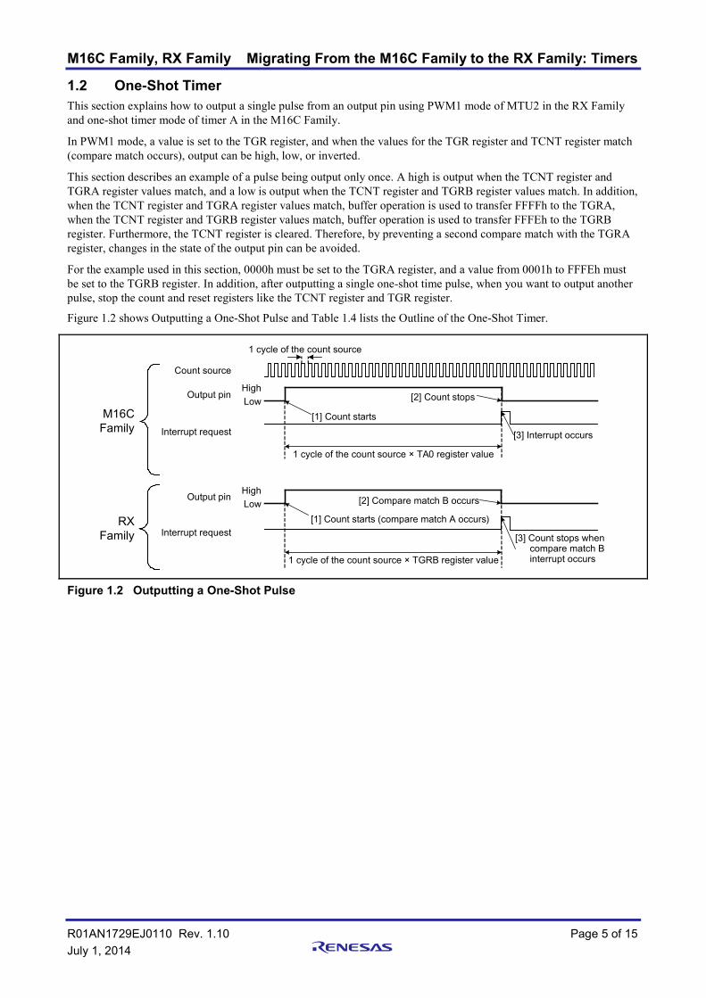
1.2 One-Shot Timer This section explains how to output a single pulse from an output pin using PWM1 mode of MTU2 in the RX Family and one-shot timer mode of timer A in the M16C Family.
In PWM1 mode, a value is set to the TGR register, and when the values for the TGR register and TCNT register match (compare match occurs), output can be high, low, or inverted.
This section describes an example of a pulse being output only once. A high is output when the TCNT register and TGRA register values match, and a low is output when the TCNT register and TGRB register values match. In addition, when the TCNT register and TGRA register values match, buffer operation is used to transfer FFFFh to the TGRA, when the TCNT register and TGRB register values match, buffer operation is used to transfer FFFEh to the TGRB register. Furthermore, the TCNT register is cleared. Therefore, by preventing a second compare match with the TGRA register, changes in the state of the output pin can be avoided.
For the example used in this section, 0000h must be set to the TGRA register, and a value from 0001h to FFFEh must be set to the TGRB register. In addition, after outputting a single one-shot time pulse, when you want to output another pulse, stop the count and reset registers like the TCNT register and TGR register.
Figure 1.2 shows Outputting a One-Shot Pulse and Table 1.4 lists the Outline of the One-Shot Timer.
1 cycle of the count source × TA0 register value
[2] Count stops
[1] Count starts
1 cycle of the count source × TGRB register value
[2] Compare match B occurs
[1] Count starts (compare match A occurs)
[3] Count stops when compare match B interrupt occurs
[3] Interrupt occurs
Output pinHigh
Count source
Interrupt request
Low
HighLow
M16C Family
RX Family
Output pin
Interrupt request
1 cycle of the count source
Figure 1.2 Outputting a One-Shot Pulse

M16C Family, RX Family Migrating From the M16C Family to the RX Family: Timers
R01AN1729EJ0110 Rev. 1.10 Page 6 of 15 July 1, 2014
Table 1.4 Outline of the One-Shot Timer Item M16C (M16C/65C Timer A) RX (RX210 MTU2)
Operating mode One-shot timer mode PWM mode 1
Operation overview
[1] Count starts – At the same time the count starts, the output pin changes from low to high.
[2] Count stops – When the TA0 count value becomes 0000h, the count stops, and the output pin changes from high to low.
[3] Interrupt occurs – A TA0 interrupt occurs when the TA0 register count becomes 0000h.
[1] Count starts (compare match A occurs) – When the TCNT and TGRA value match at the same time the count operation starts, compare match A occurs, and the output pin changes from low to high. Also, buffer operation is performed when compare match A occurs, and the value in TGRC (FFFF) is transferred to TGRA.
[2] Compare match B occurs – When the TCNT and TGRB values match, compare match B occurs, and output from the pin changes from high to low. Also, when compare match B occurs, the TCNT value is cleared, buffer operation is performed, and the value in TGRD (FFFF) is transferred to TGRB.
[3] Count stops when the compare match B interrupt occurs – The count stops by the compare match B interrupt handling program.
M16C Family, RX Family Migrating From the M16C Family to the RX Family: Timers
R01AN1729EJ0110 Rev. 1.10 Page 7 of 15 July 1, 2014
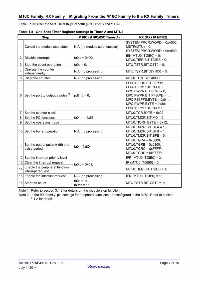
Table 1.5 lists the One-Shot Timer Register Settings in Timer A and MTU2. Table 1.5 One-Shot Timer Register Settings in Timer A and MTU2
Step M16C (M16C/65C Timer A) RX (RX210 MTU2)
1 Cancel the module stop state *1 N/A (no module stop function) SYSTEM.PRCR.WORD = 0xA502; MSTP(MTU) = 0; SYSTEM.PRCR.WORD = 0xA500;
2 Disable interrupts ta0ic = 0x00; IEN(MTU0, TGIB0) = 0; MTU0.TIER.BIT.TGIEB = 0;
3 Stop the count operation ta0s = 0; MTU.TSTR.BIT.CST0 = 0;
4 Operate the counter independently N/A (no processing) MTU.TSYR.BIT.SYNC0 = 0;
5 Clear the counter N/A (no processing) MTU0.TCNT = 0x0000;
6 Set the port to output a pulse *2 pd7_0 = 0;
PORTB.PDR.BIT.B3 = 0; PORTB.PMR.BIT.B3 = 0; MPC.PWPR.BIT.B0WI = 0; MPC.PWPR.BIT.PFSWE = 1; MPC.PB3PFS.BYTE = 0x01; MPC.PWPR.BYTE = 0x80; PORTB.PMR.BIT.B3 = 1;
7 Set the counter clock ta0mr = 0x86;
MTU0.TCR.BYTE = 0x02; 8 Set the I/O functions MTU0.TMDR.BIT.MD = 2; 9 Set the operating mode MTU0.TIORH.BYTE = 0x12;
10 Set the buffer operation N/A (no processing) MTU0.TMDR.BIT.BFA = 1; MTU0.TMDR.BIT.BFB = 1; MTU0.TMDR.BIT.BFE = 0;
11 Set the output pulse width and pulse period ta0 = 0x80;
MTU0.TGRA = 0x0000; MTU0.TGRB = 0c0800; MTU0.TGRC = 0xFFFF; MTU0.TGRD = 0xFFFE;
12 Set the interrupt priority level
ta0ic = 0x01;
IPR (MTU0, TGIB0) = 3; 13 Clear the interrupt request IR (MTU0, TGIB0) = 0;
14 Enable the peripheral function interrupt request MTU0.TIER.BIT.TGIEB = 1;
15 Enable the interrupt request N/A (no processing) IEN (MTU0, TGIB0) = 1;
16 Start the count ta0s = 1; ta0os = 1; MTU.TSTR.BIT.CST0 = 1;
Note 1. Refer to section 3.1.3 for details on the module stop function. Note 2. In the RX Family, pin settings for peripheral functions are configured in the MPC. Refer to section
3.1.2 for details.
M16C Family, RX Family Migrating From the M16C Family to the RX Family: Timers
R01AN1729EJ0110 Rev. 1.10 Page 8 of 15 July 1, 2014
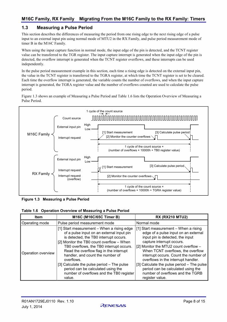
1.3 Measuring a Pulse Period This section describes the differences of measuring the period from one rising edge to the next rising edge of a pulse input to an external input pin using normal mode of MTU2 in the RX Family, and pulse period measurement mode of timer B in the M16C Family.
When using the input capture function in normal mode, the input edge of the pin is detected, and the TCNT register value can be transferred to the TGR register. The input capture interrupt is generated when the input edge of the pin is detected, the overflow interrupt is generated when the TCNT register overflows, and these interrupts can be used independently.
In the pulse period measurement example in this section, each time a rising edge is detected on the external input pin, the value in the TCNT register is transferred to the TGRA register, at which time the TCNT register is set to be cleared. Each time the overflow interrupt is generated, the variable counts the number of overflows, and when the input capture interrupt is generated, the TGRA register value and the number of overflows counted are used to calculate the pulse period.
Figure 1.3 shows an example of Measuring a Pulse Period and Table 1.6 lists the Operation Overview of Measuring a Pulse Period.
External input pinHigh
Count source
1 cycle of the count source
1 cycle of the count source ×(number of overflows × 10000h + TB0 register value)
Interrupt request
[1] Start measurement [3] Calculate pulse period[2] Monitor the counter overflows
1 cycle of the count source ×(number of overflows × 10000h + TGRA register value)
Interrupt request(overflow)
Low
[1] Start measurement
[2] Monitor the counter overflows
[3] Calculate pulse period
HighLow
M16C Family
RX Family
External input pin
Interrupt request
Figure 1.3 Measuring a Pulse Period
Table 1.6 Operation Overview of Measuring a Pulse Period
Item M16C (M16C/65C Timer B) RX (RX210 MTU2) Operating mode Pulse period measurement mode Normal mode
Operation overview
[1] Start measurement – When a rising edge of a pulse input on an external input pin is detected, the TB0 interrupt occurs.
[2] Monitor the TB0 count overflow – When TB0 overflows, the TB0 interrupt occurs. Read the overflow flag in the interrupt handler, and count the number of overflows.
[3] Calculate the pulse period – The pulse period can be calculated using the number of overflows and the TB0 register value.
[1] Start measurement – When a rising edge of a pulse input on an external input pin is detected, the input capture interrupt occurs.
[2] Monitor the MTU2 count overflow – When TCNT overflows, the overflow interrupt occurs. Count the number of overflows in the interrupt handler.
[3] Calculate the pulse period – The pulse period can be calculated using the number of overflows and the TGRB register value.
M16C Family, RX Family Migrating From the M16C Family to the RX Family: Timers
R01AN1729EJ0110 Rev. 1.10 Page 9 of 15 July 1, 2014
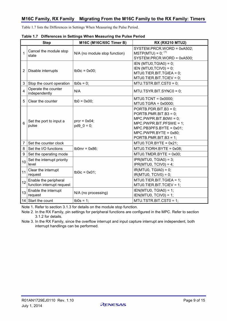
Table 1.7 lists the Differences in Settings When Measuring the Pulse Period. Table 1.7 Differences in Settings When Measuring the Pulse Period
Step M16C (M16C/65C Timer B) RX (RX210 MTU2)
1 Cancel the module stop state N/A (no module stop function)
SYSTEM.PRCR.WORD = 0xA502; MSTP(MTU) = 0; (1) SYSTEM.PRCR.WORD = 0xA500;
2 Disable interrupts tb0ic = 0x00;
IEN (MTU0,TGIA0) = 0; IEN (MTU0,TCIV0) = 0; MTU0.TIER.BIT.TGIEA = 0; MTU0.TIER.BIT.TCIEV = 0;
3 Stop the count operation tb0s = 0; MTU.TSTR.BIT.CST0 = 0;
4 Operate the counter independently N/A MTU.TSYR.BIT.SYNC0 = 0;
5 Clear the counter tb0 = 0x00; MTU0.TCNT = 0x0000; MTU0.TGRA = 0x0000;
6 Set the port to input a pulse
prcr = 0x04; pd9_0 = 0;
PORTB.PDR.BIT.B3 = 0; PORTB.PMR.BIT.B3 = 0; MPC.PWPR.BIT.B0WI = 0; MPC.PWPR.BIT.PFSWE = 1; MPC.PB3PFS.BYTE = 0x01; MPC.PWPR.BYTE = 0x80; PORTB.PMR.BIT.B3 = 1;
7 Set the counter clock tb0mr = 0x86;
MTU0.TCR.BYTE = 0x21; 8 Set the I/O functions MTU0.TIORH.BYTE = 0x08; 9 Set the operating mode MTU0.TMDR.BYTE = 0x00;
10 Set the interrupt priority level
tb0ic = 0x01;
IPR(MTU0, TGIA0) = 3; IPR(MTU0, TCIV0) = 4;
11 Clear the interrupt request
IR(MTU0, TGIA0) = 0; IR(MTU0, TCIV0) = 0;
12 Enable the peripheral function interrupt request
MTU0.TIER.BIT.TGIEA = 1; MTU0.TIER.BIT.TCIEV = 1;
13 Enable the interrupt request N/A (no processing) IEN(MTU0, TGIA0) = 1;
IEN(MTU0, TCIV0) = 1; 14 Start the count tb0s = 1; MTU.TSTR.BIT.CST0 = 1; Note 1. Refer to section 3.1.3 for details on the module stop function. Note 2. In the RX Family, pin settings for peripheral functions are configured in the MPC. Refer to section
3.1.2 for details. Note 3. In the RX Family, since the overflow interrupt and input capture interrupt are independent, both
interrupt handlings can be performed.

M16C Family, RX Family Migrating From the M16C Family to the RX Family: Timers
R01AN1729EJ0110 Rev. 1.10 Page 10 of 15 July 1, 2014
1.4 Measuring a Pulse Width This section describes the differences of measuring the pulse width from one rising edge to the next falling edge of a pulse input to an external input pin using normal mode of MTU2 in the RX Family, and pulse width measurement mode of timer B in the M16C Family.
When using the input capture function in normal mode, the input edge of the pin is detected, and the TCNT register value can be transferred to the TGR register. The input capture interrupt is generated when the input edge of the pin is detected, the overflow interrupt is generated when the TCNT register overflows, and these interrupts can be used independently.
In the pulse width measurement example in this section, each time an edge is detected (rising edge or falling edge) on the external input pin, the value in the TCNT register is transferred to the TGRA register, at which time the TCNT register is set to be cleared. Each time the overflow interrupt is generated, the variable counts the number of overflows, and when the input capture interrupt is generated, the TGRA register value and the number of overflows counted are used to calculate the pulse width.
Figure 1.4 shows an example of Pulse Width Measurement and Table 1.8 lists the Operation Overview of Measuring a Pulse Width.
1 cycles of the count source ×(number of overflows × 10000h + TBi register value)
[1] Measurement starts [3] Pulse width calculated
[2] Count overflow monitored
1 cycle of the count source ×(number of overflows × 10000h + TGR register value)
[3] Pulse width calculated[1] Measurement starts
[2] Count overflow monitored
External input pinHigh
Count source
1 cycle of the count source
Interrupt request
Interrupt request(overflow)
Low
HighLow
M16C Family
RX Family
External input pin
Interrupt request
Figure 1.4 Measuring a Pulse Width
Table 1.8 Operation Overview of Measuring a Pulse Width Item M16C (M16C/65C Timer B) RX (RX210 MTU2)
Operating mode Pulse width measurement mode Normal mode
Operation overview
[1] Measurement starts – When a rising edge or falling edge of a pulse input on an external input pin is detected, the TB0 interrupt occurs.
[2] Count overflow monitored – When TB0 overflows, the TB0 interrupt occurs. Read the overflow flag in the interrupt handler, and count the number of overflows.
[3] Pulse width calculated – The pulse width can be calculated using the number of overflows and the TB0 register value.
[1] Measurement starts – When a rising edge or falling edge of a pulse input on an external input pin is detected, the input capture interrupt occurs.
[2] Count overflow monitored – When TCNT overflows, the overflow interrupt occurs. Count the number of overflows in the interrupt handler.
[3] Pulse width calculated – The pulse width can be calculated using the number of overflows and the TGR register value.
M16C Family, RX Family Migrating From the M16C Family to the RX Family: Timers
R01AN1729EJ0110 Rev. 1.10 Page 11 of 15 July 1, 2014
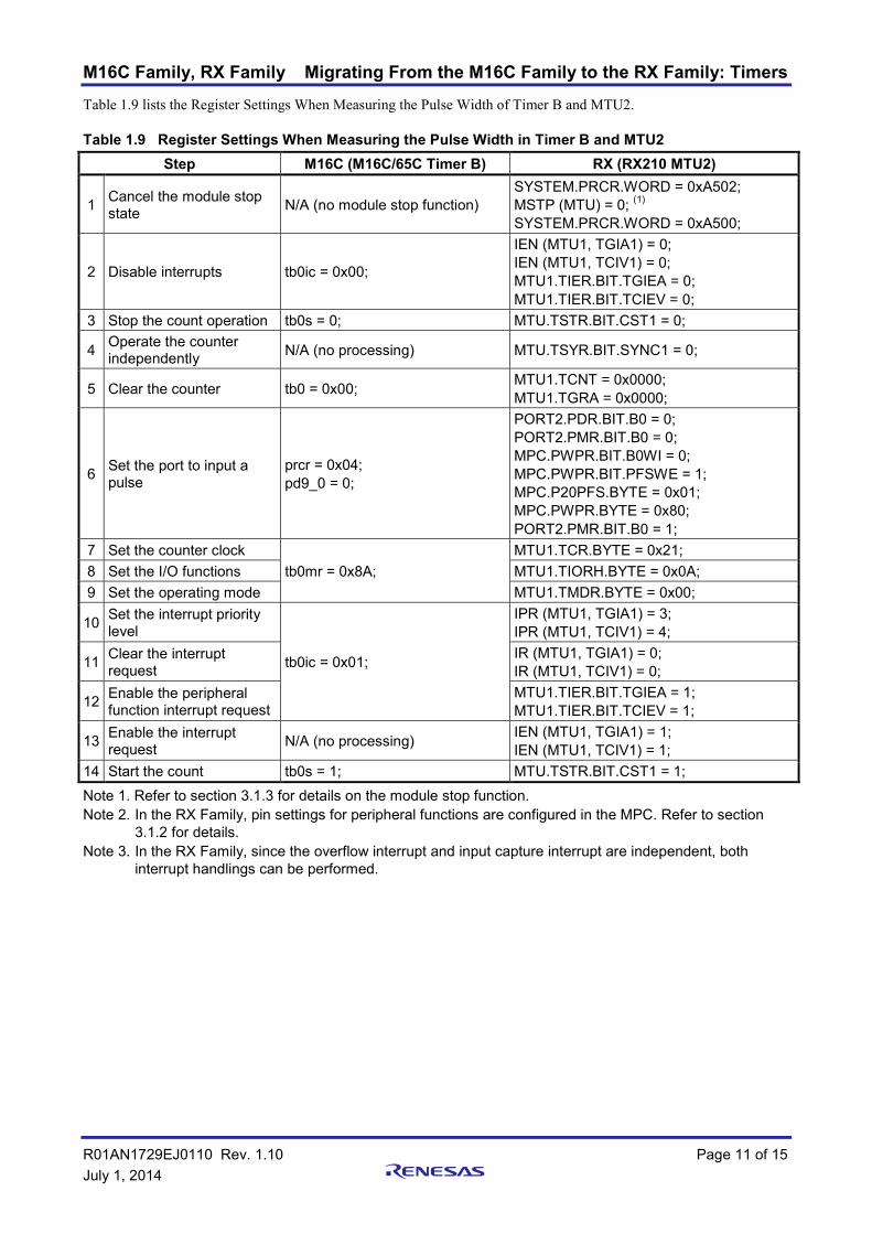
Table 1.9 lists the Register Settings When Measuring the Pulse Width of Timer B and MTU2. Table 1.9 Register Settings When Measuring the Pulse Width in Timer B and MTU2
Step M16C (M16C/65C Timer B) RX (RX210 MTU2)
1 Cancel the module stop state N/A (no module stop function)
SYSTEM.PRCR.WORD = 0xA502; MSTP (MTU) = 0; (1) SYSTEM.PRCR.WORD = 0xA500;
2 Disable interrupts tb0ic = 0x00;
IEN (MTU1, TGIA1) = 0; IEN (MTU1, TCIV1) = 0; MTU1.TIER.BIT.TGIEA = 0; MTU1.TIER.BIT.TCIEV = 0;
3 Stop the count operation tb0s = 0; MTU.TSTR.BIT.CST1 = 0;
4 Operate the counter independently N/A (no processing) MTU.TSYR.BIT.SYNC1 = 0;
5 Clear the counter tb0 = 0x00; MTU1.TCNT = 0x0000; MTU1.TGRA = 0x0000;
6 Set the port to input a pulse
prcr = 0x04; pd9_0 = 0;
PORT2.PDR.BIT.B0 = 0; PORT2.PMR.BIT.B0 = 0; MPC.PWPR.BIT.B0WI = 0; MPC.PWPR.BIT.PFSWE = 1; MPC.P20PFS.BYTE = 0x01; MPC.PWPR.BYTE = 0x80; PORT2.PMR.BIT.B0 = 1;
7 Set the counter clock tb0mr = 0x8A;
MTU1.TCR.BYTE = 0x21; 8 Set the I/O functions MTU1.TIORH.BYTE = 0x0A; 9 Set the operating mode MTU1.TMDR.BYTE = 0x00;
10 Set the interrupt priority level
tb0ic = 0x01;
IPR (MTU1, TGIA1) = 3; IPR (MTU1, TCIV1) = 4;
11 Clear the interrupt request
IR (MTU1, TGIA1) = 0; IR (MTU1, TCIV1) = 0;
12 Enable the peripheral function interrupt request
MTU1.TIER.BIT.TGIEA = 1; MTU1.TIER.BIT.TCIEV = 1;
13 Enable the interrupt request N/A (no processing) IEN (MTU1, TGIA1) = 1;
IEN (MTU1, TCIV1) = 1; 14 Start the count tb0s = 1; MTU.TSTR.BIT.CST1 = 1; Note 1. Refer to section 3.1.3 for details on the module stop function. Note 2. In the RX Family, pin settings for peripheral functions are configured in the MPC. Refer to section
3.1.2 for details. Note 3. In the RX Family, since the overflow interrupt and input capture interrupt are independent, both
interrupt handlings can be performed.
M16C Family, RX Family Migrating From the M16C Family to the RX Family: Timers
R01AN1729EJ0110 Rev. 1.10 Page 12 of 15 July 1, 2014
2. Related Sections in the RX User’s Manual: Hardware When migrating from the M16C Family to the RX Family, refer to the following sections of the RX User’s Manual: Hardware.
Multi-Function Timer Pulse Unit 2 Clock Generation Circuit Low Power Consumption Interrupt Controller, CPU I/O Ports, MPC Register Write Protection Function
3. Appendix
3.1 Points on Migrating From the M16C Family to the RX Family This chapter explains points on migrating from the M16C Family to the RX Family. 3.1.1 Interrupts For the RX Family, when an interrupt request is received while all of the following conditions are met, the interrupt occurs. The I flag (PSW.I bit) is 1. Registers IER and IPR in the ICU are set to interrupt enabled. The interrupt request enable bit for peripheral functions is enabled.
Table 3.1 lists a Comparison of Conditions for Interrupt Generation.
Table 3.1 Comparison of Conditions for Interrupt Generation Item M16C/65C RX210
I flag When the I flag is set to 1 (enabled), the interrupt request is accepted.
Interrupt request flag When there is an interrupt request from a peripheral function, the interrupt request flag becomes 1 (interrupt requested).
Interrupt priority level Selected by setting bits ILVL2 to ILVL0. Selected by setting the IPR[3:0] bits. Interrupt request enable N/A Specified by setting the IER register. Interrupt enable for peripheral functions N/A Interrupts can be enabled or disabled in
each peripheral function.
For more information, refer to sections Interrupt Controller (ICU), CPU, and sections for other peripheral functions used in the User’s Manual: Hardware.

M16C Family, RX Family Migrating From the M16C Family to the RX Family: Timers
R01AN1729EJ0110 Rev. 1.10 Page 13 of 15 July 1, 2014
3.1.2 I/O Ports In the RX Family, the MPC must be configured in order to assign I/O signals from peripheral functions to pins. Before controlling the input and output pins in the RX Family, the following two items must be set. In the MPC.PFS register, select the peripheral functions that are assigned to the appropriate pins. In the PORTn.PMR register, select an appropriate pin to be used as a general I/O port or I/O port for a peripheral
function.
Table 3.2 lists a Comparison of I/O Settings for Peripheral Function Pins.
Table 3.2 Comparison of I/O Settings for Peripheral Function Pins Function M16C/65C RX210
Select the pin function These are not available in the M16C Family. *1 When a mode is set for a peripheral function, appropriate pins are assigned as I/O pins for the peripheral function.
With the PFS register, I/O ports for peripheral functions can be assigned by selecting from multiple pins.
Switch between general I/O port and peripheral function
With the PMR register, the corresponding pin function can be selected as a general I/O port or a peripheral function.
Note 1. Register for similar functions are available in the M32C Group and R32C Group. For more information, refer to the Multi-Function Pin Controller (MPC) and I/O port sections in the User’s Manual: Hardware.
3.1.3 Module Stop Function The RX Family has the ability to stop each peripheral module individually. By transitioning unused peripheral modules to the module stop state, power consumption can be reduced. After the reset is released, all modules (with a few exceptions) are in the module stop state. Registers for modules in the module stop state cannot be read or write accessed.
For more information, refer to the Low Power Consumption section in the User’s Manual: Hardware.
3.2 I/O Register Macros Macro definitions listed in Table 3.4 can be found in the RX I/O register definitions (iodefine.h).
The readability of programs can be achieved with these macro definitions.
Table 3.4 lists examples of macros.
Table 3.3 Using Macros Macro Usage Example
IR("module name", "bit name") IR(MTU0,TGIA0) = 0 ; The IR bit corresponding to MTU0.TGIA0 is cleared to 0 (no interrupt request is generated).
IEN("module name", "bit name") IEN(MTU0, TGIA0) = 1 ; The IEN bit corresponding to MTU0.TGIA0 is set to 1 (interrupt request enabled).
IPR("module name", "bit name") IPR(MTU0, TGIA0) = 0x02 ; The IPR[3:0] bits corresponding to MTU0.TGIA0 are set to 0010b (interrupt priority level 2).
MSTP("module name") MSTP(MTU) = 0 ; The MTU0 Module Stop bit is set to 0 (module stop state is canceled).
VECT("module name", "bit name") #pragma interrupt(Excep_MTU0_TGIA0 (vect=VECT(MTU0, TGIA0)) The interrupt function is declared for the corresponding MTU0.TGIA0 register.

M16C Family, RX Family Migrating From the M16C Family to the RX Family: Timers
R01AN1729EJ0110 Rev. 1.10 Page 14 of 15 July 1, 2014
3.3 Intrinsic Functions The RX Family has intrinsic functions for setting control registers and special instructions. When using intrinsic functions, include machine.h.
Table 3.4 lists examples of Descriptions of Special Instructions and Control Register Settings. Table 3.4 Descriptions of Special Instructions and Control Register Settings
Item Description
RX M16C Set the I flag to 1 setpsw_i (); *1 asm("fset i"); Set the I flag to 0 clrpsw_i (); *1 asm("fclr i"); Expanded into the WAIT instruction wait(); *1 asm("wait"); Expanded into the NOP instruction nop(); *1 asm("nop");
Note 1. "machine.h" must be included.

M16C Family, RX Family Migrating From the M16C Family to the RX Family: Timers
R01AN1729EJ0110 Rev. 1.10 Page 15 of 15 July 1, 2014
4. Reference Documents User’s Manual: Hardware
RX210 Group User's Manual: Hardware Rev.1.50 (R01UH0037EJ) M16C/65C Group User's Manual: Hardware Rev.1.10 (R01UH0093) Refer to the corresponding UMH when using products other than the RX210 Group and M16C/65C Group. The latest versions can be downloaded from the Renesas Electronics website.
Technical Update/Technical News
The latest information can be downloaded from the Renesas Electronics website. User’s Manual: Development Tools
RX Family C/C++ Compiler Package V.1.01 User's Manual Rev.1.00 (R20UT0570EJ) M16C Series, R8C Family C Compiler Package V5.45 C Compiler User's Manual Rev.3.00 The latest versions can be downloaded from the Renesas Electronics website.
Website and Support Renesas Electronics website
http://www.renesas.com Inquiries
http://www.renesas.com/contact/
A-1
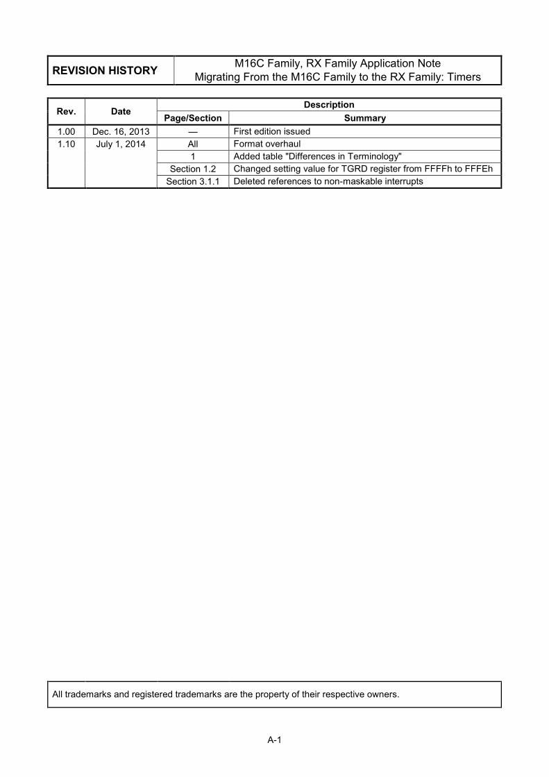
REVISION HISTORY M16C Family, RX Family Application Note Migrating From the M16C Family to the RX Family: Timers
Rev. Date Description
Page/Section Summary 1.00 Dec. 16, 2013 — First edition issued 1.10 July 1, 2014 All Format overhaul
1 Added table "Differences in Terminology" Section 1.2 Changed setting value for TGRD register from FFFFh to FFFEh
Section 3.1.1 Deleted references to non-maskable interrupts
All trademarks and registered trademarks are the property of their respective owners.

General Precautions in the Handling of MPU/MCU Products The following usage notes are applicable to all MPU/MCU products from Renesas. For detailed usage notes on the products covered by this document, refer to the relevant sections of the document as well as any technical updates that have been issued for the products.
1. Handling of Unused Pins
Handle unused pins in accordance with the directions given under Handling of Unused Pins in the manual.
⎯ The input pins of CMOS products are generally in the high-impedance state. In operation with an unused pin in the open-circuit state, extra electromagnetic noise is induced in the vicinity of LSI, an associated shoot-through current flows internally, and malfunctions occur due to the false recognition of the pin state as an input signal become possible. Unused pins should be handled as described under Handling of Unused Pins in the manual.
2. Processing at Power-on
The state of the product is undefined at the moment when power is supplied.
⎯ The states of internal circuits in the LSI are indeterminate and the states of register settings and pins are undefined at the moment when power is supplied. In a finished product where the reset signal is applied to the external reset pin, the states of pins are not guaranteed from the moment when power is supplied until the reset process is completed. In a similar way, the states of pins in a product that is reset by an on-chip power-on reset function are not guaranteed from the moment when power is supplied until the power reaches the level at which resetting has been specified.
3. Prohibition of Access to Reserved Addresses
Access to reserved addresses is prohibited.
⎯ The reserved addresses are provided for the possible future expansion of functions. Do not access these addresses; the correct operation of LSI is not guaranteed if they are accessed.
4. Clock Signals
After applying a reset, only release the reset line after the operating clock signal has become stable. When switching the clock signal during program execution, wait until the target clock signal has stabilized.
⎯ When the clock signal is generated with an external resonator (or from an external oscillator) during a reset, ensure that the reset line is only released after full stabilization of the clock signal. Moreover, when switching to a clock signal produced with an external resonator (or by an external oscillator) while program execution is in progress, wait until the target clock signal is stable.
5. Differences between Products
Before changing from one product to another, i.e. to a product with a different part number, confirm that the change will not lead to problems.
⎯ The characteristics of an MPU or MCU in the same group but having a different part number may differ in terms of the internal memory capacity, layout pattern, and other factors, which can affect the ranges of electrical characteristics, such as characteristic values, operating margins, immunity to noise, and amount of radiated noise. When changing to a product with a different part number, implement a system-evaluation test for the given product.
Notice1. Descriptions of circuits, software and other related information in this document are provided only to illustrate the operation of semiconductor products and application examples. You are fully responsible for
the incorporation of these circuits, software, and information in the design of your equipment. Renesas Electronics assumes no responsibility for any losses incurred by you or third parties arising from the
use of these circuits, software, or information.
2. Renesas Electronics has used reasonable care in preparing the information included in this document, but Renesas Electronics does not warrant that such information is error free. Renesas Electronics
assumes no liability whatsoever for any damages incurred by you resulting from errors in or omissions from the information included herein.
3. Renesas Electronics does not assume any liability for infringement of patents, copyrights, or other intellectual property rights of third parties by or arising from the use of Renesas Electronics products or
technical information described in this document. No license, express, implied or otherwise, is granted hereby under any patents, copyrights or other intellectual property rights of Renesas Electronics or
others.
4. You should not alter, modify, copy, or otherwise misappropriate any Renesas Electronics product, whether in whole or in part. Renesas Electronics assumes no responsibility for any losses incurred by you or
third parties arising from such alteration, modification, copy or otherwise misappropriation of Renesas Electronics product.
5. Renesas Electronics products are classified according to the following two quality grades: "Standard" and "High Quality". The recommended applications for each Renesas Electronics product depends on
the product's quality grade, as indicated below.
"Standard": Computers; office equipment; communications equipment; test and measurement equipment; audio and visual equipment; home electronic appliances; machine tools; personal electronic
equipment; and industrial robots etc.
"High Quality": Transportation equipment (automobiles, trains, ships, etc.); traffic control systems; anti-disaster systems; anti-crime systems; and safety equipment etc.
Renesas Electronics products are neither intended nor authorized for use in products or systems that may pose a direct threat to human life or bodily injury (artificial life support devices or systems, surgical
implantations etc.), or may cause serious property damages (nuclear reactor control systems, military equipment etc.). You must check the quality grade of each Renesas Electronics product before using it
in a particular application. You may not use any Renesas Electronics product for any application for which it is not intended. Renesas Electronics shall not be in any way liable for any damages or losses
incurred by you or third parties arising from the use of any Renesas Electronics product for which the product is not intended by Renesas Electronics.
6. You should use the Renesas Electronics products described in this document within the range specified by Renesas Electronics, especially with respect to the maximum rating, operating supply voltage
range, movement power voltage range, heat radiation characteristics, installation and other product characteristics. Renesas Electronics shall have no liability for malfunctions or damages arising out of the
use of Renesas Electronics products beyond such specified ranges.
7. Although Renesas Electronics endeavors to improve the quality and reliability of its products, semiconductor products have specific characteristics such as the occurrence of failure at a certain rate and
malfunctions under certain use conditions. Further, Renesas Electronics products are not subject to radiation resistance design. Please be sure to implement safety measures to guard them against the
possibility of physical injury, and injury or damage caused by fire in the event of the failure of a Renesas Electronics product, such as safety design for hardware and software including but not limited to
redundancy, fire control and malfunction prevention, appropriate treatment for aging degradation or any other appropriate measures. Because the evaluation of microcomputer software alone is very difficult,
please evaluate the safety of the final products or systems manufactured by you.
8. Please contact a Renesas Electronics sales office for details as to environmental matters such as the environmental compatibility of each Renesas Electronics product. Please use Renesas Electronics
products in compliance with all applicable laws and regulations that regulate the inclusion or use of controlled substances, including without limitation, the EU RoHS Directive. Renesas Electronics assumes
no liability for damages or losses occurring as a result of your noncompliance with applicable laws and regulations.
9. Renesas Electronics products and technology may not be used for or incorporated into any products or systems whose manufacture, use, or sale is prohibited under any applicable domestic or foreign laws or
regulations. You should not use Renesas Electronics products or technology described in this document for any purpose relating to military applications or use by the military, including but not limited to the
development of weapons of mass destruction. When exporting the Renesas Electronics products or technology described in this document, you should comply with the applicable export control laws and
regulations and follow the procedures required by such laws and regulations.
10. It is the responsibility of the buyer or distributor of Renesas Electronics products, who distributes, disposes of, or otherwise places the product with a third party, to notify such third party in advance of the
contents and conditions set forth in this document, Renesas Electronics assumes no responsibility for any losses incurred by you or third parties as a result of unauthorized use of Renesas Electronics
products.
11. This document may not be reproduced or duplicated in any form, in whole or in part, without prior written consent of Renesas Electronics.
12. Please contact a Renesas Electronics sales office if you have any questions regarding the information contained in this document or Renesas Electronics products, or if you have any other inquiries.
(Note 1) "Renesas Electronics" as used in this document means Renesas Electronics Corporation and also includes its majority-owned subsidiaries.
(Note 2) "Renesas Electronics product(s)" means any product developed or manufactured by or for Renesas Electronics.
http://www.renesas.comRefer to "http://www.renesas.com/" for the latest and detailed information.
Renesas Electronics America Inc.2801 Scott Boulevard Santa Clara, CA 95050-2549, U.S.A.Tel: +1-408-588-6000, Fax: +1-408-588-6130Renesas Electronics Canada Limited1101 Nicholson Road, Newmarket, Ontario L3Y 9C3, CanadaTel: +1-905-898-5441, Fax: +1-905-898-3220Renesas Electronics Europe LimitedDukes Meadow, Millboard Road, Bourne End, Buckinghamshire, SL8 5FH, U.KTel: +44-1628-585-100, Fax: +44-1628-585-900Renesas Electronics Europe GmbHArcadiastrasse 10, 40472 Düsseldorf, Germany Tel: +49-211-6503-0, Fax: +49-211-6503-1327Renesas Electronics (China) Co., Ltd.Room 1709, Quantum Plaza, No.27 ZhiChunLu Haidian District, Beijing 100191, P.R.ChinaTel: +86-10-8235-1155, Fax: +86-10-8235-7679Renesas Electronics (Shanghai) Co., Ltd.Unit 301, Tower A, Central Towers, 555 Langao Road, Putuo District, Shanghai, P. R. China 200333 Tel: +86-21-2226-0888, Fax: +86-21-2226-0999Renesas Electronics Hong Kong LimitedUnit 1601-1613, 16/F., Tower 2, Grand Century Place, 193 Prince Edward Road West, Mongkok, Kowloon, Hong KongTel: +852-2265-6688, Fax: +852 2886-9022/9044Renesas Electronics Taiwan Co., Ltd.13F, No. 363, Fu Shing North Road, Taipei 10543, TaiwanTel: +886-2-8175-9600, Fax: +886 2-8175-9670Renesas Electronics Singapore Pte. Ltd.80 Bendemeer Road, Unit #06-02 Hyflux Innovation Centre, Singapore 339949Tel: +65-6213-0200, Fax: +65-6213-0300Renesas Electronics Malaysia Sdn.Bhd.Unit 906, Block B, Menara Amcorp, Amcorp Trade Centre, No. 18, Jln Persiaran Barat, 46050 Petaling Jaya, Selangor Darul Ehsan, MalaysiaTel: +60-3-7955-9390, Fax: +60-3-7955-9510Renesas Electronics Korea Co., Ltd.12F., 234 Teheran-ro, Gangnam-Ku, Seoul, 135-920, KoreaTel: +82-2-558-3737, Fax: +82-2-558-5141
SALES OFFICES
© 2014 Renesas Electronics Corporation. All rights reserved.Colophon 4.0