Embed Size (px)
Citation preview

M. FOUAIDY Thin films applied to superconducting RF cavities Legnaro Oct.10, 2006
An alternative device, for Nb/Cu samples RF properties characterization purpose was developed. The main feature of this technique, which is based on thermometry, is an improved accuracy and sensitivity as compared to the improved accuracy and sensitivity as compared to the usual RF methodusual RF method. The thermometric method, conjointly with a thermal model, is used for the measurement of the absolute RS distributionRS distribution on superconducting thin film samples. Precise calibration of test-samples RF losses is performed by means of a removable DC heater and temperature sensors pressed on the back of the disk and placed in a vacuum chamber. This new facility allows in-situ determination of all the thermal parameters involved in the model (substrate thermal conductivity and heat transfer coefficient at the solid-Lhe interface). The thermometric technique was first successfully validated and RF properties of several Nb/Cu sample was studiedvalidated and RF properties of several Nb/Cu sample was studied with this new device. Interesting data was obtained and analyzed. In particular, the effect of effect of the copper substrate surfacethe copper substrate surface conditions on the Nb/Cu sample RF propertiesNb/Cu sample RF properties was investigated and the corresponding results discussed.
Determination of Niobium films surface resistance by a calorimetric method
M. Fouaidy, IPN Orsay, France P. Bosland, M. Ribeaudeau, S. Chel, J.P. Charrier, CEA Saclay, France

M. FOUAIDY Thin films applied to superconducting RF cavities Legnaro Oct.10, 2006
TOPICS
Motivation for developing such an instrument
Purpose
Main advantages of the calorimetric method
Method principle and thermal modelling
Thermometric system
Measured versus simulated temperature profiles
Sensitivity and accuracy of the calorimetric
method
Validation of the calorimetric method
Test results with sputtered niobium films

M. FOUAIDY Thin films applied to superconducting RF cavities Legnaro Oct.10, 2006
Why did we need to develop a new instrument for measuring the
RF surface resistance (Rs) of sputtered superconducting films with
such SRF cavity ?
Improve accuracy and sensitivity of Rs measurement,
Lack of accuracy and sensitivity at 4.2 K for measurements
performed by the end plate replacement method !
Measure exclusively the test-sample RF losses by excluding
any
extra RF losses :
Some of extra RF losses are inherent to the ‘classical’ method
(rest of the cavity, indium gasket, RF coupling loops)
Potentially, anomalous RF losses induced by Field Emitted
electron impacting area other than the sample
Motivations for developing such an instrument
M. FOUAIDY Thin films applied to superconducting RF cavities Legnaro Oct.10, 2006
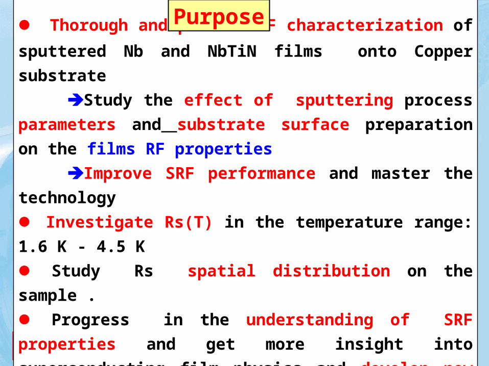
Improve accuracy, reliability and sensitivity of Rs
measurement
Thorough and precise RF characterization of sputtered Nb
and NbTiN films onto Copper substrate
Study the effect of sputtering process parameters and
substrate surface preparation on the films RF properties
Improve SRF performance and master the technology
Investigate Rs(T) in the temperature range: 1.6 K - 4.5 K
Study Rs spatial distribution on the sample .
Progress in the understanding of SRF properties and get
more insight into superconducting film physics and develop new
superconducting material interesting for accelerators
Purpose

M. FOUAIDY Thin films applied to superconducting RF cavities Legnaro Oct.10, 2006
Absolute, direct and local method as compared to the usual
RF technique
No reference disk needed
Save time,
No assumption concerning the rest of the Niobium
cavity RF surface
Vacuum insulation and hence a precise temperature
measurement (thermometers in contact with a non-wetted solid
wall)
In-situ measurement of substrate thermal parameters
Main advantages of this method
M. FOUAIDY Thin films applied to superconducting RF cavities Legnaro Oct.10, 2006
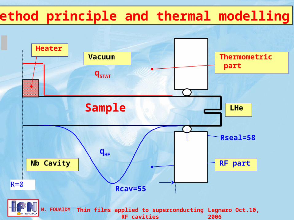
R=0Rcav=55
Rseal=58
qHF
Nb Cavity RF part
LHe
Thermometric part
qSTAT
Vacuum Heater
Method principle and thermal modelling
Sample
M. FOUAIDY Thin films applied to superconducting RF cavities Legnaro Oct.10, 2006
Simulation parameters:-Tbath=1.715 K
-experimental copper thermal conductivity
-kapitza conductance at sample -LHe interface:hK=4000W/m2.K
0
20
40
60
80
100
120
140
0 5 10 15 20 25 30 35 40 45 50 55
r (mm)
T
(mK
)
Pstat
Prf
P R H H S dS
HH
J krJ kr
P H aR bR H cR H
RF s s sS
SSMAX
RF SMAX SMAX SMAX
1
22
11
20 1 2
2
( ) * ( )
( )( )
( )
max
kp
rcav 11
No RF dissipation at the indium seal 2nd order polynomial law parametrization of Rs=f(Hs) Total dissipated RF power PRF depending on the surface magnetic field Hs
p11:J1‘s first zero
For radius r>40mm
PSTAT=PRF TSTAT= T RF
Determination of RS coefficients
(a, b, c) by least square method

M. FOUAIDY Thin films applied to superconducting RF cavities Legnaro Oct.10, 2006
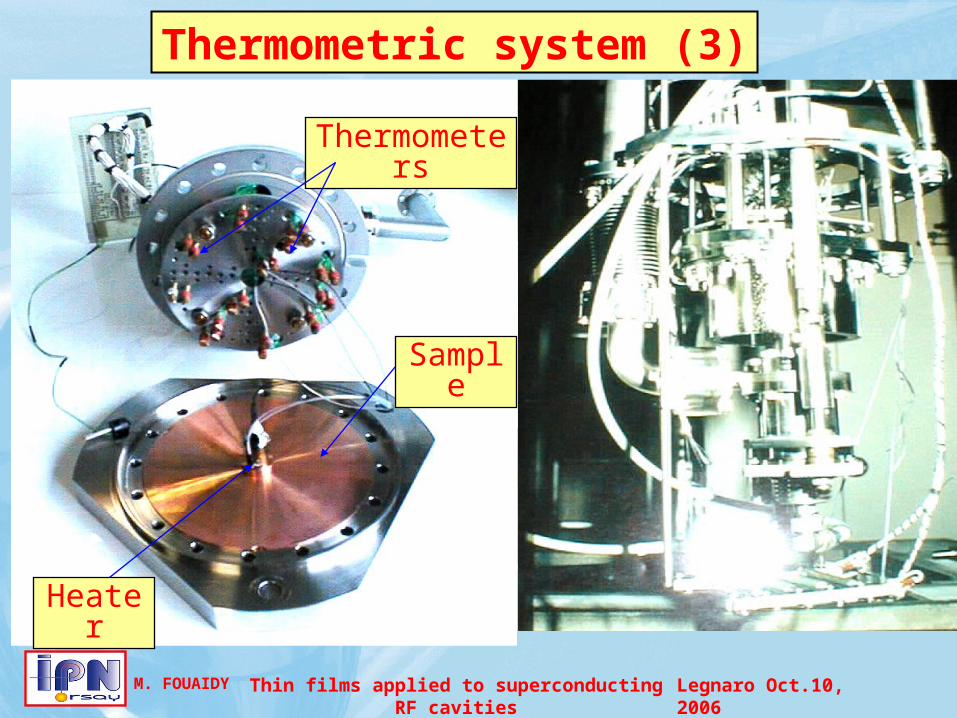
Dismountable assembly of 24 Surface thermometers in a vacuum chamber
Four subsets at 90° apart at 6 radial positions from 12.4mm up to 47.4mm (Step r=7mm) Calibration heater (12 OFHC rod) located at the centre of the test-sample Calibrated thermometer (1.5K-60K) placed near the heater/sample boundary control of the heater temperature and determination of the heat leaks Two reference thermometers (Calibrated Germanium and Carbon resistor)
Accurate measurements of Tbath during thermometers
calibration (R vs T curve) and during
measurements sequences (T vs qSTAT and T vs qHF)
Thermometric system (1)

M. FOUAIDY Thin films applied to superconducting RF cavities Legnaro Oct.10, 2006
Bulk Niobium cavity : TE011 mode f=4GHz TE012 mode f=5.6GHz Calibration heater 24 thermometersVacuum chamber Heater thermometer (Heat leaks)
Thermometric system (2)
M. FOUAIDY Thin films applied to superconducting RF cavities Legnaro Oct.10, 2006
Sample
Thermometers
Heater
Thermometric system (3)

M. FOUAIDY Thin films applied to superconducting RF cavities Legnaro Oct.10, 2006
Measured and simulated temperature profiles
QSTAT
(mW)
Type T12
(mK)
T11
(mK)
T10
(mK)
T 9
(mK)
T 8
(mK)
220 Computed 36.5 29.4 24.4 20.7 17.6
220 Measured 36.8 29.2 25.3 20.9 17.5
1990 Computed 320 260.3 218.7 186.6 160.5
1990 Measured 323 254.6 228.4 187.8 159.2
Hs(A/mm)
Type T12(mK)
T11(mK)
T10(mK)
T 9(mK)
T 8(mK)
14 Computed 25.3 24.8 23.6 21.7 19.2
14 Measured 21.1 20.4 20.1 18.7 18.5
33 Computed 209 205.4 195.9 179.6 159
33 Measured 200.1 194.1 188.3 173.1 162.9

M. FOUAIDY Thin films applied to superconducting RF cavities Legnaro Oct.10, 2006
Minimum detectable heating : ~0.1mK at T=1.7K and T=4.2K
Accuracy: calorimetric versus RF method at f=4 GHz
Sensitivity and accuracy of the method
T=1.7K T=4.2K
T=1.7K T=4.2K
The accuracy of calorimetric method is ~5 times better than RF method

M. FOUAIDY Thin films applied to superconducting RF cavities Legnaro Oct.10, 2006
Validation of the calorimetric method by comparison with RF measurement (1)
0
50
100
150
200
250
300
350
400
450
0 50 100 150 200Hs(Oe)
RsTh RsHF
5000
6000
7000
8000
9000
10000
11000
12000
13000
0 20 40 60 80 100 120Hs (Oe)
Rs(n
)
RsTh
RsHF
f=5.6 GHz
f=4 GHz
f=4 GHz
f=5.6 GHz
T=1.7KT=4.2K
Tests of a Bulk niobium sample (Solid dots: usual RF method, Solid line : calorimetric method)
Good agreement between the two methodsFor bulk niobium the field is limited by RF heating (Disk cooled by liquid helium at the lateral rim only)
Bs(Oe) Bs(Oe)
RS(n) RS(n)

M. FOUAIDY Thin films applied to superconducting RF cavities Legnaro Oct.10, 2006
0
50
100
150
200
0 10 20 30 40Bs (mT)
Rs(
n)
HFHF refroidissement latéralTH refroidissement latéral
5000
6000
7000
8000
9000
0 5 10 15Bs (mT)R
s(n
)
Validation of the calorimetric method by comparison with RF measurement (2)Tests of a Bulk niobium sample (dots: usual RF method, Solid line : calorimetric method)
T=1.7KT=4.2K
f=4 GHzf=4 GHz
Rim cooling
Disk cooling
For bulk niobium, the cooling conditions have a strong effect on the maximum RF field achieved and on surface resistance at high field (Joule heating)

M. FOUAIDY Thin films applied to superconducting RF cavities Legnaro Oct.10, 2006
Test of a niobium film sputtered onto a copper substrate at T=1.7K
0200
400600
8001000
12001400
1600
0 10 20 30 40Bs (mT)
Rs(
n)
HFHF refroidissement latéralTh refroidissement latéral
T=1.7K
f=5.6 GHz
Good agreement between the two methods: for six tests performed at 1.7 K the difference is 15%-20%For sputtered niobium films the field is not limited by RF heating Efficient conduction cooling by copper substrate (Disk cooled by liquid helium at the lateral rim only)
M. FOUAIDY Thin films applied to superconducting RF cavities Legnaro Oct.10, 2006
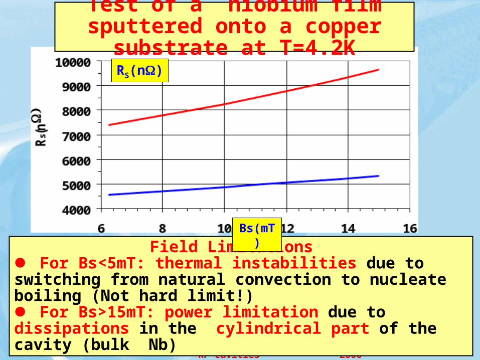
Field Limitations For Bs<5mT: thermal instabilities due to switching from natural convection to nucleate boiling (Not hard limit!) For Bs>15mT: power limitation due to dissipations in the cylindrical part of the cavity (bulk Nb)
Test of a niobium film sputtered onto a copper substrate at T=4.2K
RS(n)
Bs(mT)
M. FOUAIDY Thin films applied to superconducting RF cavities Legnaro Oct.10, 2006
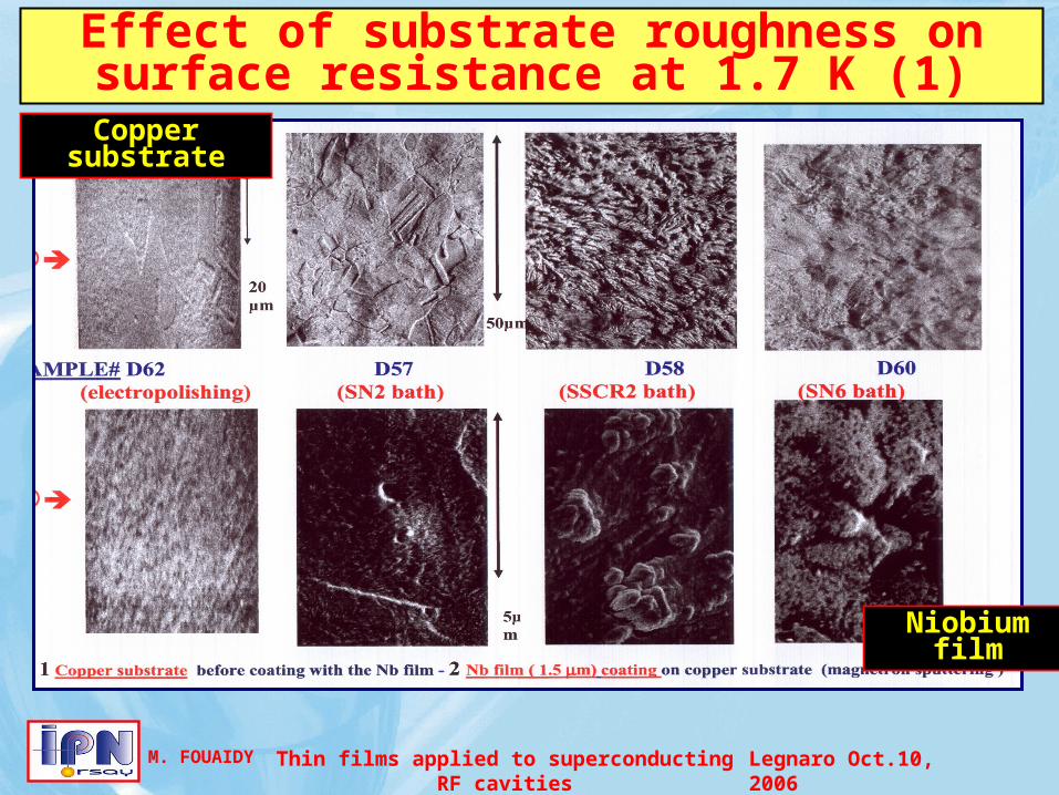
Effect of substrate roughness on surface resistance at 1.7 K (1)
Copper substrate
Niobium film

M. FOUAIDY Thin films applied to superconducting RF cavities Legnaro Oct.10, 2006
<Rs>(B) par méthode thermométriqueMode Te011 Tb=1,7K
0
500
1000
1500
2000
2500
3000
0 5 10 15 20 25 30 35 40B(mT)
Rs(
n
)
d57
d58
d60
d62
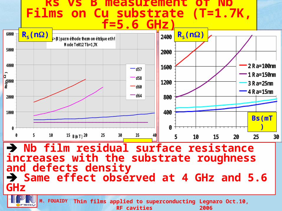
Rs vs B measurement of Nb Films on Cu substrate (T=1.7K, f=4GHz)
Nb film residual surface resistance increases with the substrate roughness and defects density Use clean and smooth substrate with intermediate layer for of lattice matching and improve superconducting properties
Bs(mT) Bs(mT)
RS(n)
RS(n)
M. FOUAIDY Thin films applied to superconducting RF cavities Legnaro Oct.10, 2006
Rs vs B measurement of Nb Films on Cu substrate (T=1.7K, f=5.6 GHz)
<Rs>(B) par méthode thermométrique et hf Mode Te012 Tb=1,7K
0
1000
2000
3000
4000
5000
6000
0 5 10 15 20 25 30 35 40B(mT)
Rs(n
)
d57
d58
d60
d64
RS(n)
Bs(mT)
Bs(mT)
RS(n)
Nb film residual surface resistance increases with the substrate roughness and defects density Same effect observed at 4 GHz and 5.6 GHz