Embed Size (px)
Citation preview

Copyright © 2008 Linear Technology. All rights reserved.
Getting Started

Copyright © 2008 Linear Technology. All rights reserved.
Draft a Design Using the Schematic Editor

© 2008 Linear Technology
14
New Schematic
Start with a New Schematic
Left click on the New Schematic symbol in the Schematic Editor Toolbar
LTspice is also a great schematic capture

© 2008 Linear Technology
15
Add a Linear Technology MacromodelAdd Component
Left click on the Component symbol in the Schematic Editor ToolbarEnter “root” part to search for the model (e.g. 3411)Left click on OK

© 2008 Linear Technology
16
Getting the Latest DatasheetUse the macromodel’s shortcuts to download the Datasheetas a reference for your design
Hold Ctrl key and right click (Ctrl – right click) over the LT macromodel’s symbolLeft click on Go to Linear website for datasheet on the dialog box that appears
You can also open the macromodel's test fixture as a draft starting point

© 2008 Linear Technology
17
Adding Circuit Elements
To cancel or quit a component type, click the right mouse button
RotateMirror
Place DiodePlace Inductor
Place CapacitorPlace Resistor
Left click on the desired component in the Schematic Editor ToolbarLeft click on Rotate or Mirror to adjust orientation
Alternate you can also use Ctrl – R and Ctrl – M key shortcutsMove the mouse to the position you want to place itLeft click to place it

© 2008 Linear Technology
18
Adding Sources, Loads & Additional Circuit Elements
Additional Circuit Elements Like Sources and Loads
Left click on the Component symbol in the Schematic Editor ToolbarSearch directory structure for desired circuit element (e.g. load and voltage)Left click on OKMove the mouse to the position you want to place itLeft click to place it

© 2008 Linear Technology
19
Highlights of Additional Circuit ElementsLeft click on the Component symbol in the Schematic Editor Toolbar for a directory of additional circuit elements:
Arbitrary behavioral sourceVoltage dependent voltageCurrent dependent currentVoltage dependent currentCurrent dependent voltageIndependent current sourceJFET transistorMutual inductanceMOSFET transistor
Lossy transmission lineBipolar transistorVoltage controlled switchLossless transmission lineUniform RC-lineIndependent voltage sourceCurrent controlled switchSubcircuitMESFET transistor…many more

© 2008 Linear Technology
20
Drawing Lines and Labeling Nodes
LinesLeft click on the Draw Wire in the Schematic Editor ToolbarLeft click a blue box (terminal)Define the line’s path with a left click over intermediate pointsLeft click on another blue box (terminal)
Draw WirePlace GroundLabel Node
Do not forget to place a ground in your design, it is
required for simulation!

© 2008 Linear Technology
21
Editing Circuit Elements
To organize your layout, use the Drag option to move circuit elements around and to adjust lines between terminals
MoveDragUndo
Redo
DeleteDuplicate
Left click on the desired editing optionLeft click on the circuit element

© 2008 Linear Technology
22
Editing Circuit Elements AttributesRight click on the component symbol to modify attributes
Right click on the text next to the component to edit the visible attribute and label
Pointer will turn into a text caret

© 2008 Linear Technology
23
Use Labels to Specify Units in Circuit Elements Attributes
K = k = kilo = 103
MEG = meg = 106
G = g = giga = 109
T = t = terra = 1012
M = m = milli = 10-3U = u = micro = 10-6N = n = nano = 10-9P = p = pico = 10-12F = f = femto = 10-15
HintsUse MEG to specify 106, not MEnter 1 for 1 Farad, not 1F

© 2008 Linear Technology
24
Circuit Elements DatabaseSome components have an available database of manufacturers’ attributes
Resistors, capacitors, inductors, diodes, Bipolar transistors, MOSFET transistors, JFET transistorsIndependent voltage and current sources
To configure a component to a manufacture’s attributes
Right click on the component symbolLeft click on Select… or Pick New…Left click on a selected deviceLeft click on OK

© 2008 Linear Technology
25
Editing Voltage Sources and LoadsVoltage Source
Right click the voltage symbolEnter DC voltage value and (optional) Series Resistance Left click on OK
Load (current)Right click on the load symbolEnter DC current valueLeft click on OK

© 2008 Linear Technology
26
Summary of Schematic Editor ToolbarPlace Circuit Element
Place DiodePlace Inductor
Place CapacitorPlace Resistor
Label NodePlace Ground
Draw Wire
MoveDragUndo
RedoRotate
MirrorPlace Comment
Place SPICE directive
DeleteDuplicate
Paste b/t SchematicsFind

Copyright © 2008 Linear Technology. All rights reserved.
Run and Probe a Circuit

© 2008 Linear Technology
28
Simulation CommandsTo run a simulation, specify the type of analysis to be performedThere are six different types of analyses:
Transient analysisSmall signal ACDC sweepNoiseDC transfer functionDC operating point
Simulation commands are placed on the schematic as textCalled dot commands
More information on simulation and dot commands are available in
SwitcherCAD III/LTspice User Guide

© 2008 Linear Technology
29
Editing Simulation CommandsLeft click on Simulation menu
Left click on Edit Simulation CmdAs a starting point in a simulation
Left click on Transient tab
Enter a Stop TimeYou may need to adjust this again later
Select OK
Demo Circuits and Test Fixtureshave predefined Simulations
Commands

© 2008 Linear Technology
30
Running a CircuitRun
If model is not found please Sync Release under Help menu to update LTspice
© 2008 Linear Technology
31
Current probe cursor
Probing a Circuit & Waveform Viewer Left click on any wire to plot the voltage on the waveform viewer
Left click on the body of the component to plot the current on the waveform viewer
Convention of positive current is in the direction into the pin
Voltage probe cursor

© 2008 Linear Technology
32
Probing a Demo Circuit and Test FixtureDemo Circuits and Test Fixtures have INs and OUTs clearly labeled to help you quickly select themTo view the waveform left click on IN and OUT
Left Click Here for Output
Waveform
Left Click Here for
Input Waveform
© 2008 Linear Technology
33
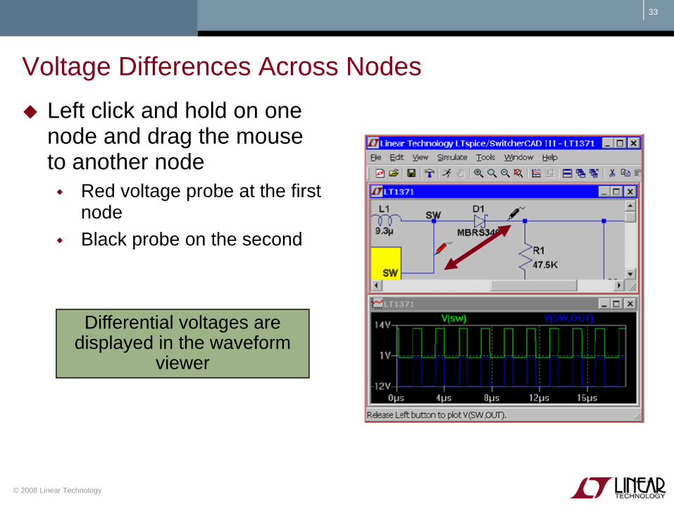
Voltage Differences Across NodesLeft click and hold on one node and drag the mouse to another node
Red voltage probe at the first nodeBlack probe on the second
Differential voltages are displayed in the waveform
viewer

© 2008 Linear Technology
34
Plot PlanesMultiple plot panes can be displayed on one window to allow better separation between traces permitting different traces to be independently autoscaled
Right click in the waveform paneSelect Add Plot PaneLeft click and hold to drag a label to a new plot pane

© 2008 Linear Technology
35
Zooming In and Out in the Waveform ViewerTo zoom in
Left click and hold as you drag a box about the region you wish to zoom in then release
To zoom outRight click and select Zoom to Fit or Zoom Back
Zoom InPan
Zoom OutAutoscale

© 2008 Linear Technology
36
Measuring VRipple, IRipple and Time (Frequency)Drag a box about the region you wish to measure (peak to peak over a period)
Left click and hold to drag a box over the portion of interestView the lower left hand side of the screen
To avoid resizing, shrink your box before you let go of the left mouse click or use the Undo command in the Edit menu
To view SMPS voltage ripple you will need to zoom into a narrow section
since waveform is initially compressed to full range

© 2008 Linear Technology
37
Average/RMS Current or Voltage Calculations Hold down Ctrl and left click on the I or V trace label in the waveform viewer

© 2008 Linear Technology
38
Instantaneous & Average Power DissipationInstantaneous Power Dissipation
Hold down the ALT key and left click on the symbol of the componentPointer will change to a thermometer Plotted in units of Watts
Average Power Dissipation Hold down the Ctrl key and left click on the trace labelpower dissipation waveform

© 2008 Linear Technology
53
Independent LTspice Users’ GroupThe group has a section of files and messages with additional tutorials, libraries, and examples
http://groups.yahoo.com/group/LTspice/Join LTspice Users’ Group
Email [email protected]=Subscribe