Embed Size (px)
Citation preview
LTC4110
14110fb
Battery BackupSystem Manager
FEATURES
APPLICATIONS
DESCRIPTIONThe LTC®4110 is a complete single chip, high effi ciency, fl yback battery charge and discharge manager with auto-matic switchover between the input supply and the backup battery or super capacitor. The IC provides four modes of operation: battery backup, battery charge, battery calibra-tion and shutdown. Battery backup and battery charge are automatic standalone modes, while the optional calibration mode requires a CPU host to communicate over an SMBus. During calibration the fl yback charger is used in reverse to discharge the battery with a programmable constant current into the system load eliminating heat generation. Three status outputs can be individually reconfi gured over the SMBus to become GPIOs. User programmable over-discharge protection is provided. The SHDN pin isolates the battery to support shipping the product with a charged battery installed.
Multiple LTC4110s can be combined to form a redundant battery backup system or increase the number of battery packs to achieve longer backup run times.
The LTC4110 is available in a low profi le (0.75mm), 38-pin 5mm × 7mm QFN package. The QFN features an exposed metal die mount pad for optimum thermal performance.
n Complete Backup Battery Manager for Li-Ion/Polymer, Lead Acid, NiMH/NiCd Batteries and Super Capacitors
n Charge and Discharge Battery with Voltages Above and Below the Input Supply Voltage
n “No Heat” Battery Calibration Discharge Using System Load
n Automatic Battery Backup with Input Supply Removal Using PowerPath™ Control
n Standalone for Li-Ion/Polymer, SLA, and Supercapsn Optional SMBus/I2C Support Allows Battery
Capacity Calibration Operation with Hostn Over- and Under-Battery Voltage Protectionn Adjustable Battery Float Voltagen Precision Charge Voltage ±0.5%n Programmable Charge/Calibration Current Up to
3A with ±3% Accuracyn Optional Temperature Qualifi ed Chargingn Wide Backup Battery Supply Range: 2.7V to 19Vn Wide Input Supply Range: 4.5V to 19Vn 38-Lead (5mm × 7mm) QFN Package
n Backup Battery Systemsn Server Memory Backupn Medical Equipmentn High Reliability Systems
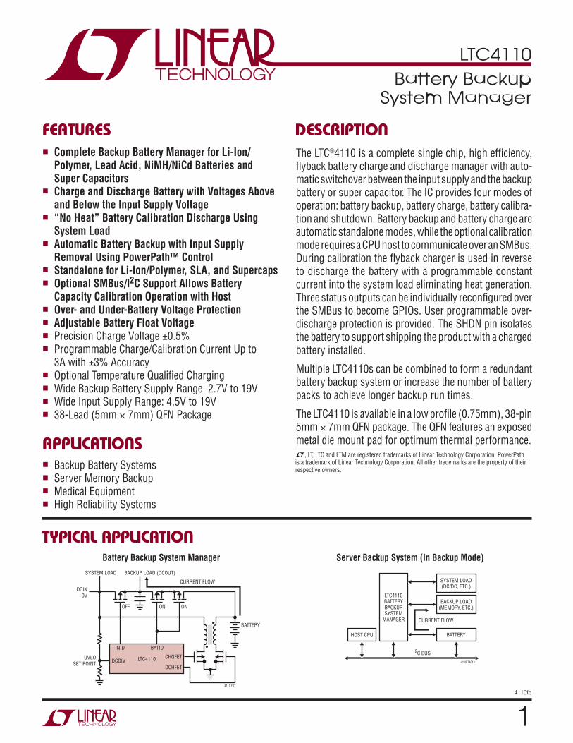
Battery Backup System Manager Server Backup System (In Backup Mode)
TYPICAL APPLICATION
L, LT, LTC and LTM are registered trademarks of Linear Technology Corporation. PowerPath is a trademark of Linear Technology Corporation. All other trademarks are the property of their respective owners.
LTC4110
INID BATID
DCDIV
DCHFET
CHGFETUVLO
SET POINT
BACKUP LOAD (DCOUT)
CURRENT FLOW
SYSTEM LOAD
BATTERY
DCIN0V
ON ONOFF
4110 F01
4110 TA01b
LTC4110BATTERYBACKUPSYSTEM
MANAGER
HOST CPU BATTERY
SYSTEM LOAD(DC/DC, ETC.)
I2C BUS
BACKUP LOAD(MEMORY, ETC.)
CURRENT FLOW
LTC4110
24110fb
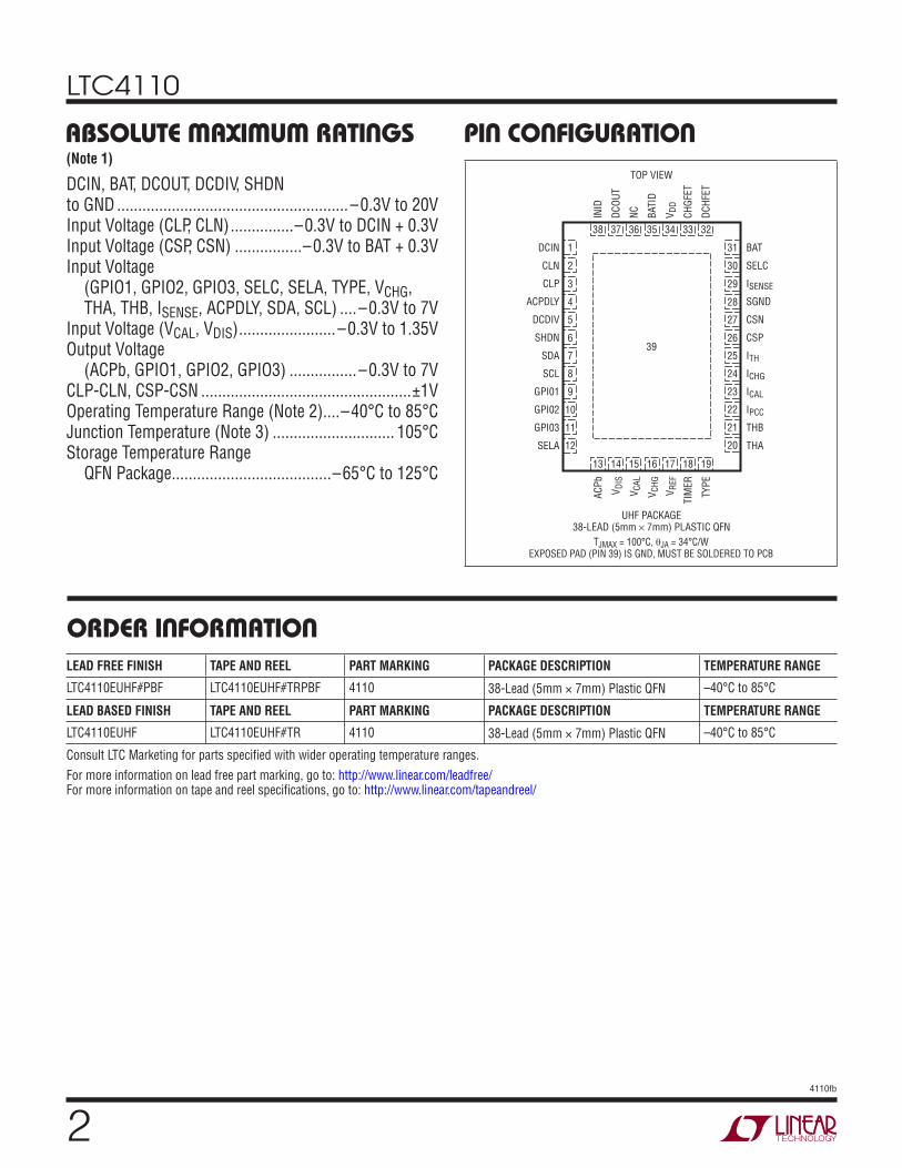
PIN CONFIGURATIONABSOLUTE MAXIMUM RATINGS
DCIN, BAT, DCOUT, DCDIV, SHDN to GND ....................................................... –0.3V to 20VInput Voltage (CLP, CLN) ...............–0.3V to DCIN + 0.3VInput Voltage (CSP, CSN) ................–0.3V to BAT + 0.3VInput Voltage
(GPIO1, GPIO2, GPIO3, SELC, SELA, TYPE, VCHG, THA, THB, ISENSE, ACPDLY, SDA, SCL) .... –0.3V to 7V
Input Voltage (VCAL, VDIS) ....................... –0.3V to 1.35VOutput Voltage
(ACPb, GPIO1, GPIO2, GPIO3) ................ –0.3V to 7VCLP-CLN, CSP-CSN ..................................................±1VOperating Temperature Range (Note 2)....–40°C to 85°CJunction Temperature (Note 3) ............................. 105°CStorage Temperature Range
QFN Package ......................................–65°C to 125°C
(Note 1)
13 14 15 16
TOP VIEW
39
UHF PACKAGE38-LEAD (5mm 7mm) PLASTIC QFN
17 18 19
38 37 36 35 34 33 32
24
25
26
27
28
29
30
31
8
7
6
5
4
3
2
1DCIN
CLN
CLP
ACPDLY
DCDIV
SHDN
SDA
SCL
GPI01
GPI02
GPI03
SELA
BAT
SELC
ISENSE
SGND
CSN
CSP
ITH
ICHG
ICAL
IPCC
THB
THA
INID
DC
OU
T
NC
BA
TID
VD
D
CH
GFE
T
DC
HFE
T
AC
Pb
VD
IS
VC
AL
VC
HG
VR
EF
TIM
ER
TYP
E
23
22
21
20
9
10
11
12
TJMAX = 100°C, θJA = 34°C/WEXPOSED PAD (PIN 39) IS GND, MUST BE SOLDERED TO PCB
ORDER INFORMATIONLEAD FREE FINISH TAPE AND REEL PART MARKING PACKAGE DESCRIPTION TEMPERATURE RANGE
LTC4110EUHF#PBF LTC4110EUHF#TRPBF 4110 38-Lead (5mm × 7mm) Plastic QFN –40°C to 85°C
LEAD BASED FINISH TAPE AND REEL PART MARKING PACKAGE DESCRIPTION TEMPERATURE RANGE
LTC4110EUHF LTC4110EUHF#TR 4110 38-Lead (5mm × 7mm) Plastic QFN –40°C to 85°C
Consult LTC Marketing for parts specifi ed with wider operating temperature ranges.
For more information on lead free part marking, go to: http://www.linear.com/leadfree/ For more information on tape and reel specifi cations, go to: http://www.linear.com/tapeandreel/
LTC4110
34110fb
ELECTRICAL CHARACTERISTICS The l denotes the specifi cations which apply over the full operating temperature range, otherwise specifi cations are at TA = 25°C. Unless otherwise specifi ed, VDCIN = VDCOUT = VDCDIV = 12V, VBAT = 8.4V, GND = SGND = CLP = CLN = SHDN = 0V and RVREF = 49.9k. All currents into device pins are positive and all currents out of device pins are negative. All voltages are referenced to GND, unless otherwise specifi ed.
SYMBOL PARAMETER CONDITIONS MIN TYP MAX UNITS
Power Input
DCIN Operating Voltage Range Charge or Calibration Modes l 4.5 19 V
DCOUT Operating Voltage Range Charge or Calibration Modes l 4.5 19 V
Backup Mode l 2.7 19 V
VBAT Operating Voltage Range Backup Mode l 2.7 19 V
ISPLY Supply Current (IDCIN + IDCOUT) in Idle Mode (Note 4)
2 3 mA
IBIDL Battery Current in Idle Mode (Notes 4 and 5) 30 45 μA
IBBU Battery Current in Backup Mode (Note 5) VDCIN = 0 2 3 mA
IBSD Battery Current in Shutdown (Note 5) VSHDN = VBAT, VDCIN = 0 20 45 μA
VUVI Undervoltage Lockout Exit Threshold VDCIN Increasing l 3.7 4 4.45 V
VUVD Undervoltage Lockout Entry Threshold VDCIN Decreasing l 3.4 3.7 4.1 V
VUVH Undervoltage Lockout Hysteresis 400 mV
VDD Regulator
VDD Output Voltage No Load l 4.5 4.75 5 V
VDD(MIN) Output Voltage IDD = –10mA l 4.25 V
Charging Performance
VFTOL Charge Float Voltage Accuracy 4.20V for Li-Ion. 2.35V for Lead Acid (Note 8)VCHG = GND –5°C < TA < 85°C (Note10)–40°C < TA < 85°C l
–0.5
–0.8–1
0.5
0.81
%
%%
VFATOL Charge Float Voltage Adjust Accuracy 0.3V and –0.3V for Li-Ion Batteries,0.15V and –0.15V for Lead Acid Batteries (Note 8)
l –2 2 %
IBTOL Bulk Charge Current Accuracy (Note 7) VCSP – VCSN =100mVVBAT ≥ 3.1V–40°C < TA < 85°C l
–3
–5
3
5
%
%
IPTOL Preconditioning and Wake-Up Current Accuracy (Note 7)
VBAT ≥ 3.3V (Note 8), VCSP – VCSN = 10mV; Li-Ion and NiMH/NiCd Batteries Only
–30 30 %
VBAT ≤ 3.3 (Note 8), VCSP – VCSN = 10mV; Li-Ion and NiMH/NiCd Batteries Only
–40 40 %
ISKVA Voltage Error Amplifi er Sink Current at ITH Pin VITH = 2V 96 μA
ISRCA Current Error Amplifi er Source Current at ITH Pin
VITH = 2V –24 μA
ISKCA Current Error Amplifi er Sink Current at ITH Pin VITH = 2V 24 μA
IVCHG VCHG Pin Bias Current VCHG = 1.25V –100 100 nA
VBC Bulk Charge Threshold Voltage;VBAT Increasing (Note 8)
Li-Ion, VCHG = GNDNiMH/NiCd
2.800.84
3.000.90
3.200.96
VV
VBCH Bulk Charge Threshold Voltage Hysteresis; VBAT Decreasing (Note 8)
Li-Ion, VCHG = GNDNiMH/NiCd
8540
mVmV
VAR Auto Recharge Threshold Voltage;VBAT Decreasing
Standard Li-Ion Only;Specifi ed as Percentage of Float Voltage 93 95 97 %
VARH Auto Recharge Threshold Hysteresis Voltage; VBAT Increasing
Standard Li-Ion Only; Specifi ed as Percentage of Float Voltage
2 %
LTC4110
44110fb
ELECTRICAL CHARACTERISTICS The l denotes the specifi cations which apply over the full operating temperature range, otherwise specifi cations are at TA = 25°C. Unless otherwise specifi ed, VDCIN = VDCOUT = VDCDIV = 12V, VBAT = 8.4V, GND = SGND = CLP = CLN = SHDN = 0V and RVREF = 49.9k. All currents into device pins are positive and all currents out of device pins are negative. All voltages are referenced to GND, unless otherwise specifi ed.
SYMBOL PARAMETER CONDITIONS MIN TYP MAX UNITS
VBOV Battery Overvoltage Threshold;VBAT Increasing
All Li-Ion, Lead Acid as Percentage of Float VoltageNiMH/NiCd (Note 8)
1051.80
107.51.85
1101.90
%V
VBOVH Battery Overvoltage Threshold Hysteresis; VBAT Increasing.
All Li-Ion, Lead Acid as Percentage of Float VoltageNiMH/NiCd (Note 8)
240
%mV
VREF Reference Pin Voltage Range l 1.208 1.220 1.232 V
FTMR Programmed Timer Accuracy CTIMER = 47nF l –15 0 15 %
tTIMEOUT Time Between Receiving Valid ChargingCurrent() and ChargingVoltage() Commands. Wake-Up Timer.
l 140 175 210 sec
Calibration Performance
VCTOL Calibration Cut-Off Default Voltage Accuracy; VBAT Decreasing
2.75V for Li-Ion, 1.93V for Lead Acid,VCAL = GND (Note 8), 0.95V for NiMH/NiCd l
–1.1–1.3
1.11.3
%%
VCTOLH Calibration Cut-Off Default Voltage Hysteresis; VBAT Increasing. (Note 8)
Li-IonLead AcidNiMH/NiCd
855040
mVmVmV
VCATOL Calibration Cut-Off Voltage Adjust Accuracy ±400mV for Li-Ion, ±300mV for Lead Acid,±200mV for NiMH/NiCd (Note 8)
l –1.5 1.5 %
IFTOL Calibration Current Accuracy (Note 7) VCSP – VCSN = –100mV l –5 5 %
IVCAL VCAL Pin Leakage Current VCAL = 1.25V –100 100 nA
IBDT Back-Drive Current Limit Threshold VCLP – VCLN DecreasingVCLN = VDCIN
l 7 10 13 mV
IBDH Back-Drive Current Limit Threshold Hysteresis VCLP – VCLN IncreasingVCLN = VDCIN
1 mV
VOVP Calibration Mode Input Overvoltage Comparator DCDIV Pin Threshold
VDCDIV Rising l 1.4 1.5 1.6 V
VOVPH Calibration Mode Input Overvoltage Comparator DCDIV Pin Hysteresis
VDCDIV Falling 100 mV
AC Present and Discharge Cut-Off Comparators
VAC AC Present Comparator DCDIV Pin Threshold VDCDIV Falling l 1.196 1.22 1.244 V
VACH AC Present Comparator DCDIV Pin Hysteresis VDCDIV Rising 50 mV
IAC AC Present Comparator DCDIV Pin Input Bias Current
VDCDIV = 1.25V 100 nA
tAC ACPb Pin Externally Programmed Falling Delay CACPDLY = 100nF, RVREF = 49.9k,VDCDIV Stepped From 1.17V to 1.30V 8 10 12 ms
VDTOL Discharge Cut-Off Default Voltage Accuracy; VBAT Decreasing
2.75V for Li-Ion, 1.93V for Lead Acid,VDIS = GND, 0.95V for NiMH/NiCd
l –1.5 1.5 %
VDTOLH Discharge Cut-Off Default Voltage Hysteresis; VBAT Increasing (Note 8)
Li-IonLead acidNiMH/NiCd
855040
mVmVmV
VDATOL Discharge Cut-Off Voltage Adjust Accuracy ±400mV for Li-Ion, ±300mV for Lead Acid,±200mV for NiMH/NiCd
l 2 2 %
IVDIS VDIS Pin Bias Current VDIS = 1.25V –100 100 nA
LTC4110
54110fb
ELECTRICAL CHARACTERISTICS The l denotes the specifi cations which apply over the full operating temperature range, otherwise specifi cations are at TA = 25°C. Unless otherwise specifi ed, VDCIN = VDCOUT = VDCDIV = 12V, VBAT = 8.4V, GND = SGND = CLP = CLN = SHDN = 0V and RVREF = 49.9k. All currents into device pins are positive and all currents out of device pins are negative. All voltages are referenced to GND, unless otherwise specifi ed.
SYMBOL PARAMETER CONDITIONS MIN TYP MAX UNITS
Input and Battery Ideal Diodes and Switches
VFR Forward Regulation Voltage (VDCIN-VDCOUT, VBAT -VDCOUT)
2.7V ≤ VDCIN ≤ 19V l 10 20 32 mV
VREV Reverse Voltage Turn-Off Voltage (VDCIN-VDCOUT, VBAT -VDCOUT)
2.7V ≤ VDCIN ≤ 19V l –30 –18 –8 mV
VGON “ON” Gate Clamping Voltage (VDCIN-VINID, VBAT -VBATID)
IINID, IBATID = 1μA 7 8.3 9.7 V
VGOFF “OFF” Gate Voltage (VDCIN-VINID, VBAT-VBATID) IINID, IBATID = –10μAVSHDN = 0V and VDCIN (Shutdown)
0.25 V
VFO BATID Fast-On Voltage Comparator Threshold IBATID > 500μA 45 100 mV
tIIDONtIIDOFF
INID Pin Delay Times
Turn “ON” Turn “OFF”
CINID = 10nFDCIN is Switched Between 12.2V and 11.8VFrom DCOUT – VGOFF to DCOUT –6VFrom DCOUT – VGON to DCOUT –1.5V
4508
70020
μsμs
tBIDONtBIDOFF
BATID Pin Delay Times
Turn “ON” Turn “OFF”
CBATID = 2.5nF BAT is Switched Between 12.2V and 11.8VFrom DCOUT – VGOFF to DCOUT –6VFrom DCOUT – VGON to DCOUT –1.5V
158
6020
μsμs
PWM Flyback Converter
VOHF CHGFET, DCHFET High ICHGFET, IDCHFET = –1mA 4.5 4.75 5.25 V
VOLF CHGFET, DCHFET Low ICHGFET, IDCHFET = 1mA 50 mV
VOLFX CHGFET, DCHFET in Shutdown and Backup Modes
VDCIN = VDCDIV = VDCOUT = 0V (Shutdown Mode), VDCIN = VDCDIV = 0V (Backup Mode)ICHGFET, IDCHFET = 1μA
100 mV
tRtF
CHGFET, DCHFET Transition TimesRise TimeFall Time
CLOAD = 1.6nF, 20% to 80%CLOAD = 1.6nF, 20% to 80%
3515
6565
nsns
FPWM PWM Oscillator Switching Frequency l 255 300 340 kHz
SafetySignal Decoder and Thermistor Interface
SSOR SafetySignal DecoderSafetySignal Trip (RES_COLD/RES_OR)
RTHA = 1130Ω ±1%, CTH = 1nF (Note 6) RTHB = 54.9k ±1%. Smart Batteries and Li-Ion Only
l 95 100 105 k
SSCLD SafetySignal DecoderSafetySignal Trip (RES_IDEAL/RES_COLD)
RTHA = 1130Ω ±1%, CTH = 1nF (Note 6) RTHB = 54.9k ±1% Smart Batteries and Li-Ion Only
l 28.5 30 31.5 k
SSIDL SafetySignal DecoderSafetySignal Trip (RES_HOT/RES_IDEAL)
RTHA = 1130Ω ±1%, CTH = 1nF (Note 6) RTHB = 54.9k ±1%Smart Batteries and Li-Ion Only
l 2.85 3 3.15 k
SSHOT SafetySignal DecoderSafetySignal Trip (RES_UR/RES_HOT)
RTHA = 1130Ω ±1%, CTH = 1nF (Note 6) RTHB = 54.9k ±1%Smart Batteries and Li-Ion Only
l 425 500 575 Ω
VHOT THB Pin Hot Threshold Voltage VTHB Decreasing; Lead Acid Only l 0.28 •VTHA
0.30 •VTHA
0.36 •VTHA
V
VHOTH THB Pin Hot Threshold Hysteresis Voltage VTHB Increasing; Lead Acid Only 50 mV
VREM THB Pin Battery Removal Threshold Voltage VTHB Increasing; Lead Acid Only l 0.90 •VTHA
0.94 •VTHA
0.96 •VTHA
V
LTC4110
64110fb
Note 1: Stresses beyond those listed under Absolute Maximum Ratings
may cause permanent damage to the device. Exposure to any Absolute
Maximum Rating condition for extended periods may affect device
reliability and lifetime. Specifi c functionality or parametric performance
of the device beyond the limits expressly given in the Electrical
Characteristics table is not implied by these maximum ratings.
Note 2: The LTC4110E is guaranteed to meet performance specifi cations
from 0°C to 85°C. Specifi cations over the –40°C to 85°C operating
temperature range are assured by design, characterization and correlation
with statistical process controls.
Note 3: This IC includes overtemperature protection that is intended
to protect the device during momentary overload conditions.
Overtemperature protection will become active at a junction temperature
greater than the maximum operating junction temperature. Continuous
operation above the specifi ed maximum operation temperature may result
in device degradation or failure. Operating junction temperature TJ (in
°C) is calculated from the ambient temperature TA and the average power
dissipation PD (in watts) by the formula TJ = TA + θJA • PD.
ELECTRICAL CHARACTERISTICS The l denotes the specifi cations which apply over the full operating temperature range, otherwise specifi cations are at TA = 25°C. Unless otherwise specifi ed, VDCIN = VDCOUT = VDCDIV = 12V, VBAT = 8.4V, GND = SGND = CLP = CLN = SHDN = 0V and RVREF = 49.9k. All currents into device pins are positive and all currents out of device pins are negative. All voltages are referenced to GND, unless otherwise specifi ed.
Note 4: The LTC4110 is idle with no application load. It is not charging
or calibrating the battery and is not in backup or shutdown mode. The
internal clock is running and the SMBus is functional.
Note 5: Combined current of CSP, CSN and BAT pins set to VBAT with no
application load.
Note 6: CTH is defi ned as the sum of capacitance on THA, THB
SafetySignal.
Note 7: Does not include tolerance of current sense or current
programming resistors.
Note 8: Given as a per cell voltage referred to the BAT pin (VBAT/number of
series cells).
Note 9: Refer to System Management Bus Specifi cation, Revision 1.1,
section 2.1 for Timing Diagrams and section 8.1, for tLOW and tTIMEOUT
requirements.
Note 10: Specifi cations over the –5°C to 85°C operating ambient
temperature range are assured by design, characterization and correlation
with statistical process controls.
SYMBOL PARAMETER CONDITIONS MIN TYP MAX UNITS
VREMH THB Pin Battery Removal Threshold Hysteresis Voltage
VTHB Decreasing; Lead Acid Only 25 mV
Logic and Status Output Levels
VILS SCL/SDA Input Pins Low Voltage l 0.8 V
VIHS SCL/SDA Input Pins High Voltage l 2.1 V
VOLS SDA Output Pin Low Voltage IPULL-UP = 350μA l 0.4 V
VOLG ACPb, GPIO1,2,3 Output Pins Low Voltage IACPb, IGPIO1, IGPIO2, IGPIO3 = 10mA 1 V
IOHG ACPb, GPIO1,2,3 Output Pins Open Leakage Current Outputs Open, VACPb, VGPIO1,2,3 = 5V –2 2 μA
VILG GPIO Input Low Voltage l 1 V
VIHG GPIO Input High Voltage l 1.5 V
VILSD SHDN Input Pin Low Voltage 0.5 V
VIHSD SHDN Input Pin High Voltage 2.4 V
IISD SHDN Input Pin Pull-Up Current VSHDN = 2.4V –3.5 –2 –1 μA
TLR Logic Reset Duration After Power-Up From Zero
VDCIN Transition From 0V to 5V in <1ms; VBAT = 0
1 s
SMBus Timing (Note 9)
tHIGH SCL Serial Clock High Period IPULL-UP = 350μA, CLOAD = 250pF, RPU = 9.31k
l 4 μs
tLOW SCL Serial Clock Low Period IPULL-UP = 350μA, CLOAD = 250pF, RPU = 9.31k
l 4.7 μs
tTO Timeout Period l 25 ms
tF SDA/SCL Fall Time CLOAD = 250pF, RPU = 9.31k l 300 ns
tSU-STA Start Condition Set-Up Time l 4.7 μs
tHD-STA Start Condition Hold Time l 4 μs
tHD-DAT SDA to SCL Falling-Edge Hold Time, Slave Clocking in Data
l 300 ns
LTC4110
74110fb
4110 G01500ns/DIV
5V/DIV
0V
VIN = 12VVBAT = 12V (NiMH)
ILOAD (A)
EFF
ICIE
NC
Y (
%)
100
90
80
70
60
0
50
40
30
20
10
PO
WER
LO
SS
(W)
2.5
2.0
1.5
0
1.0
0.5
4110 G07
0.05 0.20.1 0.3 0.4 0.5 0.6 0.7 0.8 0.9 1.00
EFFICIENCY
POWER LOSS
VBAT (V)
0
I BA
T (
μA
)
15
4110 G06
2520105
40
35
30
20
10
25
15
5
0
4110 G04
0 5 10 15 2520
VBAT (V)
I BA
T (
μA
)
140
120
100
80
60
40
20
–20
0
VBAT (V)
I BA
T (
mA
)
1200
1000
800
600
400
200
0
4110 G02
0 42 6 8 10 12 14
PRE-CHARGE
CC
CV
DCIN (V)
I DC
IN (
mA
)
2.5
2.0
1.5
1.0
0.5
0
4110 G03
0 5 10 15 20
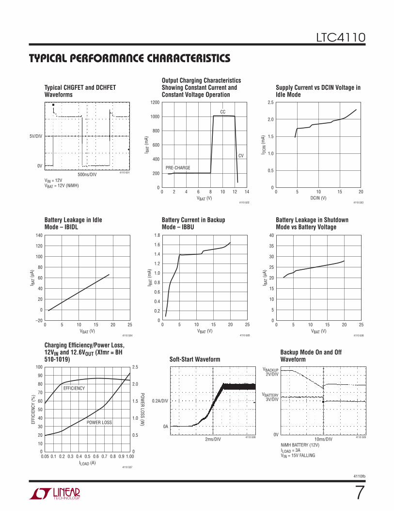
TYPICAL PERFORMANCE CHARACTERISTICS
Typical CHGFET and DCHFET Waveforms
Output Charging Characteristics Showing Constant Current and Constant Voltage Operation
Supply Current vs DCIN Voltage in Idle Mode
Battery Leakage in Idle Mode – IBIDL
Battery Current in Backup Mode – IBBU
Battery Leakage in Shutdown Mode vs Battery Voltage
Charging Effi ciency/Power Loss, 12VIN and 12.6VOUT (Xfmr = BH 510-1019) Soft-Start Waveform
Backup Mode On and Off Waveform
4110 G05
0 5 10 15 2520
VBAT (V)
I BA
T (
mA
)
1.8
1.6
1.4
1.2
1.0
0.8
0.6
0
0.4
0.2
4110 G082ms/DIV
0.2A/DIV
0A
4110 G0910ms/DIV
NiMH BATTERY (12V)ILOAD = 3AVIN = 15V FALLING
VBATTERY3V/DIV
VBACKUP2V/DIV
0V
LTC4110
84110fb
PIN FUNCTIONSDCIN (Pin 1): External DC Power Sense Input. Provides a control input and supply for the main supply ideal diode function.
CLN (Pin 2): Current Limit Sense Negative Input. See CLP pin.
CLP (Pin 3): Current Limit Sense Positive Input. This pin and the CLN pin form a differential input that senses volt-age on an external resistor for reverse current entering the power source while in low loss calibration mode. Should the current approach reversal, this function will terminate calibration. An RC fi lter may be required to fi lter out system load noise. Connect both CLP and CLN pins to GND to disable this function. A differential voltage of >1V between the CLP and CLN pins may damage the device.
ACPDLY (Pin 4): ACPb Delay Control Pin. A capacitor connected from ACPDLY to GND and a resistor from VREF to GND programs delay in the ACPb pin high-to-low transition. Open if minimum delay is desired.
DCDIV (Pin 5): AC Present Detection Input. Backup operation is invoked when the system power voltage, divided by an external resistor divider, falls below the threshold of this pin.
SHDN (Pin 6): Active High Shutdown/Reset Control Logic Input. Forces micropower shutdown mode if high when DCIN supply is removed. Forces all registers to reset if high when DCIN supply is present. Normally tied to ground. Internal pin pull-up current.
SDA (Pin 7): SMBus Bidirectional Data Signal. Connect to VDD when not in use.
SCL (Pin 8): SMBus Clock Signal Input From SMBus Host. Connect to VDD when not in use.
GPIO1 (Pin 9): General Purpose I/O or Charge Status Pin. A logic-level I/O bit port that is confi gurable as a host-driven input/output port or as a battery charge status output (CHGb) with an open-drain N-MOSFET that is asserted low when any
smart battery or Li-Ion battery is in any phase of charging or when lead acid battery charge current is >C/x where:
xC
ICHG= • 5
(See C/x Charge Termination section for more details). If the No SMBus option is selected with the SELA pin, the GPIO1 pin defaults as battery charge status. Refer to Table 5a.
GPIO2 (Pin 10): General Purpose I/O Pin. A logic-level I/O bit port that is confi gurable as a host-driven input/output port or as a battery undervoltage status output (BKUP_FLTb) with an open-drain N-MOSFET that is asserted low only while in backup mode if the battery’s average cell voltage drops below voltage programmed by the VDIS pin. If the No SMBus option is selected with the SELA pin, then the GPIO2 pin defaults as battery undervoltage status. Refer to Table 5c.
GPIO3 (Pin 11): General Purpose I/O Pin. A logic-level I/O bit port that is confi gurable as a host-driven input/output port or as a calibration complete status output (CAL_COM-PLETEb) with an open-drain N-MOSFET that is asserted low when calibration has been completed. If the SELA pin is programmed for no SMBus use then the status output is charge fault (CHGFLTb) instead of calibration complete. Refer to Table 5e.
SELA (Pin 12): SMBus Address Selection Input. Selects the LTC4110 SMBus address to facilitate redundant backup systems when standard batteries are used. Connect to GND for 12h, VDD for 28h and the VREF pin for 20h. When a smart battery is selected by the TYPE pin, the SELA pin must be connected to GND to select address 12h. If the SMBus is not used or to force all GPIOs to status mode upon power-up, connect pin to a typically 0.5 • VREF volt-age from VREF pin resistor divider. The SMBus address, if used, will be 12h.
LTC4110
94110fb
ACPb (Pin 13): AC Present Status Digital Output. Open-Drain N-MOSFET output is asserted low when the main supply is present as detected by the DCDIV pin and internal DCIN UVLO.
VDIS (Pin 14): Battery Discharge Voltage Limit During Backup Program Input. Battery threshold voltage at which backup mode will terminate by turning off the isolation P-MOSFET with the BATID pin. Adjustable from external resistor string biased from VREF pin. For default threshold connect to GND pin.
VCAL (Pin 15): Battery Voltage Limit During Calibra-tion Program Input. Battery threshold voltage at which calibration will terminate. Adjustable from external resistor string biased from VREF pin. For default threshold connect to GND pin.
VCHG (Pin 16): Battery Float Voltage Program Input. Trims the fl oat voltage during charging. Programmed from external resistor string biased from VREF pin. Connect to GND for default fl oat voltage.
VREF (Pin 17): Voltage Reference Output and Timing Pro-gramming Input. Provides a typical virtual reference of 1.220V (VREF) for an external resistor divider tied between this pin and GND that programs the VCHG, VCAL and VDIS pin functions. Total resistance from VREF to GND, along with the capacitor on the timer pin, programs the charge time. Voltage refer-ence output remains active in all modes except shutdown. Load current must be between 10μA and 25μA.
TIMER (Pin 18): Charge Timing Input. A capacitor con-nected between TIMER and GND along with the resistance connected from VREF to GND programs the charge time intervals.
TYPE (Pin 19): Refer to Table 8.
THA (Pin 20): SafetySignal Force/Sense Pin to Smart Battery and Force Pin to Lead Acid Battery Thermistor. See description of operation for more detail. The maxi-mum allowed combined capacitance on THA, THB and SafetySignal is 1nF. For lead acid battery applications the maximum capacitance on the THA pin is 50pF.
THB (Pin 21): SafetySignal Force/Sense Pin to Smart Battery and Sense Pin to Lead Acid Battery Thermistor. See description of operation for more detail. The maxi-mum allowed combined capacitance on THA, THB and SafetySignal is 1nF.
IPCC (Pin 22): Battery Preconditioning Charge Current Program Input. Programs the battery current during preconditioning or wakeup charging. Programmed from external resistor to GND.
ICAL (Pin 23): Battery Discharge Current During Calibration Program Input. Programs the constant discharge current at the battery during calibration. Programmed from external resistor to GND.
ICHG (Pin 24): Battery Current During Charge Program Input. Programs the battery current while constant-current bulk charging. Programmed from external resistor to GND.
ITH (Pin 25): Control Signal of the Current Mode PWM. AC compensates control loop. Higher ITH voltage corresponds to higher charging current.
CSP (Pin 26): Current Sense Positive Input. This pin and the CSN pin measure voltage across the external current sense resistor to control battery current during charging and calibration.
CSN (Pin 27): Current Sense Negative Input. This pin and the CSP pin measure voltage across the external current sense resistor to control battery current during charging and calibration.
SGND (Pin 28): Signal Ground Reference Input. This pin should be Kelvin connected to the fl yback current sense resistor and to the battery return.
ISENSE (Pin 29): Current Sense Input. Senses current in the fl yback transformer by monitoring voltage across the external current sense resistor. This pin should be Kelvin-connected to the resistor.
SELC (Pin 30): Refer to Table 8.
PIN FUNCTIONS
LTC4110
104110fb
BAT (Pin 31): Battery Voltage Sense Input. This pin is used to monitor the battery and control charging voltage through an internal resistor divider connected to this pin that is disconnected in shutdown mode. Also provides a control input for battery ideal diode functions. Pin should be Kelvin-connected to battery to avoid voltage drop errors.
DCHFET (Pin 32): Drives the Gate of an External N-MOSFET. Used to drive energy into the battery side of the high ef-fi ciency switch mode converter during low loss calibration discharge of the battery. Provides synchronous rectifi cation during battery charging.
CHGFET (Pin 33): Drives the Gate of an External N-MOSFET. Used to drive energy into the supply side of the high effi ciency switch mode converter during battery charging. Provides synchronous rectifi cation during low loss calibration mode.
VDD (Pin 34): Bypass Capacitor Connection for Internal VDD Regulator. Bypass at pin with 100nF low ESR capaci-tor to GND.
BATID (Pin 35): Drives the Gate of the Battery P-MOSFET Ideal Diode. Controls low loss ideal diode between the battery and backup load when in backup mode. When not in backup mode, the P-MOSFET is turned off to prevent battery power from back driving into main power.
NC (Pin 36): No Connect.
DCOUT (Pin 37): System Power Output Voltage Monitor Input. Provides a control input for supply input ideal diode and battery ideal diode functions. Also supplies power to the IC. Bypass at pin with 100nF low ESR capacitor to GND.
INID (Pin 38): Drives the Gate of the Supply Input P-MOSFET Ideal Diode. Controls low loss ideal diode between the sup-ply input and backup load when not in backup mode.
Exposed Pad (Pin 39): Ground. The Exposed Pad must be soldered to the PCB.
PIN FUNCTIONS
LTC4110
114110fb
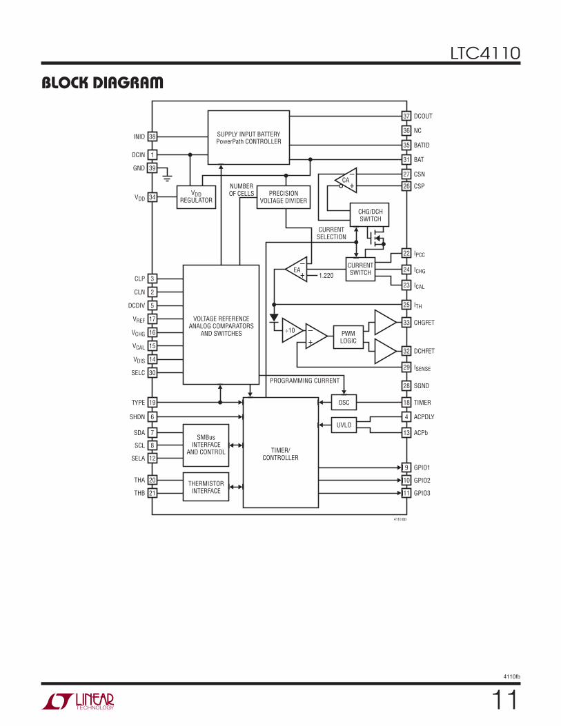
BLOCK DIAGRAM
–
+
–
+
–
+
SUPPLY INPUT BATTERYPowerPath CONTROLLER
VOLTAGE REFERENCEANALOG COMPARATORS
AND SWITCHES
THERMISTORINTERFACE
SMBusINTERFACE
AND CONTROL TIMER/CONTROLLER
UVLO
PWMLOGIC
CURRENTSWITCH
CHG/DCHSWITCH
NUMBEROF CELLS
CURRENTSELECTION
PROGRAMMING CURRENT
PRECISIONVOLTAGE DIVIDER
VDDREGULATOR
EA
÷10
CA
OSC
1.220
38INID
1DCIN
39GND
34VDD
3CLP
2CLN
5DCDIV
17VREF
16VCHG
15VCAL
14VDIS
30SELC
19TYPE
6SHDN
7SDA
8SCL
12SELA
20THA
21THB
10 GPIO2
9 GPIO1
11 GPIO3
13 ACPb
4 ACPDLY
18 TIMER
28 SGND
29 ISENSE
32 DCHFET
33 CHGFET
25 ITH
23 ICAL
24 ICHG
22 IPCC
26 CSP
27 CSN
31 BAT
35 BATID
36 NC
37 DCOUT
4110 BD
LTC4110
124110fb
OVERVIEW
In the typical application, the LTC4110 is placed in series with main power supply that powers all or part of the system, which must include the device(s) or system that needs battery backup.
The LTC4110 has four modes of operation:
• Battery Backup Mode
• Battery Charge Mode
• Battery Calibration Mode
• Shutdown Mode
The LTC4110 provides complete PowerPath control for the battery backed up load switching automatically from the main power supply to the battery when battery backup mode is required. Low loss ideal diode FET switches are used to connect the main supply or the battery to the backup load which permit multiple LTC4110’s to work together in a scalable fashion to permit longer backup times, redundancy and/or higher load currents. In battery charge mode, power is drawn from the main supply by a high effi ciency synchronous fl yback charger. The LTC4110 maintains the state of charge (SOC) of the battery at all times so the battery is ready at all times. Use of a fl yback converter permits charging of batteries who’s termination voltage can be greater than the main supply voltage, while at the same time providing high DC isolation to minimize parasitic drain on the battery. Testing, maintenance support and capacity verifi cation of the battery is supported through the LTC4110’s calibration mode. In calibration mode, the same synchronous fl yback used to charge the battery is
OPERATIONalso used in reverse to allow safe controlled discharge of the battery back into the main supply eliminating wasted heat and energy. The product will not need to provide any additional thermal management to support this mode. Shutdown mode disconnects the battery from the load to preserve capacity and permits shipping the product with an energized battery installed at the factory, eliminating battery installation at the site. The LTC4110 supports optional control and monitoring of all activities by a host including faults over the industry standard SMBus, which is a variation of the I2C bus. However no host is required as the LTC4110 is fully functional in a standalone mode. Combining all these functions into a single IC reduces circuit area compared to presently available solutions.
The LTC4110 is designed to work with both standard battery and smart battery confi gurations. Smart batteries are standard batteries with industry standard gas gauge electronics built in offering accurate SOC information for the host. Furthermore, being intimate with all aspects of the battery, it also has the ability to control the charge process. Smart batteries use the SMBus as the com-munication bus for data exchange and charge control. For more information about smart batteries, see www.sbs-forum.org for specifi cations or contact Linear Tech-nology Applications.
It is important to know that the LTC4110 uses the TYPE pin to learn what type of battery it will be working with. The TYPE pin setting globally affects all of the operating modes, options including GPIO and control ranges. Table 1 and Table 2 give you a complete breakdown of all the battery types supported relative to the TYPE pin settings
Table 1. LTC4110 Battery Pack Charge Mode Capabilities
BATTERY TYPE CHEMISTRY MAXIMUM CHARGE TIME (SLA EXCLUDED)
Li-Ion/Polymer Nickel SLA/Lead Acid
Standard Battery Yes No Yes Adj. Up to 12 Hours
Smart Battery Yes Yes Yes Unlimited
Table 2. LTC4110 Battery Pack Charge Voltage Capabilities
CHEMISTRY VCELL FULL CHARGE VCELL ADJ. RANGE SERIES CELL COUNT NOMINAL STACK VOLTAGE (V)
Lead Acid 2.35V ±0.15V 2, 3, 5 and 6 4, 6, 10 and 12
Li-Ion/Polymer 4.2V ±0.3V 1, 2, 3 and 4 3.6, 7.2, 10.8 and 14.4
NiMH/NiCd N/A N/A 4, 6, 9 and 10 4.8, 7.2, 10.8 and 12
Super Caps 2.5V, 2.7V or 3V Yes 2 to 7 5 to 18
LTC4110
134110fb
and ranges. It should be noted that even if the LTC4110 TYPE pin is not set to a smart battery mode, any SMBus commands sent by a host or a smart battery are still acted upon. For SuperCap support, see the Applications Information section.
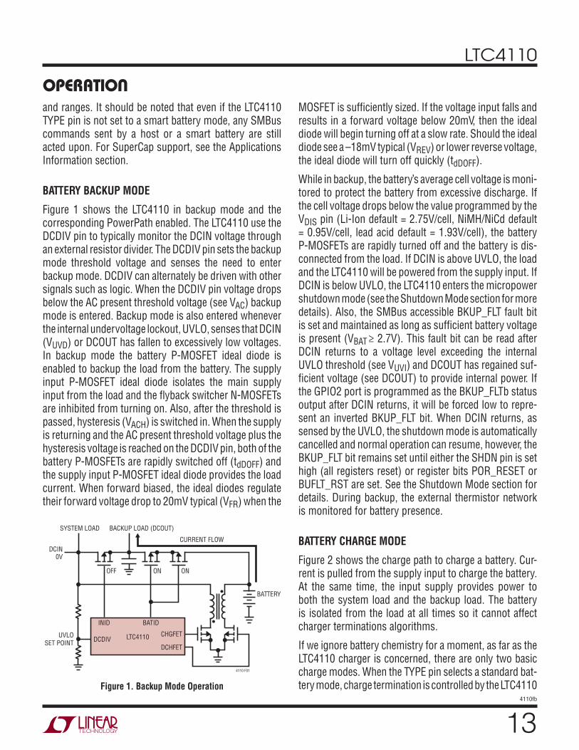
BATTERY BACKUP MODE
Figure 1 shows the LTC4110 in backup mode and the corresponding PowerPath enabled. The LTC4110 use the DCDIV pin to typically monitor the DCIN voltage through an external resistor divider. The DCDIV pin sets the backup mode threshold voltage and senses the need to enter backup mode. DCDIV can alternately be driven with other signals such as logic. When the DCDIV pin voltage drops below the AC present threshold voltage (see VAC) backup mode is entered. Backup mode is also entered whenever the internal undervoltage lockout, UVLO, senses that DCIN (VUVD) or DCOUT has fallen to excessively low voltages. In backup mode the battery P-MOSFET ideal diode is enabled to backup the load from the battery. The supply input P-MOSFET ideal diode isolates the main supply input from the load and the fl yback switcher N-MOSFETs are inhibited from turning on. Also, after the threshold is passed, hysteresis (VACH) is switched in. When the supply is returning and the AC present threshold voltage plus the hysteresis voltage is reached on the DCDIV pin, both of the battery P-MOSFETs are rapidly switched off (tdDOFF) and the supply input P-MOSFET ideal diode provides the load current. When forward biased, the ideal diodes regulate their forward voltage drop to 20mV typical (VFR) when the
MOSFET is suffi ciently sized. If the voltage input falls and results in a forward voltage below 20mV, then the ideal diode will begin turning off at a slow rate. Should the ideal diode see a –18mV typical (VREV) or lower reverse voltage, the ideal diode will turn off quickly (tdDOFF).
While in backup, the battery’s average cell voltage is moni-tored to protect the battery from excessive discharge. If the cell voltage drops below the value programmed by the VDIS pin (Li-Ion default = 2.75V/cell, NiMH/NiCd default = 0.95V/cell, lead acid default = 1.93V/cell), the battery P-MOSFETs are rapidly turned off and the battery is dis-connected from the load. If DCIN is above UVLO, the load and the LTC4110 will be powered from the supply input. If DCIN is below UVLO, the LTC4110 enters the micropower shutdown mode (see the Shutdown Mode section for more details). Also, the SMBus accessible BKUP_FLT fault bit is set and maintained as long as suffi cient battery voltage is present (VBAT ≥ 2.7V). This fault bit can be read after DCIN returns to a voltage level exceeding the internal UVLO threshold (see VUVI) and DCOUT has regained suf-fi cient voltage (see DCOUT) to provide internal power. If the GPIO2 port is programmed as the BKUP_FLTb status output after DCIN returns, it will be forced low to repre-sent an inverted BKUP_FLT bit. When DCIN returns, as sensed by the UVLO, the shutdown mode is automatically cancelled and normal operation can resume, however, the BKUP_FLT bit remains set until either the SHDN pin is set high (all registers reset) or register bits POR_RESET or BUFLT_RST are set. See the Shutdown Mode section for details. During backup, the external thermistor network is monitored for battery presence.
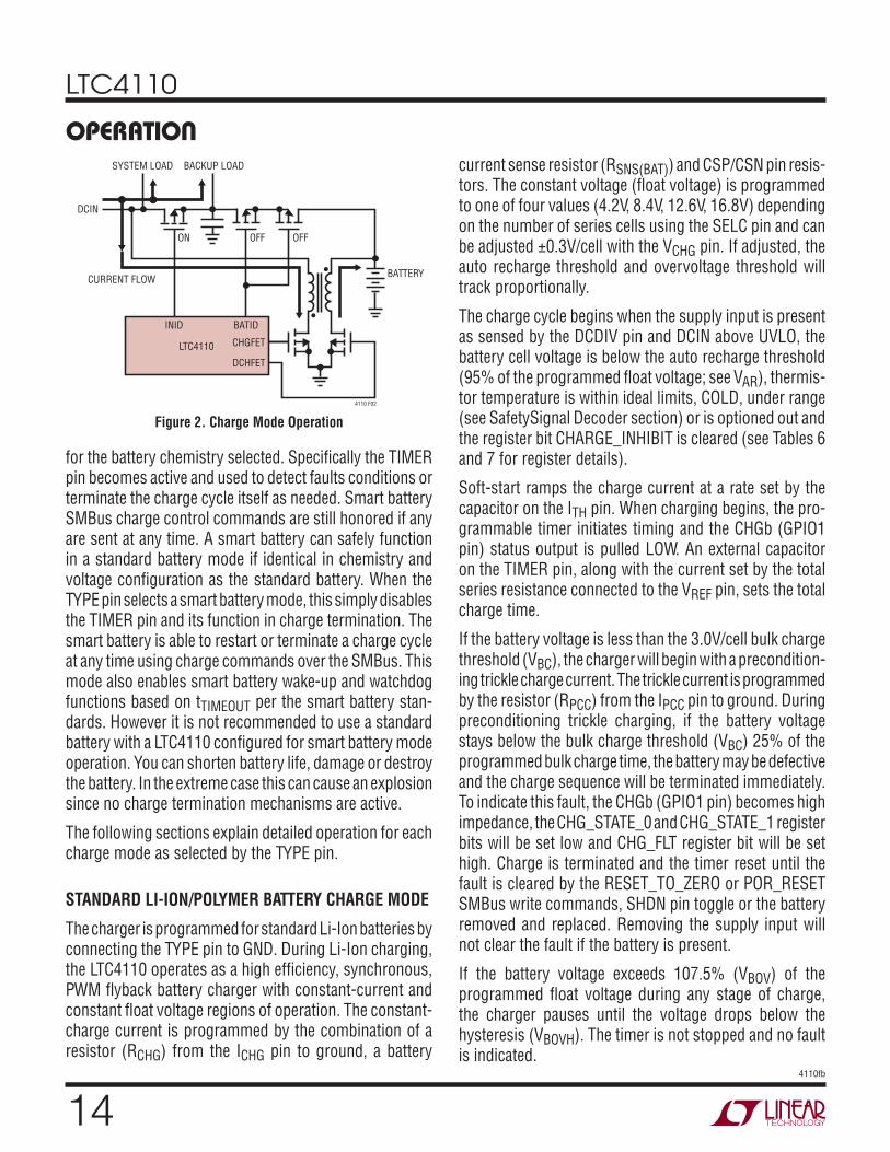
BATTERY CHARGE MODE
Figure 2 shows the charge path to charge a battery. Cur-rent is pulled from the supply input to charge the battery. At the same time, the input supply provides power to both the system load and the backup load. The battery is isolated from the load at all times so it cannot affect charger terminations algorithms.
If we ignore battery chemistry for a moment, as far as the LTC4110 charger is concerned, there are only two basic charge modes. When the TYPE pin selects a standard bat-tery mode, charge termination is controlled by the LTC4110
OPERATION
Figure 1. Backup Mode Operation
LTC4110
INID BATID
DCDIV
DCHFET
CHGFETUVLO
SET POINT
BACKUP LOAD (DCOUT)
CURRENT FLOW
SYSTEM LOAD
BATTERY
DCIN0V
ON ONOFF
4110 F01
LTC4110
144110fb
for the battery chemistry selected. Specifi cally the TIMER pin becomes active and used to detect faults conditions or terminate the charge cycle itself as needed. Smart battery SMBus charge control commands are still honored if any are sent at any time. A smart battery can safely function in a standard battery mode if identical in chemistry and voltage confi guration as the standard battery. When the TYPE pin selects a smart battery mode, this simply disables the TIMER pin and its function in charge termination. The smart battery is able to restart or terminate a charge cycle at any time using charge commands over the SMBus. This mode also enables smart battery wake-up and watchdog functions based on tTIMEOUT per the smart battery stan-dards. However it is not recommended to use a standard battery with a LTC4110 confi gured for smart battery mode operation. You can shorten battery life, damage or destroy the battery. In the extreme case this can cause an explosion since no charge termination mechanisms are active.
The following sections explain detailed operation for each charge mode as selected by the TYPE pin.
STANDARD LI-ION/POLYMER BATTERY CHARGE MODE
The charger is programmed for standard Li-Ion batteries by connecting the TYPE pin to GND. During Li-Ion charging, the LTC4110 operates as a high effi ciency, synchronous, PWM fl yback battery charger with constant-current and constant fl oat voltage regions of operation. The constant-charge current is programmed by the combination of a resistor (RCHG) from the ICHG pin to ground, a battery
OPERATIONcurrent sense resistor (RSNS(BAT)) and CSP/CSN pin resis-tors. The constant voltage (fl oat voltage) is programmed to one of four values (4.2V, 8.4V, 12.6V, 16.8V) depending on the number of series cells using the SELC pin and can be adjusted ±0.3V/cell with the VCHG pin. If adjusted, the auto recharge threshold and overvoltage threshold will track proportionally.
The charge cycle begins when the supply input is present as sensed by the DCDIV pin and DCIN above UVLO, the battery cell voltage is below the auto recharge threshold (95% of the programmed fl oat voltage; see VAR), thermis-tor temperature is within ideal limits, COLD, under range (see SafetySignal Decoder section) or is optioned out and the register bit CHARGE_INHIBIT is cleared (see Tables 6 and 7 for register details).
Soft-start ramps the charge current at a rate set by the capacitor on the ITH pin. When charging begins, the pro-grammable timer initiates timing and the CHGb (GPIO1 pin) status output is pulled LOW. An external capacitor on the TIMER pin, along with the current set by the total series resistance connected to the VREF pin, sets the total charge time.
If the battery voltage is less than the 3.0V/cell bulk charge threshold (VBC), the charger will begin with a precondition-ing trickle charge current. The trickle current is programmed by the resistor (RPCC) from the IPCC pin to ground. During preconditioning trickle charging, if the battery voltage stays below the bulk charge threshold (VBC) 25% of the programmed bulk charge time, the battery may be defective and the charge sequence will be terminated immediately. To indicate this fault, the CHGb (GPIO1 pin) becomes high impedance, the CHG_STATE_0 and CHG_STATE_1 register bits will be set low and CHG_FLT register bit will be set high. Charge is terminated and the timer reset until the fault is cleared by the RESET_TO_ZERO or POR_RESET SMBus write commands, SHDN pin toggle or the battery removed and replaced. Removing the supply input will not clear the fault if the battery is present.
If the battery voltage exceeds 107.5% (VBOV) of the programmed fl oat voltage during any stage of charge, the charger pauses until the voltage drops below the hysteresis (VBOVH). The timer is not stopped and no fault is indicated.
Figure 2. Charge Mode Operation
LTC4110
BACKUP LOADSYSTEM LOAD
BATTERY
OFF OFFON
4110 F02
DCIN
CURRENT FLOW
INID BATID
DCHFET
CHGFET
LTC4110
154110fb
OPERATION
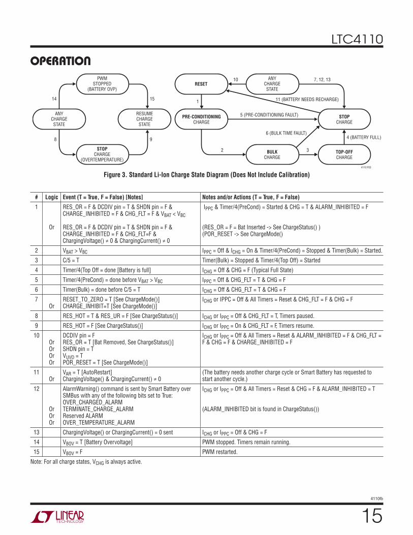
Figure 3. Standard Li-Ion Charge State Diagram (Does Not Include Calibration)
# Logic Event (T = True, F = False) [Notes] Notes and/or Actions (T = True, F = False)
1
Or
RES_OR = F & DCDIV pin = T & SHDN pin = F & CHARGE_INHIBITED = F & CHG_FLT = F & VBAT < VBC
RES_OR = F & DCDIV pin = T & SHDN pin = F & CHARGE_INHIBITED = F & CHG_FLT=F & ChargingVoltage() ≠ 0 & ChargingCurrent() ≠ 0
IPPC & Timer/4(PreCond) = Started & CHG = T & ALARM_INHIBITED = F
(RES_OR = F = Bat Inserted -> See ChargeStatus() )(POR_RESET -> See ChargeMode()
2 VBAT > VBC IPPC = Off & ICHG = On & Timer/4(PreCond) = Stopped & Timer(Bulk) = Started.
3 C/5 = T Timer(Bulk) = Stopped & Timer/4(Top Off) = Started
4 Timer/4(Top Off = done [Battery is full] ICHG = Off & CHG = F (Typical Full State)
5 Timer/4(PreCond) = done before VBAT > VBC IPPC = Off & CHG_FLT = T & CHG = F
6 Timer(Bulk) = done before C/5 = T ICHG = Off & CHG_FLT = T & CHG = F
7Or
RESET_TO_ZERO = T [See ChargeMode()]CHARGE_INHIBIT=T [See ChargeMode()]
ICHG or IPPC = Off & All Timers = Reset & CHG_FLT = F & CHG = F
8 RES_HOT = T & RES_UR = F [See ChargeStatus()] ICHG or IPPC = Off & CHG_FLT = T, Timers paused.
9 RES_HOT = F [See ChargeStatus()] ICHG or IPPC = On & CHG_FLT = F, Timers resume.
10OrOrOrOr
DCDIV pin = FRES_OR = T [Bat Removed, See ChargeStatus()]SHDN pin = TVUVD = TPOR_RESET = T [See ChargeMode()]
ICHG or IPPC = Off & All Timers = Reset & ALARM_INHIBITED = F & CHG_FLT = F & CHG = F & CHARGE_INHIBITED = F
11Or
VAR = T [AutoRestart]ChargingVoltage() & ChargingCurrent() ≠ 0
(The battery needs another charge cycle or Smart Battery has requested to start another cycle.)
12
OrOrOr
AlarmWarning() command is sent by Smart Battery over SMBus with any of the following bits set to True: OVER_CHARGED_ALARMTERMINATE_CHARGE_ALARMReserved ALARMOVER_TEMPERATURE_ALARM
ICHG or IPPC = Off & All Timers = Reset & CHG = F & ALARM_INHIBITED = T
(ALARM_INHIBITED bit is found in ChargeStatus())
13 ChargingVoltage() or ChargingCurrent() = 0 sent ICHG or IPPC = Off & CHG = F
14 VBOV = T [Battery Overvoltage] PWM stopped. Timers remain running.
15 VBOV = F PWM restarted.
Note: For all charge states, VCHG is always active.
4110 F03
PWMSTOPPED
(BATTERY OVP)
STOPCHARGE
(OVERTEMPERATURE)
ANYCHARGESTATE
RESUMECHARGESTATE
15
9
14
8
ANYCHARGESTATE
PRE-CONDITIONINGCHARGE
STOPCHARGE
TOP-OFFCHARGE
7, 12, 1310
4 (BATTERY FULL)
1
2 3
RESET
5 (PRE-CONDITIONING FAULT)
11 (BATTERY NEEDS RECHARGE)
6 (BULK TIME FAULT)
BULKCHARGE
LTC4110
164110fb
When the battery voltage exceeds the bulk charge threshold (VBC), the charger begins the bulk charge portion of the charge cycle. As the battery accepts charge, the voltage increases. Constant-current charge continues until the battery approaches the constant voltage. At this time, the charge current will begin to drop, signaling the beginning of the constant-voltage portion of the charge cycle.
The charger will maintain the constant voltage across the bat-tery until either C/x is reached or 100% of the programmed bulk charge time has elapsed during bulk charge. When the current drops to approximately 20% of the full-scale charge current, an internal C/x comparator will initiate the start of the top-off stage. The top-off stage charges for 25% of the total programmed bulk charge time. When the time elapses, charge is terminated and CHGb (GPIO1 pin) is forced to a high impedance state and CHG_STATE_0 and CHG_STATE_1 register bits will be set low. Should the total bulk charge time elapse before C/x is reached, charge is terminated and a CHG_FLT fault is indicated until cleared by the RESET_TO_ZERO or POR_RESET SMBus write commands, SHDN pin toggle or the battery removed and replaced. Fault conditions are not cleared when the supply input is removed if the battery has suffi cient voltage.
An optional external thermistor network is sampled at regular intervals to monitor battery temperature and to detect battery presence. If the thermistor temperature is hot (see the SafetySignal Decoder section), the charge timer is paused, charge current is halted, CHG_FLTb (GPIO3 pin) is forced low and the CHG_FLT bit will be set high. CHGb (GPIO1 pin) , CHG_STATE_0 and CHG_STATE_1 register bits will not be affected. When the thermistor value returns to an acceptable value, charging resumes, CHG_FLTb (GPIO3 pin) returns to high impedance and the CHG_FLT bit will be reset low. An open thermistor indicates absence of a battery. To defeat the temperature monitoring function, replace the thermistor with a resistor to indicate ideal battery temperature. When a thermistor is not used, the resistor circuit must be routed through the battery connector if battery presence detection is required.
After a charge cycle has ended without fault, the charge cycle is automatically restarted if the average battery cell voltage falls below the auto recharge threshold. At any
time charging can be forced to stop by pulling the SHDN pin high or setting the CHARGE_INHIBIT bit high through the SMBus.
SMART BATTERY CHARGE MODE
This section explains operation for smart batteries with a SMBus interface. Smart Li-Ion is selected by connecting the TYPE pin to the VDD pin and smart Nickel (NiMH/NiCd) is selected by connecting the TYPE pin to the VREF pin. The LTC4110 only implements a subset of smart battery charger commands; the actual charging algorithm is determined by LTC4110 through external resistors even if the battery is “smart.”
The LTC4110 operates as a high effi ciency, synchronous, PWM fl yback battery charger with constant current and constant fl oat voltage regions of operation. The constant-charge current is programmed by the combination of a resistor (RCHG) from the ICHG pin to ground, a battery current sense resistor (RSNS(BAT)) and CSP/CSN pin resistors. For Li-Ion the constant voltage (fl oat voltage) is programmed to one of four values (4.2V, 8.4V, 12.6V, 16.8V) depending on the number of series cells using the SELC pin and can be adjusted ±0.3V/cell with the VCHG pin. For nickel batteries the constant-voltage function is not used, however, a non-zero value is still required to be written to the ChargingVoltage() register. The internal auto recharge function is inhibited for smart batteries.
If the battery voltage exceeds 107.5% (VBOV) of the programmed fl oat voltage during any stage of charge, the charger pauses until the voltage drops below the hysteresis (VBOVH). The timer is not stopped and no fault is indicated. This function is disabled when nickel based smart batteries are used.
There are four states associated with smart battery charge mode, namely:
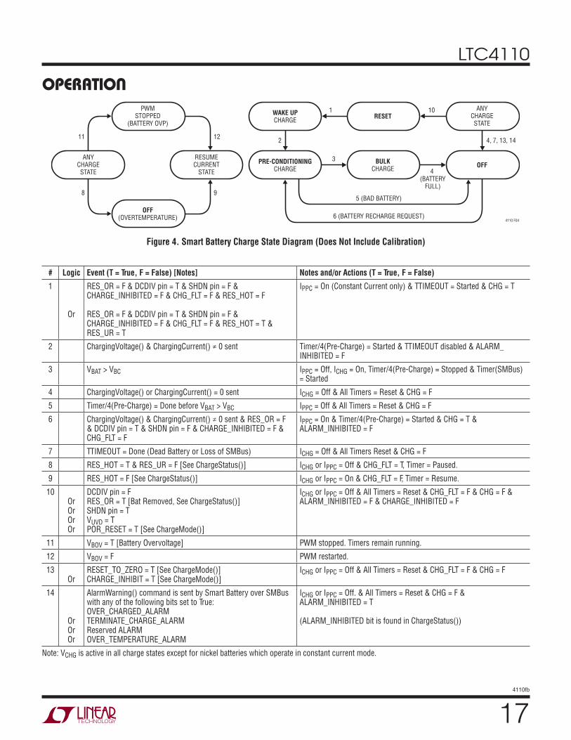
• SMBus Wake-Up Charge State • SMBus Preconditioning Charge State • SMBus Bulk Charge State • SMBus OFF State These states are explained in the following four sections.
OPERATION
LTC4110
174110fb
OPERATION
Figure 4. Smart Battery Charge State Diagram (Does Not Include Calibration)
# Logic Event (T = True, F = False) [Notes] Notes and/or Actions (T = True, F = False)
1
Or
RES_OR = F & DCDIV pin = T & SHDN pin = F & CHARGE_INHIBITED = F & CHG_FLT = F & RES_HOT = F
RES_OR = F & DCDIV pin = T & SHDN pin = F & CHARGE_INHIBITED = F & CHG_FLT = F & RES_HOT = T & RES_UR = T
IPPC = On (Constant Current only) & TTIMEOUT = Started & CHG = T
2 ChargingVoltage() & ChargingCurrent() ≠ 0 sent Timer/4(Pre-Charge) = Started & TTIMEOUT disabled & ALARM_INHIBITED = F
3 VBAT > VBC IPPC = Off, ICHG = On, Timer/4(Pre-Charge) = Stopped & Timer(SMBus) = Started
4 ChargingVoltage() or ChargingCurrent() = 0 sent ICHG = Off & All Timers = Reset & CHG = F
5 Timer/4(Pre-Charge) = Done before VBAT > VBC IPPC = Off & All Timers = Reset & CHG = F
6 ChargingVoltage() & ChargingCurrent() ≠ 0 sent & RES_OR = F & DCDIV pin = T & SHDN pin = F & CHARGE_INHIBITED = F & CHG_FLT = F
IPPC = On & Timer/4(Pre-Charge) = Started & CHG = T & ALARM_INHIBITED = F
7 TTIMEOUT = Done (Dead Battery or Loss of SMBus) ICHG = Off & All Timers Reset & CHG = F
8 RES_HOT = T & RES_UR = F [See ChargeStatus()] ICHG or IPPC = Off & CHG_FLT = T, Timer = Paused.
9 RES_HOT = F [See ChargeStatus()] ICHG or IPPC = On & CHG_FLT = F, Timer = Resume.
10OrOrOrOr
DCDIV pin = FRES_OR = T [Bat Removed, See ChargeStatus()]SHDN pin = TVUVD = TPOR_RESET = T [See ChargeMode()]
ICHG or IPPC = Off & All Timers = Reset & CHG_FLT = F & CHG = F & ALARM_INHIBITED = F & CHARGE_INHIBITED = F
11 VBOV = T [Battery Overvoltage] PWM stopped. Timers remain running.
12 VBOV = F PWM restarted.
13Or
RESET_TO_ZERO = T [See ChargeMode()]CHARGE_INHIBIT = T [See ChargeMode()]
ICHG or IPPC = Off & All Timers = Reset & CHG_FLT = F & CHG = F
14
OrOrOr
AlarmWarning() command is sent by Smart Battery over SMBus with any of the following bits set to True: OVER_CHARGED_ALARMTERMINATE_CHARGE_ALARMReserved ALARMOVER_TEMPERATURE_ALARM
ICHG or IPPC = Off. & All Timers = Reset & CHG = F & ALARM_INHIBITED = T
(ALARM_INHIBITED bit is found in ChargeStatus())
Note: VCHG is active in all charge states except for nickel batteries which operate in constant current mode.
4110 F04
PWMSTOPPED
(BATTERY OVP)
OFF(OVERTEMPERATURE)
ANYCHARGESTATE
RESUMECURRENT
STATE
12
9
11
8
PRE-CONDITIONINGCHARGE
WAKE UPCHARGE
1
4(BATTERY
FULL)
2 4, 7, 13, 14
3
ANYCHARGESTATE
10RESET
OFF
5 (BAD BATTERY)
6 (BATTERY RECHARGE REQUEST)
BULKCHARGE
LTC4110
184110fb
SMBUS WAKE-UP CHARGE STATE
The battery will be charged with a fi xed “wake-up” current regardless of previous ChargingCurrent() and Charging-Voltage() register values during wake-up charging. The cur-rent is identical to the preconditioning charge current which is programmed with an external resistor through the IPCC pin. The wake-up timer has the same period as tTIMEOUT, typically 175sec (see tTIMEOUT).
The following conditions must be met to allow wake-up charge of the battery:
• The SafetySignal must be RES_COLD, RES_IDEAL, or RES_UR.
• AC must be present. This is qualifi ed by DCDIV > VAC + VACH and DCIN above UVLO.
• Wake-up charge initiates if a battery does not write non-zero values to ChargingCurrent() and Chargin-Voltage() registers when AC power is applied and a battery is present or when AC is present and a battery is subsequently connected.
The following conditions will terminate the wake-up charge state and end charge attempts, unless otherwise noted.
• The tTIMEOUT period is reached (see tTIMEOUT) when the SafetySignal is RES_COLD or RES_UR. The state machine will go to the SMBus OFF state. The CHG_FLT bit is not set.
• The SafetySignal is registering RES_HOT. The state machine will go to the SMBus OFF state.
• The SafetySignal is registering RES_OR. The state machine will go to the reset state.
• The LTC4110 will leave the wake-up charge state and go into the SMBus preconditioning charge state if the ChargingCurrent() AND ChargingVoltage() registers have been written to non-zero values.
• The AC power is no longer present (DCDIV < VAC or DCIN below UVLO). The state machine will go to the reset state.
• The ALARM_INHIBITED becomes set in the ChargerStatus() register. The state machine will go to the SMBus OFF state.
• CHARGE_INHIBIT is set in the BBuControl() register. Charge is stopped, however, the wake-up timer is not paused. Clearing CHARGE_INHIBIT will enable the LTC4110 to resume charging.
• There is insuffi cient DCIN voltage to charge the battery as determined by the internal UVLO. This causes the state machine to enter the reset state and stop all charge activity. The LTC4110 will resume wake-up charging when there is suffi cient DCIN voltage to charge the battery.
• The CAL_START bit in the BBuControl() register is set. Charge is stopped and the LTC4110 enters the calibra-tion state.
• Writing a zero value to either the ChargingVoltage() or ChargingCurrent() register. The state machine will go to the SMBus OFF state.
• RESET_TO_ZERO is set in the BBuControl() register. Charge is stopped; the SMBus OFF State is entered.
SMBUS PRECONDITIONING CHARGE STATE
During the SMBus preconditioning charge state, the charger will be operating in the preconditioning charge current limit. The following conditions must be met in order to allow SMBus preconditioning charge to start:
• The ChargingVoltage() AND ChargingCurrent() registers must be written to non-zero values. The LTC4110 will not directly report the status of these registers. The battery needs only write one pair of ChargingVoltage() and ChargingCurrent() registers to stay in this state. The tTIMEOUT timer is not operational in SMBus precondition-ing charge state.
• The SafetySignal must be RES_COLD, RES_IDEAL, or RES_UR.
• AC must be present and suffi cient. This is qualifi ed by DCDIV > VAC + VACH and DCIN > UVLO.
The following conditions will affect the SMBus precondi-tioning charge state as specifi ed below:
• The SafetySignal is registering RES_HOT. Charge is stopped; the SMBus OFF state is entered.
OPERATION
LTC4110
194110fb
• The SafetySignal is registering RES_OR. Charge is stopped. The LTC4110 enters the reset state.
• The AC power is no longer present (DCDIV < VAC or DCIN < UVLO). The LTC4110 enters the reset state.
• ALARM_INHIBITED is set in the ChargerStatus() register. Charge is stopped. The LTC4110 enters the SMBus OFF state.
• CHARGE_INHIBIT is set in the BBuControl() register. Charge is stopped, however, the T/4 timer is not paused. Clearing CHARGE_INHIBIT will enable the LTC4110 to resume charge.
• RESET_TO_ZERO is set in the BBuControl() register. Charge is stopped. The LTC4110 enters the SMBus OFF state.
• Writing a zero value to ChargeVoltage() or ChargeCur-rent() register. Charge is stopped. The LTC4110 enters the SMBus OFF state.
• If the battery voltage exceeds the bulk charge threshold, the LTC4110 will enter the SMBus bulk charge state.
• If the T/4 timeout occurs, charge is stopped and the LTC4110 enters the SMBus OFF state.
• The CAL_START bit in the BBuControl() register is set. Charge is stopped and the LTC4110 enters the calibration mode.
SMBus BULK CHARGE STATE
The charger will be operating in the bulk charge current limit during the SMBus bulk charge state. The following conditions must be met in order to allow SMBus bulk charge to start:
• The ChargeVoltage() AND ChargeCurrent() registers must be written to non-zero values. The LTC4110 will not directly report the status of these registers.
• The SafetySignal must be RES_COLD, RES_IDEAL, or RES_UR.
• AC must be present and suffi cient. This is qualifi ed by DCDIV > VAC + VACH and DCIN > UVLO.
The following conditions will affect the SMBus bulk charge state as specifi ed below:
OPERATION• The ChargeCurrent() AND ChargeVoltage() registers
have not been written for tTIMEOUT. Charge is stopped and the LTC4110 enters the SMBus OFF state.
• The SafetySignal is registering RES_OR. Charge is stopped and the LTC4110 enters the reset state.
• The SafetySignal is registering RES_HOT. Charge is stopped and the LTC4110 enters the SMBus OFF state.
• The AC power is no longer present (DCDIV < VAC or DCIN < UVLO). Charge is stopped and the LTC4110 enters the reset state.
• ALARM_INHIBITED is set in the ChargerStatus() register. Charge is stopped and the LTC4110 enters the SMBus OFF state.
• CHARGE_INHIBIT is set in the BBuControl() register. Charge is stopped. Clearing CHARGE_INHIBIT will en-able the LTC4110 to resume charge. The tTIMEOUT timer does not pause when CHARGE_INHIBIT is set.
• RESET_TO_ZERO is set in the BBuControl() register. The LTC4110 enters the SMBus OFF state.
• Writing a zero value to the ChargeVoltage() or to the ChargeCurrent() register. Charge is stopped and the LTC4110 enters the SMBus OFF state.
• The CAL_START bit in the BBuControl() register is set. Charge is stopped and the LTC4110 enters the calibra-tion mode.
SMBus OFF STATE
This state is different from the reset state in that all charge is disallowed regardless of the value of the thermistor. The following conditions will affect the SMBus OFF state as specifi ed below:
• The ChargeCurrent() AND ChargeVoltage() regis-ters have both been written to non-zero values, the battery thermistor is registering RES_COLD, RES_IDEAL or RES_UR and CHARGE_INHIBT is clear. The LTC4110 enters the SMBus preconditioning charge state.
LTC4110
204110fb
• The CAL_START bit in the BBuControl() register is set. The LTC4110 enters the calibration state.
• The battery thermistor is registering RES_OR. The LTC4110 enters the reset state.
LEAD ACID BATTERY CHARGE MODE
The charger is programmed for lead acid batteries by con-necting the TYPE pin to a voltage derived from the VREF pin resistor divider of nominally 0.5 • VREF. During charge, the LTC4110 operates as a high effi ciency, synchronous, PWM fl yback battery charger with constant current and constant fl oat voltage regions of operation. The constant-charge current is programmed by the combination of a resistor (RCHG) from the ICHG pin to ground, a battery current sense resistor (RSNS) and CSP/CSN pin resistors. The fl oat voltage is programmed to one of four values (4.7V, 7.05V, 11.75V, 14.1V) depending on the number of series cells (2, 3, 5 or 6) using the SELC pin and can be adjusted ±0.15V/cell with the VCHG pin.
A new charge cycle begins with the charger in the bulk charge current limited state. In this state, the charger is a current source providing a constant charge rate and the CHGb (GPIO1 pin) is forced low. No time limits are placed upon lead acid battery charge. The charger monitors the battery voltage and as it reaches the fl oat voltage the charger begins its fl oat charge. While in fl oat, the charge current diminishes as the battery accepts charge. Float voltage temperature compensation and temperature fault monitoring, if desired, are accomplished with an external thermistor network.
Charge is active when the supply input is present as sensed by the DCDIV pin and DCIN above UVLO, thermistor temperature is ideal according to the thermistor monitor circuit (see SafetySignal Decoder) and the charge register bit CHARGE_INHIBIT is cleared. Soft-start ramps the charge current at a rate set by the capacitor on the ITH pin. When charge begins, the CHGb (GPIO1 pin) status output is forced to GND. At any time charge can be forced to stop by pulling the SHDN pin high or setting the CHARGE_INHIBIT bit high through the SMBus.
If the battery voltage exceeds 107.5% (VBOV) of the pro-grammed fl oat voltage during any stage of charge, the
charger pauses until the voltage drops below the hysteresis (VBOVH). No fault is indicated.
An optional external NTC thermistor network can be used to provide an adjustable negative TC for the fl oat voltage, monitor battery temperature and to detect battery pres-ence. If the thermistor value indicates a hot temperature, voltage falling to VHOT on THB pin, charge current is halted, CHG_FLTb (GPIO3 pin) is forced low and the CHG_FLT bit will be set high. CHGb (GPIO1 pin) and CHG_STATE_0 and CHG_STATE_1 register bits will not be affected. When the thermistor value returns to ideal when the voltage exceeds VHOT +VHOTH on THB pin, charge resumes CHG_FLTb (GPIO3 pin) returns to high impedance and the CHG_FLT bit will be reset low. An open thermistor indicates an over-range which is considered absence of a battery. Low temperature is not monitored. However, since bat-tery removal detection looks at the thermistor for a high resistance (VREM on THB pin), extremely cold temperatures may result in an indication of battery absence. To defeat the temperature monitoring register, replace the thermis-tor with a resistor to indicate normal battery temperature. When a thermistor is not used the resistor circuit must be routed through the battery connector if battery presence detection is required.
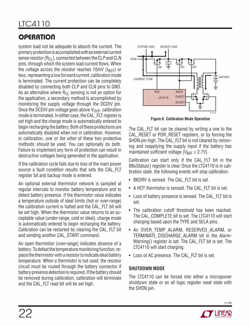
BATTERY CALIBRATION MODE
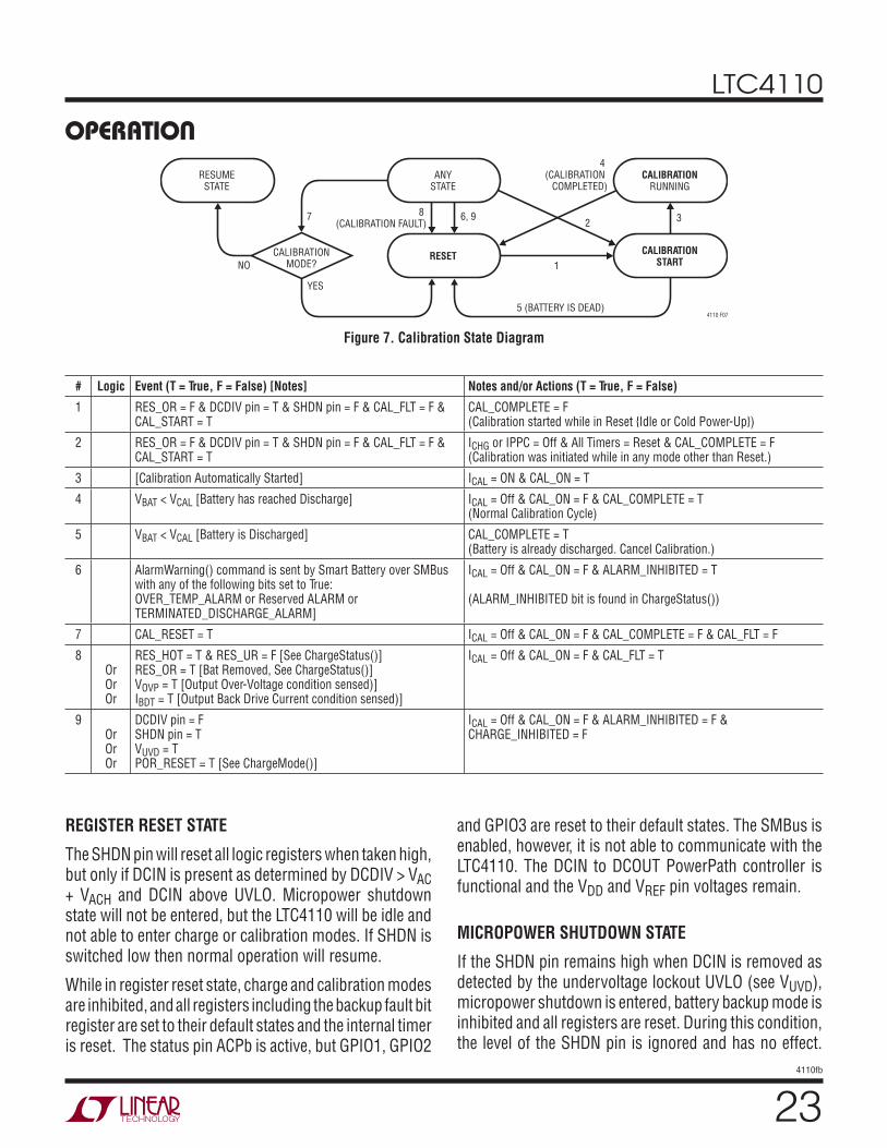
Figure 6 shows the LTC4110 in battery calibration mode and the corresponding PowerPath enabled. During calibration, the host CPU can calibrate a gas gauge or verify the battery’s ability to support a load by use of a low heat producing method. Calibration requires a host to communicate over a SMBus. In the low heat method, a synchronous PWM fl yback charger is used in reverse to discharge the battery with a programmable constant-current into the system load thereby saving space and eliminating heat generation compared with resistive loads. Protection circuits prevent accidental overdrive back into the power source if the system load is insuffi cient. The constant-charge current is programmed by the combination of a resistor (RCAL) from the ICAL pin to ground, a battery current sense resis-tor (RSNS(BAT)) and CSP/CSN pin resistors. Calibration is initiated by setting the CAL_START bit in the BBuControl() register. The CAL_ON bit in the BBuStatus() register will
OPERATION
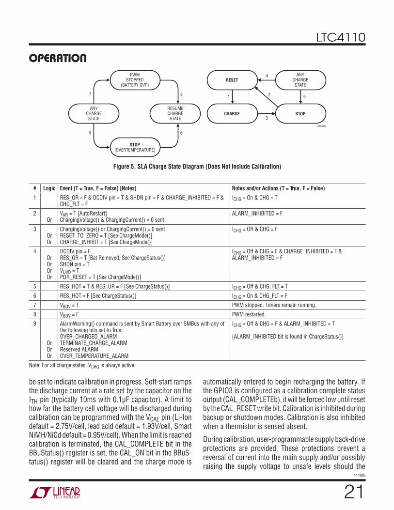
LTC4110
214110fb
OPERATION
be set to indicate calibration in progress. Soft-start ramps the discharge current at a rate set by the capacitor on the ITH pin (typically 10ms with 0.1μF capacitor). A limit to how far the battery cell voltage will be discharged during calibration can be programmed with the VCAL pin (Li-Ion default = 2.75V/cell, lead acid default = 1.93V/cell, Smart NiMH/NiCd default = 0.95V/cell). When the limit is reached calibration is terminated, the CAL_COMPLETE bit in the BBuStatus() register is set, the CAL_ON bit in the BBuS-tatus() register will be cleared and the charge mode is
automatically entered to begin recharging the battery. If the GPIO3 is confi gured as a calibration complete status output (CAL_COMPLETEb), it will be forced low until reset by the CAL_RESET write bit. Calibration is inhibited during backup or shutdown modes. Calibration is also inhibited when a thermistor is sensed absent.
During calibration, user-programmable supply back-drive protections are provided. These protections prevent a reversal of current into the main supply and/or possibly raising the supply voltage to unsafe levels should the
Figure 5. SLA Charge State Diagram (Does Not Include Calibration)
4110 F05
PWMSTOPPED
(BATTERY OVP)
STOP(OVERTEMPERATURE)
ANYCHARGESTATE
RESUMECHARGESTATE
8
6
7
5
3
1 9
ANYCHARGESTATE
4RESET
STOP
2
CHARGE
# Logic Event (T = True, F = False) [Notes] Notes and/or Actions (T = True, F = False)
1 RES_OR = F & DCDIV pin = T & SHDN pin = F & CHARGE_INHIBITED = F & CHG_FLT = F
ICHG = On & CHG = T
2Or
VAR = T [AutoRestart]ChargingVoltage() & ChargingCurrent() ≠ 0 sent
ALARM_INHIBITED = F
3OrOr
ChargingVoltage() or ChargingCurrent() = 0 sentRESET_TO_ZERO = T [See ChargeMode()]CHARGE_INHIBIT = T [See ChargeMode()]
ICHG = Off & CHG = F
4OrOrOrOr
DCDIV pin = FRES_OR = T [Bat Removed, See ChargeStatus()]SHDN pin = TVUVD = TPOR_RESET = T [See ChargeMode()]
ICHG = Off & CHG = F & CHARGE_INHIBITED = F & ALARM_INHIBITED = F
5 RES_HOT = T & RES_UR = F [See ChargeStatus()] ICHG = Off & CHG_FLT = T
6 RES_HOT = F [See ChargeStatus()] ICHG = On & CHG_FLT = F
7 VBOV = T PWM stopped. Timers remain running.
8 VBOV = F PWM restarted.
9
OrOrOr
AlarmWarning() command is sent by Smart Battery over SMBus with any of the following bits set to True: OVER_CHARGED_ALARMTERMINATE_CHARGE_ALARMReserved ALARMOVER_TEMPERATURE_ALARM
ICHG = Off & CHG = F & ALARM_INHIBITED = T
(ALARM_INHIBITED bit is found in ChargeStatus())
Note: For all charge states, VCHG is always active
LTC4110
224110fb
system load not be adequate to absorb the current. The primary protection is accomplished with an external current sense resistor (RCL), connected between the CLP and CLN pins, through which the system load current fl ows. When the voltage across the resistor reaches 10mV (IBDT) or less, representing a low forward current, calibration mode is terminated. The current protection can be completely disabled by connecting both CLP and CLN pins to GND. As an alternative where RCL sensing is not an option for the application, a secondary method is accomplished by monitoring the supply voltage through the DCDIV pin. Once the DCDIV pin voltage goes above VOVP, calibration mode is terminated. In either case, the CAL_FLT register is set high and the charge mode is automatically entered to begin recharging the battery. Both of these protections are automatically disabled when not in calibration. However, in calibration, one or the other of these two protective methods should be used. You can optionally do both. Failure to implement any form of protection can result in destructive voltages being generated in the application.
If the calibration cycle fails due to loss of the main power source a fault condition results that sets the CAL_FLT register bit and backup mode is entered.
An optional external thermistor network is sampled at regular intervals to monitor battery temperature and to detect battery presence. If the thermistor value indicates a temperature outside of ideal limits (hot or over-range) the calibration current is halted and the CAL_FLT bit will be set high. When the thermistor value returns to an ac-ceptable value (under-range, cold or ideal), charge mode is automatically entered to begin recharging the battery. Calibration can be restarted by clearing the CAL_FLT bit and sending another CAL_START command.
An open thermistor (over-range) indicates absence of a battery. To defeat the temperature monitoring function, re-place the thermistor with a resistor to indicate ideal battery temperature. When a thermistor is not used, the resistor circuit must be routed through the battery connector if battery presence detection is required. If the battery should be removed during calibration, calibration will terminate and the CAL_FLT read bit will be set high.
The CAL_FLT bit can be cleared by writing a one to the CAL_RESET or POR_RESET registers, or by forcing the SHDN pin high. The CAL_FLT bit is not cleared by remov-ing and reapplying the supply input if the battery has maintained suffi cient voltage (VBAT ≥ 2.7V).
Calibration can start only if the CAL_FLT bit in the BBuStatus() register is clear. Once the LTC4110 is in cali-bration state, the following events will stop calibration:
• BKDRV is sensed. The CAL_FLT bit is set.
• A HOT thermistor is sensed. The CAL_FLT bit is set.
• Loss of battery presence is sensed. The CAL_FLT bit is set.
• The calibration cutoff threshold has been reached. The CAL_COMPLETE bit is set. The LTC4110 will start charging based upon the TYPE and SELA pins.
• An OVER_TEMP_ALARM, RESERVED_ALARM, or TERMINATE_DISCHARGE_ALARM bit in the Alarm-Warning() register is set. The CAL_FLT bit is set. The LTC4110 will start charging.
• Loss of AC presence. The CAL_FLT bit is set.
SHUTDOWN MODE
The LTC4110 can be forced into either a micropower shutdown state or an all logic register reset state with the SHDN pin.
OPERATION
Figure 6. Calibration Mode Operation
LTC4110
BATTERY
OFF OFFON
4110 F06
BACKUP LOAD
CURRENT FLOW
INID BATID
DCHFET
CHGFET
SYSTEM LOAD
DCIN
LTC4110
234110fb
REGISTER RESET STATE
The SHDN pin will reset all logic registers when taken high, but only if DCIN is present as determined by DCDIV > VAC + VACH and DCIN above UVLO. Micropower shutdown state will not be entered, but the LTC4110 will be idle and not able to enter charge or calibration modes. If SHDN is switched low then normal operation will resume.
While in register reset state, charge and calibration modes are inhibited, and all registers including the backup fault bit register are set to their default states and the internal timer is reset. The status pin ACPb is active, but GPIO1, GPIO2
and GPIO3 are reset to their default states. The SMBus is enabled, however, it is not able to communicate with the LTC4110. The DCIN to DCOUT PowerPath controller is functional and the VDD and VREF pin voltages remain.
MICROPOWER SHUTDOWN STATE
If the SHDN pin remains high when DCIN is removed as detected by the undervoltage lockout UVLO (see VUVD), micropower shutdown is entered, battery backup mode is inhibited and all registers are reset. During this condition, the level of the SHDN pin is ignored and has no effect.
OPERATION
# Logic Event (T = True, F = False) [Notes] Notes and/or Actions (T = True, F = False)
1 RES_OR = F & DCDIV pin = T & SHDN pin = F & CAL_FLT = F & CAL_START = T
CAL_COMPLETE = F (Calibration started while in Reset {Idle or Cold Power-Up})
2 RES_OR = F & DCDIV pin = T & SHDN pin = F & CAL_FLT = F & CAL_START = T
ICHG or IPPC = Off & All Timers = Reset & CAL_COMPLETE = F(Calibration was initiated while in any mode other than Reset.)
3 [Calibration Automatically Started] ICAL = ON & CAL_ON = T
4 VBAT < VCAL [Battery has reached Discharge] ICAL = Off & CAL_ON = F & CAL_COMPLETE = T(Normal Calibration Cycle)
5 VBAT < VCAL [Battery is Discharged] CAL_COMPLETE = T(Battery is already discharged. Cancel Calibration.)
6 AlarmWarning() command is sent by Smart Battery over SMBus with any of the following bits set to True: OVER_TEMP_ALARM or Reserved ALARM or TERMINATED_DISCHARGE_ALARM]
ICAL = Off & CAL_ON = F & ALARM_INHIBITED = T
(ALARM_INHIBITED bit is found in ChargeStatus())
7 CAL_RESET = T ICAL = Off & CAL_ON = F & CAL_COMPLETE = F & CAL_FLT = F
8OrOrOr
RES_HOT = T & RES_UR = F [See ChargeStatus()]RES_OR = T [Bat Removed, See ChargeStatus()]VOVP = T [Output Over-Voltage condition sensed)]IBDT = T [Output Back Drive Current condition sensed)]
ICAL = Off & CAL_ON = F & CAL_FLT = T
9OrOrOr
DCDIV pin = FSHDN pin = TVUVD = TPOR_RESET = T [See ChargeMode()]
ICAL = Off & CAL_ON = F & ALARM_INHIBITED = F & CHARGE_INHIBITED = F
Figure 7. Calibration State Diagram
4110 F07
1
32
6, 98(CALIBRATION FAULT)
7
CALIBRATIONRUNNING
ANYSTATE
RESUMESTATE
CALIBRATIONSTART
YES
NO
5 (BATTERY IS DEAD)
4(CALIBRATION
COMPLETED)
RESETCALIBRATIONMODE?
LTC4110
244110fb
The micropower shutdown state will be maintained if the DCIN supply is removed and suffi cient battery voltage is present (VBAT ≥ 2.7V). When DCIN is reapplied as detected by the UVLO (see VUVI), regardless of the level of the SHDN pin, the shutdown state is automatically cancelled. Register reset state is cancelled until DCIN is reapplied as determined by the DCDIV pin.
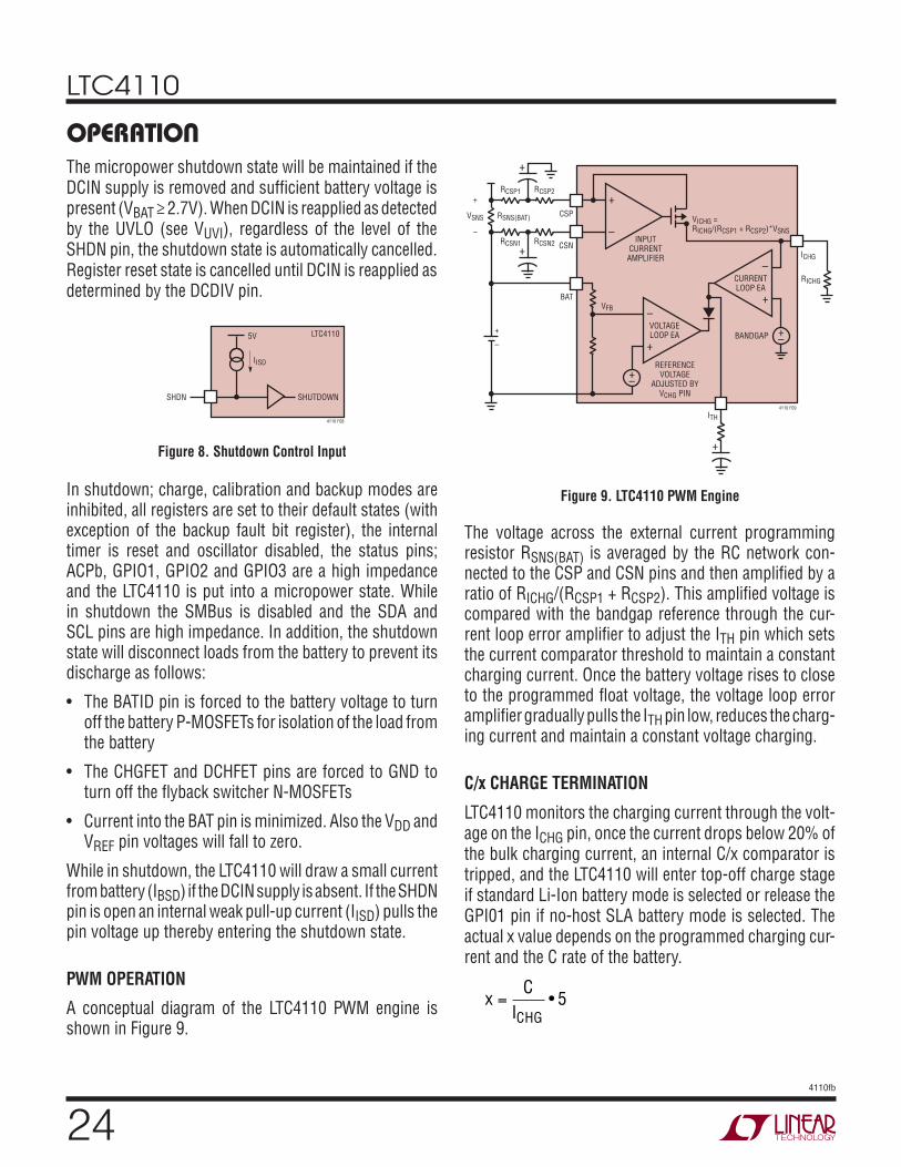
The voltage across the external current programming resistor RSNS(BAT) is averaged by the RC network con-nected to the CSP and CSN pins and then amplifi ed by a ratio of RICHG/(RCSP1 + RCSP2). This amplifi ed voltage is compared with the bandgap reference through the cur-rent loop error amplifi er to adjust the ITH pin which sets the current comparator threshold to maintain a constant charging current. Once the battery voltage rises to close to the programmed fl oat voltage, the voltage loop error amplifi er gradually pulls the ITH pin low, reduces the charg-ing current and maintain a constant voltage charging.
C/x CHARGE TERMINATION
LTC4110 monitors the charging current through the volt-age on the ICHG pin, once the current drops below 20% of the bulk charging current, an internal C/x comparator is tripped, and the LTC4110 will enter top-off charge stage if standard Li-Ion battery mode is selected or release the GPI01 pin if no-host SLA battery mode is selected. The actual x value depends on the programmed charging cur-rent and the C rate of the battery.
xC
ICHG= • 5
OPERATION
Figure 9. LTC4110 PWM EngineIn shutdown; charge, calibration and backup modes are inhibited, all registers are set to their default states (with exception of the backup fault bit register), the internal timer is reset and oscillator disabled, the status pins; ACPb, GPIO1, GPIO2 and GPIO3 are a high impedance and the LTC4110 is put into a micropower state. While in shutdown the SMBus is disabled and the SDA and SCL pins are high impedance. In addition, the shutdown state will disconnect loads from the battery to prevent its discharge as follows:
• The BATID pin is forced to the battery voltage to turn off the battery P-MOSFETs for isolation of the load from the battery
• The CHGFET and DCHFET pins are forced to GND to turn off the fl yback switcher N-MOSFETs
• Current into the BAT pin is minimized. Also the VDD and VREF pin voltages will fall to zero.
While in shutdown, the LTC4110 will draw a small current from battery (IBSD) if the DCIN supply is absent. If the SHDN pin is open an internal weak pull-up current (IISD) pulls the pin voltage up thereby entering the shutdown state.
PWM OPERATION
A conceptual diagram of the LTC4110 PWM engine is shown in Figure 9.
Figure 8. Shutdown Control Input
SHDN
LTC4110
SHUTDOWN
4110 F08
5V
IISD
VFB
4110 F09
BAT
RCSP2
CSP
RCSP1
RSNS(BAT)VSNS
+
– –
+
+
+
–
RCSN2 CSNINPUT
CURRENTAMPLIFIER
VICHG = RICHG/(RCSP1 + RCSP2)*VSNS
VOLTAGELOOP EA
REFERENCEVOLTAGE
ADJUSTED BYVCHG PIN
+
–CURRENTLOOP EA
BANDGAP
RCSN1
+
+
ITH
RICHG
ICHG
+–
+–
+
–
LTC4110
254110fb
Where:
C = C rate of the battery
ICHG = Programmed charging current
For Example, if we charge a 3Ah battery with 1A current, then x = 15.
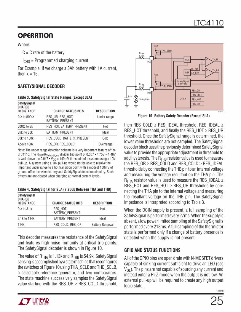
SAFETYSIGNAL DECODER
Table 3. SafetySignal State Ranges (Except SLA)
SafetySignal CHARGE RESISTANCE CHARGE STATUS BITS DESCRIPTION
0Ω to 500Ω RES_UR, RES_HOT,BATTERY_PRESENT
Under range
500Ω to 3k RES_HOT, BATTERY_PRESENT Hot
3kΩ to 30k BATTERY_PRESENT Ideal
30k to 100k RES_COLD, BATTERY_PRESENT Cold
Above 100k RES_OR, RES_COLD Overrange
Note: The under range detection scheme is a very important feature of the
LTC4110. The RTHA/RSafetySignal divider trip point of 0.307 • 4.75V = 1.46V
is well above the 0.047 • VDD = 140mV threshold of a system using a 10k
pull-up. A system using a 10k pull-up would not be able to resolve the
important under range to a hot transition point with a modest 100mV of
ground offset between battery and SafetySignal detection circuitry. Such
offsets are anticipated when charging at normal current levels.
Table 4. SafetySignal for SLA (7.256k Between THA and THB)
SafetySignal CHARGE RESISTANCE CHARGE STATUS BITS DESCRIPTION
0Ω to 3.1k RES_HOT,BATTERY_PRESENT
Hot
3.1k to 114k BATTERY_PRESENT Ideal
114k RES_COLD, RES_OR Battery Removal
This decoder measures the resistance of the SafetySignal and features high noise immunity at critical trip points. The SafetySignal decoder is shown in Figure 10.
The value of RTHA is 1.13k and RTHB is 54.9k. SafetySignal sensing is accomplished by a state machine that reconfi gures the switches of Figure 10 using THA_SELB and THB_SELB, a selectable reference generator, and two comparators. The state machine successively samples the SafetySignal value starting with the RES_OR ≥ RES_COLD threshold,
then RES_C0LD ≥ RES_IDEAL threshold, RES_IDEAL ≥ RES_HOT threshold, and fi nally the RES_HOT ≥ RES_UR threshold. Once the SafetySignal range is determined, the lower value thresholds are not sampled. The SafetySignal decoder block uses the previously determined SafetySignal value to provide the appropriate adjustment in threshold to add hysteresis. The RTHB resistor value is used to measure the RES_OR ≥ RES_COLD and RES_COLD ≥ RES_IDEAL thresholds by connecting the THB pin to an internal voltage and measuring the voltage resultant on the THA pin. The RTHA resistor value is used to measure the RES_IDEAL ≥ RES_HOT and RES_HOT ≥ RES_UR thresholds by con-necting the THA pin to the internal voltage and measuring the resultant voltage on the THB pin. The SafetySignal impedance is interpreted according to Table 3.
When the DCIN supply is present, a full sampling of the SafetySignal is performed every 27ms. When the supply is absent, a low power limited sampling of the SafetySignal is performed every 218ms. A full sampling of the thermistor state is performed only if a change of battery presence is detected when the supply is not present.
GPIO AND STATUS FUNCTIONS
All of the GPIO pins are open drain with N-MOSFET drivers capable of sinking current suffi cient to drive an LED (see VOL). The pins are not capable of sourcing any current and instead enter a Hi-Z mode when the output is not low. An external pull-up will be required to create any high output logic state.
OPERATION
Figure 10. Battery Safety Decoder (Except SLA)
VINT
SafetySignalCONTROL
RSafetySignal
CSSLATCH
RES_OR
TH_HIMUX
THB_SELB
4110 F10
+
–
TH_LOHI_REF
REF LO_REF
+
–
VINT
RTHB54.9k
THA_SELB
THB
RTHA1.13k
THA
RES_COLD
RES_HOT
RES_UR
LTC4110
264110fb
The three I/O outputs, GPIO1, GPIO2 and GPIO3 are digital I/O pins with two modes of operation.
1) General Purpose I/O
2) Status Reporting
A host can set the mode of each I/O pin with each I/O pin’s setting independent of the others such that any combination of status reporting or bit I/O can be implemented. Only a UVLO or a SHDN event will change the GPIO_n_EN bits back to default values. If you enable a GPIO pin to report status output, it overrides the GPIO_n_OUT setting. In addition, the LTC4110 supports a special power up mode of status reporting on all 3 IO pins for standalone applica-tions where it is assumed “no host” exists. This power up status mode is enabled if the SELA pin is set to 0.5 • VREF voltage as developed from VREF pin resistor divider. This mode does not actually disable the SMBus in any way and if a host does exist in this power up mode, the host can reprogram the I/O settings at any time.
All GPIO pins operate as digital inputs at all times regard-less of the pin settings with pin state reported on the GPIO_n_IN bits in the BBuStatus() register. However to actually read digital input data from an external device, you must disable the GPIO_n_EN bit. Otherwise the input will simply refl ect the output state assuming external powered pull-ups exist.
There are a total of 5 status signals possible. CHGb, C/xb, BKUP-FLTb, CHG_FLTb, and CAL_COMPLETEb. Each of these signals is asserted low on the output when they are true. CHGb is an asserted low signal when either CHG_STATE_0 or CHG_STATE_1 is set to one. C/xb is asserted low signal when C/x state in the charge cycle is reached. This status signal is only available if the TYPE pin is set to SLA mode and replaces the CHGb status output. BKUP_FLTb is asserted low when the BKUP_FLT bit is set to one in the BBuStatus() register. BKUP_FLT is a sticky bit that is designed to be cleared primarily through the setting of the BUFLT_RST bit in the BBuControl() register. The value of this bit does not inhibit charging or calibration functions. CHG_FLTb is asserted low when the CHG_FLT bit is set to one in the BBuStatus() register. CAL_COMPLETEb bit is asserted low when the conditions of successful calibra-tion cycle are met. CAL_COMPLETEb status output can be used as an interrupt to a host for the purpose of help implementing a simple gas gauge function or capacity verifi cation function with a standard battery. However, if the LTC4110 is set up in no host mode, CAL_COMPLETEb as a status signal is not considered usable since it is assumed there is no host to enable calibration mode. Therefore the CHG_FLTb signal is substituted for CAL_COMPLETEb as the status output signal. Table 5 describes the specifi c modes and status signal options of each GPIO pin.
OPERATION
Table 5b. GPIO1 Power Up Mode (SELA = 0.5 • VREF)
FORCED BIT SETTINGS TYPE = SLA GPIO_1 MODE DATA NOTE
GPIO_1_EN GPIO_1_OUT GPIO_1_CHG
1 X 1 0 Status Output CHGb With Pull-Up
1 X 1 1 Status Output C/xb With Pull-Up
Table 5a. GPIO1 Modes
HOST PROGRAMMED BIT SETTINGS GPIO_1 MODE DATA NOTE
GPIO_1_EN GPIO_1_OUT GPIO_1_CHG
0 0 0 Digital Input Input Data GPIO_1_IN
1 X 1 Status Output CHGb With Pull-Up
1 0 0 Digital Output 0 With Pull-Up
1 1 0 Digital Output 1 With Pull-Up
LTC4110
274110fb
OPERATION
SMBUS INTERFACE
All communications over the SMBus are interpreted by the SMBus interface block. The SMBus interface is a SMBus slave device. All internal LTC4110 registers may be updated and accessed through the SMBus interface as required. The SMBus protocol is a derivative of the I2C-BusTM. (For a complete description of the bus protocol requirements, reference “The I2C-Bus and How to Use It, V1.0” by Phil-ips®, and “System Management Bus Specifi cation, Version 1.1,” from the SMBus organization). See Table 6: Register
Command Set Description and Table 7: Summary of Sup-ported SMBus Functions, for complete details.
All data is clocked into the shift register on the rising edge of SCL. All data is clocked out of the shift register on the falling edge of SCL. Detection of an SMBus Stop condi-tion, or power-on reset will reset the SMBus interface to an initial state at any time. The LTC4110 command set is interpreted by the SMBus interface and passed onto the charger controller block as control signals or updates to internal registers. Smart battery charge commands are
Table 5c. GPIO2 Modes
HOST PROGRAMMED BIT SETTINGS GPIO_2 MODE DATA NOTE
GPIO_2_EN GPIO_2_OUT GPIO_2_BUFLT
0 0 0 Digital Input Input Data GPIO_2_IN
1 X 1 Status Output BKUP_FLTb With Pull-Up
1 0 0 Digital Output 0 With Pull-Up
1 1 0 Digital Output 1 With Pull-Up
Table 5d. GPIO2 Power Up Mode (SELA = 0.5 • VREF)
FORCED BIT SETTINGS GPIO_2 MODE DATA NOTE
GPIO_2_EN GPIO_2_OUT GPIO_2_ BUFLT
1 X 1 Status Output BKUP_FLTb With Pull-Up
Table 5e. GPIO3 Modes
HOST PROGRAMMED BIT SETTINGS GPIO_3 MODE DATA NOTE
GPIO_3_EN GPIO_3_OUT GPIO_3_CAL
0 0 0 Digital Input Input Data GPIO_3_IN
1 X 1 Status Output CAL_COMPLETEb With Pull-Up
1 0 0 Digital Output 0 With Pull-Up
1 1 0 Digital Output 1 With Pull-Up
Table 5f. GPIO3 Power Up Mode (SELA = 0.5 • VREF)
FORCED BIT SETTINGS GPIO_3 MODE DATA NOTE
GPIO_3_EN GPIO_3_OUT GPIO_3_ CAL
1 X 1 Status Output CHG_FLTb With Pull-Up
LTC4110
284110fb
OPERATIONprocessed to allow compliance with smart battery charge and discharge termination and protection control. How-ever, there is no actual value processing of the voltage or current charge commands. IC will acknowledge all smart battery write commands, but process only a subset of them. Full SMBus error and reset handling is supported. The SMBus remains functional during backup mode, but not in SHDN mode.
The LTC4110 SMBus address can be changed when standard batteries are used to facilitate redundant backup systems. Connect SELA pin to GND for 12h, VDD for 28h and VREF for 20h. When a smart battery is selected by the TYPE pin the SELA pin must be connected to GND to select address 12h. Note: Although there are only 7 address bits for SMBus, the above addresses shown follow the smart battery convention of including the Read/Write bit as part of the address value. The Read/Write bit becomes the LSB of the SMBus address with the Read/Write bit value assumed to be a 0 value.
If multiple LTC4110s with smart batteries are to be used, each LTC4110 must be SMBus isolated from all other LTC4110s so the main bus or host bus can only see one LTC4110 and its corresponding smart battery at a time. Failure to do so will cause multiple LTC4110s and smart batteries responding to a single host query resulting in errors. There are multiple channel SMBus multiplexer ICs such as the LTC4305 and LTC4306 to help implement the required isolation. Furthermore, if a given SMBus is high in SMBus device count or long in length, you may want to consider using SMBus accelerators. The above ICs listed support that option.
If the SMBus is not used or to force all GPIOs to status mode upon power-up, connect SELA to a typically 0.5 • VREF voltage from VREF pin resistor divider. The SMBus address then, if used, will be 12h.
Pull-ups are required on the SDA and SCL pin such that when they are not being used, they are in a default high state that means no bus activity. The pull-up voltage need only be high enough to satisfy the logic high threshold. Tying the pins low is a valid state on the SMBus that means anything but the bus is free. This state will force the LTC4110’s internal SMBus state machine to reset itself because it thinks the SMBus is hung.
The LTC4110 does not support or respond to the following SMBus V1.1 timing specifi cations:
a) TTIMEOUT (This is not to be confused with the LTC4110’s tTIMEOUT specifi cation.)
b) TLOW:SEXT
c) TLOW:MEXT
The above specifi cations have to do with detecting bus hangs or SMBus devices that are taking too long to reply using clock stretching and slowing down the SMBus bandwidth. The LTC4110 is a slave only device that does not do any clock stretching and works all the way up to maximum 100kHz bus speed. It will not hang the bus. The design will always reset its SMBus interface upon receiving an SMBus Start Bit or a Stop Bit regardless of the prior state of the bus.
LTC4110
294110fb
OPERATION
LABEL DESCRIPTION
ChargerStatus() – Read Only. The SMBus host uses this command to read the LTC4110’s charge status bits.
AC_PRESENT Set to 1 when suffi cient input voltage (DCDIV > VAC + VACH and DCIN above UVLO) available and switches load from battery to main supply. Zero indicates backup mode engaged.
BATTERY_PRESENT BATTERY_PRESENT is set if a battery is present, otherwise it is cleared. The LTC4110 uses the SafetySignal to determine battery presence. If the LTC4110 detects a RES_OR condition, the BATTERY_PRESENT bit is cleared immediately. The LTC4110 will not set the BATTERY_PRESENT bit until it successfully samples the SafetySignal twice and does not detect a RES_OR condition on either sampling. If AC is not present (DCDIV < VAC or DCIN below UVLO), this bit may not be set for up to one-half second after the battery is connected to the SafetySignal. The ChargingCurrent() and ChargingVoltage() register values are immediately cleared whenever this bit is cleared. Charging will never be allowed if this bit is cleared.
ALARM_INHIBITED ALARM_INHIBITED bit is set if a valid AlarmWarning() message has been received and charging is inhibited as a result. This bit is cleared if POR_RESET is set, both ChargingVoltage() and ChargingCurrent() are rewritten to the LTC4110, the power is removed (DCDIV < VAC or DCIN below UVLO), the SHDN pin is set high, or if a battery is removed.
RES_UR Set to 1 when NTC pin is below 500Ω typical. This bit is never set when TYPE pin selects SLA battery..
RES_HOT The RES_HOT bit is set only when the SafetySignal resistance is less than 3kΩ (3.1kΩ for SLA) typical, which indicates a hot battery. The RES_HOT bit will be set whenever the RES_UR bit is set.
RES_COLD The RES_COLD bit is set only when the SafetySignal resistance value is greater than 30kΩ typical. The SafetySignal indicates a cold battery. The RES_COLD bit will be set whenever the RES_OR bit is set. This bit is the same as RES_OR for SLA.
RES_OR The RES_OR bit is set when the SafetySignal resistance value is above 100kΩ (114kΩ for SLA) typical. The SafetySiganl indicates an open circuit.
LEVEL:3/LEVEL:2 The LTC4110 always reports itself as a Level 2 Smart Battery Charger.
CHARGE_INHIBITED Indicates charge inhibited is enabled when set to a one. This is a duplicate of the CHARGE_INHIBIT bit in the BBuStatus() register.
ChargingCurrent() – Write Only. The battery, system host or other master device sends the desired charging current to the LTC4110.
ChargingCurrent() LTC4110 only monitors for zero or non-zero values. A value of zero will stop the charger. A non-zero value here, and for ChargingVoltage(), will restart the charger.
ChargingVoltage() – Write Only. The Battery, System Host or other master device sends the desired charging voltage to the LTC4110.
ChargingVoltage() LTC4110 only monitors for zero or non-zero values. A value of zero will stop the charger. A non-zero value here, and for ChargingCurrent(), will restart the charger.
AlarmWarning() – Write Only. The Smart Battery, acting as a bus master device, sends the AlarmWarning() message to the LTC4110 to notify it that one or more alarm conditions exist. Alarm indications are encoded as bit fi elds in the battery’s status register, which is then sent to the LTC4110 by this function. Only the OVER_CHARGED_ALARM, TERMINATE_CHARGE_ALARM,RESERVED_ALARM, OVER_TEMP_ALARM and TERMINATE_DISCHARGE_ALARM bits are supported by the LTC4110. The ALARM_INHIBITED bit in the ChargerStatus() register indicates whether a charging process or a calibration process was halted by a write to this register.
OVER_CHARGED_ALARM Set to one indicates battery has been overcharged and stops charge. Setting this bit will only stop a charging process (default = zero).
TERMINATE_CHARGE_ALARM Set to one indicates battery requesting charge termination. Setting this bit will only stop a charging process (default = zero).
RESERVED_ALARM Set to one for reserved alarm condition. Setting this bit will stop both a calibration process and a charging process (default = zero).
Table 6. Register Command Set Descriptions (XxxxXxxx() – Register Byte, XXXXXXXX – Status Bit)
LTC4110
304110fb
OPERATIONLABEL DESCRIPTION
OVER_TEMP_ALARM Set to one indicates battery is temperature is out of range. Setting this bit will stop both a calibration process and a charging process (default = zero).
TERMINATE_DISCHARGE_ALARM Set to one indicates battery requesting discharge termination. Smart battery only. Setting this bit will only stop a calibration process (default = zero).
BBuStatus() – Read Only. The SMBus host uses this command to read the LTC4110’s status bits.
CAL_ON Set to one indicates calibration in progress to discharge the battery.
CAL_COMPLETE Set to one indicates calibration process is complete. Can be used as a battery capacity indicator. Bit is cleared by CAL_RESET. This bit is available as a status signal output on the GPIO3 pin.
BKUP_ON Set to one verifi es backup mode is active
GPIO_1_IN Shows logic state of general purpose I/O Pin #1. This is always enabled.
GPIO_2_IN Shows logic state of general purpose I/O Pin #2. This is always enabled.
GPIO_3_IN Shows logic state of general purpose I/O Pin #3. This is always enabled.
CHG_FLT Set to one indicates battery charge fault.
BKUP_FLT Set to one indicates battery cell voltage < VDIS. This bit state is retained as long as suffi cient VBAT is applied. This bit is available as a status signal output on the GPIO2 port. This bit remains until either the SHDN pin is cycled or register bits POR_RESET or BUFLT_RST are set when DCOUT returns.
CAL_FLT Set to one indicates a calibration fault. Calibration terminated early.
CHG_STATE_0 Combined with CHG_STATE_1 indicates phase of charging. 00 = Off, 01 = precharge, 10 = bulk charge, 11 = top off charge
CHG_STATE_1 See CHG_STATE_0
CHARGE_INHIBITED Indicates charge inhibited is enabled when set to a one. This as a duplicate of CHARGE_INHIBIT bit in the ChargerStatus() register.
BBuControl() – Write Only. The SMBus host uses this command to control the LTC4110.
CAL_START Set to one starts a discharge based calibration of battery (default = self cleared to zero-off)
CAL_RESET Set to one clears the CAL_FLT as well as the CAL COMPLETE and CAL_ON status bits. If calibration is in progress, it will also stop the calibration process (default = self cleared to zero-off)
GPIO_1_EN Set to one enables GPIO1 pin as an output (default = set to one if programming SMBus not used by connecting SELA pin to 0.5VREF, otherwise default = set to zero/GPIO1 high-Z )
GPIO_2_EN Set to one enables GPIO2 pin as an output (default = set to one if programming SMBus not used by connecting SELA pin to 0.5VREF, otherwise default = set to zero/ GPIO2 high-Z)
GPIO_3_EN Set to one enables GPIO3 pin as an output (default = set to one if programming SMBus not used by connecting SELA pin to 0.5VREF, otherwise default = set to zero/ GPIO3 high-Z)
GPIO_1_OUT Programmable logic bit whose state will be refl ected on the GPIO1 pin if the GPIO_1_CHG bit is cleared (default = set to zero/GPIO1 pulled low)
GPIO_2_OUT Programmable logic bit whose state will be refl ected on the GPIO2 pin if the GPIO_2_BUFLT bit is cleared (default = set to zero/GPIO2 pulled low).
GPIO_3_OUT Programmable logic bit whose state will be refl ected on the GPIO3 pin if the GPIO_3_CALCOM bit is cleared (default = set to zero/GPIO3 pulled low)
LTC4110
314110fb
OPERATIONLABEL DESCRIPTION
GPIO_1_CHG Set to one sends an inverted CHG_ON (internal register, set to 1 when either CHG_STATE_0 or CHG_STATE_1 is set to 1) status signal out to the GPIO1 pin. If this bit is set, the value of CHG_ON overrides the value of the GPIO_1_OUT bit state. Pin must be output enabled with GPIO_1_EN bit (default = set to zero/off)
GPIO_2_BUFLT Set to one sends an inverted BKUP_FLT status signal out to the GPIO2 pin. If this bit is set, the value of BKUP_FLT overrides the value of the GPIO_2_OUT bit state. Pin must be output enabled with GPIO_2_EN bit (default = set to zero/off)
GPIO_3_CALCOM Set to one sends an inverted CAL_COMPLETE signal out to the GPIO3 pin. If this bit is set, the value of CAL_COMPLETE overrides the value of the GPIO_3_OUT bit state. Pin must be output enabled with GPIO_3_EN bit (default = set to zero/off)
RESET_TO_ZERO Set to one resets all faults and timers in charge and forces the ChargingCurrent() and ChargingVoltage() to zero values. Clears Alarm_Warning() register. Does not affect BBuControl() register. Bit clears to zero automatically after the command is executed (default = cleared to zero-no reset)
POR_RESET Resets LTC4110 to power-on default values. Setting the bit to a one will activate POR_RESET. POR_RESET performs a total chip wide reset like the SHDN pin function without the chip actually shutting down. This includes clearing any bits in registers. The bit clears itself automatically after the command is executed (default = cleared/no reset)
BUFLT_RST Resets the BKUP_FLT bit. The bit clears itself automatically after the command is executed (default = cleared).
CHARGE_INHIBIT Disables charging of battery. Set to one halts charge current while holding the charger state and pausing all battery charge timers without changing the ChargingCurrent() and ChargingVoltage() values. Charge may be enabled by clearing this bit. This bit is automatically cleared when power is reapplied or when a battery is re-inserted (default = cleared to zero-off)
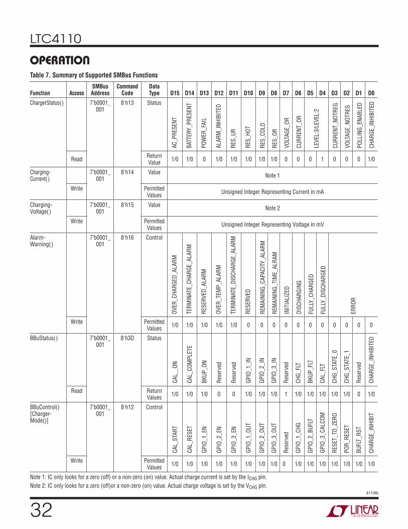
LTC4110
324110fb
Table 7. Summary of Supported SMBus Functions
OPERATION
Function AccessSMBusAddress
CommandCode
DataType D15 D14 D13 D12 D11 D10 D9 D8 D7 D6 D5 D4 D3 D2 D1 D0
ChargerStatus( ) 7’b0001_001
8'h13 Status
AC
_PR
ESEN
T
BAT
TER
Y_P
RES
ENT
PO
WER
_FA
IL
ALA
RM
_IN
HIB
ITED
RES
_UR
RES
_HO
T
RES
_CO
LD
RES
_OR
VO
LTA
GE_
OR
CU
RR
ENT_
OR
LEV
EL:3
/LEV
EL:2
CU
RR
ENT_
NO
TREG
VO
LTA
GE_
NO
TRES
PO
LLIN
G_E
NA
BLE
D
CH
AR
GE_
INH
IBIT
ED
ReadReturn Value
1/0 1/0 0 1/0 1/0 1/0 1/0 1/0 0 0 0 1 0 0 0 1/0
Charging-Current( )
7’b0001_001
8'h14 ValueNote 1
Write Permitted Values
Unsigned Integer Representing Current in mA
Charging-Voltage( )
7’b0001_001
8'h15 ValueNote 2
Write Permitted Values
Unsigned Integer Representing Voltage in mV
Alarm-Warning( )
7’b0001_001
8'h16 Control
OV
ER_C
HA
RG
ED_A
LAR
M
TER
MIN
ATE_
CH
AR
GE_
ALA
RM
RES
ERV
ED_A
LAR
M
OV
ER_T
EMP
_ALA
RM
TER
MIN
ATE_
DIS
CH
AR
GE_
ALA
RM
RES
ERV
ED
REM
AIN
ING
_CA
PA
CIT
Y_A
LAR
M
REM
AIN
ING
_TIM
E_A
LRA
M
INIT
IALI
ZED
DIS
CH
AR
GIN
G
FULL
Y_C
HA
RG
ED
FULL
Y_D
ISC
HA
RG
ED
ERR
OR
Write Permitted Values
1/0 1/0 1/0 1/0 1/0 0 0 0 0 0 0 0 0 0 0 0
BBuStatus( ) 7’b0001_001
8'h3D Status
CA
L__O
N
CA
L_C
OM
PLE
TE
BK
UP
_ON
Res
erve
d
Res
erve
d
GP
IO_1
_IN
GP
IO_2
_IN
GP
IO_3
_IN
Res
erve
d
CH
G_F
LT
BK
UP
_FLT
CA
L_FL
T
CH
G_S
TATE
_0
CH
G_S
TATE
_1
Res
erve
d
CH
AR
GE_
INH
IBIT
ED
Read ReturnValues
1/0 1/0 1/0 0 0 1/0 1/0 1/0 1 1/0 1/0 1/0 1/0 1/0 0 1/0
BBuControl()[Charger-Mode()]
7’b0001_001
8'h12 Control
CA
L_S
TAR
T
CA
L_R
ESET
GP
IO_1
_EN
GP
IO_2
_EN
GP
IO_3
_EN
GP
IO_1
_OU
T
GP
IO_2
_OU
T
GP
IO_3
_OU
T
Res
erve
d
GP
IO_1
_CH
G
GP
IO_2
_BU
FLT
GP
IO_3
_CA
LCO
M
RES
ET_T
O_Z
ERO
PO
R_R
ESET
BU
FLT_
RS
T
CH
AR
GE_
INH
IBIT
Write Permitted Values
1/0 1/0 1/0 1/0 1/0 1/0 1/0 1/0 0 1/0 1/0 1/0 1/0 1/0 1/0 1/0
Note 1: IC only looks for a zero (off) or a non-zero (on) value. Actual charge current is set by the ICHG pin.
Note 2: IC only looks for a zero (off)or a non-zero (on) value. Actual charge voltage is set by the VCHG pin.
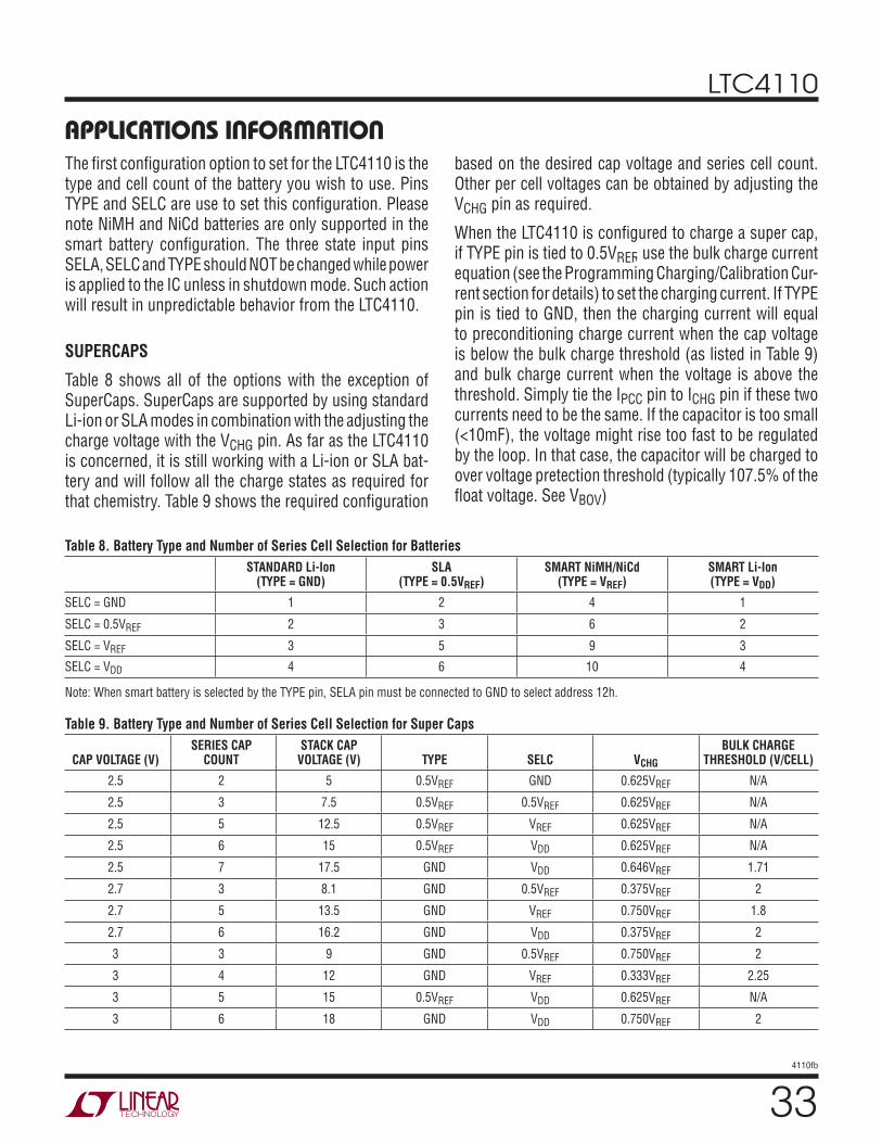
LTC4110
334110fb
based on the desired cap voltage and series cell count. Other per cell voltages can be obtained by adjusting the VCHG pin as required.
When the LTC4110 is confi gured to charge a super cap, if TYPE pin is tied to 0.5VREF, use the bulk charge current equation (see the Programming Charging/Calibration Cur-rent section for details) to set the charging current. If TYPE pin is tied to GND, then the charging current will equal to preconditioning charge current when the cap voltage is below the bulk charge threshold (as listed in Table 9) and bulk charge current when the voltage is above the threshold. Simply tie the IPCC pin to ICHG pin if these two currents need to be the same. If the capacitor is too small (<10mF), the voltage might rise too fast to be regulated by the loop. In that case, the capacitor will be charged to over voltage pretection threshold (typically 107.5% of the fl oat voltage. See VBOV)
The fi rst confi guration option to set for the LTC4110 is the type and cell count of the battery you wish to use. Pins TYPE and SELC are use to set this confi guration. Please note NiMH and NiCd batteries are only supported in the smart battery confi guration. The three state input pins SELA, SELC and TYPE should NOT be changed while power is applied to the IC unless in shutdown mode. Such action will result in unpredictable behavior from the LTC4110.
SUPERCAPS
Table 8 shows all of the options with the exception of SuperCaps. SuperCaps are supported by using standard Li-ion or SLA modes in combination with the adjusting the charge voltage with the VCHG pin. As far as the LTC4110 is concerned, it is still working with a Li-ion or SLA bat-tery and will follow all the charge states as required for that chemistry. Table 9 shows the required confi guration
APPLICATIONS INFORMATION
Table 8. Battery Type and Number of Series Cell Selection for Batteries
STANDARD Li-Ion(TYPE = GND)
SLA(TYPE = 0.5VREF)
SMART NiMH/NiCd(TYPE = VREF)
SMART Li-Ion(TYPE = VDD)
SELC = GND 1 2 4 1
SELC = 0.5VREF 2 3 6 2
SELC = VREF 3 5 9 3
SELC = VDD 4 6 10 4
Note: When smart battery is selected by the TYPE pin, SELA pin must be connected to GND to select address 12h.
Table 9. Battery Type and Number of Series Cell Selection for Super Caps
CAP VOLTAGE (V)SERIES CAP
COUNTSTACK CAP
VOLTAGE (V) TYPE SELC VCHG
BULK CHARGE THRESHOLD (V/CELL)
2.5 2 5 0.5VREF GND 0.625VREF N/A
2.5 3 7.5 0.5VREF 0.5VREF 0.625VREF N/A
2.5 5 12.5 0.5VREF VREF 0.625VREF N/A
2.5 6 15 0.5VREF VDD 0.625VREF N/A
2.5 7 17.5 GND VDD 0.646VREF 1.71
2.7 3 8.1 GND 0.5VREF 0.375VREF 2
2.7 5 13.5 GND VREF 0.750VREF 1.8
2.7 6 16.2 GND VDD 0.375VREF 2
3 3 9 GND 0.5VREF 0.750VREF 2
3 4 12 GND VREF 0.333VREF 2.25
3 5 15 0.5VREF VDD 0.625VREF N/A
3 6 18 GND VDD 0.750VREF 2
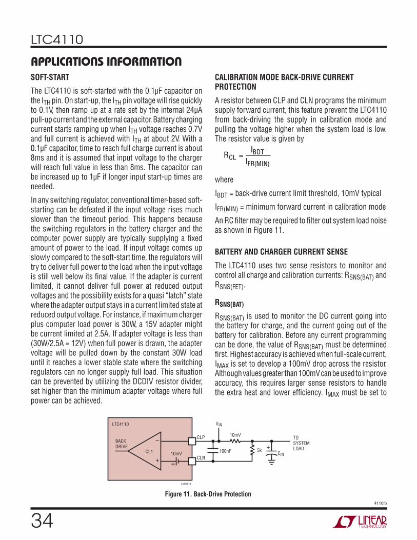
LTC4110
344110fb
SOFT-START
The LTC4110 is soft-started with the 0.1μF capacitor on the ITH pin. On start-up, the ITH pin voltage will rise quickly to 0.1V, then ramp up at a rate set by the internal 24μA pull-up current and the external capacitor. Battery charging current starts ramping up when ITH voltage reaches 0.7V and full current is achieved with ITH at about 2V. With a 0.1μF capacitor, time to reach full charge current is about 8ms and it is assumed that input voltage to the charger will reach full value in less than 8ms. The capacitor can be increased up to 1μF if longer input start-up times are needed.
In any switching regulator, conventional timer-based soft-starting can be defeated if the input voltage rises much slower than the timeout period. This happens because the switching regulators in the battery charger and the computer power supply are typically supplying a fi xed amount of power to the load. If input voltage comes up slowly compared to the soft-start time, the regulators will try to deliver full power to the load when the input voltage is still well below its fi nal value. If the adapter is current limited, it cannot deliver full power at reduced output voltages and the possibility exists for a quasi “latch” state where the adapter output stays in a current limited state at reduced output voltage. For instance, if maximum charger plus computer load power is 30W, a 15V adapter might be current limited at 2.5A. If adapter voltage is less than (30W/2.5A = 12V) when full power is drawn, the adapter voltage will be pulled down by the constant 30W load until it reaches a lower stable state where the switching regulators can no longer supply full load. This situation can be prevented by utilizing the DCDIV resistor divider, set higher than the minimum adapter voltage where full power can be achieved.
APPLICATIONS INFORMATIONCALIBRATION MODE BACK-DRIVE CURRENT PROTECTION
A resistor between CLP and CLN programs the minimum supply forward current, this feature prevent the LTC4110 from back-driving the supply in calibration mode and pulling the voltage higher when the system load is low. The resistor value is given by
RI
ICLBDT
FR MIN=
( )
where
IBDT = back-drive current limit threshold, 10mV typical
IFR(MIN) = minimum forward current in calibration mode
An RC fi lter may be required to fi lter out system load noise as shown in Figure 11.
BATTERY AND CHARGER CURRENT SENSE
The LTC4110 uses two sense resistors to monitor and control all charge and calibration currents: RSNS(BAT) and RSNS(FET).
RSNS(BAT)
RSNS(BAT) is used to monitor the DC current going into the battery for charge, and the current going out of the battery for calibration. Before any current programming can be done, the value of RSNS(BAT) must be determined fi rst. Highest accuracy is achieved when full-scale current, IMAX is set to develop a 100mV drop across the resistor. Although values greater than 100mV can be used to improve accuracy, this requires larger sense resistors to handle the extra heat and lower effi ciency. IMAX must be set to
Figure 11. Back-Drive Protection
10mVTOSYSTEMLOAD
4110 F11
–
+
VIN
CIN100nF
10mV5k
CLP
CLN
CL1
LTC4110
BACKDRIVE +
+
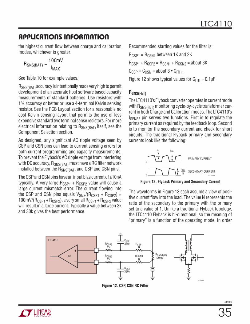
LTC4110
354110fb
APPLICATIONS INFORMATIONthe highest current fl ow between charge and calibration modes, whichever is greater.
RmV
ISNS BATMAX
( ) =100
See Table 10 for example values.
RSNS(BAT) accuracy is intentionally made very high to permit development of an accurate host software based capacity measurements of standard batteries. Use resistors with 1% accuracy or better or use a 4-terminal Kelvin sensing resistor. See the PCB Layout section for a reasonable no cost Kelvin sensing layout that permits the use of less expensive standard two terminal sense resistors. For more electrical information relating to RSNS(BAT) itself, see the Component Selection section.
As designed, any signifi cant AC ripple voltage seen by CSP and CSN pins can lead to current sensing errors for both current programming and capacity measurements. To prevent the Flyback’s AC ripple voltage from interfering with DC accuracy, RSNS(BAT) must have a RC fi lter network installed between the RSNS(BAT) and CSP and CSN pins.
The CSP and CSN pins have an input bias current of ±10nA typically. A very large RCSP1 + RCSP2 value will cause a large current mismatch error. The current fl owing into the CSP and CSN pins equals VSNS/(RCSP1 + RCSP2) = 100mV/(RCSP1 + RCSP2), a very small RCSP1 + RCSP2 value will result in a large current. Typically a value between 3k and 30k gives the best performance.
Figure 12. CSP, CSN RC Filter
CCSP330n
CCSN330n
RSNS(BAT)100mV
RCSP22k
RCSN22k
RCSP11k
RCSN1
1k
4110 F12
–
+
LTC4110
CA
Recommended starting values for the fi lter is:
RCSP1 = RCSN1 between 1K and 2K
RCSP1 + RCSP2 = RCSN1 + RCSN2 = about 3K
CCSP = CCSN = about 3 • CITH.
Figure 12 shows typical values for CITH = 0.1μF
RSNS(FET)
The LTC4110’s Flyback converter operates in current mode with RSNS(FET) monitoring cycle-by-cycle transformer cur-rent in both Charge and Calibration modes. The LTC4110’s ISENSE pin serves two functions. First is to regulate the primary current as required by the feedback loop. Second is to monitor the secondary current and check for short circuits. The traditional Flyback primary and secondary currents look like the following:
Figure 13. Flyback Primary and Secondary Current
ΔI IPRI
SECONDARY CURRENT
PRIMARY CURRENT
IPRI
N
0
0 4110 F13
The waveforms in Figure 13 each assume a view of posi-tive current fl ow into the load. The value N represents the ratio of the secondary to the primary with the primary set to a value of 1. Unlike a traditional Flyback topology, the LTC4110 Flyback is bi-directional, so the meaning of “primary” is a function of the operating mode. In order
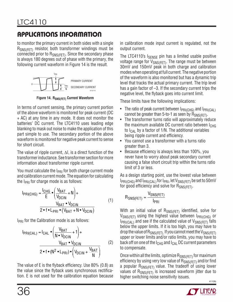
LTC4110
364110fb
to monitor the primary current in both sides with a single RSNS(FET) resistor, both transformer windings must be connected prior to RSNS(FET). Since the secondary phase is always 180 degrees out of phase with the primary, the following current waveform in Figure 14 is the result.
APPLICATIONS INFORMATION
IPRI
SECONDARY CURRENT
PRIMARY CURRENT
IPRI
N
0
4110 F14
Figure 14. RSNS(FET) Current Waveform
in calibration mode input current is regulated, not the output current.
The LTC4110’s ISENSE pin has a limited usable positive voltage range for VSNS(FET). The range must be between 30mV and 150mV peak in both charge and calibration modes when operating at full current. The negative portion of the waveform is also monitored but has a dynamic trip level that tracks the actual primary current. The trip level has a gain factor of –3. If the secondary current trips the negative level, the fl yback goes into current limit.
These limits have the following implications:
• The ratio of peak current between IPRI(CHG) and IPRI(CAL) cannot be greater than 5-to-1 as seen by RSNS(FET).
• The transformer turns ratio will approximately reduce the maximum available DC current ratio between ICHG to ICAL by a factor of 1/N. The additional variables being ripple current and effi ciency.
• You cannot use a transformer with a turns ratio greater than 3.
• Because effi ciency is always less than 100%, you never have to worry about peak secondary current causing a false short circuit trip within the turns ratio limit of 3 or less.
As a design starting point, use the lowest value between IPRI(CHG) and IPRI(CAL) for IPRI, let VSNS(FET) be set to 50mV for good effi ciency and solve for RSNS(FET).
RV
ISNS FETSNS FET
PRI( )
( )=
With an initial value of RSNS(FET) identifi ed, solve for VSNS(FET) using the highest value between IPRI(CHG) or IPRI(CAL) and see if the calculated value of VSNS(FET) falls below the upper limits. If it is too high, you may have to drop the value of RSNS(FET). If you cannot meet the VSNS(FET)
upper or lower limits and/or ratio limits, you may have to back off on one of the ICHG and ICAL DC current parameters to compensate.
Once within all the limits, optimize RSNS(FET) for maximum effi ciency by using very low value of RSNS(FET) and/or fi nd a popular RSNS(FET) value. The tradeoff of using lower values of RSNS(FET) is increased waveform jitter due to higher switching noise sensitivity issues.
In terms of current sensing, the primary current portion of the above waveform is monitored for peak current (DC + AC) at any time in any mode. It does not monitor the batteries’ DC current. The LTC4110 uses leading edge blanking to mask out noise to make the application of this part simple to use. The secondary portion of the above waveform is monitored for negative peak current to sense for short circuit.
The value of ripple current, ΔI, is a direct function of the transformer inductance. See transformer section for more information about transformer ripple current.
You must calculate the IPRI for both charge current mode and calibration current mode. The equation for calculating the IPRI for charge mode is as follows:
IPRI(CHG) =ICHG
E• VBAT
VDCIN+N +
VBAT • VDCIN2 • f • LPRI • VBAT +N • VDCIN( )
(1)
IPRI for the Calibration mode is as follows:
IPRI(CAL) = ICAL • VBATN • VDCIN
+1 +
VBAT • VDCIN
2 • f • (N2 • LPRI) • VDCIN +VBAT
N
(2)
The value of E is the fl yback effi ciency. Use 80% (0.8) as the value since the fl yback uses synchronous rectifi ca-tion. E is not used for the calibration equation because
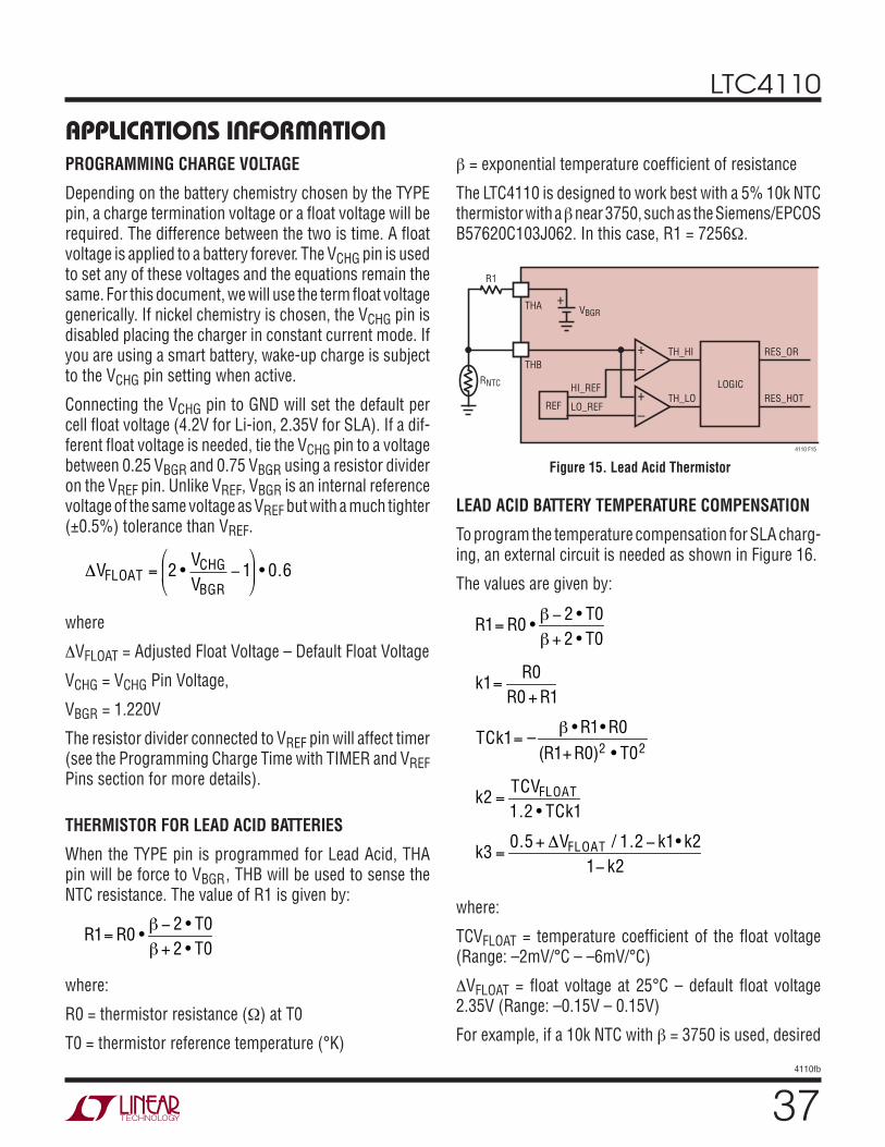
LTC4110
374110fb
PROGRAMMING CHARGE VOLTAGE
Depending on the battery chemistry chosen by the TYPE pin, a charge termination voltage or a fl oat voltage will be required. The difference between the two is time. A fl oat voltage is applied to a battery forever. The VCHG pin is used to set any of these voltages and the equations remain the same. For this document, we will use the term fl oat voltage generically. If nickel chemistry is chosen, the VCHG pin is disabled placing the charger in constant current mode. If you are using a smart battery, wake-up charge is subject to the VCHG pin setting when active.
Connecting the VCHG pin to GND will set the default per cell fl oat voltage (4.2V for Li-ion, 2.35V for SLA). If a dif-ferent fl oat voltage is needed, tie the VCHG pin to a voltage between 0.25 VBGR and 0.75 VBGR using a resistor divider on the VREF pin. Unlike VREF, VBGR is an internal reference voltage of the same voltage as VREF but with a much tighter (±0.5%) tolerance than VREF.
VFLOAT = 2 • VCHGVBGR
1 • 0.6
where
ΔVFLOAT = Adjusted Float Voltage – Default Float Voltage
VCHG = VCHG Pin Voltage,
VBGR = 1.220V
The resistor divider connected to VREF pin will affect timer (see the Programming Charge Time with TIMER and VREF Pins section for more details).
THERMISTOR FOR LEAD ACID BATTERIES
When the TYPE pin is programmed for Lead Acid, THA pin will be force to VBGR, THB will be used to sense the NTC resistance. The value of R1 is given by:
R1= R0 • β− 2 • T0
β+ 2 • T0
where:
R0 = thermistor resistance (Ω) at T0
T0 = thermistor reference temperature (°K)
β = exponential temperature coeffi cient of resistance
The LTC4110 is designed to work best with a 5% 10k NTC thermistor with a β near 3750, such as the Siemens/EPCOS B57620C103J062. In this case, R1 = 7256Ω.
APPLICATIONS INFORMATION
Figure 15. Lead Acid Thermistor
RNTC
TH_HI
VBGR
+
–
TH_LO
RES_OR
RES_HOTHI_REF
REF LO_REF+
–
THB
R1
THA
LOGIC
+
4110 F15
LEAD ACID BATTERY TEMPERATURE COMPENSATION
To program the temperature compensation for SLA charg-ing, an external circuit is needed as shown in Figure 16.
The values are given by:
R1= R0 • β− 2 • T0β+ 2 • T0
k1=R0
R0 +R1
TCk1= – β • R1• R0(R1+R0)2 • T02
k2 =TCVFLOAT
1.2 • TCk1
k3 =0.5+ΔVFLOAT / 1.2− k1• k2
1− k2
where:
TCVFLOAT = temperature coeffi cient of the fl oat voltage (Range: –2mV/°C – –6mV/°C)
ΔVFLOAT = fl oat voltage at 25°C – default fl oat voltage 2.35V (Range: –0.15V – 0.15V)
For example, if a 10k NTC with β = 3750 is used, desired
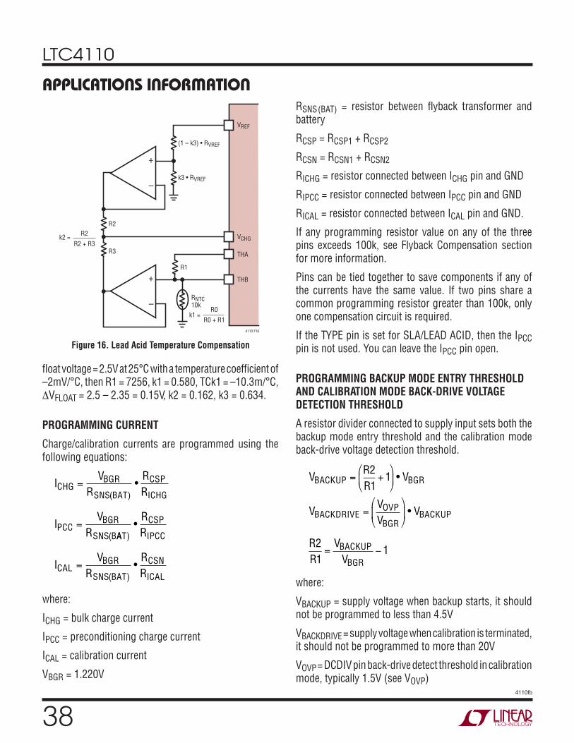
LTC4110
384110fb
RSNS(BAT) = resistor between fl yback transformer and battery
RCSP = RCSP1 + RCSP2
RCSN = RCSN1 + RCSN2
RICHG = resistor connected between ICHG pin and GND
RIPCC = resistor connected between IPCC pin and GND
RICAL = resistor connected between ICAL pin and GND.
If any programming resistor value on any of the three pins exceeds 100k, see Flyback Compensation section for more information.
Pins can be tied together to save components if any of the currents have the same value. If two pins share a common programming resistor greater than 100k, only one compensation circuit is required.
If the TYPE pin is set for SLA/LEAD ACID, then the IPCC pin is not used. You can leave the IPCC pin open.
PROGRAMMING BACKUP MODE ENTRY THRESHOLD AND CALIBRATION MODE BACK-DRIVE VOLTAGE DETECTION THRESHOLD
A resistor divider connected to supply input sets both the backup mode entry threshold and the calibration mode back-drive voltage detection threshold.
VBACKUP =R2R1
+1 • VBGR
VBACKDRIVE =VOVPVBGR
• VBACKUP
R2R1
=VBACKUP
VBGR1
where:
VBACKUP = supply voltage when backup starts, it should not be programmed to less than 4.5V
VBACKDRIVE = supply voltage when calibration is terminated, it should not be programmed to more than 20V
VOVP = DCDIV pin back-drive detect threshold in calibration mode, typically 1.5V (see VOVP)
fl oat voltage = 2.5V at 25°C with a temperature coeffi cient of –2mV/°C, then R1 = 7256, k1 = 0.580, TCk1 = –10.3m/°C, ΔVFLOAT = 2.5 – 2.35 = 0.15V, k2 = 0.162, k3 = 0.634.
PROGRAMMING CURRENT
Charge/calibration currents are programmed using the following equations:
IV
RRR
IV
R
CHGBGR
SNS BAT
CSP
ICHG
PCCBGR
SNS B
=
=
( )
(
•
AAT
CSP
IPCC
CALBGR
SNS BAT
CSN
ICAL
RR
IV
RRR
)
( )
•
•=
where:
ICHG = bulk charge current
IPCC = preconditioning charge current
ICAL = calibration current
VBGR = 1.220V
APPLICATIONS INFORMATION
Figure 16. Lead Acid Temperature Compensation
4110 F16
RNTC10k
–
+
–
+
(1 – k3) • RVREF
k3 • RVREF
R2
R2 + R3
R1
R2
R3
R0
R0 + R1
k2 =
k1 =
VREF
VCHG
THB
THA
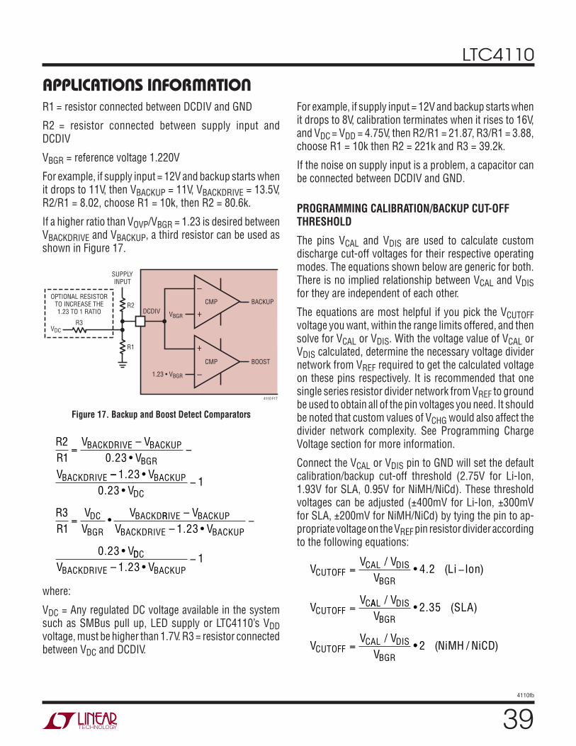
LTC4110
394110fb
R1 = resistor connected between DCDIV and GND
R2 = resistor connected between supply input and DCDIV
VBGR = reference voltage 1.220V
For example, if supply input = 12V and backup starts when it drops to 11V, then VBACKUP = 11V, VBACKDRIVE = 13.5V, R2/R1 = 8.02, choose R1 = 10k, then R2 = 80.6k.
If a higher ratio than VOVP/VBGR = 1.23 is desired between VBACKDRIVE and VBACKUP, a third resistor can be used as shown in Figure 17.
For example, if supply input = 12V and backup starts when it drops to 8V, calibration terminates when it rises to 16V, and VDC = VDD = 4.75V, then R2/R1 = 21.87, R3/R1 = 3.88, choose R1 = 10k then R2 = 221k and R3 = 39.2k.
If the noise on supply input is a problem, a capacitor can be connected between DCDIV and GND.
PROGRAMMING CALIBRATION/BACKUP CUT-OFF THRESHOLD
The pins VCAL and VDIS are used to calculate custom discharge cut-off voltages for their respective operating modes. The equations shown below are generic for both. There is no implied relationship between VCAL and VDIS for they are independent of each other.
The equations are most helpful if you pick the VCUTOFF voltage you want, within the range limits offered, and then solve for VCAL or VDIS. With the voltage value of VCAL or VDIS calculated, determine the necessary voltage divider network from VREF required to get the calculated voltage on these pins respectively. It is recommended that one single series resistor divider network from VREF to ground be used to obtain all of the pin voltages you need. It should be noted that custom values of VCHG would also affect the divider network complexity. See Programming Charge Voltage section for more information.
Connect the VCAL or VDIS pin to GND will set the default calibration/backup cut-off threshold (2.75V for Li-Ion, 1.93V for SLA, 0.95V for NiMH/NiCd). These threshold voltages can be adjusted (±400mV for Li-Ion, ±300mV for SLA, ±200mV for NiMH/NiCd) by tying the pin to ap-propriate voltage on the VREF pin resistor divider according to the following equations:
VV V
VLi Ion
VV
CUTOFFCAL DIS
BGR
CUTOFFC
= −
=
/• . ( )4 2
AAL DIS
BGR
CUTOFFCAL DIS
BGR
VV
SLA
VV V
V
/• . ( )
/
2 35
= •• ( / )2 NiMH NiCD
APPLICATIONS INFORMATION
Figure 17. Backup and Boost Detect Comparators
RR
V VV
V
BACKDRIVE BACKUP
BGR
BACKDRIVE
21 0 23
= −–
. •–– . •
. •
•
1 230 23
1
31
VV
RR
VV
V
BACKUP
DC
DC
BGR
BACKD
−
= RRIVE BACKUP
BACKDRIVE BACKUP
VV V
V
–– . •
. •
1 23
0 23
−
DDC
BACKDRIVE BACKUPV V– . •1 231−
where:
VDC = Any regulated DC voltage available in the system such as SMBus pull up, LED supply or LTC4110’s VDD voltage, must be higher than 1.7V. R3 = resistor connected between VDC and DCDIV.
4110 F17
DCDIV
BACKUP
SUPPLYINPUT –
+VBGR
VDC
R2
R1
R3
OPTIONAL RESISTORTO INCREASE THE1.23 TO 1 RATIO
CMP
BOOST
1.23 • VBGR
+
–CMP
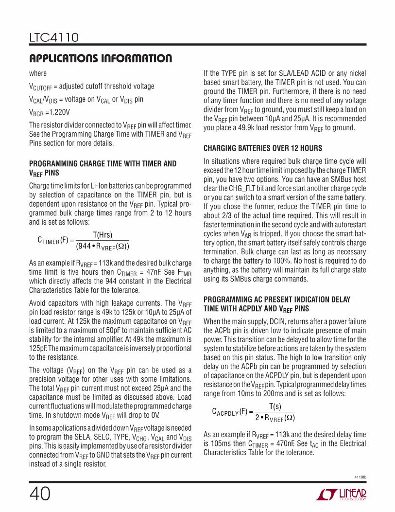
LTC4110
404110fb
If the TYPE pin is set for SLA/LEAD ACID or any nickel based smart battery, the TIMER pin is not used. You can ground the TIMER pin. Furthermore, if there is no need of any timer function and there is no need of any voltage divider from VREF to ground, you must still keep a load on the VREF pin between 10μA and 25μA. It is recommended you place a 49.9k load resistor from VREF to ground.
CHARGING BATTERIES OVER 12 HOURS
In situations where required bulk charge time cycle will exceed the 12 hour time limit imposed by the charge TIMER pin, you have two options. You can have an SMBus host clear the CHG_FLT bit and force start another charge cycle or you can switch to a smart version of the same battery. If you chose the former, reduce the TIMER pin time to about 2/3 of the actual time required. This will result in faster termination in the second cycle and with autorestart cycles when VAR is tripped. If you choose the smart bat-tery option, the smart battery itself safely controls charge termination. Bulk charge can last as long as necessary to charge the battery to 100%. No host is required to do anything, as the battery will maintain its full charge state using its SMBus charge commands.
PROGRAMMING AC PRESENT INDICATION DELAY TIME WITH ACPDLY AND VREF PINS
When the main supply, DCIN, returns after a power failure the ACPb pin is driven low to indicate presence of main power. This transition can be delayed to allow time for the system to stabilize before actions are taken by the system based on this pin status. The high to low transition only delay on the ACPb pin can be programmed by selection of capacitance on the ACPDLY pin, but is dependent upon resistance on the VREF pin. Typical programmed delay times range from 10ms to 200ms and is set as follows:
CACPDLY(F) =
T(s)2 • RVREF(Ω)
As an example if RVREF = 113k and the desired delay time is 105ms then CTIMER = 470nF. See tAC in the Electrical Characteristics Table for the tolerance.
where
VCUTOFF = adjusted cutoff threshold voltage
VCAL/VDIS = voltage on VCAL or VDIS pin
VBGR =1.220V
The resistor divider connected to VREF pin will affect timer. See the Programming Charge Time with TIMER and VREF Pins section for more details.
PROGRAMMING CHARGE TIME WITH TIMER AND VREF PINS
Charge time limits for Li-Ion batteries can be programmed by selection of capacitance on the TIMER pin, but is dependent upon resistance on the VREF pin. Typical pro-grammed bulk charge times range from 2 to 12 hours and is set as follows:
CTIMER(F) =
T(Hrs)(944 • RVREF(Ω))
As an example if RVREF = 113k and the desired bulk charge time limit is fi ve hours then CTIMER = 47nF. See FTMR which directly affects the 944 constant in the Electrical Characteristics Table for the tolerance.
Avoid capacitors with high leakage currents. The VREF pin load resistor range is 49k to 125k or 10μA to 25μA of load current. At 125k the maximum capacitance on VREF is limited to a maximum of 50pF to maintain suffi cient AC stability for the internal amplifi er. At 49k the maximum is 125pF. The maximum capacitance is inversely proportional to the resistance.
The voltage (VREF) on the VREF pin can be used as a precision voltage for other uses with some limitations. The total VREF pin current must not exceed 25μA and the capacitance must be limited as discussed above. Load current fl uctuations will modulate the programmed charge time. In shutdown mode VREF will drop to 0V.
In some applications a divided down VREF voltage is needed to program the SELA, SELC, TYPE, VCHG, VCAL and VDIS pins. This is easily implemented by use of a resistor divider connected from VREF to GND that sets the VREF pin current instead of a single resistor.
APPLICATIONS INFORMATION
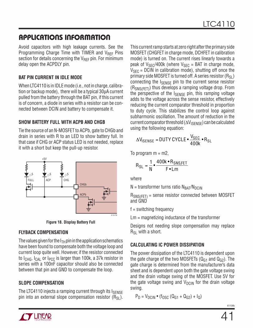
LTC4110
414110fb
Avoid capacitors with high leakage currents. See the Programming Charge Time with TIMER and VREF Pins section for details concerning the VREF pin. For minimum delay open the ACPDLY pin.
BAT PIN CURRENT IN IDLE MODE
When LTC4110 is in IDLE mode (i.e., not in charge, calibra-tion or backup mode), there will be a typical 30μA current pulled from the battery through the BAT pin, if this current is of concern, a diode in series with a resistor can be con-nected between DCIN and battery to compensate it.
SHOW BATTERY FULL WITH ACPB AND CHGB
Tie the source of an N-MOSFET to ACPb, gate to CHGb and drain in series with R to an LED to show battery full. In that case if CHG or ACP status LED is not needed, replace it with a short but keep the pull-up resistor.
This current ramp starts at zero right after the primary side MOSFET (CHGFET in charge mode, DCHFET in calibration mode) is turned on. The current rises linearly towards a peak of VSEC/400k (where VSEC = BAT in charge mode, VSEC = DCIN in calibration mode), shutting off once the primary side MOSFET is turned off. A series resistor (RSL) connecting the ISENSE pin to the current sense resistor (RSNS(FET)) thus develops a ramping voltage drop. From the perspective of the ISENSE pin, this ramping voltage adds to the voltage across the sense resistor, effectively reducing the current comparator threshold in proportion to duty cycle. This stabilizes the control loop against subharmonic oscillation. The amount of reduction in the current comparator threshold (ΔVISENSE) can be calculated using the following equation:
ΔVISENSE = DUTY CYCLE • VSEC
400k• RSL
To program m = m2,
R
Nk RF LmSL
SNS FET=1 400
•••
,
where
N = transformer turns ratio NBAT/NDCIN
RSNS(FET) = sense resistor connected between MOSFET and GND
f = switching frequency
Lm = magnetizing inductance of the transformer
Designs not needing slope compensation may replace RSL with a short.
CALCULATING IC POWER DISSIPATION
The power dissipation of the LTC4110 is dependent upon the gate charge of the two MOSFETs (QG1 and QG2). The gate charge is determined from the manufacturer’s data sheet and is dependent upon both the gate voltage swing and the drain voltage swing of the MOSFET. Use 5V for the gate voltage swing and VDCIN for the drain voltage swing.
PD = VDCIN • (fOSC (QG1 + QG2) + IQ)
APPLICATIONS INFORMATION
Figure 18. Display Battery Full
FULL ACP
+5V
CHG
CHGb
ACPb
4110 F18
FLYBACK COMPENSATION
The values given for the ITH pin in the application schematics have been found to compensate both the voltage loop and current loop quite well. However, if the resistor connected to ICHG, ICAL or IPCC is larger than 100k, a 37k resistor in series with a 100nF capacitor should also be connected between that pin and GND to compensate the loop.
SLOPE COMPENSATION
The LTC4110 injects a ramping current through its ISENSE pin into an external slope compensation resistor (RSL).
LTC4110
424110fb
Example:
VDCIN = 12V, fOSC = 300kHz, QG1 = QG2 = 15nC, IQ = 3mA
PD = 144mW
SNUBBER DESIGN
The values given in the applications schematics have been found to work quite well for this 12V-1A application. Care should be taken in selecting other values for your applica-tion since effi ciency may be impacted by a poor choice. For a detailed look at snubber design, Application Note 19 is very helpful.
COMPONENT SELECTION
Current Sense Resistors
The LTC4110 uses up to three sense resistors—one of them optional. In general, current sense resistors should have a low temperature coeffi cient and suffi cient power dissipation capability to avoid self-heating. Tolerance depends on system accuracy requirements.
RSNS(FET): The power rating of RSNS(FET) is defi ned by the highest value between ICHG or ICAL and the transformer turns ratio. Use one the following equations to calculate IRSNS(FET) depending on which value, ICHG or ICAL which-ever is higher.
IR(SNSFETCHG) =
ICHG • 1+ VBATN•VDCIN
N•VBAT
E2 •VDCIN+1
IR(SNSFETCAL) =
ICAL • 1+ VBATN•VDCIN
N•E2 •VBATVDCIN
+1
Plug in the higher value of the above two results as IR(SNSFET) and solve for power:
PR(SNSFET) = IR(SNSFET)2 • RSNS(FET)
RCL: RCL power rating is a function of the maximum forward current the system load draws. See Figure 11.
PR(CL) = IMAX2 • RCL
Find a sense resistor who’s power rating is greater than PR(CL)
RSNS(BAT): RSNS(BAT) power rating is a function of the highest current value between ICHG or ICAL with which the battery will work. Plug in the higher of the two into IBAT(MAX) and solve:
PR(SNSBAT) = IMAX2 • RSNS(BAT)
Use a sense resistor with a power rating greater than PSNS(BAT)
FLYBACK MOSFET SELECTION
The LTC4110 uses two low side N-channel switching MOSFETs in its fl yback converter. These MOSFETs have dual roles. An any given time, only one MOSFET is the primary switch while the other acts as a synchronous recti-fi er on the secondary to improve effi ciency. The individual MOSFETs’ roles depend on whether the battery is being charged or calibrated. Each MOSFET specifi cation must account for both roles.
The MOSFET voltage ratings in a fl yback design must deal with other factors beyond VIN. During switch “on” time, a current is established in the primary leakage inductance (LL) equal to peak primary current (IPRI). When the switch turns off, the energy stored in LL, (Energy = IPRI
2 • LL/2) causes the switch voltage to fl y up, starting from the input voltage on up to the breakdown of the MOSFET if the volt-age is not clamped. Thus, the snubber design is critical in dealing with this voltage spike and can infl uence the MOSFET voltage selection value. From a MOSFET point of view, the minimum voltage must be greater than the snubber clamp voltage VSNUB. If VSNUB itself is too low, zener clamp dissipation rises rapidly thus encouraging higher MOSFET voltages. The maximum DC voltage that the N-channel MOSFETs sees is:
V V
VNCHG FET DCINBAT
( ) = +
V V N VCAL FET BAT DCIN( ) = + •
APPLICATIONS INFORMATION
LTC4110
434110fb
The VDS ratings of the MOSFETs need to be higher than these values.
The MOSFET current ratings for the primary side must be higher than IPRI, which is IPRI(CHG) or IPRI(CAL) for charge and Calibration mode respectively. See Equations 1 and 2. MOSFET current ratings for the secondary side must be higher than IPRI/N. Since both MOSFETs must perform both roles, the minimum current rating of the MOSFETs should be greater than the higher of these values.
MOSFET power dissipation is a function of the RMS cur-rent fl owing through the MOSFET.
Charge Mode:
I
IE
V V N VV
PRI FETCHG
CHG BAT BAT DCIN
DCIN
( )
( )
=
•• + •
I IV N V
N VSEC FETCHG CHGBAT DCIN
DCIN( ) = •
+ •
•
Calibration Mode:
I IV N V
N VPRI FETCAL CALBAT DCIN
DCIN( ) = •
+ •
•
I
I EV V N V
V
SEC FETCAL
CALBAT BAT DCIN
DCI
( )
( )
=
• •• + •
NN
Where IPRI(FETCHG) is the same FET as ISEC(FETCAL) and IPRI(FETCAL) is the same FET as ISEC(FETCHG).
Using the equation below, plug in the higher current from above into IFET to fi nd each FET’s power dissipation for the given mode.
PFET = IFET2 • RDS(ON)
The RDS(ON) value of the MOSFET depends on VGS. Conser-vatively you can use the RDS(ON) value with a VGS rating of 4.5V. If you are using a dual-MOSFET package, determine whether charge mode or calibration mode results is the highest overall power dissipation and use that as the rating for the dual MOSFET.
The MOSFET should be specifi ed for fast or PWM switching. The MOSFET that meets all the above specifi cations but has the lowest QG and/or QGD is often the best choice.
PowerPath MOSFET SELECTION
Important parameters for the selection of PowerPath MOSFETS are the maximum drain-source voltage VDS(MAX), threshold voltage VGS(VT), on-resistance RDS(ON) and QGATE.
The maximum allowable drain-source voltage, VDS(MAX), must be high enough to withstand the maximum drain-source voltage seen in the application.
The gates of these MOSFETs are driven by the INID (Input Ideal Diode) and BATID (Battery Ideal Diode) pins. The gate turn-on voltage, VGS, is set by the smaller of the PowerPath supply voltage or the internal clamping volt-age VGON. For the MOSFET driven from the INID pin its PowerPath supply voltage is the higher of the DCIN pin or DCOUT pin voltage. For the MOSFETs driven from the BATID pin, their PowerPath supply voltage is the higher of the DCOUT pin or BAT pin voltage. Logic-level VGS(VT) MOSFET is commonly used, but if a low supply voltage limits the gate voltage a sub-logic-level threshold MOSFET should be considered.
As a general rule, select a MOSFET with a low enough RDS(ON) to obtain the desired VDS while operating at full current load and an achievable VGS. The MOSFET normally operates in the linear region and acts like a voltage con-trolled resistor. If the MOSFET is grossly undersized then it can enter the saturation region and a large VDS may result. However, the drain-source diode of the MOSFET, if forward biased will limit VDS. A large VDS combined with the load current could result in excessively high MOSFET power dissipation. Keep in mind that the LTC4110 will regulate the forward voltage drop across the MOSFETs at 20mV (VFR) if RDS(ON) is low enough. The required RDS(ON) can be calculated by dividing 0.02V by the load current in amps. Achieving forward regulation will minimize power loss and heat dissipation, but it is not a necessity. If a forward volt-age drop of more than 20mV is acceptable then a smaller MOSFET can be used, but must be sized compatible with the higher power dissipation. Care should be taken to ensure
APPLICATIONS INFORMATION
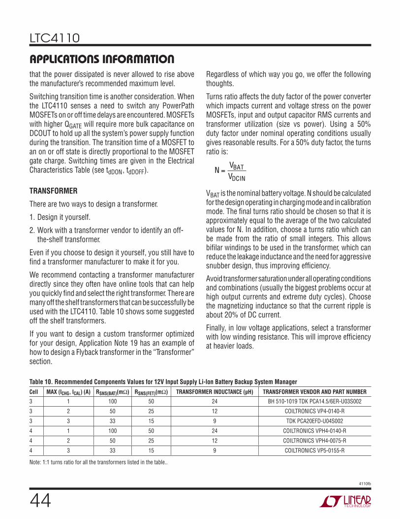
LTC4110
444110fb
Table 10. Recommended Components Values for 12V Input Supply Li-Ion Battery Backup System Manager
Cell MAX (ICHG, ICAL) (A) RSNS(BAT)(mΩ) RSNS(FET)(mΩ) TRANSFORMER INDUCTANCE (μH) TRANSFORMER VENDOR AND PART NUMBER
3 1 100 50 24 BH 510-1019 TDK PCA14.5/6ER-U03S002
3 2 50 25 12 COILTRONICS VP4-0140-R
3 3 33 15 9 TDK PCA20EFD-U04S002
4 1 100 50 24 COILTRONICS VPH4-0140-R
4 2 50 25 12 COILTRONICS VPH4-0075-R
4 3 33 15 9 COILTRONICS VP5-0155-R
Note: 1:1 turns ratio for all the transformers listed in the table..
that the power dissipated is never allowed to rise above the manufacturer’s recommended maximum level.
Switching transition time is another consideration. When the LTC4110 senses a need to switch any PowerPath MOSFETs on or off time delays are encountered. MOSFETs with higher QGATE will require more bulk capacitance on DCOUT to hold up all the system’s power supply function during the transition. The transition time of a MOSFET to an on or off state is directly proportional to the MOSFET gate charge. Switching times are given in the Electrical Characteristics Table (see tdDON, tdDOFF).
TRANSFORMER
There are two ways to design a transformer.
1. Design it yourself.
2. Work with a transformer vendor to identify an off-the-shelf transformer.
Even if you choose to design it yourself, you still have to fi nd a transformer manufacturer to make it for you.
We recommend contacting a transformer manufacturer directly since they often have online tools that can help you quickly fi nd and select the right transformer. There are many off the shelf transformers that can be successfully be used with the LTC4110. Table 10 shows some suggested off the shelf transformers.
If you want to design a custom transformer optimized for your design, Application Note 19 has an example of how to design a Flyback transformer in the “Transformer” section.
APPLICATIONS INFORMATIONRegardless of which way you go, we offer the following thoughts.
Turns ratio affects the duty factor of the power converter which impacts current and voltage stress on the power MOSFETs, input and output capacitor RMS currents and transformer utilization (size vs power). Using a 50% duty factor under nominal operating conditions usually gives reasonable results. For a 50% duty factor, the turns ratio is:
NVV
BAT
DCIN=
VBAT is the nominal battery voltage. N should be calculated for the design operating in charging mode and in calibration mode. The fi nal turns ratio should be chosen so that it is approximately equal to the average of the two calculated values for N. In addition, choose a turns ratio which can be made from the ratio of small integers. This allows bifi lar windings to be used in the transformer, which can reduce the leakage inductance and the need for aggressive snubber design, thus improving effi ciency.
Avoid transformer saturation under all operating conditions and combinations (usually the biggest problems occur at high output currents and extreme duty cycles). Choose the magnetizing inductance so that the current ripple is about 20% of DC current.
Finally, in low voltage applications, select a transformer with low winding resistance. This will improve effi ciency at heavier loads.
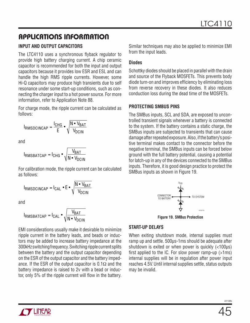
LTC4110
454110fb
Figure 19. SMBus Protection
CONNECTORTO BATTERY
TO SYSTEM
4110 F19
VDD
INPUT AND OUTPUT CAPACITORS
The LTC4110 uses a synchronous fl yback regulator to provide high battery charging current. A chip ceramic capacitor is recommended for both the input and output capacitors because it provides low ESR and ESL and can handle the high RMS ripple currents. However, some Hi-Q capacitors may produce high transients due to self resonance under some start-up conditions, such as con-necting the charger input to a hot power source. For more information, refer to Application Note 88.
For charge mode, the ripple current can be calculated as follows:
II
EN V
VRMSDCINCAPCHG BAT
DCIN= •
•
and
I IV
N VRMSBATCAP CHGBAT
DCIN= •
•
For calibration mode, the ripple current can be calculated as follows:
I I EN V
VRMSDCINCAP CALBAT
DCIN= • •
•
and
I IV
N VRMSBATCAP CALBAT
DCIN= •
•
EMI considerations usually make it desirable to minimize ripple current in the battery leads, and beads or induc-tors may be added to increase battery impedance at the 300kHz switching frequency. Switching ripple current splits between the battery and the output capacitor depending on the ESR of the output capacitor and the battery imped-ance. If the ESR of the output capacitor is 0.1Ω and the battery impedance is raised to 2v with a bead or induc-tor, only 5% of the ripple current will fl ow in the battery.
APPLICATIONS INFORMATIONSimilar techniques may also be applied to minimize EMI from the input leads.
Diodes
Schottky diodes should be placed in parallel with the drain and source of the Flyback MOSFETs. This prevents body diode turn-on and improves effi ciency by eliminating loss from reverse recovery in these diodes. It also reduces conduction loss during the dead time of the MOSFETs.
PROTECTING SMBUS PINS
The SMBus inputs, SCL and SDA, are exposed to uncon-trolled transient signals whenever a battery is connected to the system. If the battery contains a static charge, the SMBus inputs are subjected to transients that can cause damage after repeated exposure. Also, if the battery’s posi-tive terminal makes contact to the connector before the negative terminal, the SMBus inputs can be forced below ground with the full battery potential, causing a potential for latch-up in any of the devices connected to the SMBus inputs. Therefore, it is good design practice to protect the SMBus inputs as shown in Figure 19.
START-UP DELAYS
When exiting shutdown mode, internal supplies must ramp up and settle. 500μs-1ms should be adequate after shutdown is exited or when power is quickly (<100μs) fi rst applied to the IC. For slow power ramp-up (>1ms) internal supplies will be in regulation after power input reaches 4.5V. Until internal supplies settle, status outputs may be invalid.
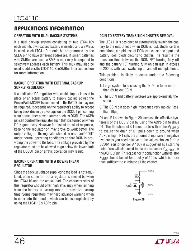
LTC4110
464110fb
APPLICATIONS INFORMATIONOPERATION WITH DUAL BACKUP SYSTEMS
If a dual backup system consisting of two LTC4110s each with its own backup battery is needed and a SMBus is used, each LTC4110 should be programmed by the SELA pin to have different addresses. If smart batteries with SMBus are used, a SMBus mux may be required to selectively address each battery. This mux may also be used to address the LTC4110. See SMBus Interface section for more information.
BACKUP OPERATION WITH EXTERNAL BACKUP SUPPLY REGULATOR
If a dedicated DC regulator with enable inputs is used in place of an actual battery to supply backup power, the PowerPath MOSFETs connected to the BATID pin may not be required. It depends on the regulator’s ability to accept being back driven by a voltage on the DCOUT pin coming from some other power source such as DCIN. The ACPb pin can control the regulator such that it is turned on when DCIN goes away. However for fastest transient response, keeping the regulator on may prove to work better. The output voltage of the regulator should be less than DCOUT under normal operating conditions so that DCIN is pro-viding the power to the load. The voltage provided by the regulator must not be allowed to go below the lower limit of the DCOUT pin or erratic operation may result.
BACKUP OPERATION WITH A DOWNSTREAM REGULATOR
Since the backup voltage supplied to the load is not regu-lated, often some form of a regulator is needed between the LTC4110 and the actual load. The characteristics of this regulator should offer high effi ciency when running from the battery in backup mode to maximize backup time. Some regulators may need advance warning when to enter into this mode, which can be accomplished by using the LTC4110’s ACPb pin.
DCIN TO BATTERY TRANSITION CHATTER REMOVAL
The LTC4110 is designed to automatically switch the bat-tery to the output load when DCIN is lost. Under certain conditions, a rapid loss of DCIN can cause the input and battery ideal diode circuits to chatter. The result is the transition time between the DCIN FET turning fully off and the battery FET turning fully on can last in excess of 200ms with each switching on and off multiple times.
This problem is likely to occur under the following conditions:
1. Large system load causing the INID pin to be more than 3V below DCIN.
2. The DCIN and battery voltages are approximately the same.
3. The DCIN pin goes high impedance very rapidly (less than 10μs)
Q1 and R1 shown in Figure 20 increase the effective hys-teresis of the DCDIV pin by using the ACPb pin to drive Q1. The threshold of Q1 must be less than the VSUPPLY
to assure the drain of Q1 pulls down to ground when ACPb is high. R1 sets the amount of increase in negative hysteresis you need relative to the values chosen for the DCDIV resistor divider. A 100k is suggested as a starting point. You will also need to place a capacitor CACPDLY on the ACPDLY pin. This capacitor in conjunction with resistor RVREF should be set for a delay of 10ms, which is more than suffi cient to eliminate all the chatter.
Figure 20.
Q12N7002
R1100k
DCDIV
ACPb
4110 F20
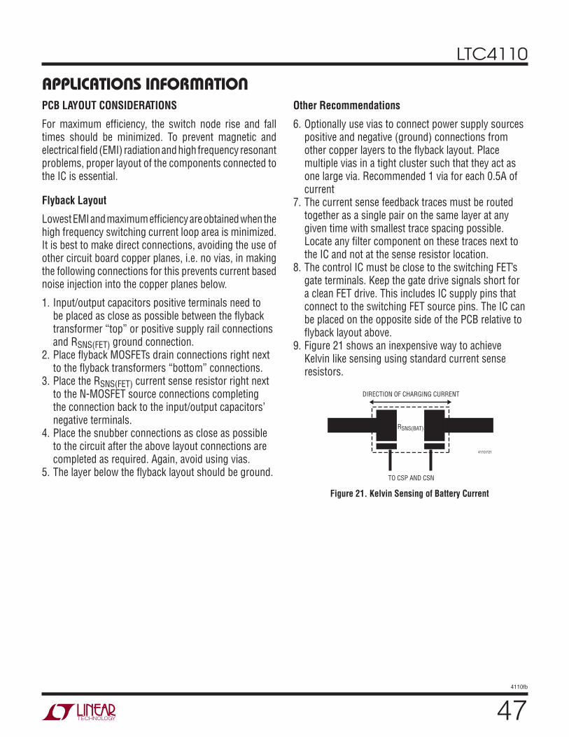
LTC4110
474110fb
PCB LAYOUT CONSIDERATIONS
For maximum effi ciency, the switch node rise and fall times should be minimized. To prevent magnetic and electrical fi eld (EMI) radiation and high frequency resonant problems, proper layout of the components connected to the IC is essential.
Flyback Layout
Lowest EMI and maximum effi ciency are obtained when the high frequency switching current loop area is minimized. It is best to make direct connections, avoiding the use of other circuit board copper planes, i.e. no vias, in making the following connections for this prevents current based noise injection into the copper planes below.
1. Input/output capacitors positive terminals need to be placed as close as possible between the fl yback transformer “top” or positive supply rail connections and RSNS(FET) ground connection.
2. Place fl yback MOSFETs drain connections right next to the fl yback transformers “bottom” connections.
3. Place the RSNS(FET) current sense resistor right next to the N-MOSFET source connections completing the connection back to the input/output capacitors’ negative terminals.
4. Place the snubber connections as close as possible to the circuit after the above layout connections are completed as required. Again, avoid using vias.
5. The layer below the fl yback layout should be ground.
Other Recommendations
6. Optionally use vias to connect power supply sources positive and negative (ground) connections from other copper layers to the fl yback layout. Place multiple vias in a tight cluster such that they act as one large via. Recommended 1 via for each 0.5A of current
7. The current sense feedback traces must be routed together as a single pair on the same layer at any given time with smallest trace spacing possible. Locate any fi lter component on these traces next to the IC and not at the sense resistor location.
8. The control IC must be close to the switching FET’s gate terminals. Keep the gate drive signals short for a clean FET drive. This includes IC supply pins that connect to the switching FET source pins. The IC can be placed on the opposite side of the PCB relative to fl yback layout above.
9. Figure 21 shows an inexpensive way to achieve Kelvin like sensing using standard current sense resistors.
APPLICATIONS INFORMATION
TO CSP AND CSN
4110 F21
DIRECTION OF CHARGING CURRENT
RSNS(BAT)
Figure 21. Kelvin Sensing of Battery Current
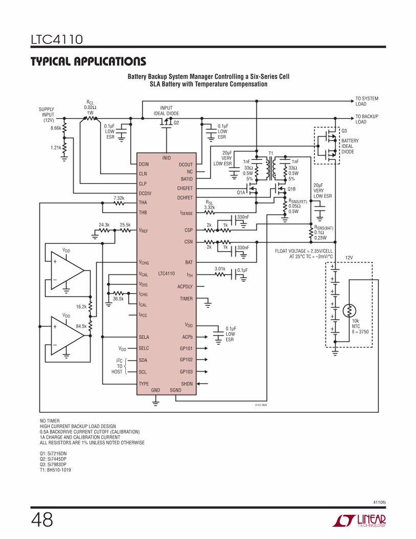
LTC4110
484110fb
TYPICAL APPLICATIONSBattery Backup System Manager Controlling a Six-Series Cell
SLA Battery with Temperature Compensation
DCIN
INID
CLN
CLP
DCDIV7.32k
1.21k
8.66k
24.3k
RSNS(FET)0.05Ω0.5W
33Ω0.5W5%
33Ω0.5W
5%
RSL3.32k
RCL0.02Ω
1W
3.01k 0.1μF
1k2k 330nF
1nF1nF
1k2k
330nF
RSNS(BAT)0.1Ω0.25W
THA
THB
VREF
10kNTCß = 3750
I2CTO
HOST
0.1μFLOWESR
NO TIMERHIGH CURRENT BACKUP LOAD DESIGN0.5A BACKDRIVE CURRENT CUTOFF (CALIBRATION)1A CHARGE AND CALIBRATION CURRENTALL RESISTORS ARE 1% UNLESS NOTED OTHERWISE
Q1: Si7216DNQ2: Si7445DPQ3: Si7983DPT1: BH510-1019
20μFVERYLOW ESR
BATTERYIDEALDIODE
INPUTIDEAL DIODE
Q2
TO SYSTEMLOAD
TO BACKUPLOAD
12VVCHG
VCAL
VDIS
VDD
ICHG
ICAL
IPCC
SELA
SELC
SDA
SCL
TYPE
DCOUT
SUPPLYINPUT(12V)
NC
BATID
CHGFET
DCHFET
ISENSE
CSP
CSN
BAT
ITH
ACPDLY
TIMER
VDD
ACPb
GP101
GP102
GP103
SHDN
GND SGND
20μFVERY
LOW ESR
25.5k
+
+
+
+
+
+
4110 TA04
FLOAT VOLTAGE = 2.35V/CELLAT 25°C TC = –2mV/°C
LTC4110
0.1μFLOWESR
0.1μFLOWESR
–
+
VDD
–
+ 84.5k
16.2k
Q3
Q1AQ1B
T1
36.5k
VDD
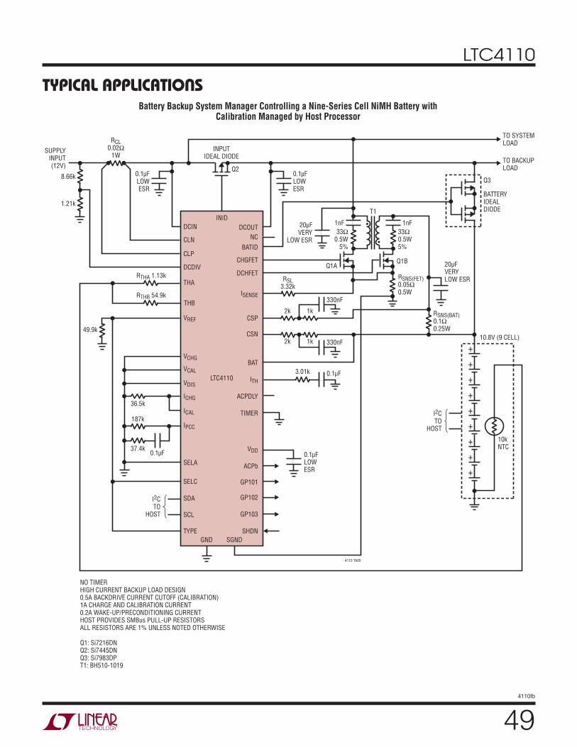
LTC4110
494110fb
TYPICAL APPLICATIONSBattery Backup System Manager Controlling a Nine-Series Cell NiMH Battery with
Calibration Managed by Host Processor
DCIN
INID
CLN
CLP
DCDIV
THA
VREF
10kNTC
I2CTO
HOST
0.1μFLOWESR
20μFVERYLOW ESR
BATTERYIDEALDIODE
INPUTIDEAL DIODE
TO SYSTEMLOAD
TO BACKUPLOAD
VCHG
VCAL
VDIS
ICHG
ICAL
IPCC
SELA
SELC
SDA
SCL
TYPE
DCOUT
SUPPLYINPUT(12V)
NC
BATID
CHGFET
DCHFET
ISENSE
CSP
CSN
BAT
ITH
ACPDLY
TIMER
VDD
ACPb
GP101
GP102
GP103
SHDN
GND SGND
20μFVERY
LOW ESR
+
+
+
+
+
+
+
+
+
I2CTO
HOST
4110 TA05
LTC4110
0.1μFLOWESR
0.1μFLOWESR
THB
RTHA 1.13k
RTHB 54.9k
1.21k
49.9k
8.66k
RSNS(FET)0.05Ω0.5W
33Ω0.5W5%
33Ω0.5W
5%
RSL3.32k
RCL0.02Ω
1W
3.01k 0.1μF
0.1μF
1k2k 330nF
1nF1nF
1k2k
330nF
RSNS(BAT)0.1Ω0.25W
NO TIMERHIGH CURRENT BACKUP LOAD DESIGN0.5A BACKDRIVE CURRENT CUTOFF (CALIBRATION)1A CHARGE AND CALIBRATION CURRENT0.2A WAKE-UP/PRECONDITIONING CURRENTHOST PROVIDES SMBus PULL-UP RESISTORSALL RESISTORS ARE 1% UNLESS NOTED OTHERWISE
Q1: Si7216DNQ2: Si7445DNQ3: Si7983DPT1: BH510-1019
Q2
Q3
Q1AQ1B
36.5k
187k
37.4k
10.8V (9 CELL)
T1
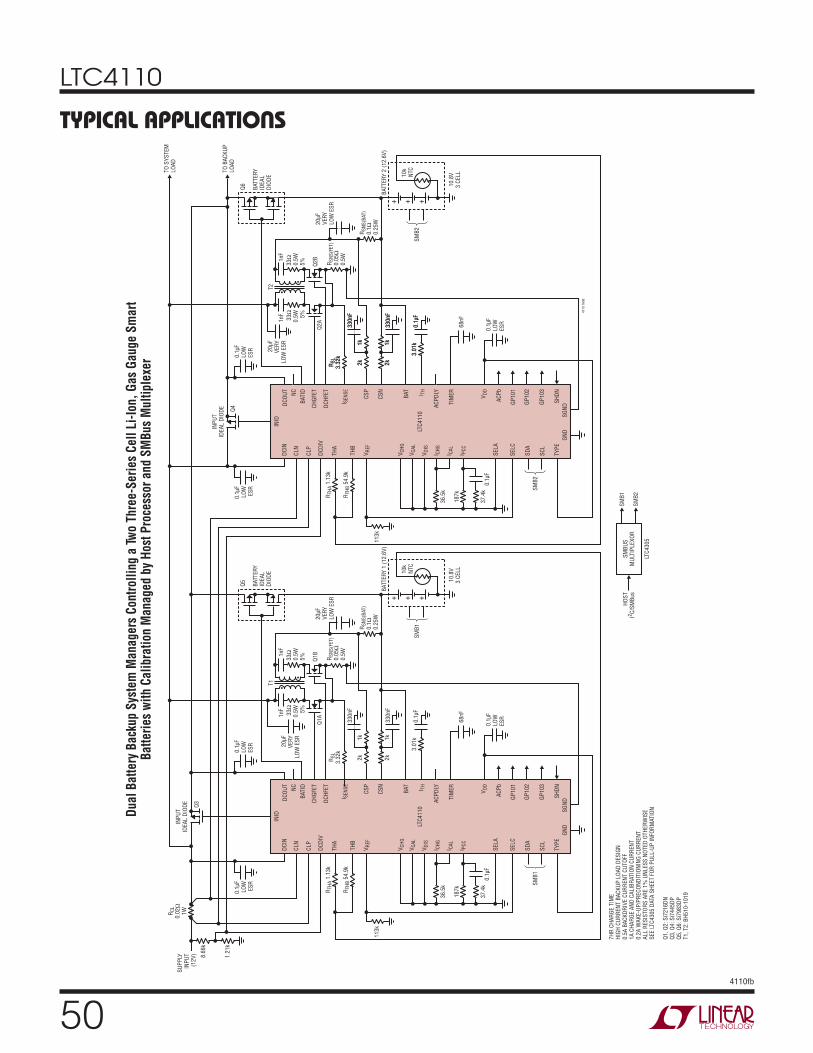
LTC4110
504110fb
TYPICAL APPLICATIONSD
ual
Bat
tery
Bac
kup
Sys
tem
Man
ager
s C
ontr
olli
ng a
Tw
o Th
ree-
Ser
ies
Cel
l Li
-Ion
, G
as G
auge
Sm
art
Bat
teri
es w
ith
Cal
ibra
tion
Man
aged
by
Hos
t P
roce
ssor
and
SM
Bus
Mul
tipl
exer
DC
IN
INID
CLN
CLP
DC
DIV
TH
A
VR
EF
10k
NTC
SM
B2
SM
B1
SM
B2
SM
B1
0.1
μF
LO
WES
R
20μF
VER
YLO
W E
SR
BA
TTER
YID
EA
LD
IOD
E
INP
UT
IDEA
L D
IOD
ETO
BA
CK
UP
LO
AD
SELC
SD
A
SC
L
TYP
E
DC
OU
T
NC
BA
TID
CH
GFE
T
DC
HFE
T
I SE
NS
E
CS
P
CS
N
BA
T
I TH
AC
PD
LY
TIM
ER
VD
D
AC
Pb
GP
101
GP
102
GP
103
SH
DN
GN
DS
GN
D
20μF
VER
YLO
W E
SR
+ + +S
MB
2
4110 T
A06
LTC
4110
0.1
μF
LO
WES
R
0.1
μF
LO
WES
R
TH
B
RT
HA 1
.13k
RT
HB 5
4.9
k
DC
IN
INID
CLN
CLP
DC
DIV
TH
A
VR
EF
10k
NTC
BA
TTER
Y 2
(12.6
V)
10.8
V3 C
ELL
10.8
V3 C
ELL
BA
TTER
Y 1
(12.6
V)
0.1
μF
LO
WES
R
20μF
VER
YLO
W E
SR
BA
TTER
YID
EA
LD
IOD
E
INP
UT
IDEA
L D
IOD
E
TO
SY
STEM
LO
AD
SELC
SD
A
SC
L
TYP
E
DC
OU
T
SU
PP
LYIN
PU
T(1
2V
)
NC
BA
TID
CH
GFE
T
DC
HFE
T
I SE
NS
E
CS
P
CS
N
BA
T
I TH
AC
PD
LY
TIM
ER
VD
D
AC
Pb
GP
101
GP
102
GP
103
SH
DN
GN
DS
GN
D
20μF
VER
YLO
W E
SR
+ + +S
MB
1
SM
BU
SM
ULT
IPL
EX
OR
HO
ST
I2C
/SM
Bus
LTC
4305
LTC
41
10
0.1
μF
LO
WES
R
0.1
μF
LO
WES
R
TH
B
RT
HA 1
.13k
RT
HB 5
4.9
k
VC
HG
VC
AL
VD
IS
I CH
G
I CA
L
I PC
C
SELA
1.2
1k
113k
8.6
6k
RC
L0.0
2Ω
1W
0.1
μF
7H
R C
HA
RG
E T
IME
HIG
H C
UR
RE
NT
BA
CK
UP
LO
AD
DE
SIG
N0.5
A B
AC
KD
RIV
E C
UR
REN
T C
UTO
FF1
A C
HA
RG
E A
ND
CA
LIB
RA
TIO
N C
UR
RE
NT
0.2
A W
AK
E-U
P/P
RE
CO
ND
ITIO
NIN
G C
UR
RE
NT
AL
L R
ES
IST
OR
S A
RE
1%
UN
LE
SS
NO
TE
D O
TH
ER
WIS
ES
EE L
TC
4305 D
ATA
SH
EET F
OR
PU
LL-U
P I
NFO
RM
ATIO
N
Q1
, Q
2: S
i72
16
DN
Q3
, Q
4: S
i74
45
DP
Q5, Q
6: S
i7983D
PT
1,
T2
: B
H5
10
-10
19
Q3
37.4
k
36.5
k
187k
VC
HG
VC
AL
VD
IS
I CH
G
I CA
L
I PC
C
SELA
113k
0.1
μF
37.4
k
36.5
k
187k
RS
NS
(FE
T)
0.0
5Ω
0.5
W
33Ω
0.5
W5%
33Ω
0.5
W5%
RS
L3.3
2k 3
.01k
0.1
μF
68nF
1k
2k
330nF
1nF
1nF
1k
2k
330nF
RS
NS
(BA
T)
0.1
Ω0.2
5W
Q5
Q1A
Q1B
RS
L3.3
2k 3
.01k
0.1
μF
1k
2k
330nF
1k
2k
330nF
Q6
RS
NS
(FE
T)
0.0
5Ω
0.5
W
33Ω
0.5
W5%
33Ω
0.5
W5%
RS
L3.3
2k 3
.01k
0.1
μF
68nF
1k
2k
330nF
1nF
1nF
1k
2k
330nF
RS
NS
(BA
T)
0.1
Ω0.2
5W
Q2A
Q2B
Q4
T2
T1
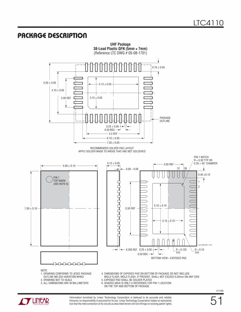
LTC4110
514110fb
Information furnished by Linear Technology Corporation is believed to be accurate and reliable. However, no responsibility is assumed for its use. Linear Technology Corporation makes no representa-tion that the interconnection of its circuits as described herein will not infringe on existing patent rights.
PACKAGE DESCRIPTIONUHF Package
38-Lead Plastic QFN (5mm × 7mm)(Reference LTC DWG # 05-08-1701)
5.00 0.10
NOTE:1. DRAWING CONFORMS TO JEDEC PACKAGE OUTLINE M0-220 VARIATION WHKD2. DRAWING NOT TO SCALE3. ALL DIMENSIONS ARE IN MILLIMETERS
PIN 1TOP MARK(SEE NOTE 6)
37
1
2
38
BOTTOM VIEW—EXPOSED PAD
5.50 REF5.15 ± 0.10
7.00 0.10
0.75 0.05
R = 0.125TYP
R = 0.10TYP
0.25 0.05
(UH) QFN REF C 1107
0.50 BSC
0.200 REF
0.00 – 0.05
RECOMMENDED SOLDER PAD LAYOUTAPPLY SOLDER MASK TO AREAS THAT ARE NOT SOLDERED
3.00 REF
3.15 ± 0.10
0.40 0.10
0.70 0.05
0.50 BSC
5.5 REF
3.00 REF 3.15 ± 0.05
4.10 0.05
5.50 0.055.15 ± 0.05
6.10 0.05
7.50 0.05
0.25 0.05
PACKAGEOUTLINE
4. DIMENSIONS OF EXPOSED PAD ON BOTTOM OF PACKAGE DO NOT INCLUDE MOLD FLASH. MOLD FLASH, IF PRESENT, SHALL NOT EXCEED 0.20mm ON ANY SIDE5. EXPOSED PAD SHALL BE SOLDER PLATED6. SHADED AREA IS ONLY A REFERENCE FOR PIN 1 LOCATION ON THE TOP AND BOTTOM OF PACKAGE
PIN 1 NOTCHR = 0.30 TYP OR0.35 45 CHAMFER
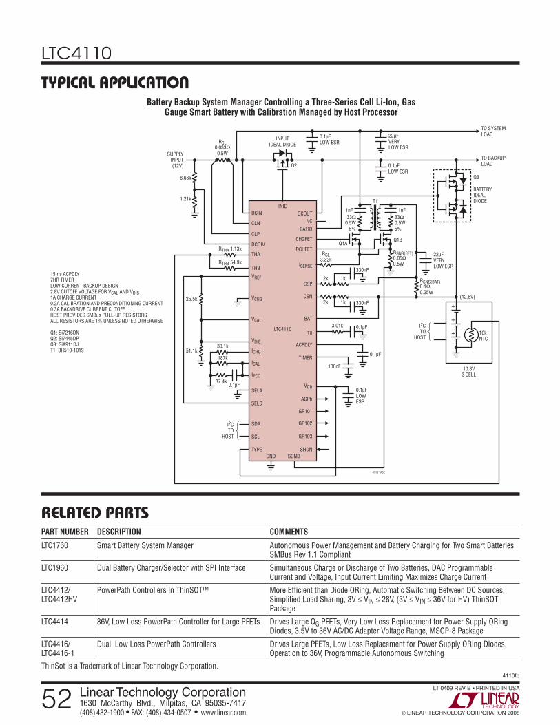
LTC4110
524110fb
Linear Technology Corporation1630 McCarthy Blvd., Milpitas, CA 95035-7417 (408) 432-1900 ● FAX: (408) 434-0507 ● www.linear.com © LINEAR TECHNOLOGY CORPORATION 2008
LT 0409 REV B • PRINTED IN USA
TYPICAL APPLICATIONBattery Backup System Manager Controlling a Three-Series Cell Li-Ion, Gas
Gauge Smart Battery with Calibration Managed by Host Processor
RELATED PARTSPART NUMBER DESCRIPTION COMMENTS
LTC1760 Smart Battery System Manager Autonomous Power Management and Battery Charging for Two Smart Batteries, SMBus Rev 1.1 Compliant
LTC1960 Dual Battery Charger/Selector with SPI Interface Simultaneous Charge or Discharge of Two Batteries, DAC Programmable Current and Voltage, Input Current Limiting Maximizes Charge Current
LTC4412/LTC4412HV
PowerPath Controllers in ThinSOT™ More Effi cient than Diode ORing, Automatic Switching Between DC Sources, Simplifi ed Load Sharing, 3V ≤ VIN ≤ 28V, (3V ≤ VIN ≤ 36V for HV) ThinSOT Package
LTC4414 36V, Low Loss PowerPath Controller for Large PFETs Drives Large QG PFETs, Very Low Loss Replacement for Power Supply ORing Diodes, 3.5V to 36V AC/DC Adapter Voltage Range, MSOP-8 Package
LTC4416/LTC4416-1
Dual, Low Loss PowerPath Controllers Drives Large PFETs, Low Loss Replacement for Power Supply ORing Diodes, Operation to 36V, Programmable Autonomous Switching
ThinSot is a Trademark of Linear Technology Corporation.
RSNS(BAT)0.1Ω0.25W
DCIN
INID
CLN
CLP
DCDIVRTHA 1.13k
THA
THB
VREF
10kNTC
I2CTO
HOST
0.1μFLOWESR
22μFVERYLOW ESR
0.1μFLOW ESR
BATTERYIDEALDIODE
INPUTIDEAL DIODE
TO SYSTEMLOAD
TO BACKUPLOAD
VCHG
VCAL
VDIS
ICHG
ICAL
IPCC
SELA
SELC
SDA
SCL
TYPE
DCOUT
SUPPLYINPUT(12V)
NC
BATID
CHGFET
DCHFET
ISENSE
CSP
CSN
BAT
ITH
ACPDLY
TIMER
VDD
ACPb
GP101
GP102
GP103
SHDN
GND SGND
RTHB 54.9k
0.1μFLOW ESR
22μFVERYLOW ESR
+
+
+I2CTO
HOST
4110 TA02
(12.6V)
LTC4110
1.21k
25.5k
51.1k
8.66k
RCL0.033Ω0.5W
0.1μF
Q2
30.1k
187k
37.4k
RSNS(FET)0.05Ω0.5W
33Ω0.5W5%
33Ω0.5W
5%
RSL3.32k
3.01k 0.1μF
1k2k 330nF
1nF1nF
1k2k
330nF
Q3
Q1AQ1B
T1
10.8V3 CELL
0.1μF
100nF
15ms ACPDLY7HR TIMERLOW CURRENT BACKUP DESIGN2.8V CUTOFF VOLTAGE FOR VCAL AND VDIS1A CHARGE CURRENT0.2A CALIBRATION AND PRECONDITIONING CURRENT0.3A BACKDRIVE CURRENT CUTOFFHOST PROVIDES SMBus PULL-UP RESISTORSALL RESISTORS ARE 1% UNLESS NOTED OTHERWISE
Q1: Si7216DNQ2: Si7445DPQ3: SiA911DJT1: BH510-1019