Embed Size (px)
Citation preview
LT4356-1/LT4356-2
14356fb
For more information www.linear.com/LT4356-1
ApplicAtions
FeAtures Description
Surge Stopper
The LT®4356 surge stopper protects loads from high voltage transients. It regulates the output during an overvoltage event, such as load dump in automobiles, by controlling the gate of an external N-channel MOSFET. The output is limited to a safe value thereby allowing the loads to con-tinue functioning. The LT4356 also monitors the voltage drop between the VCC and SNS pins to protect against overcurrent faults. An internal amplifier limits the current sense voltage to 50mV. In either fault condition, a timer is started inversely proportional to MOSFET stress. If the timer expires, the FLT pin pulls low to warn of an impend-ing power down. If the condition persists, the MOSFET is turned off. After a cool down period, the GATE pin pulls up turning on the MOSFET again.
The auxiliary amplifier may be used as a voltage detection comparator or as a linear regulator controller driving an external PNP pass transistor.
Back-to-back FETs can be used in lieu of a Schottky diode for reverse input protection, reducing voltage drop and power loss. A shutdown pin reduces the quiescent current to less than 7µA for the LT4356-1 during shutdown. The LT4356-2 differs from the LT4356-1 during shutdown by reducing the quiescent current to 60µA and keeping alive the auxiliary amplifier for uses such as an undervoltage lockout or always-on regulator.
n Automotive/Avionic Surge Protectionn Hot Swap/Live Insertionn High Side Switch for Battery Powered Systemsn Intrinsic Safety Applications
n Stops High Voltage Surgesn Adjustable Output Clamp Voltagen Overcurrent Protectionn Wide Operation Range: 4V to 80Vn Reverse Input Protection to –60Vn Low 7µA Shutdown Current, LT4356-1n Adjustable Fault Timern Controls N-channel MOSFETn Shutdown Pin Withstands –60V to 100Vn Fault Output Indicationn Guaranteed Operation to 125°Cn Auxiliary Amplifier for Level Detection Comparator or
Linear Regulator Controllern Available in (4mm × 3mm) 12-Pin DFN,
10-Pin MSOP or 16-Pin SO Packages
4A, 12V Overvoltage Output Regulator Overvoltage Protector Regulates Output at 27V During Transient
0.1µF
10Ω
10mΩ IRLR2908VIN12V
4356 TA01
LT4356DE
GND TMR
OUTGATESNS
IN+
SHDN
AOUT FAULT
VOUT
EN
FLTUNDERVOLTAGE
FB
VCC
DC-DCCONVERTER
GNDSHDN
VCC4.99k
383k
100k
102k
100ms/DIV4356 TA01b
VIN20V/DIV
VOUT20V/DIV
80V INPUT SURGE CTMR = 6.8µFILOAD = 500mA
27V ADJUSTABLE CLAMP12V
12V
typicAl ApplicAtion
L, LT, LTC, LTM, Linear Technology and the Linear logo are registered trademarks and No RSENSE and ThinSOT are trademarks of Analog Devices, Inc. All other trademarks are the property of their respective owners.
LT4356-1/LT4356-2
24356fb
For more information www.linear.com/LT4356-1
VCC, SHDN ................................................ –60V to 100VSNS ............................. VCC – 30V or –60V to VCC + 0.3VOUT, AOUT, FLT, EN ..................................... –0.3V to 80VGATE (Note 3) .................................–0.3V to VOUT + 10VFB, TMR, IN+ ................................................ –0.3V to 6VAOUT, EN, FLT, IN+ ..................................................–3mAOperating Temperature Range
LT4356C ................................................... 0°C to 70°C LT4356I ................................................ –40°C to 85°C LT4356H ............................................ –40°C to 125°C
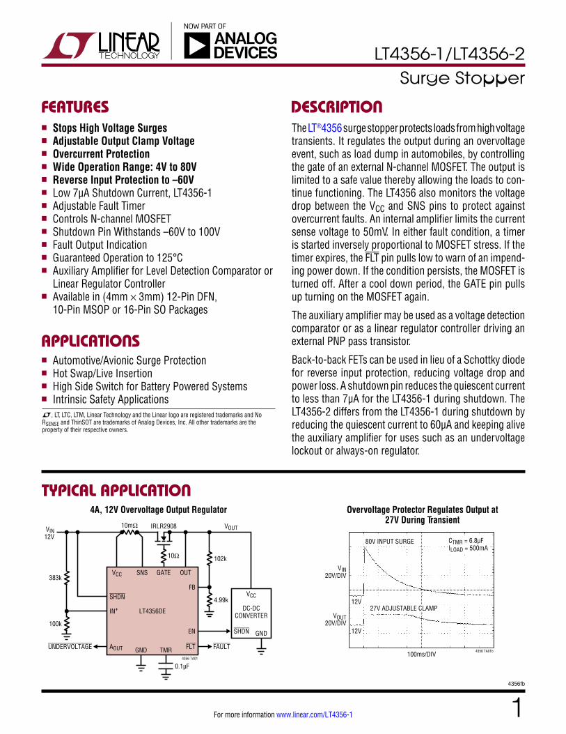
12
11
10
9
8
7
13
1
2
3
4
5
6
IN+
AOUT
GND
EN
FLT
SHDN
TMR
FB
OUT
GATE
SNS
VCC
TOP VIEW
DE PACKAGE12-LEAD (4mm × 3mm) PLASTIC DFN
TJMAX = 125°C, θJA = 43°C/W EXPOSED PAD (PIN 13) PCB GND CONNECTION OPTIONAL
12345
FBOUT
GATESNSVCC
109876
TMRGNDENFLTSHDN
TOP VIEW
MS PACKAGE10-LEAD PLASTIC MSOP
TJMAX = 125°C, θJA = 120°C/W
TOP VIEW
S PACKAGE16-LEAD PLASTIC SO
1
2
3
4
5
6
7
8
16
15
14
13
12
11
10
9
TMR
FB
NC
OUT
GATE
NC
SNS
VCC
IN+
NC
AOUT
NC
GND
EN
FLT
SHDN
TJMAX = 150°C, θJA = 100°C/W
Storage Temperature Range DE12 .................................................. –65°C to 125°C MS, SO .............................................. –65°C to 150°C
Lead Temperature (Soldering, 10 sec) MS, SO ............................................................. 300°C
Absolute MAxiMuM rAtings
pin conFigurAtion
(Notes 1 and 2)
LT4356-1/LT4356-2
34356fb
For more information www.linear.com/LT4356-1
LEAD FREE FINISH TAPE AND REEL PART MARKING* PACKAGE DESCRIPTION TEMPERATURE RANGE
LT4356CDE-1#PBF LT4356CDE-1#TRPBF 43561 12-Lead (4mm × 3mm) Plastic DFN 0°C to 70°C
LT4356IDE-1#PBF LT4356IDE-1#TRPBF 43561 12-Lead (4mm × 3mm) Plastic DFN –40°C to 85°C
LT4356HDE-1#PBF LT4356HDE-1#TRPBF 43561 12-Lead (4mm × 3mm) Plastic DFN –40°C to 125°C
LT4356CDE-2#PBF LT4356CDE-2#TRPBF 43562 12-Lead (4mm × 3mm) Plastic DFN 0°C to 70°C
LT4356IDE-2#PBF LT4356IDE-2#TRPBF 43562 12-Lead (4mm × 3mm) Plastic DFN –40°C to 85°C
LT4356HDE-2#PBF LT4356HDE-2#TRPBF 43562 12-Lead (4mm × 3mm) Plastic DFN –40°C to 125°C
LT4356CMS-1#PBF LT4356CMS-1#TRPBF LTCNS 10-Lead Plastic MSOP 0°C to 70°C
LT4356IMS-1#PBF LT4356IMS-1#TRPBF LTCNS 10-Lead Plastic MSOP –40°C to 85°C
LT4356HMS-1#PBF LT4356HMS-1#TRPBF LTCNS 10-Lead Plastic MSOP –40°C to 125°C
LT4356CS-1#PBF LT4356CS-1#TRPBF LT4356S-1 16-Lead Plastic SO 0°C to 70°C
LT4356IS-1#PBF LT4356IS-1#TRPBF LT4356S-1 16-Lead Plastic SO –40°C to 85°C
LT4356HS-1#PBF LT4356HS-1#TRPBF LT4356S-1 16-Lead Plastic SO –40°C to 125°C
LT4356CS-2#PBF LT4356CS-2#TRPBF LT4356S-2 16-Lead Plastic SO 0°C to 70°C
LT4356IS-2#PBF LT4356IS-2#TRPBF LT4356S-2 16-Lead Plastic SO –40°C to 85°C
LT4356HS-2#PBF LT4356HS-2#TRPBF LT4356S-2 16-Lead Plastic SO –40°C to 125°C
LEAD BASED FINISH TAPE AND REEL PART MARKING* PACKAGE DESCRIPTION TEMPERATURE RANGE
LT4356CDE-1 LT4356CDE-1#TR 43561 12-Lead (4mm × 3mm) Plastic DFN 0°C to 70°C
LT4356IDE-1 LT4356IDE-1#TR 43561 12-Lead (4mm × 3mm) Plastic DFN –40°C to 85°C
LT4356HDE-1 LT4356HDE-1#TR 43561 12-Lead (4mm × 3mm) Plastic DFN –40°C to 125°C
LT4356CDE-2 LT4356CDE-2#TR 43562 12-Lead (4mm × 3mm) Plastic DFN 0°C to 70°C
LT4356IDE-2 LT4356IDE-2#TR 43562 12-Lead (4mm × 3mm) Plastic DFN –40°C to 85°C
LT4356HDE-2 LT4356HDE-2#TR 43562 12-Lead (4mm × 3mm) Plastic DFN –40°C to 125°C
LT4356CMS-1 LT4356CMS-1#TR LTCNS 10-Lead Plastic MSOP 0°C to 70°C
LT4356IMS-1 LT4356IMS-1#TR LTCNS 10-Lead Plastic MSOP –40°C to 85°C
LT4356HMS-1 LT4356HMS-1#TR LTCNS 10-Lead Plastic MSOP –40°C to 125°C
LT4356CS-1 LT4356CS-1#TR LT4356S-1 16-Lead Plastic SO 0°C to 70°C
LT4356IS-1 LT4356CS-1#TR LT4356S-1 16-Lead Plastic SO –40°C to 85°C
LT4356HS-1 LT4356HS-1#TR LT4356S-1 16-Lead Plastic SO –40°C to 125°C
LT4356CS-2 LT4356CS-2#TR LT4356S-2 16-Lead Plastic SO 0°C to 70°C
LT4356IS-2 LT4356IS-2#TR LT4356S-2 16-Lead Plastic SO –40°C to 85°C
LT4356HS-2 LT4356HS-2#TR LT4356S-2 16-Lead Plastic SO –40°C to 125°C
Consult LTC Marketing for parts specified with wider operating temperature ranges. *The temperature grade is identified by a label on the shipping container.For more information on lead free part marking, go to: http://www.linear.com/leadfree/ For more information on tape and reel specifications, go to: http://www.linear.com/tapeandreel/. Some packages are available in 500 unit reels through designated sales channels with #TRMPBF suffix.
orDer inForMAtion http://www.linear.com/product/LT4356-1#orderinfo
LT4356-1/LT4356-2
44356fb
For more information www.linear.com/LT4356-1
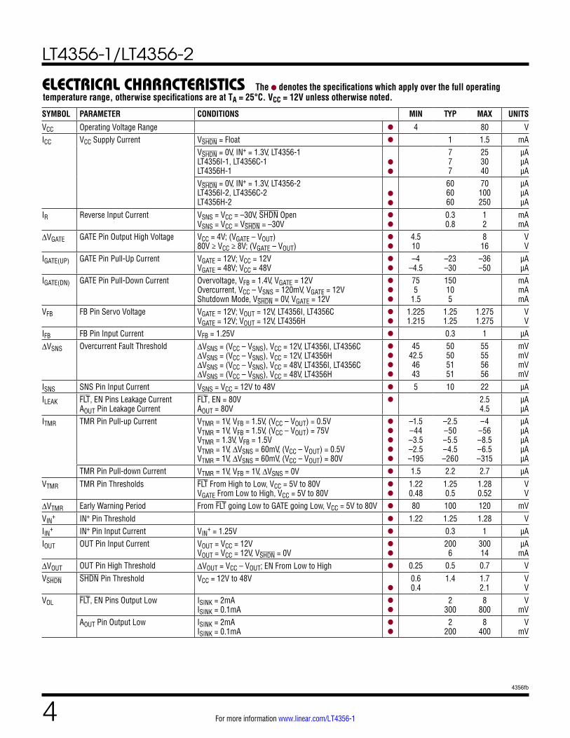
The l denotes the specifications which apply over the full operating temperature range, otherwise specifications are at TA = 25°C. VCC = 12V unless otherwise noted.electricAl chArActeristics
SYMBOL PARAMETER CONDITIONS MIN TYP MAX UNITS
VCC Operating Voltage Range l 4 80 VICC VCC Supply Current VSHDN = Float l 1 1.5 mA
VSHDN = 0V, IN+ = 1.3V, LT4356-1 LT4356I-1, LT4356C-1 LT4356H-1
l
l
7 7 7
25 30 40
µA µA µA
VSHDN = 0V, IN+ = 1.3V, LT4356-2 LT4356I-2, LT4356C-2 LT4356H-2
l
l
60 60 60
70 100 250
µA µA µA
IR Reverse Input Current VSNS = VCC = –30V, SHDN Open VSNS = VCC = VSHDN = –30V
l
l
0.3 0.8
1 2
mA mA
ΔVGATE GATE Pin Output High Voltage VCC = 4V; (VGATE – VOUT) 80V ≥ VCC ≥ 8V; (VGATE – VOUT)
l
l
4.5 10
8 16
V V
IGATE(UP) GATE Pin Pull-Up Current VGATE = 12V; VCC = 12V VGATE = 48V; VCC = 48V
l
l
–4 –4.5
–23 –30
–36 –50
µA µA
IGATE(DN) GATE Pin Pull-Down Current Overvoltage, VFB = 1.4V, VGATE = 12V Overcurrent, VCC – VSNS = 120mV, VGATE = 12V Shutdown Mode, VSHDN = 0V, VGATE = 12V
l
l
l
75 5
1.5
150 10 5
mA mA mA
VFB FB Pin Servo Voltage VGATE = 12V; VOUT = 12V, LT4356I, LT4356C VGATE = 12V; VOUT = 12V, LT4356H
l
l
1.225 1.215
1.25 1.25
1.275 1.275
V V
IFB FB Pin Input Current VFB = 1.25V l 0.3 1 µAΔVSNS Overcurrent Fault Threshold ΔVSNS = (VCC – VSNS), VCC = 12V, LT4356I, LT4356C
ΔVSNS = (VCC – VSNS), VCC = 12V, LT4356H ΔVSNS = (VCC – VSNS), VCC = 48V, LT4356I, LT4356C ΔVSNS = (VCC – VSNS), VCC = 48V, LT4356H
l
l
l
l
45 42.5 46 43
50 50 51 51
55 55 56 56
mV mV mV mV
ISNS SNS Pin Input Current VSNS = VCC = 12V to 48V l 5 10 22 µAILEAK FLT, EN Pins Leakage Current
AOUT Pin Leakage CurrentFLT, EN = 80V AOUT = 80V
l 2.5 4.5
µA µA
ITMR TMR Pin Pull-up Current VTMR = 1V, VFB = 1.5V, (VCC – VOUT) = 0.5V VTMR = 1V, VFB = 1.5V, (VCC – VOUT) = 75V VTMR = 1.3V, VFB = 1.5V VTMR = 1V, ΔVSNS = 60mV, (VCC – VOUT) = 0.5V VTMR = 1V, ΔVSNS = 60mV, (VCC – VOUT) = 80V
l
l
l
l
l
–1.5 –44 –3.5 –2.5 –195
–2.5 –50 –5.5 –4.5 –260
–4 –56 –8.5 –6.5 –315
µA µA µA µA µA
TMR Pin Pull-down Current VTMR = 1V, VFB = 1V, ΔVSNS = 0V l 1.5 2.2 2.7 µAVTMR TMR Pin Thresholds FLT From High to Low, VCC = 5V to 80V
VGATE From Low to High, VCC = 5V to 80Vl
l
1.22 0.48
1.25 0.5
1.28 0.52
V V
ΔVTMR Early Warning Period From FLT going Low to GATE going Low, VCC = 5V to 80V l 80 100 120 mVVIN
+ IN+ Pin Threshold l 1.22 1.25 1.28 VIIN+ IN+ Pin Input Current VIN
+ = 1.25V l 0.3 1 µAIOUT OUT Pin Input Current VOUT = VCC = 12V
VOUT = VCC = 12V, VSHDN = 0Vl
l
200 6
300 14
µA mA
ΔVOUT OUT Pin High Threshold ΔVOUT = VCC – VOUT; EN From Low to High l 0.25 0.5 0.7 VVSHDN SHDN Pin Threshold VCC = 12V to 48V
l
0.6 0.4
1.4 1.7 2.1
V V
VOL FLT, EN Pins Output Low ISINK = 2mA ISINK = 0.1mA
l
l
2 300
8 800
V mV
AOUT Pin Output Low ISINK = 2mA ISINK = 0.1mA
l
l
2 200
8 400
V mV
LT4356-1/LT4356-2
54356fb
For more information www.linear.com/LT4356-1
The l denotes the specifications which apply over the full operating temperature range, otherwise specifications are at TA = 25°C. VCC = 12V unless otherwise noted.
Note 1: Stresses beyond those listed under Absolute Maximum Ratings may cause permanent damage to the device. Exposure to any Absolute Maximum Rating condition for extended periods may affect device reliability and lifetime.Note 2: All currents into device pins are positive; all currents out of device pins are negative. All voltages are referenced to GND unless otherwise specified.
Note 3: An internal clamp limits the GATE pin to a minimum of 10V above the OUT pin. Driving this pin to voltages beyond the clamp may damage the device.
electricAl chArActeristicsSYMBOL PARAMETER CONDITIONS MIN TYP MAX UNITS
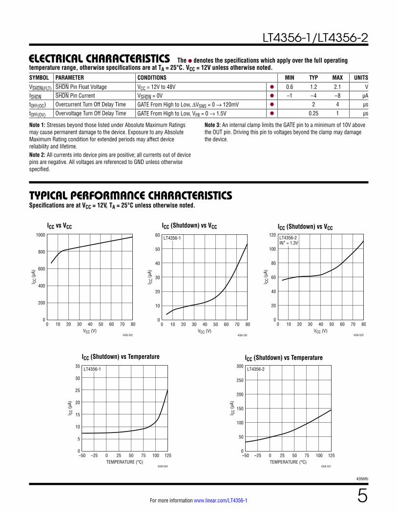
VSHDN(FLT) SHDN Pin Float Voltage VCC = 12V to 48V l 0.6 1.2 2.1 VISHDN SHDN Pin Current VSHDN = 0V l –1 –4 –8 µAtOFF(OC) Overcurrent Turn Off Delay Time GATE From High to Low, ΔVSNS = 0 → 120mV l 2 4 µstOFF(OV) Overvoltage Turn Off Delay Time GATE From High to Low, VFB = 0 → 1.5V l 0.25 1 µs
typicAl perForMAnce chArActeristics
ICC (Shutdown) vs VCC
ICC vs VCC
VCC (V)0
0
I CC
(µA)
10
20
30
40
20 40 60 80
4356 G01
50
60
10 30 50 70
LT4356-1
VCC (V)0
0
I CC
(µA)
200
400
600
20 40 60 80
4356 G02
800
1000
10 30 50 70
Specifications are at VCC = 12V, TA = 25°C unless otherwise noted.
ICC (Shutdown) vs VCC
VCC (V)0
0
I CC
(µA)
20
40
20 40 60 80
4356 G20
120LT4356-2IN+ = 1.3V
60
80
100
10 30 50 70
TEMPERATURE (°C)–500
I CC
(µA)
50
100
150
200
0 50 100 125
4356 G21
250
300
–25 25 75
LT4356-2
ICC (Shutdown) vs Temperature
ICC (Shutdown) vs Temperature
TEMPERATURE (°C)–500
I CC
(µA)
5
10
15
20
0 50 100 125
4356 G03
25
35
30
–25 25 75
LT4356-1
LT4356-1/LT4356-2
64356fb
For more information www.linear.com/LT4356-1
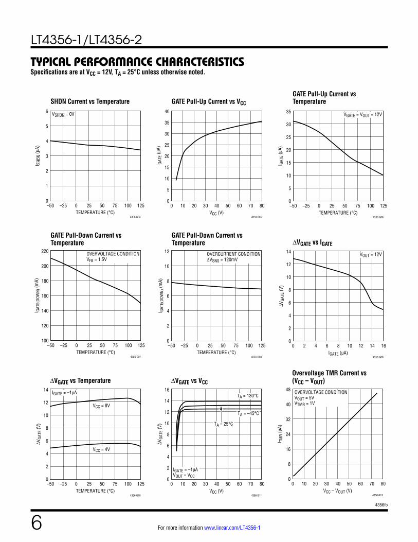
SHDN Current vs Temperature
GATE Pull-Up Current vs VCC
GATE Pull-Up Current vs Temperature
GATE Pull-Down Current vs Temperature
GATE Pull-Down Current vs Temperature
ΔVGATE vs IGATE
TEMPERATURE (°C)–500
I SHD
N (µ
A)
1
2
3
0 50 100 125
4356 G04
4
6
5
–25 25 75
VSHDN = 0V
VCC (V)0
0
I GAT
E (µ
A)
10
20
30
5
15
25
35
20 40 60 80
4356 G05
40
10 30 50 70TEMPERATURE (°C)
–500
I GAT
E (µ
A)
5
10
15
20
0 50 100 125
4356 G06
25
35
30
–25 25 75
VGATE = VOUT = 12V
TEMPERATURE (°C)–50
100
I GAT
E(DO
WN)
(mA)
120
140
160
0 50 100 125
4356 G07
180
220
200
–25 25 75
OVERVOLTAGE CONDITIONVFB = 1.5V
TEMPERATURE (°C)–500
I GAT
E(DO
WN)
(mA)
2
4
6
0 50 100 125
4356 G08
8
12
10
–25 25 75
OVERCURRENT CONDITION∆VSNS = 120mV
IGATE (µA)0
0
∆VGA
TE (V
)
4
2
6
8
10
4 8 12 16
4356 G09
12
14
2 6 10 14
VOUT = 12V
typicAl perForMAnce chArActeristicsSpecifications are at VCC = 12V, TA = 25°C unless otherwise noted.
ΔVGATE vs Temperature
ΔVGATE vs VCC
Overvoltage TMR Current vs (VCC – VOUT)
TEMPERATURE (°C)–50 0 50 100 125–25 25 750
∆VGA
TE (V
)
4
2
6
8
10
4356 G10
12
14 IGATE = –1µA
VCC = 8V
VCC = 4V
VCC (V)0 20 40 60 80
4356 G11
10 30 50 700
∆VGA
TE (V
)
4
2
6
8
10
12
16
14
IGATE = –1µAVOUT = VCC
TA = –45°C
TA = 25°C
TA = 130°C
VCC – VOUT (V)0
0
I TM
R (µ
A)
8
16
24
32
20 40 60 80
4356 G12
40
48
10 30 50 70
OVERVOLTAGE CONDITIONVOUT = 5VVTMR = 1V
LT4356-1/LT4356-2
74356fb
For more information www.linear.com/LT4356-1
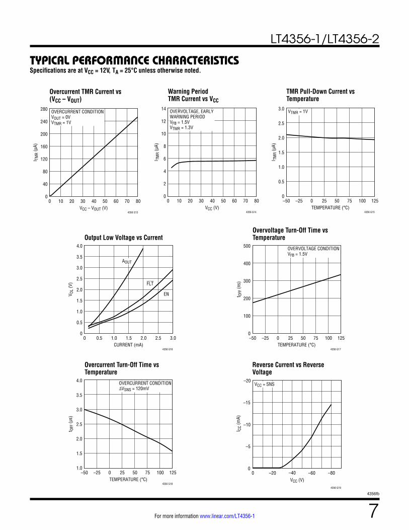
Overcurrent TMR Current vs (VCC – VOUT)
Warning Period TMR Current vs VCC
TMR Pull-Down Current vs Temperature
Output Low Voltage vs Current
Overvoltage Turn-Off Time vs Temperature
Overcurrent Turn-Off Time vs Temperature
VCC – VOUT (V)0
0
I TM
R (µ
A)
40
80
120
160
20 40 60 80
4356 G13
200
280
240
10 30 50 70
OVERCURRENT CONDITIONVOUT = 0VVTMR = 1V
VCC (V)0 20 40 60 80
4356 G14
10 30 50 700
I TM
R (µ
A)
4
2
6
8
10
12
14 OVERVOLTAGE, EARLYWARNING PERIODVFB = 1.5VVTMR = 1.3V
TEMPERATURE (°C)–500
I TM
R (µ
A)
0 50 100 125
4356 G15
3.0
2.5
2.0
1.5
1.0
0.5
–25 25 75
VTMR = 1V
CURRENT (mA)0
0
V OL
(V)
1.0
2.0
3.0
0.5
1.5
2.5
3.5
2.0 3.0
4356 G16
4.0
1.00.5 2.51.5
AOUT
EN
FLT
TEMPERATURE (°C)–500
100
t OFF
(ns)
0 50 100 125
4356 G17
500
400
300
200
–25 25 75
OVERVOLTAGE CONDITIONVFB = 1.5V
TEMPERATURE (°C)–50
1.0
1.5
t OFF
(µs)
0 50 100 125
4356 G18
4.0
3.5
3.0
2.5
2.0
–25 25 75
OVERCURRENT CONDITION∆VSNS = 120mV
typicAl perForMAnce chArActeristicsSpecifications are at VCC = 12V, TA = 25°C unless otherwise noted.
VCC (V)0
I CC
(mA)
–10
–15
–80
4356 G19
–5
0–20 –40 –60
–20VCC = SNS
Reverse Current vs Reverse Voltage
LT4356-1/LT4356-2
84356fb
For more information www.linear.com/LT4356-1
pin FunctionsAOUT (DFN and SO Packages Only): Amplifier Output. Open collector output of the auxiliary amplifier. It is capable of sinking up to 2mA from 80V. The negative input of the amplifier is internally connected to a 1.25V reference.
EN: Open-Collector Enable Output. The EN pin goes high impedance when the voltage at the OUT pin is above (VCC – 0.7V), indicating the external MOSFET is fully on. The state of the pin is latched until the OUT pin voltage resets at below 0.5V and goes back up above 2V. The internal NPN is capable of sinking up to 3mA of current from 80V to drive an LED or opto-coupler.
Exposed Pad (DFN Package Only): Exposed pad may be left open or connected to device ground (GND).
FB: Voltage Regulator Feedback Input. Connect this pin to the center tap of the output resistive divider connected between the OUT pin and ground. During an overvoltage condition, the GATE pin is servoed to maintain a 1.25V threshold at the FB pin. This pin is clamped internally to 7V. Tie to GND to disable the OV clamp.
FLT: Open-Collector Fault Output. This pin pulls low after the voltage at the TMR pin has reached the fault threshold of 1.25V. It indicates the pass transistor is about to turn off because either the supply voltage has stayed at an elevated level for an extended period of time (voltage fault) or the device is in an overcurrent condition (current fault). The internal NPN is capable of sinking up to 3mA of current from 80V to drive an LED or opto-coupler.
GATE: N-Channel MOSFET Gate Drive Output. The GATE pin is pulled up by an internal charge pump current source and clamped to 14V above the OUT pin. Both voltage and cur-rent amplifiers control the GATE pin to regulate the output voltage and limit the current through the MOSFET.
GND: Device Ground.
IN+ (DFN and SO Packages Only): Positive Input of the Auxiliary Amplifier. This amplifier can be used as a level detection comparator with external hysteresis or linear regulator controlling an external PNP transistor. This pin is clamped internally to 7V. Connect to ground if unused.
OUT: Output Voltage Sense Input. This pin senses the voltage at the source of the N-channel MOSFET and sets the fault timer current. When the OUT pin voltage reaches 0.7V away from VCC, the EN pin goes high impedance.
SHDN: Shutdown Control Input. The LT4356 can be shut down to a low current mode by pulling the SHDN pin below 0.4V. Pull this pin above 2.1V or disconnect it and allow the internal current source to turn the part back on. The leakage current to ground at the pin should be limited to no more than 1µA if no pull up device is used to turn the part on. The SHDN pin can be pulled up to 100V or below GND by 60V without damage. In shutdown, the auxiliary amplifier turns off in the LT4356-1 but continues operating in the LT4356-2.
SNS: Current Sense Input. Connect this pin to the output of the current sense resistor. The current limit circuit controls the GATE pin to limit the sense voltage between VCC and SNS pins to 50mV. At the same time the sense amplifier also starts a current source to charge up the TMR pin. This pin can be pulled below GND by up to 60V, though the voltage difference with the VCC pin must be limited to less than 30V. Connect to VCC if unused.
TMR: Fault Timer Input. Connect a capacitor between this pin and ground to set the times for early warning, fault and cool down periods. The current charging up this pin during fault conditions depends on the voltage difference between the VCC and OUT pins. When VTMR reaches 1.25V, the FLT pin pulls low to indicate the detection of a fault condition. If the condition persists, the pass transistor turns off when VTMR reaches the threshold of 1.35V. As soon as the fault condition disappears, the pull up current stops and a 2µA current starts to pull the TMR pin down. When VTMR reaches the retry threshold of 0.5V, the GATE pin pulls high turning back on the pass transistor. A minimum of 10nF capacitor is needed to compensate the loop. A 10V rated X7R capacitor is recommended for CTMR.
VCC: Positive Supply Voltage Input. The positive supply input ranges from 4V to 80V for normal operation. It can also be pulled below ground potential by up to 60V during a reverse battery condition, without damaging the part. The supply current is reduced to 7µA with all the functional blocks off.
LT4356-1/LT4356-2
94356fb
For more information www.linear.com/LT4356-1
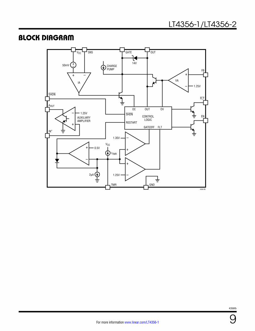
block DiAgrAM
–
+
+ –
+
–
+–
VCC
SHDN
IN+
AUXILIARYAMPLIFIER
IA
1.25V
50mV
2µA
1.35V
1.25V –
+
1.25V
0.5V
SNS
TMR GND
GATE
14V
AOUT
OUT
4356 BD
VCC
ITMR
FLT
EN
FB+
–
CHARGEPUMP
CONTROLLOGIC
GATEOFF FLT
OUT OVOC
VA
SHDN
RESTART
+
–
LT4356-1/LT4356-2
104356fb
For more information www.linear.com/LT4356-1
Some power systems must cope with high voltage surges of short duration such as those in automobiles. Load circuitry must be protected from these transients, yet high availability systems must continue operating during these events.
The LT4356 is an overvoltage protection regulator that drives an external N-channel MOSFET as the pass transis-tor. It operates from a wide supply voltage range of 4V to 80V. It can also be pulled below ground potential by up to 60V without damage. The low power supply require-ment of 4V allows it to operate even during cold cranking conditions in automotive applications. The internal charge pump turns on the N-channel MOSFET to supply current to the loads with very little power loss. Two MOSFETs can be connected back to back to replace an inline Schottky diode for reverse input protection. This improves the ef-ficiency and increases the available supply voltage level to the load circuitry during cold crank.
Normally, the pass transistor is fully on, powering the loads with very little voltage drop. When the supply volt-age surges too high, the voltage amplifier (VA) controls the gate of the MOSFET and regulates the voltage at the source pin to a level that is set by the external resistive divider from the OUT pin to ground and the internal 1.25V reference. A current source starts charging up the capaci-tor connected at the TMR pin to ground. If the voltage at the TMR pin, VTMR, reaches 1.25V, the FLT pin pulls low to indicate impending turn-off due to the overvoltage condition. The pass transistor stays on until the TMR pin reaches 1.35V, at which point the GATE pin pulls low turning off the MOSFET.
The potential at the TMR pin starts decreasing as soon as the overvoltage condition disappears. When the voltage at the TMR pin reaches 0.5V the GATE pin begins rising, turning on the MOSFET. The FLT pin will then go to a high impedance state.
The fault timer allows the load to continue functioning during short transient events while protecting the MOSFET from being damaged by a long period of supply overvolt-age, such as a load dump in automobiles. The timer period varies with the voltage across the MOSFET. A higher voltage corresponds to a shorter fault timer period, ensuring the MOSFET operates within its safe operating area (SOA).
The LT4356 senses an overcurrent condition by monitor-ing the voltage across an optional sense resistor placed between the VCC and SNS pins. An active current limit circuit (IA) controls the GATE pin to limit the sense volt-age to 50mV. A current is also generated to start charging up the TMR pin. This current is about 5 times the current generated during an overvoltage event. The FLT pin pulls low when the voltage at the TMR pin reaches 1.25V and the MOSFET is turned off when it reaches 1.35V.
An auxiliary amplifier is provided with the negative input connected to an internal 1.25V reference. The output pull down device is capable of sinking up to 2mA of current allowing it to drive an LED or opto coupler. This amplifier can be configured as a linear regulator controller driving an external PNP transistor or a comparator function to monitor voltages.
A shutdown pin turns off the pass transistor and reduces the supply current to less than 7µA for the LT4356-1. The supply current drops down to 60µA while keeping the internal reference and the auxiliary amplifier active for the LT4356-2 version during shutdown.
operAtion
LT4356-1/LT4356-2
114356fb
For more information www.linear.com/LT4356-1
The LT4356 can limit the voltage and current to the load circuitry during supply transients or overcurrent events. The total fault timer period should be set to ride through short overvoltage transients while not causing damage to the pass transistor. The selection of this N-channel MOSFET pass transistor is critical for this application. It must stay on and provide a low impedance path from the input supply to the load during normal operation and then dissipate power during overvoltage or overcurrent conditions.
The following sections describe the overcurrent and the overvoltage faults, and the selection of the timer capacitor value based on the required warning time. The selection of the N-channel MOSFET pass transistor is discussed next. Auxiliary amplifier, reverse input, and the shutdown functions are covered after the MOSFET selection. External component selection is discussed in detail in the Design Example section.
Overvoltage Fault
The LTC4356 limits the voltage at the OUT pin during an overvoltage situation. An internal voltage amplifier regu-lates the GATE pin voltage to maintain a 1.25V threshold at the FB pin. During this period of time, the power MOSFET is still on and continues to supply current to the load. This allows uninterrupted operation during short overvoltage transient events.
When the voltage regulation loop is engaged for longer than the time-out period, set by the timer capacitor con-nected from the TMR pin to ground, an overvoltage fault is detected. The GATE pin is pulled down to the OUT pin by a 150mA current. After the fault condition has disappeared and a cool down period has transpired, the GATE pin starts to pull high again. This prevents the power MOSFET from being damaged during a long period of overvoltage, such as during load dump in automobiles.
Overcurrent Fault
The LT4356 features an adjustable current limit that protects against short circuits or excessive load current. During an overcurrent event, the GATE pin is regulated to limit the current sense voltage across the VCC and SNS pins to 50mV.
An overcurrent fault occurs when the current limit circuitry has been engaged for longer than the time-out delay set by the timer capacitor. The GATE pin is then immediately pulled low by a 10mA current to GND turning off the MOSFET. After the fault condition has disappeared and a cool down period has transpired, the GATE pin is allowed to pull back up and turn on the pass transistor.
Fault Timer
The LT4356 includes an adjustable fault timer pin. Con-necting a capacitor from the TMR pin to ground sets the delay timer period before the MOSFET is turned off. The same capacitor also sets the cool down period before the MOSFET is allowed to turn back on after the fault condition has disappeared.
Once a fault condition, either overvoltage or overcurrent, is detected, a current source charges up the TMR pin. The current level varies depending on the voltage drop across the drain and source terminals of the power MOSFET(VDS), which is typically from the VCC pin to the OUT pin. This scheme takes better advantage of the available Safe Operating Area (SOA) of the MOSFET than would a fixed timer current. The timer function operates down to VCC = 5V across the whole temperature range.
ApplicAtions inForMAtion
LT4356-1/LT4356-2
124356fb
For more information www.linear.com/LT4356-1
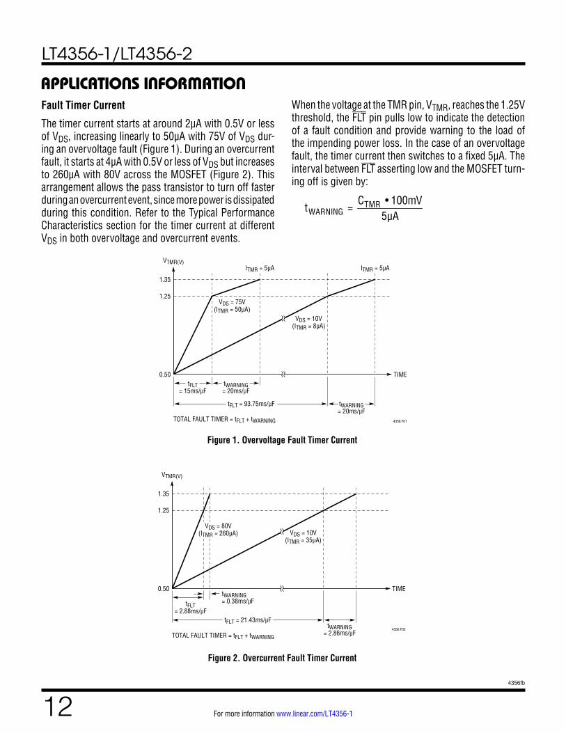
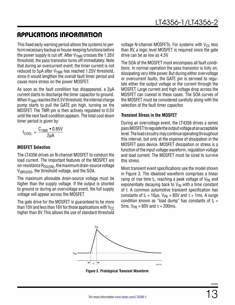
Fault Timer Current
The timer current starts at around 2µA with 0.5V or less of VDS, increasing linearly to 50µA with 75V of VDS dur-ing an overvoltage fault (Figure 1). During an overcurrent fault, it starts at 4µA with 0.5V or less of VDS but increases to 260µA with 80V across the MOSFET (Figure 2). This arrangement allows the pass transistor to turn off faster during an overcurrent event, since more power is dissipated during this condition. Refer to the Typical Performance Characteristics section for the timer current at different VDS in both overvoltage and overcurrent events.
When the voltage at the TMR pin, VTMR, reaches the 1.25V threshold, the FLT pin pulls low to indicate the detection of a fault condition and provide warning to the load of the impending power loss. In the case of an overvoltage fault, the timer current then switches to a fixed 5µA. The interval between FLT asserting low and the MOSFET turn-ing off is given by:
tWARNING =
CTMR • 100mV5µA
ApplicAtions inForMAtion
Figure 1. Overvoltage Fault Timer Current
Figure 2. Overcurrent Fault Timer Current
tFLT= 15ms/µF
TOTAL FAULT TIMER = tFLT + tWARNING
tWARNING= 20ms/µF
tFLT = 93.75ms/µF tWARNING= 20ms/µF
VTMR(V)ITMR = 5µA ITMR = 5µA
VDS = 75V(ITMR = 50µA)
VDS = 10V(ITMR = 8µA)
1.35
1.25
TIME
4356 F01
0.50
tFLT= 2.88ms/µF
TOTAL FAULT TIMER = tFLT + tWARNING
tFLT = 21.43ms/µFtWARNING
= 2.86ms/µF
tWARNING = 0.38ms/µF
VTMR(V)
VDS = 10V(ITMR = 35µA)
1.35
1.25
0.50 TIME
4356 F02
VDS = 80V(ITMR = 260µA)
LT4356-1/LT4356-2
134356fb
For more information www.linear.com/LT4356-1
voltage N-channel MOSFETs. For systems with VCC less than 8V, a logic level MOSFET is required since the gate drive can be as low as 4.5V.
The SOA of the MOSFET must encompass all fault condi-tions. In normal operation the pass transistor is fully on, dissipating very little power. But during either overvoltage or overcurrent faults, the GATE pin is servoed to regu-late either the output voltage or the current through the MOSFET. Large current and high voltage drop across the MOSFET can coexist in these cases. The SOA curves of the MOSFET must be considered carefully along with the selection of the fault timer capacitor.
Transient Stress in the MOSFET
During an overvoltage event, the LT4356 drives a series pass MOSFET to regulate the output voltage at an acceptable level. The load circuitry may continue operating throughout this interval, but only at the expense of dissipation in the MOSFET pass device. MOSFET dissipation or stress is a function of the input voltage waveform, regulation voltage and load current. The MOSFET must be sized to survive this stress.
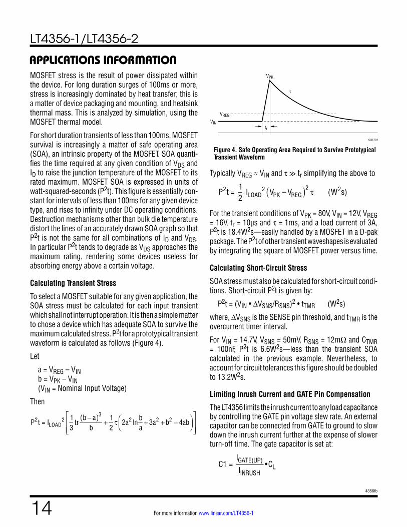
Most transient event specifications use the model shown in Figure 3. The idealized waveform comprises a linear ramp of rise time tr, reaching a peak voltage of VPK and exponentially decaying back to VIN with a time constant of t. A common automotive transient specification has constants of tr = 10µs, VPK = 80V and t = 1ms. A surge condition known as “load dump” has constants of tr = 5ms, VPK = 60V and t = 200ms.
This fixed early warning period allows the systems to per-form necessary backup or house-keeping functions before the power supply is cut off. After VTMR crosses the 1.35V threshold, the pass transistor turns off immediately. Note that during an overcurrent event, the timer current is not reduced to 5µA after VTMR has reached 1.25V threshold, since it would lengthen the overall fault timer period and cause more stress on the power MOSFET.
As soon as the fault condition has disappeared, a 2µA current starts to discharge the timer capacitor to ground. When VTMR reaches the 0.5V threshold, the internal charge pump starts to pull the GATE pin high, turning on the MOSFET. The TMR pin is then actively regulated to 0.5V until the next fault condition appears. The total cool down timer period is given by:
tCOOL =
CTMR • 0.85V2µA
MOSFET Selection
The LT4356 drives an N-channel MOSFET to conduct the load current. The important features of the MOSFET are on-resistance RDS(ON), the maximum drain-source voltage V(BR)DSS, the threshold voltage, and the SOA.
The maximum allowable drain-source voltage must be higher than the supply voltage. If the output is shorted to ground or during an overvoltage event, the full supply voltage will appear across the MOSFET.
The gate drive for the MOSFET is guaranteed to be more than 10V and less than 16V for those applications with VCC higher than 8V. This allows the use of standard threshold
ApplicAtions inForMAtion
Figure 3. Prototypical Transient Waveform
VPK
τ
VIN
4356 F03tr
LT4356-1/LT4356-2
144356fb
For more information www.linear.com/LT4356-1
ApplicAtions inForMAtionMOSFET stress is the result of power dissipated within the device. For long duration surges of 100ms or more, stress is increasingly dominated by heat transfer; this is a matter of device packaging and mounting, and heatsink thermal mass. This is analyzed by simulation, using the MOSFET thermal model.
For short duration transients of less than 100ms, MOSFET survival is increasingly a matter of safe operating area (SOA), an intrinsic property of the MOSFET. SOA quanti-fies the time required at any given condition of VDS and ID to raise the junction temperature of the MOSFET to its rated maximum. MOSFET SOA is expressed in units of watt-squared-seconds (P2t). This figure is essentially con-stant for intervals of less than 100ms for any given device type, and rises to infinity under DC operating conditions. Destruction mechanisms other than bulk die temperature distort the lines of an accurately drawn SOA graph so that P2t is not the same for all combinations of ID and VDS. In particular P2t tends to degrade as VDS approaches the maximum rating, rendering some devices useless for absorbing energy above a certain voltage.
Calculating Transient Stress
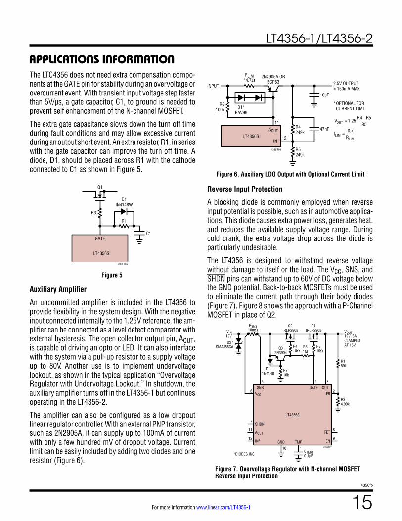
To select a MOSFET suitable for any given application, the SOA stress must be calculated for each input transient which shall not interrupt operation. It is then a simple matter to chose a device which has adequate SOA to survive the maximum calculated stress. P2t for a prototypical transient waveform is calculated as follows (Figure 4).
Let
a = VREG – VIN b = VPK – VIN (VIN = Nominal Input Voltage)
Then
P2t = ILOAD
2 13
trb − a( )3
b+ 1
2t 2a2 ln
ba
+ 3a2 + b2 − 4ab
Typically VREG ≈ VIN and t >> tr simplifying the above to
P2t =
12
ILOAD2 VPK – VREG( )2 t (W2s)
For the transient conditions of VPK = 80V, VIN = 12V, VREG = 16V, tr = 10µs and t = 1ms, and a load current of 3A, P2t is 18.4W2s—easily handled by a MOSFET in a D-pak package. The P2t of other transient waveshapes is evaluated by integrating the square of MOSFET power versus time.
Calculating Short-Circuit Stress
SOA stress must also be calculated for short-circuit condi-tions. Short-circuit P2t is given by:
P2t = (VIN • ΔVSNS/RSNS)2 • tTMR (W2s)
where, ΔVSNS is the SENSE pin threshold, and tTMR is the overcurrent timer interval.
For VIN = 14.7V, VSNS = 50mV, RSNS = 12mΩ and CTMR = 100nF, P2t is 6.6W2s—less than the transient SOA calculated in the previous example. Nevertheless, to account for circuit tolerances this figure should be doubled to 13.2W2s.
Limiting Inrush Current and GATE Pin Compensation
The LT4356 limits the inrush current to any load capacitance by controlling the GATE pin voltage slew rate. An external capacitor can be connected from GATE to ground to slow down the inrush current further at the expense of slower turn-off time. The gate capacitor is set at:
C1 =
I
IGATE(UP)
INRUSH•CL
Figure 4. Safe Operating Area Required to Survive Prototypical Transient Waveform
VPK
τ
VIN
4356 F04
VREG
tr
LT4356-1/LT4356-2
154356fb
For more information www.linear.com/LT4356-1
Figure 5
Figure 6. Auxiliary LDO Output with Optional Current Limit
C1
R3
4356 F05
LT4356S
GATE
Q1
R1
D1IN4148W
RLIM*4.7Ω
D1*BAV99
2N2905A ORBCP53
INPUT 2.5V OUTPUT≈ 150mA MAX
* OPTIONAL FOR CURRENT LIMIT
LT4356SAOUT
IN+
11
12
R6100k
4356 F06
R4249k
47nF
R5249k
10µF
VOUT = 1.25R4 +R5
R5
ILIM ≈0.7
RLIM
ApplicAtions inForMAtionThe LTC4356 does not need extra compensation compo-nents at the GATE pin for stability during an overvoltage or overcurrent event. With transient input voltage step faster than 5V/µs, a gate capacitor, C1, to ground is needed to prevent self enhancement of the N-channel MOSFET.
The extra gate capacitance slows down the turn off time during fault conditions and may allow excessive current during an output short event. An extra resistor, R1, in series with the gate capacitor can improve the turn off time. A diode, D1, should be placed across R1 with the cathode connected to C1 as shown in Figure 5.
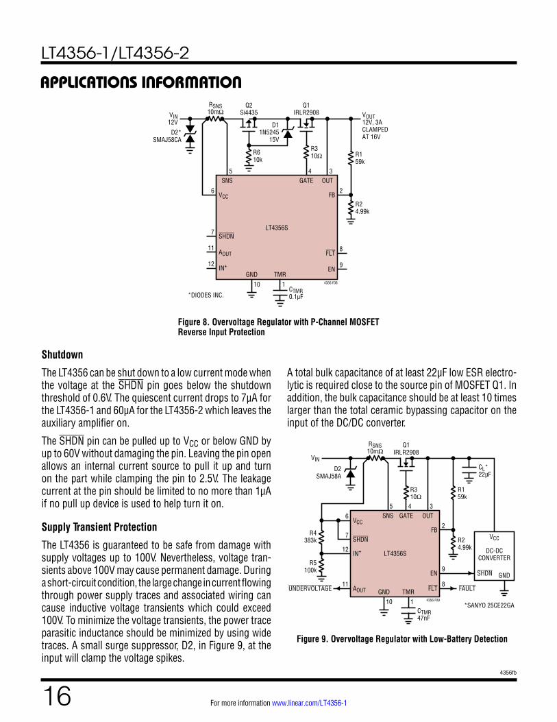
Reverse Input Protection
A blocking diode is commonly employed when reverse input potential is possible, such as in automotive applica-tions. This diode causes extra power loss, generates heat, and reduces the available supply voltage range. During cold crank, the extra voltage drop across the diode is particularly undesirable.
The LT4356 is designed to withstand reverse voltage without damage to itself or the load. The VCC, SNS, and SHDN pins can withstand up to 60V of DC voltage below the GND potential. Back-to-back MOSFETs must be used to eliminate the current path through their body diodes (Figure 7). Figure 8 shows the approach with a P-Channel MOSFET in place of Q2.
Figure 7. Overvoltage Regulator with N-channel MOSFET Reverse Input Protection
CTMR0.1µF
RSNS10mΩ
Q1IRLR2908
Q2IRLR2908VIN
12VVOUT12V, 3ACLAMPEDAT 16V
4356 F07
LT4356S
GND TMR10 1
OUTSNS35
SHDN7
AOUT11
IN+12
VCC6
EN
FLT
FB
9
8
2
D2*SMAJ58CA
R24.99k
R159k
GATE4
R710k
R51M
Q32N3904
D11N4148
R310Ω
R410Ω
*DIODES INC.
Auxiliary Amplifier
An uncommitted amplifier is included in the LT4356 to provide flexibility in the system design. With the negative input connected internally to the 1.25V reference, the am-plifier can be connected as a level detect comparator with external hysteresis. The open collector output pin, AOUT, is capable of driving an opto or LED. It can also interface with the system via a pull-up resistor to a supply voltage up to 80V. Another use is to implement undervoltage lockout, as shown in the typical application “Overvoltage Regulator with Undervoltage Lockout.” In shutdown, the auxiliary amplifier turns off in the LT4356-1 but continues operating in the LT4356-2.
The amplifier can also be configured as a low dropout linear regulator controller. With an external PNP transistor, such as 2N2905A, it can supply up to 100mA of current with only a few hundred mV of dropout voltage. Current limit can be easily included by adding two diodes and one resistor (Figure 6).
LT4356-1/LT4356-2
164356fb
For more information www.linear.com/LT4356-1
ApplicAtions inForMAtion
Shutdown
The LT4356 can be shut down to a low current mode when the voltage at the SHDN pin goes below the shutdown threshold of 0.6V. The quiescent current drops to 7µA for the LT4356-1 and 60µA for the LT4356-2 which leaves the auxiliary amplifier on.
The SHDN pin can be pulled up to VCC or below GND by up to 60V without damaging the pin. Leaving the pin open allows an internal current source to pull it up and turn on the part while clamping the pin to 2.5V. The leakage current at the pin should be limited to no more than 1µA if no pull up device is used to help turn it on.
Supply Transient Protection
The LT4356 is guaranteed to be safe from damage with supply voltages up to 100V. Nevertheless, voltage tran-sients above 100V may cause permanent damage. During a short-circuit condition, the large change in current flowing through power supply traces and associated wiring can cause inductive voltage transients which could exceed 100V. To minimize the voltage transients, the power trace parasitic inductance should be minimized by using wide traces. A small surge suppressor, D2, in Figure 9, at the input will clamp the voltage spikes.
A total bulk capacitance of at least 22µF low ESR electro-lytic is required close to the source pin of MOSFET Q1. In addition, the bulk capacitance should be at least 10 times larger than the total ceramic bypassing capacitor on the input of the DC/DC converter.
Figure 8. Overvoltage Regulator with P-Channel MOSFET Reverse Input Protection
Figure 9. Overvoltage Regulator with Low-Battery Detection
CTMR0.1µF
RSNS10mΩ
Q1IRLR2908
Q2Si4435VIN
12VVOUT12V, 3ACLAMPEDAT 16V
4356 F08
LT4356S
GND TMR10 1
OUTSNS35
SHDN7
AOUT11
IN+12
VCC6
EN
FLT
FB
9
8
2
R24.99k
R159k
GATE4
R610k
D11N5245
15VR310Ω
D2*SMAJ58CA
*DIODES INC.
CTMR47nF
*SANYO 25CE22GA
R310Ω
RSNS10mΩ
Q1IRLR2908
D2SMAJ58A
VIN
4356 F09
LT4356S
GND TMR
OUTGATESNS
IN+
SHDN
AOUT FAULT
EN
FLTUNDERVOLTAGE
FB
CL*22µF
DC-DCCONVERTER
GNDSHDN
VCCR24.99k
R4383k
R5100k
R159k
10 1
345
7
12
VCC6
11
2
9
8
LT4356-1/LT4356-2
174356fb
For more information www.linear.com/LT4356-1
Layout Considerations
To achieve accurate current sensing, Kelvin connection to the current sense resistor (RSNS in Figure 9) is recom-mended. The minimum trace width for 1oz copper foil is 0.02" per amp to ensure the trace stays at a reasonable temperature. 0.03" per amp or wider is recommended. Note that 1oz copper exhibits a sheet resistance of about 530µΩ/square. Small resistances can cause large errors in high current applications. Noise immunity will be improved significantly by locating resistive dividers close to the pins with short VCC and GND traces.
Design Example
As a design example, take an application with the follow-ing specifications: VCC = 8V to 14V DC with transient up to 80V, VOUT ≤ 16V, current limit (ILIM) at 5A, low battery detection at 6V, and 1ms of overvoltage early warning (Figure 9).
First, calculate the resistive divider value to limit VOUT to 16V during an overvoltage event:
VREG =
1.25V • R1 + R2( )R2
= 16V
Set the current through R1 and R2 during the overvoltage condition to 250µA.
R2 =
1.25V250µA
= 5k
Choose 4.99k for R2.
R1 =
16V – 1.25V( ) • R21.25V
= 58.88k
The closest standard value for R1 is 59k.
Next calculate the sense resistor, RSNS, value:
RSNS =
50mVILIM
= 50mV
5A = 10mΩ
CTMR is then chosen for 1ms of early warning time:
CTMR =
1ms • 5µA100mV
= 50nF
The closest standard value for CTMR is 47nF.
Finally, calculate R4 and R5 for the 6V low battery threshold detection:
6V =
1.25V • R4 + R5( )R5
Choose 100k for R5.
R4 =
6V – 1.25V( ) • R51.25V
= 380k
Select 383k for R4.
The pass transistor, Q1, should be chosen to withstand the output short condition with VCC = 14V.
The total overcurrent fault time is:
tOC =
47nF • 0.85V45.5µA
= 0.878ms
The power dissipation on Q1 equals to:
P =
14V • 50mV10mΩ
= 70W
These conditions are well within the Safe Operating Area of IRLR2908.
ApplicAtions inForMAtion
LT4356-1/LT4356-2
184356fb
For more information www.linear.com/LT4356-1
Wide Input Range 5V to 28V Hot Swap with Undervoltage Lockout
CTMR1µF
R310Ω
RSNS20mΩ
Q1SUD50N03-10
VIN
4356 TA02
LT4356DE-1
GND TMR
OUTGATESNS
IN+
SHDN
AOUT
VOUT
EN
FLT
FB
VCC
R749.9k
R6118k
100µF
C147nF
typicAl ApplicAtions
24V Overvoltage Regulator Withstands 150V at VIN
CTMR0.1µF
Q1IRF640VIN
24VVOUTCLAMPED AT 32V
4356 TA03
LT4356DE
GND TMR10 1
OUTSNS35
SHDN7
FLT8
EN9
VCC6
FB2
D2*SMAT70A
R24.99k
R1118k
GATE4
R310Ω
R91k1W
*DIODES INC.
LT4356-1/LT4356-2
194356fb
For more information www.linear.com/LT4356-1
typicAl ApplicAtionsOvervoltage Regulator with Undervoltage Lockout
CTMR0.1µF
R310Ω
RSNS20mΩ
Q1IRLR2908
VIN
4356 TA04
LT4356DE-2
GND TMR
OUTGATESNS
IN+
SHDN
AOUT
VOUTCLAMPED AT 16V
EN
FLT
FB
VCC
R24.99k
R7100k
R6280k
R41M
R51M
R159k
D2*SMAJ58A
UV RISING = 5.04V
*DIODES INC.
Overvoltage Regulator with Low Battery Detection and Output Keep Alive During Shutdown
R310Ω
RSNS10mΩ
VIN12V
VOUT12V, 4ACLAMPED AT 16V
4356 TA05
LT4356DE
GND TMR10 1
OUTGATESNS345
IN+12
SHDN7
VCC
VDD
6
EN
FLT
FB
9
AOUT LBO11
8
2
D11N4746A18V1W
R224.9k
R647k
R4402k
R5105k
R1294k
1k0.5W
Q1IRLR2908
Q2VN2222
CTMR0.1µF
D2*SMAJ58A
*DIODES INC.
LT4356-1/LT4356-2
204356fb
For more information www.linear.com/LT4356-1
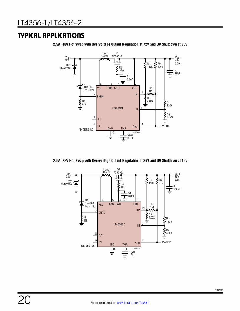
typicAl ApplicAtions2.5A, 48V Hot Swap with Overvoltage Output Regulation at 72V and UV Shutdown at 35V
D11N4714BV = 33V
C16.8nF
CTMR0.1µF
R310Ω
RSNS15mΩ VOUT
48V2.5A
4356 TA06
LT4356DE
GND TMR10 1
OUTGATESNSVCC
3456
SHDN
EN
FLT
7
9
8
AOUT PWRGD
FB
IN+
11
2
12
R71M
CL300µF
R54.02k
R4140k
R6100k
R847k
R24.02k
R1226k
Q1FDB3632
D2*SMAT70A
VIN48V
*DIODES INC.
2.5A, 28V Hot Swap with Overvoltage Output Regulation at 36V and UV Shutdown at 15V
D11N4700BV = 13V
C16.8nF
CTMR0.1µF
R310Ω
RSNS15mΩ VOUT
28V2.5A
4356 TA07
LT4356DE
GND TMR10 1
OUTGATESNSVCC
3456
SHDN
EN
FLT
7
9
8
AOUT PWRGD
FB
IN+
11
2
12
R71M
CL300µF
R54.02k
R4113k
R627k
R847k
R24.02k
R1110k
Q1FDB3632
D2*SMAT70A
*DIODES INC.
VIN28V
LT4356-1/LT4356-2
214356fb
For more information www.linear.com/LT4356-1
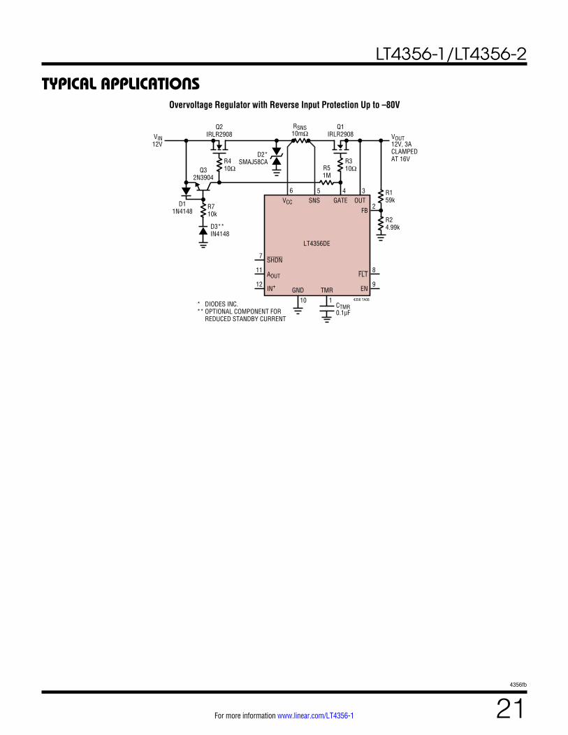
typicAl ApplicAtionsOvervoltage Regulator with Reverse Input Protection Up to –80V
CTMR0.1µF
RSNS10mΩ
Q1IRLR2908
Q2IRLR2908VIN
12VVOUT12V, 3ACLAMPEDAT 16V
4356 TA08
LT4356DE
GND TMR10 1
OUTSNSVCC
35
SHDN7
AOUT11
IN+12
6
EN
FLT
FB
9
8
2
D2*SMAJ58CA
R24.99k
R159kGATE
4
R710k
D3**IN4148
* DIODES INC.** OPTIONAL COMPONENT FOR REDUCED STANDBY CURRENT
R51M
Q32N3904
D11N4148
R310Ω
R410Ω
LT4356-1/LT4356-2
224356fb
For more information www.linear.com/LT4356-1
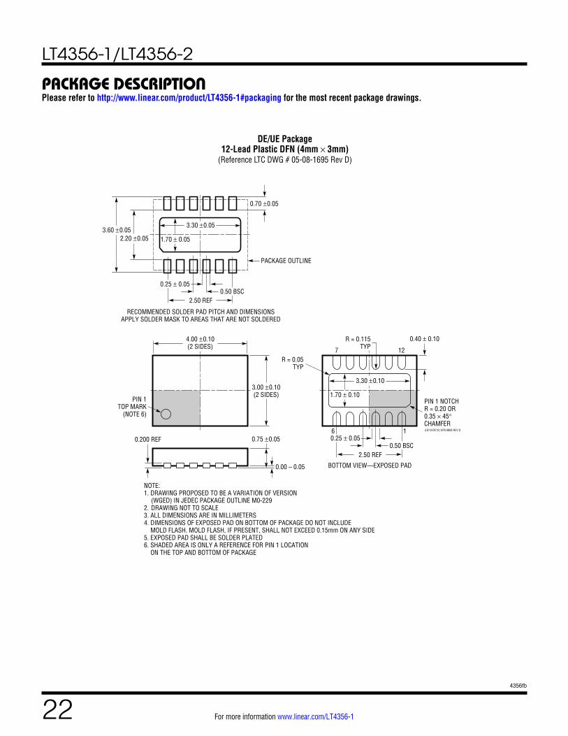
DE/UE Package12-Lead Plastic DFN (4mm × 3mm)
(Reference LTC DWG # 05-08-1695 Rev D)
4.00 ±0.10(2 SIDES)
3.00 ±0.10(2 SIDES)
NOTE:1. DRAWING PROPOSED TO BE A VARIATION OF VERSION
(WGED) IN JEDEC PACKAGE OUTLINE M0-2292. DRAWING NOT TO SCALE3. ALL DIMENSIONS ARE IN MILLIMETERS4. DIMENSIONS OF EXPOSED PAD ON BOTTOM OF PACKAGE DO NOT INCLUDE MOLD FLASH. MOLD FLASH, IF PRESENT, SHALL NOT EXCEED 0.15mm ON ANY SIDE5. EXPOSED PAD SHALL BE SOLDER PLATED6. SHADED AREA IS ONLY A REFERENCE FOR PIN 1 LOCATION ON THE TOP AND BOTTOM OF PACKAGE
0.40 ± 0.10
BOTTOM VIEW—EXPOSED PAD
1.70 ± 0.10
0.75 ±0.05
R = 0.115TYP
R = 0.05TYP
2.50 REF
16
127
PIN 1 NOTCHR = 0.20 OR0.35 × 45°CHAMFER
PIN 1TOP MARK
(NOTE 6)
0.200 REF
0.00 – 0.05
(UE12/DE12) DFN 0806 REV D
2.50 REF
RECOMMENDED SOLDER PAD PITCH AND DIMENSIONSAPPLY SOLDER MASK TO AREAS THAT ARE NOT SOLDERED
2.20 ±0.05
0.70 ±0.05
3.60 ±0.05
PACKAGE OUTLINE
3.30 ±0.10
0.25 ± 0.050.50 BSC
1.70 ± 0.05
3.30 ±0.05
0.50 BSC0.25 ± 0.05
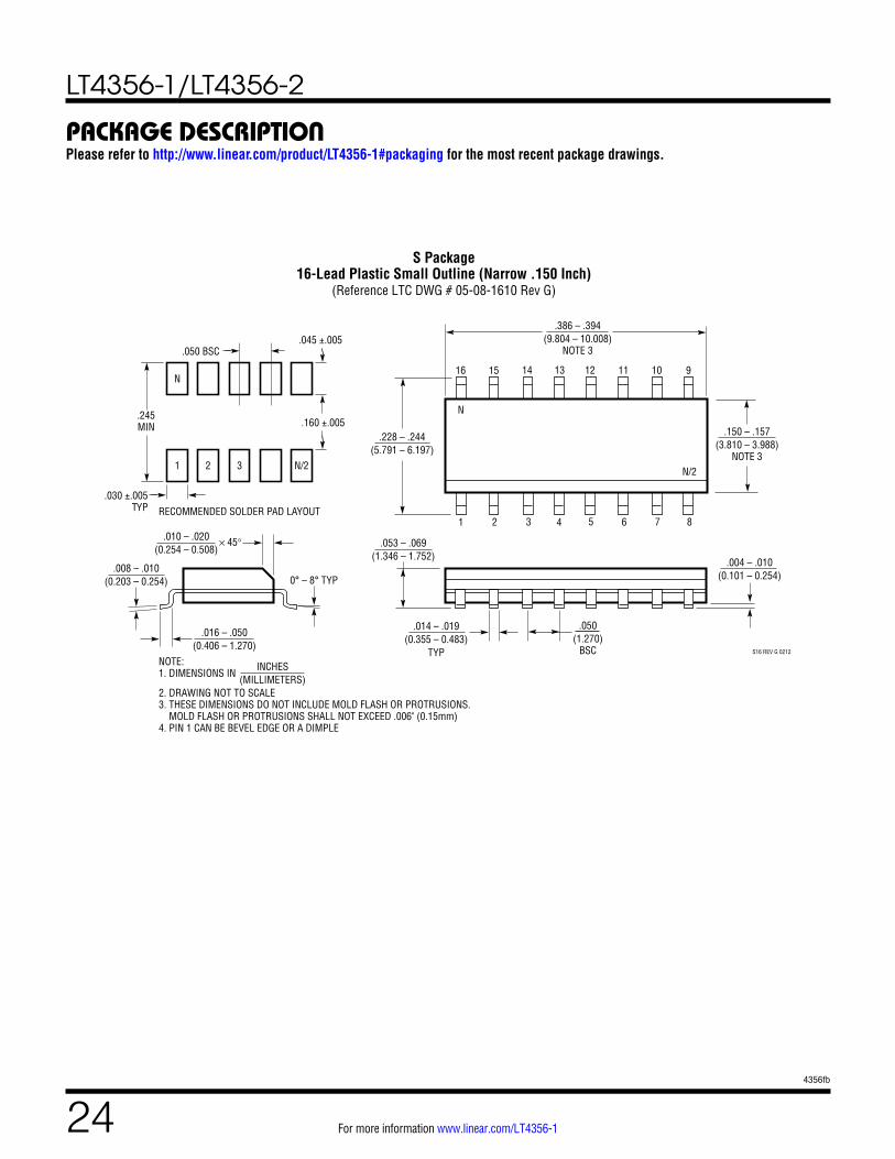
pAckAge DescriptionPlease refer to http://www.linear.com/product/LT4356-1#packaging for the most recent package drawings.
LT4356-1/LT4356-2
234356fb
For more information www.linear.com/LT4356-1
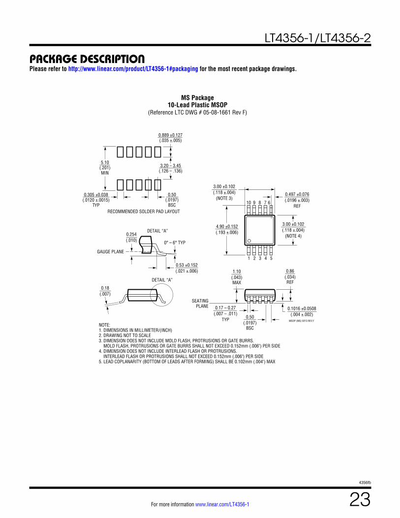
pAckAge DescriptionPlease refer to http://www.linear.com/product/LT4356-1#packaging for the most recent package drawings.
MSOP (MS) 0213 REV F
0.53 ±0.152(.021 ±.006)
SEATINGPLANE
0.18(.007)
1.10(.043)MAX
0.17 – 0.27(.007 – .011)
TYP
0.86(.034)REF
0.50(.0197)
BSC
1 2 3 4 5
4.90 ±0.152(.193 ±.006)
0.497 ±0.076(.0196 ±.003)
REF8910 7 6
3.00 ±0.102(.118 ±.004)
(NOTE 3)
3.00 ±0.102(.118 ±.004)
(NOTE 4)
NOTE:1. DIMENSIONS IN MILLIMETER/(INCH)2. DRAWING NOT TO SCALE3. DIMENSION DOES NOT INCLUDE MOLD FLASH, PROTRUSIONS OR GATE BURRS. MOLD FLASH, PROTRUSIONS OR GATE BURRS SHALL NOT EXCEED 0.152mm (.006") PER SIDE4. DIMENSION DOES NOT INCLUDE INTERLEAD FLASH OR PROTRUSIONS. INTERLEAD FLASH OR PROTRUSIONS SHALL NOT EXCEED 0.152mm (.006") PER SIDE5. LEAD COPLANARITY (BOTTOM OF LEADS AFTER FORMING) SHALL BE 0.102mm (.004") MAX
0.254(.010) 0° – 6° TYP
DETAIL “A”
DETAIL “A”
GAUGE PLANE
5.10(.201)MIN
3.20 – 3.45(.126 – .136)
0.889 ±0.127(.035 ±.005)
RECOMMENDED SOLDER PAD LAYOUT
0.305 ±0.038(.0120 ±.0015)
TYP
0.50(.0197)
BSC
0.1016 ±0.0508(.004 ±.002)
MS Package10-Lead Plastic MSOP
(Reference LTC DWG # 05-08-1661 Rev F)
LT4356-1/LT4356-2
244356fb
For more information www.linear.com/LT4356-1
pAckAge DescriptionPlease refer to http://www.linear.com/product/LT4356-1#packaging for the most recent package drawings.
.016 – .050(0.406 – 1.270)
.010 – .020(0.254 – 0.508)
× 45°
0° – 8° TYP.008 – .010
(0.203 – 0.254)
1
N
2 3 4 5 6 7 8
N/2
.150 – .157(3.810 – 3.988)
NOTE 3
16 15 14 13
.386 – .394(9.804 – 10.008)
NOTE 3
.228 – .244(5.791 – 6.197)
12 11 10 9
S16 REV G 0212
.053 – .069(1.346 – 1.752)
.014 – .019(0.355 – 0.483)
TYP
.004 – .010(0.101 – 0.254)
.050(1.270)
BSC
.245MIN
N
1 2 3 N/2
.160 ±.005
RECOMMENDED SOLDER PAD LAYOUT
.045 ±.005 .050 BSC
.030 ±.005 TYP
INCHES(MILLIMETERS)
NOTE:1. DIMENSIONS IN
2. DRAWING NOT TO SCALE3. THESE DIMENSIONS DO NOT INCLUDE MOLD FLASH OR PROTRUSIONS. MOLD FLASH OR PROTRUSIONS SHALL NOT EXCEED .006" (0.15mm)4. PIN 1 CAN BE BEVEL EDGE OR A DIMPLE
S Package16-Lead Plastic Small Outline (Narrow .150 Inch)
(Reference LTC DWG # 05-08-1610 Rev G)
LT4356-1/LT4356-2
254356fb
For more information www.linear.com/LT4356-1
Information furnished by Linear Technology Corporation is believed to be accurate and reliable. However, no responsibility is assumed for its use. Linear Technology Corporation makes no representa-tion that the interconnection of its circuits as described herein will not infringe on existing patent rights.
revision historyREV DATE DESCRIPTION PAGE NUMBER
A 05/10 Revised Features and DescriptionAdded parameters to VOL and updated Max value for VSHDN(FLT) in the Electrical Characteristics sectionRevised Pin Functions sectionReplaced Figure 6 and made text edits in the Operation and Applications Information sectionsUpdated drawings in the Typical Applications section
14, 5
810-1719, 21
B 09/17 Updated TMR pin function with minimum recommended capacitance 8
(Revision history begins at Rev A)
LT4356-1/LT4356-2
264356fb
For more information www.linear.com/LT4356-1 © LINEAR TECHNOLOGY CORPORATION 2009
LT 0917 REV B • PRINTED IN USAwww.linear.com/LT4356-1
typicAl ApplicAtion
PART NUMBER DESCRIPTION COMMENTS
LT1641-1/LT1641-2 Positive High Voltage Hot Swap Controllers Active Current Limiting, Supplies From 9V to 80V
LTC1696 Overvoltage Protection Controller ThinSOT™ Package, 2.7V to 28V
LTC1735 High Efficiency Synchronous Step-Down Switching Regulator
Output Fault Protection, 16-Pin SSOP
LTC1778 No RSENSE™ Wide Input Range Synchronous Step-Down Controller
Up to 97% Efficiency, 4V ≤ VIN ≤ 36V, 0.8V ≤ VOUT ≤ (0.9)(VIN), IOUT Up to 20A
LTC2909 Triple/Dual Inputs UV/OV Negative Monitor Pin Selectable Input Polarity Allows Negative and OV Monitoring
LTC2912/LTC2913 Single/Dual UV/OV Voltage Monitor Ads UV and OV Trip Values, ±1.5% Threshold Accuracy
LTC2914 Quad UV/OV Monitor For Positive and Negative Supplies
LTC3727/LTC3727-1 2-Phase, Dual, Synchronous Controller 4V ≤ VIN ≤ 36V, 0.8V ≤ VOUT ≤ 14V
LTC3827/LTC3827-1 Low IQ, Dual, Synchronous Controller 4V ≤ VIN ≤ 36V, 0.8V ≤ VOUT ≤ 10V, 80µA Quiescent Current
LTC3835/LTC3835-1 Low IQ, Synchronous Step-Down Controller Single Channel LTC3827/LTC3827-1
LT3845 Low IQ, Synchronous Step-Down Controller 4V ≤ VIN ≤ 60V, 1.23V ≤ VOUT ≤ 36V, 120µA Quiescent Current
LTC3850 Dual, 550kHz, 2-Phase Synchronous Step-Down Controller
Dual 180° Phased Controllers, VIN 4V to 24V, 97% Duty Cycle, 4mm × 4mm QFN-28, SSOP-28 Packages
LT4256-1/LT4256-2 Positive 48V Hot Swap Controller with Open-Circuit Detect
Foldback Current Limiting, Open-Circuit and Overcurrent Fault Output, Up to 80V Supply
LTC4260 Positive High Voltage Hot Swap Controller with ADC and I2C
Wide Operating Range 8.5V to 80V
LTC4352 Ideal MOSFET ORing Diode External N-channel MOSFETs Replace ORing Diodes, 0V to 18V Operation
LTC4354 Negative Voltage Diode-OR Controller Controls Two N-channel MOSFETs, 1µs Turn-Off, 80V Operation
LTC4355 Positive Voltage Diode-OR Controller Controls Two N-channel MOSFETs, 0.5µs Turn-Off, 80V Operation
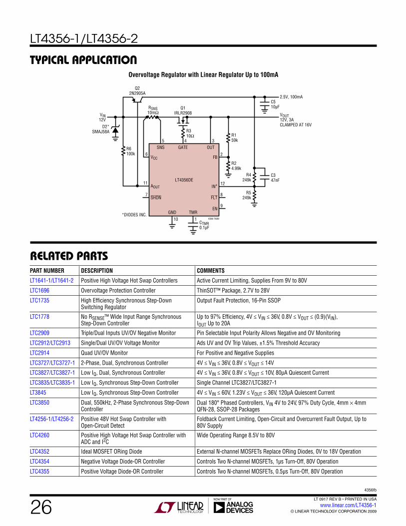
Overvoltage Regulator with Linear Regulator Up to 100mA
CTMR0.1µF
R310Ω
RSNS10mΩ
Q22N2905A
VIN12V
VOUT12V, 3ACLAMPED AT 16V
2.5V, 100mA
4356 TA09
LT4356DE
GND TMR10 1
OUTGATESNS345
AOUT11
SHDN7
VCC6
EN
FLT
FB
9
IN+ 12
8
2
C510µF
R24.99k
R6100k
R159k
R5249k
R4249k
C347nF
Q1IRLR2908
D2*SMAJ58A
*DIODES INC.
relAteD pArts


![Untitled-2 [suntracbatteries.com]suntracbatteries.com/suntrac.pdf · capacity 12v 20ah 12v 40ah 12v 60ah 12v b40ah 12v b60ah 12v b80ah 12v biooah 12v 80ah 12v iooah 12v 130ah 12v](https://img.pdfslide.us/doc/110x75/603efb7aa12c32391f5484d1/untitled-2-capacity-12v-20ah-12v-40ah-12v-60ah-12v-b40ah-12v-b60ah-12v-b80ah.jpg)