Embed Size (px)
Citation preview

LT3509
13509fc
TYPICAL APPLICATION
FEATURES
APPLICATIONS
DESCRIPTION
Dual 36V, 700mAStep-Down Regulator
The LT®3509 is a dual, current mode, step-down switching regulator, with internal power switches each capable of providing 700mA output current. This regulator provides a compact and robust solution for multi-rail systems in harsh environments. It incorporates several protection features including overvoltage lockout and cycle-by-cycle current limit. Thermal shutdown provides additional protection. The loop compensation components and the boost diodes are integrated on-chip. Switching frequency is set by a single external resistor. External synchronization is also possible. The high maximum switching frequency allows the use of small inductors and ceramic capacitors for low ripple. Constant frequency operation above the AM band avoids interference with radio reception, making the LT3509 well suited for automotive applications. Each regulator has an independent shutdown and soft-start control pin. When both converters are powered down, the common circuitry enters a low current shutdown state.
3.3V and 5V Dual Output Step-Down Converter
n Two 700mA Switching Regulators with Internal Power Switches
n Wide 3.6V to 36V Operating Rangen Overvoltage Lockout Protects Circuit Through 60V
Supply Transientsn Short-Circuit Robustn Low Dropout Voltage: 95% Maximum Duty Cyclen Adjustable 300kHz to 2.2MHz Switching Frequency
Synchronizable Over the Full Rangen Uses Small Inductors and Ceramic Capacitorsn Integrated Boost Diodes n Internal Compensationn Thermally Enhanced 14-Lead (4mm × 3mm)
DFN and 16 Lead MSOP Packages
n Automotive Electronicsn Industrial Controlsn Wall Transformer Regulationn Networking Devicesn CPU, DSP, or FPGA Power
3509 TA01a
LT3509
GND
DA1
FB1
RUN/SS1
SYNC
DA2
FB2
RUN/SS2
RT
BDVIN
BOOST2BOOST1
SW2SW1
10μH
fSW = 700kHz
0.1μF0.1μF
6.5V TO 36V(TRANSIENT TO 60V)
2.2μF
6.8μH3.3V
700mA5V700mA
10μF
10.2k
31.6k 53.6k
MBRM140MBRM140
1nF
22μF
10.2k60.4k
1nF
LOAD CURRENT (A)
0.0
EFF
ICIE
NC
Y (
%)
70
75
80
0.7
3509 TA01b
60
65
50
55
0.1 0.2 0.6
90
85
0.50.40.3
VOUT = 3.3V
VOUT = 5V
VIN = 12VfSW = 700kHz
Effi ciency
L, LT, LTC, LTM, Burst Mode, Linear Technology and the Linear logo are registered trademarks of Linear Technology Corporation. All other trademarks are the property of their respective owners.
www.BDTIC.com/Linear

LT3509
23509fc
ABSOLUTE MAXIMUM RATINGS
VIN Pin (Note 2) ........................................................60VBD Pin .......................................................................20VBOOST Pins ..............................................................60VBOOST Pins above SW .............................................30VRUN/SS, FB, RT, SYNC pins ........................................6VOperating Junction Temperature Range (Notes 3, 6)
LT3509E ............................................ –40°C to 125°CLT3509I ............................................. –40°C to 125°CLT3509H ............................................ –40°C to 150°C
PIN CONFIGURATION
ORDER INFORMATIONLEAD FREE FINISH TAPE AND REEL PART MARKING* PACKAGE DESCRIPTION TEMPERATURE RANGE
LT3509EDE#PBF LT3509EDE#TRPBF 3509 14-Lead (4mm × 3mm) Plastic DFN –40°C to 125°C
LT3509IDE#PBF LT3509IDE#TRPBF 3509 14-Lead (4mm × 3mm) Plastic DFN –40°C to 125°C
LT3509EMSE#PBF LT3509EMSE#TRPBF 3509 16-Lead Plastic MSOP with Exposed Pad –40°C to 125°C
LT3509IMSE#PBF LT3509IMSE#TRPBF 3509 16-Lead Plastic MSOP with Exposed Pad –40°C to 125°C
LT3509HMSE#PBF LT3509HMSE#TRPBF 3509 16-Lead Plastic MSOP with Exposed Pad –40°C to 150°C
Consult LTC Marketing for parts specifi ed with wider operating temperature ranges. *The temperature grade is identifi ed by a label on the shipping container.
Consult LTC Marketing for information on non-standard lead based fi nish parts.
For more information on lead free part marking, go to: http://www.linear.com/leadfree/ For more information on tape and reel specifi cations, go to: http://www.linear.com/tapeandreel/
Storage Temperature Range .................. –65°C to 150°CLead Temperature (Soldering, 10 sec.)
MSOP Package ................................................. 300°C
1
2
3
4
5
6
7
14
13
12
11
10
9
8
FB1
RUN/SS1
BD
SYNC
RT
RUN/SS2
FB2
DA1
BOOST1
SW1
VIN
SW2
BOOST2
DA2
TOP VIEW
DE14 PACKAGE14-LEAD (4mm × 3mm) PLASTIC DFN
15
θJA = 43°C/W, θJC = 4.3°C/WEXPOSED PAD (PIN 15) IS GND, MUST BE SOLDERED TO PCB
12345678
DA1BOOST1
SW1VINVIN
SW2BOOST2
DA2
161514131211109
FB1RUN/SS1AGNDBDSYNCRTRUN/SS2FB2
TOP VIEW
MSE PACKAGE16-LEAD PLASTIC MSOP
17
θJA = 43°C/W, θJC = 4.3°C/WEXPOSED PAD (PIN 17) IS GND, MUST BE SOLDERED TO PCB
(Note 1)
www.BDTIC.com/Linear

LT3509
33509fc
ELECTRICAL CHARACTERISTICS
Note 1: Stresses beyond those listed under Absolute Maximum Ratings
may cause permanent damage to the device. Exposure to any Absolute
Maximum Rating condition for extended periods may affect device reliability
and lifetime.
Note 2. Absolute Maximum Voltage at the VIN pin is 60V for non-repetitive
1 second transients and 36V for continuous operation.
Note 3. The LT3509E is guaranteed to meet performance specifi cations from
0°C to 125°C junction temperature. Specifi cations over the –40°C to 125°C
operating junction temperature range are assured by design, characterization
and correlation with statistical process controls. The LT3509I is guaranteed
over the full –40°C to 125°C temperature range. The LT3509H is guaranteed
The l denotes the specifi cations which apply over the full operating temperature range, otherwise specifi cations are at TA = 25°C, VIN = 12V. (Note 3)
PARAMETER CONDITIONS MIN TYP MAX UNITS
VIN Undervoltage Lockout 3.3 3.6 V
VIN Overvoltage Lockout 37 38.5 40 V
Input Quiescent Current Not Switching VFB > 0.8V 1.9 2.2 mA
Input Shutdown Current V(RUN/SS[1,2]) < 0.3V 9 15 μA
Feedback Pin Voltage l 0.784 0.8 0.816 V
Reference Voltage Line Regulation 3.6V < VIN < 36V 0.01 %/V
RUN/SS Shutdown Threshold 0.4 0.6 0.8 V
RUN/SS Voltage for Full IOUT 2 V
RUN/SS Pin Pull-up Current 0.7 1 1.3 μA
Feedback Pin Bias Current (Note 4) VFB = 0.8V l 90 500 nA
Switch Current Limit l 1.05 1.4 1.9 A
DA Comparator Current Threshold 0.7 0.95 1.2 A
Boost Pin Current ISW = 0.9A 22 36 mA
Switch Leakage Current 0.01 1.0 μA
Switch Saturation Voltage ISW = 0.9A (Note 5) 0.32 V
Minumum Boost Voltage above Switch ISW = 0.9A 1.5 2.2 V
Boost Diode Forward Voltage IBD= 20mA 0.7 0.9 V
Boost Diode Leakage VR = 30V 0.1 5 μA
Switching Frequency RT = 40.2kΩRT = 180kΩRT = 14.1kΩ
l 0.922372.0
1.02602.15
1.082902.5
MHzkHz
MHz
Sync Pin Input Threshold 1.0 V
Switch Minimum Off-Time l 80 150 ns
over the full –40°C to 150°C operating junction temperature range. High
junction temperatures degrade operating lifetimes. Operating lifetime is
derated at junction temperatures greater than 125°C.
Note 4. Current fl ows out of pin.
Note 5. Switch Saturation Voltage is guaranteed by design.
Note 6. This IC includes overtemperature protection that is intended to protect
the device during momentary overload conditions. Junction temperature will
exceed the maximum operating temperature when overtemperature protection
is active. Continuous operation above the specifi ed maximum operating
junction temperature may impair device reliability.
www.BDTIC.com/Linear

LT3509
43509fc
TYPICAL PERFORMANCE CHARACTERISTICS
ILOAD(A)0
EFFI
CIEN
CY (%
)
0.8
3509 G01
65
70
75
80
85
90
600.2 0.4 0.6
95
VIN = 12V
TA = 25ºC
VIN = 24V
ILOAD(A)0
EFFI
CIEN
CY (%
)
0.8
3509 G02
60
65
70
75
80
85
90
550.2 0.4 0.6
95
VIN = 12V
TA = 25ºC
ILOAD(A)0
EFFI
CIEN
CY (%
)
0.8
3509 G03
55
60
65
70
75
80
85
500.2 0.4 0.6
90
VIN = 12V
TA = 25ºC
ISW(A)0
VC
E(S
AT) (
V)
1.00.8
3509 G04
0.05
0.1
0.15
0.2
0.25
0.3
00.2 0.4 0.6
0.35TA = 25ºC
ISW(A)0
I BO
OS
T (m
A)
0.8 1
3509 G05
5
10
15
20
00.2 0.4 0.6
25TA = 25ºC
BOOST DIODE CURRENT (mA)0
Vf (
V)
100 150
3509 G06
0.2
0.4
0.6
0.8
1
050
1.2TA = 25ºC
RT(kΩ)
0
FREQ
UEN
CY
(M
Hz)
120 140100 160 180
3509 G07
0.5
1.0
1.5
2.0
2.2
060 8020 40
TA = 25ºC
Effi ciency vs Load CurrentVOUT = 5V, fSW = 2.0MHz
Effi ciency vs Load CurrentVOUT = 3.3V, fSW = 2.0MHz
Effi ciency vs Load CurrentVOUT = 1.8V, fSW = 0.7MHz
Switch VCE(SAT) vs ISW IBOOST vs ISW
Boost Diode Characteristics Frequency vs RT
www.BDTIC.com/Linear

LT3509
53509fc
FB Pin Voltage vs TemperaturefSW vs Temperature (Measured at 1MHz)
TYPICAL PERFORMANCE CHARACTERISTICS
ILOAD (A)0
MA
XIM
UM
VIN
(V)
0.60.4 0.8
3509 G10
5
10
15
20
25
00.2
30TA = 25ºC
TA = 85ºC
ILOAD (A)0
MA
XIM
UM
VIN
(V)
3509 G11
5
10
15
20
25
0
45
30
35
40TA = 25ºC
TA = 85ºC
0.60.4 0.80.2
Max VIN for Constant FrequencyVOUT = 3.3V, fSW = 2MHz
Max VIN for Constant FrequencyVOUT = 5V, fSW = 2MHz
Minimum On-Time vs Temperature, ILOAD = 0.3A
DUTY CYCLE (%)0 10
I LIM
(A)
100
3509 G14
0.2
0.4
0.6
0.8
1
1.2
1.4
1.6
020 30 40 50 60 70 80 90
1.8TA = 25ºC
ILIM vs Temperature ILIM vs Duty Cycle
TEMPERATURE (°C)
–500.790
FEED
BA
CK
PIN
VO
LTA
GE (
V)
0.795
0.800
0.805
0.810
–25 0 25 50
3509 G08
75 100 125 150
TEMPERATURE (˚C)
–50
NO
RM
ALIZ
ED
(f S
W)
1.01
1.02
1.03
25 50 75 100 125
3509 G09
1.00
0.99
–25 0 150
0.98
0.97
1.04
TEMPERATURE (°C)
–50
MIN
IMU
M O
N-T
IME (
ns)
80
120
150
3509 G12
40
00 50 100–25 25 75 125
160
60
100
20
140
TEMPERATURE (°C)–50
I LIM
(A) 1.0
1.3
1.5
25 75 150
3509 G13
0.9
0.7
0.5–25 0 50 100 125
SWITCH
DA
www.BDTIC.com/Linear

LT3509
63509fc
PIN FUNCTIONSDA1, DA2 (Pins 1, 7/Pins 1, 8): The DA pins are the anode connections for the catch diodes. These are connected internally to the exposed ground pad by current sensing resistors.
BOOST1, BOOST2 (Pins 2, 6/Pins 2, 7): The BOOST pins are used to dynamically boost the power transistor base above VIN to minimize the voltage drop and power loss in the switch. These should be tied to the associated switch pins through the boost capacitors.
SW1, SW2 (Pins 3, 5/Pins 3, 6): The SW pins are the internal power switch outputs. These should be connected to the associated inductors, catch diode cathodes, and the boost capacitors.
VIN (Pin 4/Pins 4, 5): The VIN pins supply power to the internal power switches and control circuitry. In the MSE package the VIN pins must be tied together. The input capacitor should be placed as close as possible to the supply pins.
FB1, FB2 (Pins 14, 8/Pins 16, 9): The FB pins are used to set the regulated output voltage relative to the internal reference. These pins should be connected to a resistor divider from the regulated output such that the FB pin is at 0.8V when the output is at the desired voltage.
RUN/SS1, RUN/SS2 (Pins 13, 9/Pins 15, 10): The RUN/SS pins enable the associated regulator channel. If both pins are pulled to ground, the device will shut-down to a low power state. In the range 0.8V to 2V, the regulators are enabled but the peak switch current and the DA pin maxi-mum current are limited to provide a soft-start function. Above 2V, the full output current is available. The inputs incorporate a 1μA pull-up so that they will fl oat high or charge an external capacitor to provide a current limited
soft-start. The pins are pulled down by approximately 250μA in the case of overvoltage or overtemperature conditions in order to discharge the soft-start capacitors. The pins can also be driven by a logic control signal of up to 5.0V. In this case, it is necessary place a 10k to 50k resistor in series along with a capacitor from the RUN/SS pin to ground to ensure that there will be a soft-start for both initial turn on and in the case of fault conditions. Do not tie these pins to VIN.
RT (Pin 10/Pin 11): The RT pin is used to set the internaloscillator frequency. A 40.2k resistor from RT to ground results in a nominal frequency of 1MHz.
SYNC (Pin 11/Pin12): The SYNC pin allows the switching frequency to be synchronized to a external clock. Choose RT resistor to set a free-run frequency at least 12% less than the external clock frequency for correct operation.
BD (Pin 12/Pin 13): The BD pin is common anode connec-tion of the internal Schottky boost diodes. This provides the power for charging the BOOST capacitors. It should be locally bypassed for best performance.
Exposed Pad (Pin 15/Pin 17): GND. This is the reference and supply ground for the regulator. The exposed pad must be soldered to the PCB and electrically connected to supply ground. Use a large ground plane and thermal vias to optimize thermal performance. The current in the catch diodes also fl ows through the GND pad to the DA pins.
AGND (Pin 14, MSOP Package Only): This is the connected to the ground connection of the chip and may be used as a separate return for the low current control side components. It should not be used as the only ground connection or as a connection return for load side components.
(DFN/MSOP)
www.BDTIC.com/Linear

LT3509
73509fc
BLOCK DIAGRAM
SHUTDOWNAND
SOFT-STARTCONTROL
OVERVOLTAGEDETECT
COMMONCIRCUITRY
1 OF 2 REGULATOR CHANNELS SHOWN
SWITCHLOGIC
CLAMP
–17mV
18mΩ
GND
BD
VREF0.8V
SWITCHDRIVER
ERRORAMPLIFIER
DA CURRENTCOMPARATOR
L1
D1
R1
R2
MAIN CURRENTCOMPARATOR
POWERSWITCH
BOOSTDIODE
BOOST
SW
DA C5
FB
VC
SLOPE
RT
RT
SYNC
C3
C4
C1
RUN/SS2
RUN/SS1
VIN
VOUT
VREF ANDCORE
VOLTAGEREGULATOR
OSCILLATOR
–
3509 BD
C2
NOTE: THE BD PIN
IS COMMON TO
BOTH CHANNELS
Figure 1. Functional Block Diagram
www.BDTIC.com/Linear

LT3509
83509fc
OPERATIONOverview
The LT3509 is a dual, constant frequency, current mode switching regulator with internal power switches. The two independent channels share a common voltage reference and oscillator and operate in phase. The switching frequency is set by a single resistor and can also be synchronized to an external clock. Operation can be best understood by referring to the Block Diagram (Figure 1).
Startup and Shutdown
When the RUN/SS[1,2] pins are pulled low (<0.4V) the associated regulator channel is shut down. If both channels are shut down, the common circuitry also enters a low current state. When the RUN/SS pins exceed approximately 0.8V, the common circuitry and the associated regulator are enabled but the output current is limited. From 0.8V up to 2.0V the current limit increases until it reaches the full value. The RUN/SS pins also incorporate a 1μA pull-up to approximately 3V, so the regulator will run if they are left open. A capacitor to ground will cause a current limited soft-start to occur at power-up. In the case of undervoltage, overvoltage or overtemperature conditions the internal circuitry will pull the RUN/SS pins down with a current of approximately 250μA. Thus a new soft-start cycle will occur when the fault condition ends.
Voltage and Current Regulation
The power switches are controlled by a current-mode regulator architecture. The power switch is turned on at the beginning of each clock cycle and turned off by the main current comparator. The inductor current will ramp up while the switch is on until it reaches the peak current threshold. The current at which it turns off is determined by the error amp and the internal compensation network. When the switch turns off, the current in the inductor will cause the SW pin to fall rapidly until the catch diode, D1, conducts. The voltage applied to the inductor will now reverse and the current will linearly fall. The resistor divider, R1 and R2, sets the desired output voltage such
that when the voltage at FB reaches 0.8V, the main current comparator threshold will fall and reduce the peak inductor current and hence the average current, until it matches the load current. By making current the controlled variable in the loop, the inductor impedance is effectively removed from the transfer function and the compensation network is simplifi ed. The main current comparator threshold is reduced by the slope compensation signal to eliminate sub-harmonic oscillations at duty cycles >50%.
Current Limiting
Current mode control provides cycle-by-cycle current limiting by means of a clamp on the maximum current that can be provided by the switch. A comparator monitors the current fl owing through the catch diode via the DA pin. This comparator delays switching if the diode current is higher than 0.95A (typical). This current level is indicative of a fault condition such as a shorted output with a high input voltage. Switching will only resume once the diode current has fallen below the 0.95A limit. This way the DA comparator regulates the valley current of the inductor to 0.95A during a short circuit. This will ensure the part will survive a short-circuit event.
Over and Undervoltage Shutdown
A basic undervoltage lockout prevents switching if VIN is below 3.3V (typical). The overvoltage shutdown stops the part from switching when VIN is greater than 38.5V (typical). This protects the device and its load during momentary overvoltage events. After the input voltage falls below 38.5V, the part initiates a soft start sequence and resumes switching.
BOOST Circuit
To ensure best effi ciency and minimum dropout voltage the output transistor base drive is boosted above VIN by the external boost capacitors (C4). When the SW pin is low the capacitors are charged via the BOOST diodes and the supply on BD.
www.BDTIC.com/Linear
LT3509
93509fc
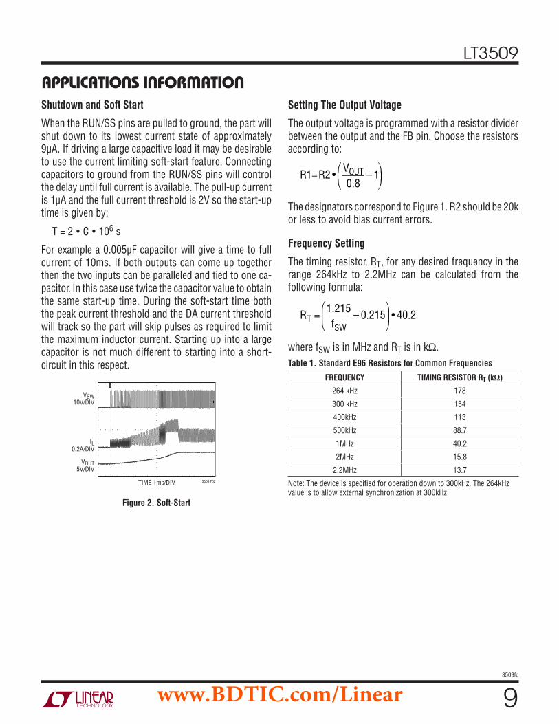
APPLICATIONS INFORMATIONShutdown and Soft Start
When the RUN/SS pins are pulled to ground, the part will shut down to its lowest current state of approximately 9μA. If driving a large capacitive load it may be desirable to use the current limiting soft-start feature. Connecting capacitors to ground from the RUN/SS pins will control the delay until full current is available. The pull-up current is 1μA and the full current threshold is 2V so the start-up time is given by:
T = 2 • C • 106 s
For example a 0.005μF capacitor will give a time to full current of 10ms. If both outputs can come up together then the two inputs can be paralleled and tied to one ca-pacitor. In this case use twice the capacitor value to obtain the same start-up time. During the soft-start time both the peak current threshold and the DA current threshold will track so the part will skip pulses as required to limit the maximum inductor current. Starting up into a large capacitor is not much different to starting into a short-circuit in this respect.
Setting The Output Voltage
The output voltage is programmed with a resistor divider between the output and the FB pin. Choose the resistors according to:
R1=R2 •VOUT0.8
– 1
The designators correspond to Figure 1. R2 should be 20k or less to avoid bias current errors.
Frequency Setting
The timing resistor, RT , for any desired frequency in the range 264kHz to 2.2MHz can be calculated from thefollowing formula:
RT =1.215fSW
– 0.215 • 40.2
where fSW is in MHz and RT is in kΩ.
Table 1. Standard E96 Resistors for Common Frequencies
FREQUENCY TIMING RESISTOR RT (kΩ)
264 kHz 178
300 kHz 154
400kHz 113
500kHz 88.7
1MHz 40.2
2MHz 15.8
2.2MHz 13.7
Note: The device is specifi ed for operation down to 300kHz. The 264kHz value is to allow external synchronization at 300kHz
Figure 2. Soft-Start
IL0.2A/DIV
VSW10V/DIV
VOUT5V/DIV
TIME 1ms/DIV 3509 F02
www.BDTIC.com/Linear

LT3509
103509fc
APPLICATIONS INFORMATIONExternal Synchronization
The external synchronization provides a trigger to the internal oscillator. As such, it can only raise the frequency above the free-run value. To allow for device and component tolerances, the free run frequency should be set to at least 12% lower than the lowest supplied external synchronization reference. The oscillator and hence the switching frequency can then pushed up from 12% above the free-run frequency, set by the selected RT. For example, if the minimum external clock is 300kHz, the RT should be chosen for 264kHz.
The SYNC input has a threshold of 1.0V nominal so it is compatible with most logic levels. The duty cycle is not critical provided the high or low pulse width is at least 80ns.
Design Procedure
Before starting detailed design a number of key design parameters should be established as these may affect design decisions and component choices along the way. One of the main things to determine apart from the desired output voltages is the input voltage range. Both the normal operating range and the extreme conditions of surges and/or dips or brown-outs need to be known. Then the operating frequency should be considered and if there are particular requirements to avoid interference. If there are very specifi c frequencies that need to be avoided then external synchronization may be needed. This could also be desirable if multiple switchers are used as low frequency beating between similar devices can be undesirable. For effi cient operation this converter requires a boost supply so that the base of the output transistor can be pumped above the input voltage during the switch on time. Depending
on the input and output voltages the boost supply can be provided by the input voltage, one of the regulated outputs or an independent supply such as an LDO.
Input Voltage Range
Firstly, the LT3509 imposes some hard limits due to the undervoltage lock-out and the overvoltage protection. A given application will also have a reduced, normal operating range over which maximum effi ciency and lowest ripple are obtained. This usually requires that the device is operating at a fi xed frequency without skipping pulses. There may also be zones above and below the normal range where regulation is maintained but effi ciency and ripple may be compromised. At the low end, insuffi cient input voltage will cause loss of regulation and increased ripple—this is the dropout range. At the high end if the duty cycle becomes too low this will cause pulse skipping and excessive ripple. This is the pulse-skip region. Both situations also lead to higher noise at frequencies other than the chosen switching frequency. Occasional excursions into pulse-skip mode, during surges for example, may be tolerable. Pulse skipping will also occur at light loads even within the normal operating range but ripple is usually not degraded because at light load the output capacitor can hold the voltage steady between pulses.
For input voltages greater than 30V, there are restrictions on the inductor value. See the Inductor Selection section for details.
To ensure the regulator is operating in continuous mode it is necessary to calculate the duty cycle for the required output voltage over the full input voltage range. This must then be compared with minimum and maximum practical duty cycles.
www.BDTIC.com/Linear

LT3509
113509fc
APPLICATIONS INFORMATIONIn any step-down switcher the duty cycle when operating in continuous, or fi xed frequency, mode is dependent on the step-down ratio. This is because for a constant average load current the decay of the inductor current when the switch is off must match the increase in inductor current when the switch is on. The can be estimated by the following formula:
DCV V
V V VOUT F
IN SW F=
+
− +
where:
DC = Duty Cycle (Fraction of Cycle when Switch is On)
VOUT = Output Voltage
VIN = Input Voltage
VF = Catch Diode Forward Voltage
VSW = Switch Voltage Drop
Note: This formula neglects switching and inductor losses so in practice the duty cycle may be slightly higher.
It is clear from this equation that the duty cycle will approach 100% as the input voltage is reduced and become smaller as the input voltage increases. There are practical limits to the minimum and maximum duty cycles for continuous operation due to the switch minimum off and on times. These are independent of operating frequency so it is clear that range of usable duty cycle is inverserly proportional to frequency. Therefore at higher frequency the input voltage range (for constant frequency operation) will narrow.
The minimum duty cycle is given by:
DC f tMIN SW ON MIN= • ( )
where:
fSW = Switching Frequency
tON(MIN) = Switch Minimum On-Time
The minimum on time increases with increasing tempera-ture so the value for the maximum operating temperature should be used. See the Minimum On-Time vs Temperature graph in the Typical Performance Characteristics.
The maximum input voltage for this duty cycle is given by:
VV V
DCV VIN MAX
OUT F
MINF SW( ) =
+− +
Above this voltage the only way the LT3509 can maintain regulation is to skip cycles so the effective frequency will reduce. This will cause an increase in ripple and the switch-ing noise will shift to a lower frequency. This calculation will in practice drive the maximum switching frequency for a desired step-down ratio.
Figure 3. Continuous Mode
IL0.5A/DIV
VOUT100mV/DIV
(AC COUPLED)
TIME 1μs/DIV 3509 F03
Figure 4. Pulse Skipping
IL0.5A/DIV
VOUT100mV/DIV
(AC COUPLED)
TIME 1μs/DIV 3509 F04
www.BDTIC.com/Linear

LT3509
123509fc
APPLICATIONS INFORMATIONMinimum Input Voltage and Boost Architecture
The minimum operating voltage is determined either by the LT3509’s internal undervoltage lockout of ~3.6V or by its maximum duty cycle. The maximum duty cycle for fi xed frequency operation is given by:
DC t fMAX OFF MIN SW= −1 ( ) •
It follows that:
VV VDC
V VIN MINOUT F
MAXF SW( ) =
+− +
If a reduction in switching frequency can be tolerated the minimum input voltage can drop to just above output voltage. Not only is the output transistor base pumped above the input voltage by the boost capacitor, the switch can remain on through multiple switching cycles resulting in a high effective duty cycle. Thus, this is a true low dropout regulator. As it is necessary to recharge the boost capacitor from time to time, a minimum width off-cycle will be forced occasionally to maintain the charge. Depending on the operating frequency, the duty cycle can reach 97% to 98%, although at this point the output pulses will be at a sub-multiple of the programmed frequency. One other consideration is that at very light loads or no load the part will go into pulse skipping mode. The part will then have trouble getting enough voltage on to the
boost capacitors to fully saturate the switch. This is most problematic when the BD pin is supplied from the regulated output. The net result is that a higher input voltage will be required to start up the boost system. The typical minimum input voltage over a range of loads is shown in Figure 5 for 3.3V and Figure 6 for 5V.
When operating at such high duty cycles the peak currents in the boost diodes are greater and this will require a the BD supply to be somewhat higher than would be required at less extreme duty cycles. If operation at low input/output ratios and low BD supply voltages is required it may be desirable to augment the internal boost diodes with external discrete diodes in parallel.
Boost Pin Considerations
The boost capacitor, in conjunction with the internal boost diode, provides a bootstrapped supply for the power switch that is above the input voltage. For operation at 1MHz and above and at reasonable duty cycles a 0.1μF capacitor will work well. For operation at lower frequencies and/or higher duty cycles something larger may be needed. A good rule of thumb is:
CfBOOSTSW
=1
10 •
where fSW is in MHz and CBOOST is in μF
Figure 5. Minimum VIN for 3.3V VOUT
LOAD CURRENT (A)
0.001
VIN
TO
STA
RT (
V)
4
4.5
5
1
3509 F05
3
3.5
2.5
20.01 0.1
5.5
TO START
TO RUN
Figure 6. Minimum VIN for 5V VOUT
LOAD CURRENT (A)
0.001
VIN
TO
STA
RT (
V)
6
6.5
1
3509 F06
5
5.5
4.5
40.01 0.1
7
TO START
TO RUN
www.BDTIC.com/Linear

LT3509
133509fc
APPLICATIONS INFORMATION
Figure 7. BD Tied to Regulated Output
L1
D1COUT
VOUT
CBOOST
VBOOST – VSW VOUT
MAX VBOOST VIN VOUT
VOUT 3V
VIN
3509 F07
LT3509
GND
VIN
BD
BOOST
SW
DA
CIN
Boost Pin Considerations
Figure 7 through Figure 9 show several ways to arrange the boost circuit. The BOOST pin must be more than 2V above the SW pin for full effi ciency. For outputs of 3.3V and higher, the standard circuit Figure 7 is best. For lower output voltages, the boost diode can be tied to the input Figure 8. The circuit in Figure 7 is more effi cient because the boost pin current comes from a lower voltage source. Finally, as shown in Figure 9, the BD pin can be tied to another source that is at least 3V. For example, if you are generating 3.3V and 1.8V, and the 3.3V is on whenever the 1.8V is on, the 1.8V boost diode can be connected to the 3.3V output.
In any case, be sure that the maximum voltage at the BOOST pin is less than 60V and the voltage difference between the BOOST and SW pins is less than 30V.
Inductor Selection and Maximum Output Current
A good fi rst choice for the inductor value is:
L V VMHz
fOUT FSW
= +( ) •.2 1
where VF is the voltage drop of the catch diode (~0.5V) and L is in μH.
The inductor’s RMS current rating must be greater than the maximum load current and its saturation current should be at least 30% higher. For highest effi ciency, the series resistance (DCR) should be less than 0.15Ω. Table 2 lists
several vendors and types that are suitable.
The current in the inductor is a triangle wave with an average value equal to the load current. The peak switch current is equal to the output current plus half the peak-to-peak inductor ripple current. The LT3509 limits its switch current in order to protect itself and the system from overcurrent faults. Therefore, the maximum output current that the LT3509 will deliver depends on the switch current limit, the inductor value and the input and output voltages.
L1
D1COUT
VOUT
CBOOST
VBOOST – VSW VIN
MAX VBOOST 2VIN
CIN
VIN
3509 F08
LT3509
GND
VIN
BD
BOOST
SW
DA
Figure 8. Supplied from VIN
L1
D1
COUT
VOUT
CBOOST
VBOOST – VSW VBD
MAX VBOOST VIN VBD
VBD 3V
CIN
VIN
VBD
3509 F09
LT3509
GND
VIN
BD
BOOST
SW
DA
Figure 9. Separate Boost Supply
www.BDTIC.com/Linear

LT3509
143509fc
When the switch is off, the potential across the inductor is the output voltage plus the catch diode forward voltage. This gives the peak-to-peak ripple current in the inductor:
ΔIL =(1– DC)
VOUT + VFL • fSW
where:
DC = Duty Cycle
fSW = Switching Frequency
L = Inductor Value
VF = Diode Forward Voltage
The peak inductor and switch current is:
ISWPK =ILPK =IOUT +
ΔIL2
To maintain output regulation, this peak current must be less than the LT3509’s switch current limit ILIM. This is dependent on duty cycle due to the slope compensation. For ILIM is at least 1.4A at low duty cycles and decreases linearly to 1.0A at DC = 0.8.
The theoretical minimum inductance can now be calcu-lated as:
LDC
fV VI IMIN
MIN OUT F
LIM OUT=
+1–•
–
where DCMIN is the minimum duty cycle called for by the application i.e.:
DCV V
V V VMINOUT MAX F
IN MIN SW F=
+
+( )
( ) –
There is a limit to the actual minimum duty cycle imposed by the minimum on-time of the switch. For a robust design it is important that inductor that will not saturate when the switch is at its minimum on-time, the input voltage is at maximum and the output is short circuited. In this case the full input voltage, less the drop in the switch, will appear across the inductor. This doesn’t require an actual short, just starting into a capacitive load will provide the same conditions. The Diode current sensing scheme will ensure that the switch will not turn-on if the inductor current is above the DA current limit threshold, which has a maximum of 1.1A. The peak current under short-circuit conditions can then be calculated from:
I
V t
LAPEAK
IN ON MIN= +•
.( ) 1 1
The inductor should have a saturation current greater than this value. For safe operation with high input voltages this can often mean using a physically larger inductor as higher value inductors often have lower saturation currents for a given core size. As a general rule the saturation current should be at least 1.8A to be short-circuit proof. However, it’s generally better to use an inductor larger than the minimum value. For robust operation at input voltages greater than 30V, use an inductor with a value of 4.2μH or greater, and a saturation current rating of 1.8A or higher. The minimum inductor has large ripple currents which increase core losses and require large output capacitors to keep output voltage ripple low. Select an inductor greater than LMIN that keeps the ripple current below 30% of ILIM.
APPLICATIONS INFORMATION
www.BDTIC.com/Linear

LT3509
153509fc
APPLICATIONS INFORMATIONTable 2. Recommended Inductors
MANUFACTURER/PART NUMBER
VALUE(μH)
ISAT(A)
DCR(Ω)
HEIGHT(mm)
Coilcraft
LPS4018-222ML 2.2 2.8 0.07 1.7
LPS5030-332ML 3.3 2.5 0.066 2.9
LPS5030-472ML 4.7 2.5 0.083 2.9
LPS6225-682ML 6.8 2.7 0.095 2.4
LPS6225-103ML 10 2.1 0.105 2.4
Sumida
CDRH4D22/HP-2R2N 2.2 3.2 0.0035 2.4
CDRH4D22/HP-3R5N 3.5 2.5 0.052 2.4
CDRH4D22/HP-4R7N 4.7 2.2 0.066 2.4
CDRH5D28/HP-6R8N 6.8 3.1 0.049 3.0
CDRH5D28/HP-8R2N 8.2 2.7 0.071 3.0
CDRH5D28R/HP-100N 10 2.45 0.074 3.0
Cooper
SD52-2R2-R 2.2 2.30 0.0385 2.0
SD52-3R5-R 3.5 1.82 0.0503 2.0
SD52-4R7-R 4.7 1.64 0.0568 2.0
SD6030-5R8-R 5.8 1.8 0.045 3.0
SD7030-8R0-R 8.0 1.85 0.058 3.0
SD7030-100-R 10.0 1.7 0.065 3.0
Toko
A997AS-2R2N 2.2 1.6 0.06 1.8
A997AS-3R3N 3.3 1.2 0.07 1.8
A997AS-4R7M 4.7 1.07 0.1 1.8
Würth
7447745022 2.2 3.5 0.036 2.0
7447745033 3.3 3.0 0.045 2.0
7447745047 4.7 2.4 0.057 2.0
7447745076 7.6 1.8 0.095 2.0
7447445100 10 1.6 0.12 2.0
The prior analysis is valid for continuous mode operation (IOUT > ΔILIM / 2). For details of maximum output current in discontinuous mode operation, see Linear Technology’s Application Note 44. Finally, for duty cycles greater than 50% (VOUT/VIN > 0.5), a minimum inductance is required to avoid subharmonic oscillations. This minimum induc-tance is
L V VfMIN OUT FSW
= +( )•.1 4
where fSW is in MHz and LMIN is in μH.
If using external synchronization, calculate LMIN using the
RT frequency and not the SYNC frequency.
Frequency Compensation
The LT3509 uses current mode control to regulate the output, which simplifi es loop compensation and allows the necessary fi lter components to be integrated. The fi xed internal compensation network has been chosen to give stable operation over a wide range of operating conditions but assumes a minimum load capacitance. The LT3509 does not depend on the ESR of the output capacitor for stability so the designer is free to use ceramic capacitors to achieve low output ripple and small PCB footprint.
Figure 10 shows an equivalent circuit for the LT3509 control loop. The error amp is a transconductance amplifi er with fi nite output impedance. The power section, consisting of the modulator, power switch and inductor is modeled as a transconductance amplifi er generating an output current proportional to the voltage at the COMP-NODE. The gain of the power stage (gmp) is 1.1S. Note that the output capacitor integrates this current and that the internal capacitor integrates the error amplifi er output current, resulting in two poles in the loop. In most cases, a zero is required and comes either from the output capacitor ESR
www.BDTIC.com/Linear

LT3509
163509fc
You can estimate output ripple with the following equations.
For ceramic capacitors where low capacitance value is more signifi cant than ESR:
VRIPPLE =ΔIL / (8 • fSW • COUT )
For electrolytic capacitors where ESR is high relative to capacitive reactance:
VRIPPLE =ΔIL •ESR
where ΔIL is the peak-to-peak ripple current in the inductor. The RMS content of this ripple is very low so the RMS current rating of the output capacitor is usually not of concern. It can be estimated with the formula:
IC(RMS) =ΔIL / 12
Another constraint on the output capacitor is that it must have greater energy storage than the inductor; if the stored energy in the inductor transfers to the output, the resulting voltage step should be small compared to the regulation voltage. For a 5% overshoot, this requirement indicates:
C L I VOUT LIM OUT>10 2• •( / )
The low ESR and small size of ceramic capacitors make them the preferred type for LT3509 applications. Not all ceramic capacitors are the same, however. Many of the higher value capacitors use poor dielectrics with high temperature and voltage coeffi cients. In particular, Y5V
APPLICATIONS INFORMATION
75kRC
COMP-NODE
R1
R21.73M95pF
VIN
VREF = 0.8V
CPL
260μS
LT35091.1S
VOUT
3509 F10
+–
COUT
Figure 10. Small-Signal Equivalent Circuit
or from RC. This model works well as long as the inductor current ripple is not too low (ΔIRIPPLE > 5% IOUT) and the loop crossover frequency is less than fSW/5. An optional phase lead capacitor (CPL) across the feedback divider may improve the transient response.
Output Capacitor Selection
The output capacitor fi lters the inductor current to generate an output with low voltage ripple. It also stores energy in order to satisfy transient loads and stabilize the LT3509’s control loop. Because the LT3509 operates at a high frequency, minimal output capacitance is necessary. In addition, the control loop operates well with or without the presence of output capacitor series resistance (ESR). Ceramic capacitors, which achieve very low output ripple and small circuit size, are therefore an option.
www.BDTIC.com/Linear

LT3509
173509fc
and Z5U types lose a large fraction of their capacitance with applied voltage and at temperature extremes. Because loop stability and transient response depend on the value of COUT, this loss may be unacceptable. Use X7R and X5R types.
The value of the output capacitor greatly affects the transient response to a load step. It has to supply extra current demand or absorb excess current delivery until the feedback loop can respond. The loop response is dependent on the error amplifi er transconductance, the internal compensation capacitor and the feedback net-work. Higher output voltages necessarily require a larger feedback divider ratio. This will also reduce the loop gain and slow the response time. Fortunately this effect can be mitigated by use of a feed-forward capacitor, CPL, across
the top feedback resistor. The small-signal model shown in Figure 10 can be used to model this in a simulator or to give insight to an empirical design. Figure 11 shows some load step responses with differing output capacitors and CPL combinations.
Input Capacitor
The input capacitor needs to supply the pulses of charge demanded during the on time of the switches. Little total capacitance is required as a few hundred millivolts of ripple at the VIN pin will not cause any problems to the device. When operating at 2MHz and 12V, 2μF will work well. At the lowest operating frequency and/or at low input voltages a larger capacitor such as 4.7μF is preferred.
APPLICATIONS INFORMATION
ILOAD700mA300mA
VOUT (AC)50mV/DIV
ILOAD700mA300mA
VOUT (AC)50mV/DIV
TIME 20μs/DIV TIME 20μs/DIV 3509 F11COUT = 10μFCPL = 0
COUT = 10μFCPL = 82pF
Figure 11. Transient Load Response with Different Combinations of COUT and CPL Load Current Step from 300mA to 700mAR1 = 10k, R2 = 32.4k, VIN = 12V, VOUT = 3.3V, fSW = 2.0MHz
www.BDTIC.com/Linear

LT3509
183509fc
Diode Selection
The catch diode (D1 from Figure 1) conducts current only during switch off time. Average forward current in normal operation can be calculated from:
I I V V VD AVG OUT IN OUT IN( ) ( – ) /=
The only reason to consider a diode with a larger current rating than necessary for nominal operation is for the worst-case condition of shorted output. The diode current will then increase to the typical peak switch current limit. If transient input voltages exceed 40V, use a Schottky diode with a reverse voltage rating of 45V or higher. If the maximum transient input voltage is under 40V, use a Schottky diode with a reverse voltage rating greater than the maximum input voltage. Table 3 lists several Schottky diodes and their manufacturers:
Table 3. Schottky Diodes
MANUFACTURER/PART NUMBER
VR(V)
IAVE(A)
VF at 1A(mV)
On Semiconductor
MBRM140 40 1 550
MicroSemi
UPS140 40 1 450
Diodes Inc.
DFLS140L 40 1 550
1N5819HW 40 1 450
Short and Reverse Protection
Provided the inductors are chosen to not go deep into their saturation region at the maximum ILIMIT current the LT3509 will tolerate a short circuit on one or both outputs. The excess current in the inductor will be detected by the DA comparator and the frequency will reduced until the valley current is below the limit. This shouldn’t affect the other channel unless the channel that is shorted is also
providing the boost supply to the BD pin. In this case the voltage drop of the other switch will increase and lower the effi ciency. This could eventually cause the part to reach the thermal shutdown limit. One other important feature of the part that needs to be considered is that there is a parasitic diode in parallel with the power switch. In normal operation this is reverse biased but it could conduct if the load can be powered from an alternate source when the LT3509 has no input. This may occur in battery charging applications or in battery backup systems where a bat-tery or some other supply is diode ORed with one of the LT3509 regulated outputs. If the SW pin is at more than about 4V the VIN pin can attain suffi cient voltage for LT3509 control circuitry to power-up to the quiescent bias level and up to 2mA could be drawn from the backup supply. This can be minimized if some discrete FETs or open-drain buffers are used to pull down the RUN/SS pins. Of course the gates need to be driven from the standby or battery backed supply. If there is the possibility of a short circuit at the input or just other parallel circuits connected to VIN it would be best to add a protection diode in series with VIN. This will also protect against a reversed input polarity. These concepts are illustrated in Figure 12.
APPLICATIONS INFORMATION
L1
D1
SLEEP
D2
VOUT
COUT
CBOOSTCIN
VIN
3509 F12
LT3509
GND
VIN
RUN/SS1
RUN/SS2
BD
BOOST
SW
DA
Figure 12. Reverse Bias Protection
www.BDTIC.com/Linear

LT3509
193509fc
APPLICATIONS INFORMATIONHot Plugging Considerations
The small size, reliability and low impedance of ceramic capacitors make them attractive for the input capacitor. Unfortunately they can be hazardous to semiconductor devices if combined with an inductive supply loop and a fast power transition such as through a mechanical switch or connector. The low loss ceramic capacitor combined with the just a small amount of wiring inductance forms an underdamped resonant tank circuit and the voltage at the VIN pin of the LT3509 can ring to twice the nominal input voltage. See Linear Technology Application Note 88 for more details.
PCB Layout and Thermal Design
The PCB layout is critical to both the electrical and thermal performance of the LT3509. Most important is the connec-tion to the Exposed Pad which provides the main ground connection and also a thermal path for cooling the chip. This must be soldered to a topside copper plane which is also tied to backside and/or internal plane(s) with an array of thermal vias.
To obtain the best electrical performance particular attention should be paid to keeping the following current paths short:
• The loop from the VIN pin through the input capacitor back to the ground pad and plane. This sees high di/dt transitions as the power switches turn on and off. Ex-cess impedance will degrade the minimum usable input voltage and could cause crosstalk between channels.
• The loops from the switch pins to the catch diodes and back to the DA pins. The fast changing currents and voltage here combined with long PCB traces will cause ringing on the switch pin and may result in unwelcome EMI.
• The loop from the regulated outputs through the output capacitor back to the ground plane. Excess impedance here will result in excessive ripple at the output.
The area of the SW and BOOST nodes should as small as possible. Also the feedback components should be placed as close as possible to the FB pins so that the traces are short and shielded from the SW and BOOST nodes by the ground planes.
Figure 13 shows a detail view of a practical board layout showing just the top layer. The complete board is somewhat larger at 7.5cm × 7.5cm. The device has been evaluated on this board in still air running at 700kHz switching fre-quency. One channel was set to 5V and the other to 3.3V and both channels were fully loaded to 700mA. The device temperature reached approximately 15°C above ambient for input voltages below 12V. At 24V input it was slightly higher at 17°C above ambient.
Figure 13. Sample PCB Layout (Top Layer Only)
www.BDTIC.com/Linear

LT3509
203509fc
3509 TA03
LT3509
GNDRTSYNC
DA1
FB1
RUN/SS1
DA2
FB2
RUN/SS2
BDVIN
BOOST2BOOST1
SW2SW1
15μH0.22μF
UPS140 UPS140
0.22μF
VIN4.5V TO 36V
(TRANSIENT TO 60V)2.2μF
10μHVOUT1.8V0.7A
22μF
10k
178k
12.4k 31.6k
22nF 22μF
10k
22nF
CLOCK
1.6V
0.4V
VOUT3.3V0.7A
NOTE: RT CHOSEN FOR 264kHz
1.8V and 3.3V Outputs, Synchronized to 300kHz to 600kHz
3509 TA04
LT3509
GNDRTSYNC
DA1
FB1
RUN/SS1
DA2
FB2
RUN/SS2
BDVIN
BOOST2BOOST1
SW2SW1
DFLS140LDFLS140L
10μH0.22μF0.22μF
2.2μF
6.8μH
10μF 22nF
10k
40.2k
52.3k
10k
90.9k
10μF0.1μF
10k
VIN9.4V TO 36V
DISPLAY POWERCONTROL0V = OFF
3.3V = ON
VOUT5V
0.7A
VOUT8V0.7A
fSW = 1MHz
Automotive Accessory Application 5V Logic Supply and 8V for LCD Display with Display Power Controlled by Logic
TYPICAL APPLICATIONS
www.BDTIC.com/Linear

LT3509
213509fc
DE Package14-Lead Plastic DFN (4mm × 3mm)
(Reference LTC DWG # 05-08-1708 Rev B)
3.00 ±0.10(2 SIDES)
4.00 ±0.10(2 SIDES)
NOTE:1. DRAWING PROPOSED TO BE MADE VARIATION OF VERSION (WGED-3) IN JEDEC
PACKAGE OUTLINE MO-2292. DRAWING NOT TO SCALE 3. ALL DIMENSIONS ARE IN MILLIMETERS4. DIMENSIONS OF EXPOSED PAD ON BOTTOM OF PACKAGE DO NOT INCLUDE MOLD FLASH. MOLD FLASH, IF PRESENT, SHALL NOT EXCEED 0.15mm ON ANY SIDE5. EXPOSED PAD SHALL BE SOLDER PLATED6. SHADED AREA IS ONLY A REFERENCE FOR PIN 1 LOCATION ON THE
TOP AND BOTTOM OF PACKAGE
0.40 ± 0.10
BOTTOM VIEW—EXPOSED PAD
1.70 ± 0.10
0.75 ±0.05
R = 0.115TYP
R = 0.05TYP
3.00 REF
1.70 ± 0.05
17
148
PIN 1TOP MARK
(SEE NOTE 6)
0.200 REF
0.00 – 0.05
(DE14) DFN 0806 REV B
PIN 1 NOTCHR = 0.20 OR0.35 × 45°CHAMFER
3.00 REF
RECOMMENDED SOLDER PAD PITCH AND DIMENSIONSAPPLY SOLDER MASK TO AREAS THAT ARE NOT SOLDERED
2.20 ±0.05
0.70 ±0.05
3.60 ±0.05
PACKAGEOUTLINE
0.25 ± 0.05
0.25 ± 0.050.50 BSC
3.30 ±0.05
3.30 ±0.10
0.50 BSC
PACKAGE DESCRIPTION
www.BDTIC.com/Linear

LT3509
223509fc
PACKAGE DESCRIPTION
MSE Package16-Lead Plastic MSOP, Exposed Die Pad
(Reference LTC DWG # 05-08-1667 Rev A)
MSOP (MSE16) 0608 REV A
0.53 0.152
(.021 .006)
SEATINGPLANE
0.18
(.007)
1.10
(.043)MAX
0.17 – 0.27
(.007 – .011)TYP
0.86
(.034)REF
0.50
(.0197)BSC
16
16151413121110
1 2 3 4 5 6 7 8
9
9
1 8
NOTE:1. DIMENSIONS IN MILLIMETER/(INCH)2. DRAWING NOT TO SCALE3. DIMENSION DOES NOT INCLUDE MOLD FLASH, PROTRUSIONS OR GATE BURRS. MOLD FLASH, PROTRUSIONS OR GATE BURRS SHALL NOT EXCEED 0.152mm (.006") PER SIDE4. DIMENSION DOES NOT INCLUDE INTERLEAD FLASH OR PROTRUSIONS. INTERLEAD FLASH OR PROTRUSIONS SHALL NOT EXCEED 0.152mm (.006") PER SIDE5. LEAD COPLANARITY (BOTTOM OF LEADS AFTER FORMING) SHALL BE 0.102mm (.004") MAX
0.254
(.010)0 – 6 TYP
DETAIL “A”
DETAIL “A”
GAUGE PLANE
5.23(.206)MIN
3.20 – 3.45(.126 – .136)
0.889 0.127(.035 .005)
RECOMMENDED SOLDER PAD LAYOUT
0.305 0.038(.0120 .0015)
TYP
0.50(.0197)
BSC
BOTTOM VIEW OF
EXPOSED PAD OPTION
2.845 0.102
(.112 .004)
2.845 0.102
(.112 .004)
4.039 0.102
(.159 .004)(NOTE 3)
1.651 0.102
(.065 .004)
1.651 0.102
(.065 .004)
0.1016 0.0508
(.004 .002)
3.00 0.102
(.118 .004)(NOTE 4)
0.280 0.076
(.011 .003)REF
4.90 0.152
(.193 .006)
DETAIL “B”
DETAIL “B”
CORNER TAIL IS PART OF
THE LEADFRAME FEATURE.
FOR REFERENCE ONLY
NO MEASUREMENT PURPOSE
0.12 REF
0.35REF
www.BDTIC.com/Linear

LT3509
233509fc
Information furnished by Linear Technology Corporation is believed to be accurate and reliable. However, no responsibility is assumed for its use. Linear Technology Corporation makes no representa-tion that the interconnection of its circuits as described herein will not infringe on existing patent rights.
REVISION HISTORYREV DATE DESCRIPTION PAGE NUMBER
C 4/10 Changed Pin Name to RT
Revised Absolute Maximum Ratings
Updated Notes and Change/Add Values in Electrical Characteristics
Revised Values in Typical Performance Characteristics
Revised Values in Pin Functions
Revised Values in Startup and Shutdown Section
Revised Values in Shutdown and Soft-Start, Frequency Setting Sections, and Table 1
1, 2, 6, 7, 20, 21, 24
2
3
5
6
8
9
(Revision history begins at Rev C)
www.BDTIC.com/Linear

LT3509
243509fc
Linear Technology Corporation1630 McCarthy Blvd., Milpitas, CA 95035-7417 (408) 432-1900 ● FAX: (408) 434-0507 ● www.linear.com © LINEAR TECHNOLOGY CORPORATION 2007
LT 0410 REV C • PRINTED IN USA
RELATED PARTSPART NUMBER DESCRIPTION COMMENTS
LT1766 60V, 1.2A (IOUT), 200kHz, High Effi ciency Step-Down DC/DC Converter VIN: 5.5V to 60V, VOUT = 1.20V, IQ = 2.5mA, ISD < 25μA, TSSOP16/E Package
LT1936 36V, 1.4A (IOUT) , 500kHz High Effi ciency Step-Down DC/DC Converter VIN: 36V to 36V, VOUT = 1.20V, IQ = 1.9mA, ISD < 1μA, MS8E Package
LT1939 25V, 2A, 2.5MHz High Effi ciency DC/DC Converter and LDO Controller VIN: 3.6V to 25V, VOUT = 0.8V, IQ = 2.5μA, ISD < 10μA, 3mm × 3mm DFN-10
LT1976/LT1977
60V, 1.2A (IOUT), 200/500kHz, High Effi ciency Step-Down DC/DC Converter with Burst Mode® Operation
VIN: 3.3V to 60V, VOUT = 1.20V, IQ = 100μA, ISD < 1μA, TSSOP16E Package
LT3434/LT3435
60V, 2.4A (IOUT), 200/500kHz, High Effi ciency Step-Down DC/DC Converter with Burst Mode Operation
VIN: 3.3V to 60V, VOUT = 1.20V, IQ = 100μA, ISD < 1μA, TSSOP16E Package
LT3437 60V, 400mA (IOUT), MicroPower Step-Down DC/DC Converter with Burst Mode Operation
VIN: 3.3V to 60V, VOUT = 1.25V, IQ = 100μA, ISD < 1μA, 3mm × 3mm DFN-10, TSSOP-16E Package
LT3480 36V with Transient Protection to 60V, 2A (IOUT), 2.4MHz, High Effi ciency Step-Down DC/DC Converter with Burst Mode Operation
VIN: 3.6V to 38V, VOUT = 0.78V, IQ = 70μA, ISD < 1μA, 3mm × 3mmDFN-10, MSOP-10E Package
LT3481 34V with Transient Protection to 36V, 2A (IOUT), 2.8MHz, High Effi ciency Step-Down DC/DC Converter with Burst Mode Operation
VIN: 3.6V to 34V, VOUT = 1.26V, IQ = 50μA, ISD < 1μA, 3mm × 3mmDFN-10, MSOP-10E Package
LT3493 36V, 1.4A(IOUT), 750kHz High Effi ciency Step-Down DC/DC Converter
VIN: 36V to 36V, VOUT = 0.8V, IQ = 1.9mA, ISD < 1μA, 2mm × 3mm DFN-6 Package
LT3500 36V, 40Vmax, 2A, 2.5MHz High Effi ciency DC/DC Converter and LDO Controller
VIN: 3.6V to 36V, VOUT = 0.8V, IQ = 2.5mA, ISD < 10μA, 3mm × 3mm DFN-10
LT3501 25V, Dual 3A (IOUT), 1.5MHz High Effi ciency Step-Down DC/DC Converter
VIN: 3.3V to 25V, VOUT = 0.8V, IQ = 3.7mA, ISD = 10μA, TSSOP-20E Package
LT3505 36V with Transient Protection to 40V, 1.4A (IOUT), 3MHz, High Effi ciency Step-Down DC/DC Converter
VIN: 3.6V to 34V, VOUT = 0.78V, IQ = 2mA, ISD < 2μA, 3mm × 3mm DFN-8, MSOP-8E Package
LT3506/LT3506A
25V, Dual 1.6A (IOUT), 575kHz,/1.1MHz High Effi ciency Step-Down DC/DC Converter
VIN: 3.6V to 25V, VOUT = 0.8V, IQ = 3.8mA, ISD = 30μA, 5mm × 4mm DFN-16 TSSOP-16E Package
LT3507 36V 2.5MHz, Triple (2.4A + 1.5A + 1.5A (IOUT)) with LDO Controller High Effi ciency Step-Down DC/DC Converter
VIN: 4V to 36V, VOUT = 0.8V, IQ = 7mA, ISD = 1μA, 5mm × 7mm QFN-38
LT3508 36V with Transient Protection to 40V, Dual 1.4A (IOUT), 3MHz, High Effi ciency Step-Down DC/DC Converter
VIN: 3.7V to 37V, VOUT = 0.8V, IQ = 4.6mA, ISD = 1μA, 4mm × 4mm QFN-24, TSSOP-16E Package
LT3510 25V, Dual 2A (IOUT), 1.5MHz High Effi ciency Step-Down DC/DC Converter
VIN: 3.3V to 25V, VOUT = 0.8V, IQ = 3.7mA, ISD = 10μA, TSSOP-20E Package
LT3684 34V with Transient Protection to 36V, 2A (IOUT), 2.8MHz, High Effi ciency Step-Down DC/DC Converter
VIN: 3.6V to 34V, VOUT = 1.26V, IQ = 850μA, ISD < 1μA, 3mm × 3mm DFN-10, MSOP-10E Package
LT3685 36V with Transient Protection to 60V, 2A (IOUT), 2.4MHz, High Effi ciency Step-Down DC/DC Converter
VIN: 3.6V to 38V, VOUT = 0.78V, IQ = 70μA, ISD < 1μA, 3mm × 3mm DFN-10, MSOP-10E Package
3509 TA02
LT3509
GNDRTSYNC
DA1
FB1
RUN/SS1
DA2
FB2
RUN/SS2
BDVIN
BOOST2BOOST1
SW2SW1
MBRM140MBRM140
4.7μH0.1μF0.1μF
2.2μF
6.8μHVOUT5V
0.7A
VOUT3.3V0.7A
10μF
22nF
10k
16.9k
52.3k 31.6k
10μF22nF
10k
VIN6.5V TO 16V
(TRANSIENT TO 60V)
fSW = 2MHz
2MHz, 5V and 3.3V Outputs
TYPICAL APPLICATIONS
www.BDTIC.com/Linear