Embed Size (px)
Citation preview
Linear LT3669 Step-Down Regulator and LDO Datasheet http://www.manuallib.com/linear/lt3669-step-down-regulator-and-ldo-datasheet.html
The LT®3669 is an industrial transceiver that includes astep-down switching regulator and a low dropout linearregulator. Wake-up detect functionality, as well as a programmablepower-on reset timer are also included. Thecurrent limit and slew rate of the transmitters are externallyadjustable for optimum EMC performance.
ManualLib.com collects and classifies the global productinstrunction manuals to help users access anytime andanywhere, helping users make better use of products.
http://www.manuallib.com
LT3669/LT3669-2
13669f
For more information www.linear.com/LT3669
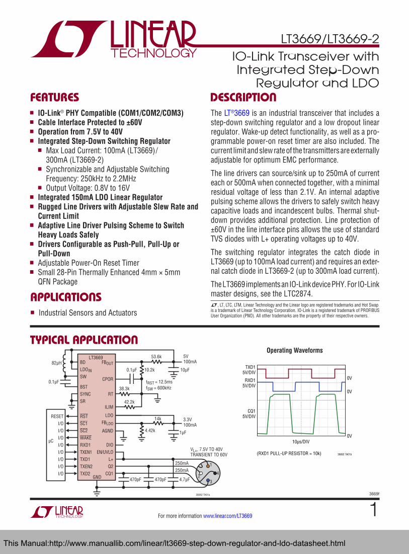
n IO-Link® PHY Compatible (COM1/COM2/COM3)n Cable Interface Protected to ±60Vn Operation from 7.5V to 40Vn Integrated Step-Down Switching Regulator
n Max Load Current: 100mA (LT3669)/ 300mA (LT3669-2)
n Synchronizable and Adjustable Switching Frequency: 250kHz to 2.2MHz
n Output Voltage: 0.8V to 16Vn Integrated 150mA LDO Linear Regulatorn Rugged Line Drivers with Adjustable Slew Rate and
Current Limitn Adaptive Line Driver Pulsing Scheme to Switch
Heavy Loads Safelyn Drivers Configurable as Push-Pull, Pull-Up or
Pull-Downn Adjustable Power-On Reset Timern Small 28-Pin Thermally Enhanced 4mm × 5mm
QFN Package
Typical applicaTion
FeaTures DescripTion
IO-Link Transceiver with Integrated Step-Down
Regulator and LDO
The LT®3669 is an industrial transceiver that includes a step-down switching regulator and a low dropout linear regulator. Wake-up detect functionality, as well as a pro-grammable power-on reset timer are also included. The current limit and slew rate of the transmitters are externally adjustable for optimum EMC performance.
The line drivers can source/sink up to 250mA of current each or 500mA when connected together, with a minimal residual voltage of less than 2.1V. An internal adaptive pulsing scheme allows the drivers to safely switch heavy capacitive loads and incandescent bulbs. Thermal shut-down provides additional protection. Line protection of ±60V in the line interface pins allows the use of standard TVS diodes with L+ operating voltages up to 40V.
The switching regulator integrates the catch diode in LT3669 (up to 100mA load current) and requires an exter-nal catch diode in LT3669-2 (up to 300mA load current).
The LT3669 implements an IO-Link device PHY. For IO-Link master designs, see the LTC2874.
Operating Waveforms
applicaTionsn Industrial Sensors and Actuators
L, LT, LTC, LTM, Linear Technology and the Linear logo are registered trademarks and Hot Swap is a trademark of Linear Technology Corporation. IO-Link is a registered trademark of PROFIBUS User Organization (PNO). All other trademarks are the property of their respective owners.
RSTSC1SC2WAKERXD1TXEN1TXD1TXEN2TXD2
RESETI/OI/OI/OI/OI/OI/OI/OI/O
DIOEN/UVLO
L+Q2
CQ1
AGND
FBLDO
LDO
ILIM
36692 TA01a
µC
GND
BSTSYNCSR
BDLDOINSW
FBOUT
RT
CPOR
250mA250mA
23
1
4
0.1µF
5V100mA
10µF
3.3V100mA
VL+, 7.5V TO 40VTRANSIENT TO 60V
LT3669
1µF
tRST = 12.5msfSW = 600kHz
0.1µF
82µH
38.3k
42.2k
53.6k
14k
4.42k
470pF
10.2k
470pF 4.7µF
10µs/DIV
TXD15V/DIV
RXD15V/DIV
(RXD1 PULL-UP RESISTOR = 10k)
CQ15V/DIV
0V
0V
0V
36692 TA01b
This Manual:http://www.manuallib.com/linear/lt3669-step-down-regulator-and-ldo-datasheet.html
LT3669/LT3669-2
23669f
For more information www.linear.com/LT3669
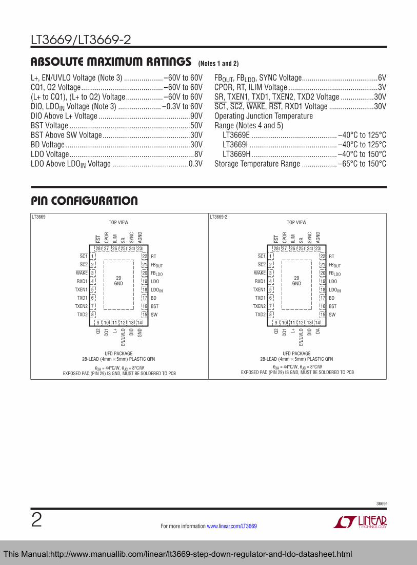
absoluTe MaxiMuM raTingsL+, EN/UVLO Voltage (Note 3) .................... –60V to 60VCQ1, Q2 Voltage .......................................... –60V to 60V(L+ to CQ1), (L+ to Q2) Voltage ................... –60V to 60V DIO, LDOIN Voltage (Note 3) ...................... –0.3V to 60VDIO Above L+ Voltage ...............................................90VBST Voltage ..............................................................50VBST Above SW Voltage .............................................30VBD Voltage ................................................................30VLDO Voltage ................................................................8VLDO Above LDOIN Voltage .......................................0.3V
(Notes 1 and 2)
pin conFiguraTion
FBOUT, FBLDO, SYNC Voltage .......................................6VCPOR, RT, ILIM Voltage ..............................................3VSR, TXEN1, TXD1, TXEN2, TXD2 Voltage .................30VSC1, SC2, WAKE, RST, RXD1 Voltage .......................30VOperating Junction Temperature Range (Notes 4 and 5) LT3669E ............................................ –40°C to 125°C LT3669I ............................................. –40°C to 125°C LT3669H ............................................ –40°C to 150°CStorage Temperature Range .................. –65°C to 150°C
LT3669 LT3669-2
9 10
TOP VIEW
UFD PACKAGE28-LEAD (4mm × 5mm) PLASTIC QFN
29GND
11 12 13
28 27 26 25 24
14
23
6
5
4
3
2
1SC1
SC2
WAKE
RXD1
TXEN1
TXD1
TXEN2
TXD2
RT
FBOUT
FBLDO
LDO
LDOIN
BD
BST
SW
RST
CPOR
ILIM
SR SYNC
AGND
Q2 CQ1 L+
EN/U
VLO
DIO
GND
7
17
18
19
20
21
22
16
8 15
θJA = 44°C/W, θJC = 8°C/W
EXPOSED PAD (PIN 29) IS GND, MUST BE SOLDERED TO PCB
9 10
TOP VIEW
UFD PACKAGE28-LEAD (4mm × 5mm) PLASTIC QFN
29GND
11 12 13
28 27 26 25 24
14
23
6
5
4
3
2
1SC1
SC2
WAKE
RXD1
TXEN1
TXD1
TXEN2
TXD2
RT
FBOUT
FBLDO
LDO
LDOIN
BD
BST
SW
RST
CPOR
ILIM
SR SYNC
AGND
Q2 CQ1 L+
EN/U
VLO
DIO DA
7
17
18
19
20
21
22
16
8 15
θJA = 44°C/W, θJC = 8°C/W
EXPOSED PAD (PIN 29) IS GND, MUST BE SOLDERED TO PCB
This Manual:http://www.manuallib.com/linear/lt3669-step-down-regulator-and-ldo-datasheet.html
LT3669/LT3669-2
33669f
For more information www.linear.com/LT3669
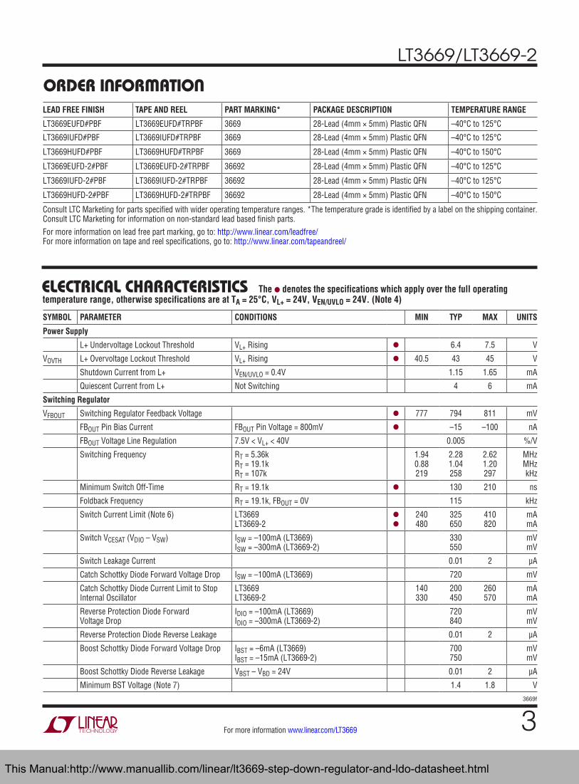
elecTrical characTerisTics The l denotes the specifications which apply over the full operating temperature range, otherwise specifications are at TA = 25°C, VL+ = 24V, VEN/UVLO = 24V. (Note 4)
SYMBOL PARAMETER CONDITIONS MIN TYP MAX UNITS
Power Supply
L+ Undervoltage Lockout Threshold VL+ Rising l 6.4 7.5 V
VOVTH L+ Overvoltage Lockout Threshold VL+ Rising l 40.5 43 45 V
Shutdown Current from L+ VEN/UVLO = 0.4V 1.15 1.65 mA
Quiescent Current from L+ Not Switching 4 6 mA
Switching Regulator
VFBOUT Switching Regulator Feedback Voltage l 777 794 811 mV
FBOUT Pin Bias Current FBOUT Pin Voltage = 800mV l –15 –100 nA
FBOUT Voltage Line Regulation 7.5V < VL+ < 40V 0.005 %/V
Switching Frequency RT = 5.36k RT = 19.1k RT = 107k
1.94 0.88 219
2.28 1.04 258
2.62 1.20 297
MHz MHz kHz
Minimum Switch Off-Time RT = 19.1k l 130 210 ns
Foldback Frequency RT = 19.1k, FBOUT = 0V 115 kHz
Switch Current Limit (Note 6) LT3669 LT3669-2
l
l
240 480
325 650
410 820
mA mA
Switch VCESAT (VDIO – VSW) ISW = –100mA (LT3669) ISW = –300mA (LT3669-2)
330 550
mV mV
Switch Leakage Current 0.01 2 µA
Catch Schottky Diode Forward Voltage Drop ISW = –100mA (LT3669) 720 mV
Catch Schottky Diode Current Limit to Stop Internal Oscillator
LT3669 LT3669-2
140 330
200 450
260 570
mA mA
Reverse Protection Diode Forward Voltage Drop
IDIO = –100mA (LT3669) IDIO = –300mA (LT3669-2)
720 840
mV mV
Reverse Protection Diode Reverse Leakage 0.01 2 µA
Boost Schottky Diode Forward Voltage Drop IBST = –6mA (LT3669) IBST = –15mA (LT3669-2)
700 750
mV mV
Boost Schottky Diode Reverse Leakage VBST – VBD = 24V 0.01 2 µA
Minimum BST Voltage (Note 7) 1.4 1.8 V
orDer inForMaTionLEAD FREE FINISH TAPE AND REEL PART MARKING* PACKAGE DESCRIPTION TEMPERATURE RANGE
LT3669EUFD#PBF LT3669EUFD#TRPBF 3669 28-Lead (4mm × 5mm) Plastic QFN –40°C to 125°C
LT3669IUFD#PBF LT3669IUFD#TRPBF 3669 28-Lead (4mm × 5mm) Plastic QFN –40°C to 125°C
LT3669HUFD#PBF LT3669HUFD#TRPBF 3669 28-Lead (4mm × 5mm) Plastic QFN –40°C to 150°C
LT3669EUFD-2#PBF LT3669EUFD-2#TRPBF 36692 28-Lead (4mm × 5mm) Plastic QFN –40°C to 125°C
LT3669IUFD-2#PBF LT3669IUFD-2#TRPBF 36692 28-Lead (4mm × 5mm) Plastic QFN –40°C to 125°C
LT3669HUFD-2#PBF LT3669HUFD-2#TRPBF 36692 28-Lead (4mm × 5mm) Plastic QFN –40°C to 150°C
Consult LTC Marketing for parts specified with wider operating temperature ranges. *The temperature grade is identified by a label on the shipping container.Consult LTC Marketing for information on non-standard lead based finish parts.For more information on lead free part marking, go to: http://www.linear.com/leadfree/ For more information on tape and reel specifications, go to: http://www.linear.com/tapeandreel/
This Manual:http://www.manuallib.com/linear/lt3669-step-down-regulator-and-ldo-datasheet.html
LT3669/LT3669-2
43669f
For more information www.linear.com/LT3669
SYMBOL PARAMETER CONDITIONS MIN TYP MAX UNITS
BST Pin Current ISW = –100mA (LT3669) ISW = –300mA (LT3669-2)
5.25 10.5
7.5 15
mA mA
SYNC Threshold Voltage 0.5 0.9 1.5 V
SYNC Input Frequency 0.3 2.2 MHz
EN/UVLO Threshold Voltage VEN/UVLO Rising l 1.44 1.5 1.56 V
EN/UVLO Pin Hysteresis l 50 75 100 mV
LDO Linear Regulator
VFBLDO LDO Feedback Voltage l 777 794 811 mV
FBLDO Pin Bias Current FBLDO Pin Voltage = 800mV l –20 –100 nA
FBLDO Voltage Line Regulation 7.5V < VL+ < 40V, VL+ – VLDO > 4V 0.005 %/V
LDO Current Limit l 151 180 235 mA
LDO Current Limit Foldback VLDOIN = 40V, VLDO = 0V l 15 35 55 mA
LDO Dropout Voltage LDO Load Current = 25mA LDO Load Current = 150mA
l 60 340
90 mV mV
LDO Minimum Load Current l 150 175 µA
Power-On Reset
VRSTTH Reset Threshold as % of VFBOUT (VFBLDO) FBOUT (FBLDO) Pin Voltage Falling (Figure 6) l 90.4 92.7 95 %
tRST Reset Timeout Period CPOR = 100nF, RST RPU = 100k (Figure 6) l 10 12.5 15 ms
tUV UV Detect to RST Asserted Step VFBOUT (VFBLDO) from 0.9V to 0.5V, RST RPU = 100k (Figure 6)
l 11 24 37 µs
Line Driver Thermal Shutdown
Thermal Shutdown Threshold (Note 8) Junction Temperature TJ Increasing 125 140 155 °C
Thermal Shutdown Threshold (Note 8) Junction Temperature TJ Decreasing 111 128 135 °C
Thermal Shutdown Hysteresis (Note 8) 10 12 14 °C
Line Drivers
IQH DC Driver Current P-Switching Output (ON State)
VILIM ≤ 0.3V, 7.5V < VL+ < 40V RILIM = 42.2k, 7.5V < VL+ < 40V
l
l
105 280
140 330
190 420
mA mA
IQL DC Driver Current N-Switching Output (ON State)
VILIM ≤ 0.3V, 7.5V < VL+ < 40V RILIM = 42.2k, 7.5V < VL+ < 40V
l
l
105 280
140 330
190 420
mA mA
VRQH Residual Voltage High (VL+ to VCQ1,Q2) ICQ1,Q2 = –100mA ICQ1,Q2 = –250mA
l
l
1.15 1.5
1.65 2.1
V V
VRQL Residual Voltage Low (VCQ1,Q2) ICQ1,Q2 = 100mA ICQ1,Q2 = 250mA
l
l
1.15 1.5
1.65 2.1
V V
VRQH (VRQL) Pulsing Threshold VRQH (VRQL) Increasing 2.7 2.95 3.2 V
VRQH (VRQL) Pulsing Threshold Hysteresis 20 50 80 mV
CQ1, Q2 Pin Leakage Current –40°C to 125°C, VTXENn < 0.4V –40°C to 150°C, VTXENn < 0.4V
l
l
±1.2 ±1.2
±3 ±8
µA µA
Receiver
VTHH Input Threshold “H” VL+ > 18V (Figure 14) l 10.5 11.8 13 V
VTHL Input Threshold “L” VL+ > 18V (Figure 14) l 8.0 9.6 11.2 V
VHYS Input Hysteresis VL+ > 18V (Figure 14) l 1.8 2.2 2.6 V
elecTrical characTerisTics The l denotes the specifications which apply over the full operating temperature range, otherwise specifications are at TA = 25°C, VL+ = 24V, VEN/UVLO = 24V. (Note 4)
This Manual:http://www.manuallib.com/linear/lt3669-step-down-regulator-and-ldo-datasheet.html
LT3669/LT3669-2
53669f
For more information www.linear.com/LT3669
The l denotes the specifications which apply over the full operating temperature range, otherwise specifications are at TA = 25°C, VL+ = 24V, VEN/UVLO = 24V. (Note 4)elecTrical characTerisTics
swiTching characTerisTics The l denotes the specifications which apply over the full operating temperature range, otherwise specifications are at TA = 25°C, VL+ = 24V, VEN/UVLO = 24V. (Note 4)SYMBOL PARAMETER CONDITIONS MIN TYP MAX UNITS
Driver and Receiver
fDTR Maximum Data Transfer Rate CCQ1,Q2 ≤ 4nF VSR ≤ 0.4V (for COM1/COM2) VSR ≥ 0.9V (for COM3)
l
l
38.4
230.4
kb/s kb/s
tBIT Bit Time VSR ≤ 0.4V (for COM2) VSR ≥ 0.9V (for COM3)
26.04 4.34
µs µs
Driver
tDR Rise Time CCQ1,Q2 ≤ 4nF (Figure 1) VSR ≤ 0.4V (for COM1/COM2) VSR ≥ 0.9V (for COM3)
l
l
1.6
0.26
5.2
0.869
µs µs
tDF Fall Time CCQ1,Q2 ≤ 4nF (Figure 1) VSR ≤ 0.4V (for COM1/COM2) VSR ≥ 0.9V (for COM3)
l
l
2.1
0.34
5.2
0.869
µs µs
tPHLD, tPLHD Propagation Delay CCQ1,Q2 ≤ 4nF (Figure 2) VSR ≤ 0.4V (for COM1/COM2) VSR ≥ 0.9V (for COM3)
l
l
3.3
0.72
6
1.3
µs µs
tSKEWD Skew tSKEWD = |tPHLD – tPLHD|, CCQ1,Q2 ≤ 4nF (Figure 2) VSR ≤ 0.4V (for COM1/COM2) VSR ≥ 0.9V (for COM3)
l
l
0.25 140
1.5 400
µs ns
tZHD, tZLD Enable Time CCQ1,Q2 = 100pF, RPU = RPD = 10k (Figure 3) VSR ≤ 0.4V (for COM1/COM2) VSR ≥ 0.9V (for COM3)
l
l
3.4 0.8
6.1 1.4
µs µs
tHZD, tLZD Disable Time CCQ1,Q2 = 100pF, RPU = RPD = 10k (Figure 3) VSR ≤ 0.4V (for COM1/COM2) VSR ≥ 0.9V (for COM3)
l
l
4 4
6 6
µs µs
tDWU Minimum Wake-Up Pulse Duration to Be Acknowledged
RPU = RPD = 10k (Figure 7) WAKE Pull-Up Resistor = 5k
l 55 75 µs
tLZW Delay From Handshake Sequence Finished to WAKE High (Note 9)
WAKE Pull-Up Resistor = 5k 0.3 1 µs
Pulsing On-Time VRQH (VRQL) = 24V, Only CQ1 or Q2 Pulsing 320 µs
Pulsing Off-Time 2.2 ms
SYMBOL PARAMETER CONDITIONS MIN TYP MAX UNITS
Digital IO
WAKE, RXD1, SCn Pull-Down Output Current if Asserted
VSCn = VWAKE = VRXD1 = 0.3V l 0.7 1.05 mA
RST Pull-Down Output Current if Asserted VRST = 0.3V l 0.2 0.3 mA
VIH TXDn, TXENn, SR Input High Voltage l 0.9 V
VIL TXDn, TXENn, SR Input Low Voltage l 0.4 V
ILK TXDn, TXENn, SR Pin Input Leakage Current 0.1 1 µA
CIN TXDn, TXENn, SR Pin Input Capacitance 2.5 pF
This Manual:http://www.manuallib.com/linear/lt3669-step-down-regulator-and-ldo-datasheet.html
LT3669/LT3669-2
63669f
For more information www.linear.com/LT3669
The l denotes the specifications which apply over the full operating temperature range, otherwise specifications are at TA = 25°C, VL+ = 24V, VEN/UVLO = 24V. (Note 4)
Note 1: Stresses beyond those listed under Absolute Maximum Ratings may cause permanent damage to the device. Exposure to any Absolute Maximum Rating condition for extended periods may affect device reliability and lifetime.Note 2: All voltages are with respect to GND. All currents into device pins are positive; all currents out of device pins are negative.Note 3: Absolute maximum voltage at L+, EN/UVLO, DIO and LDOIN pins is 60V for non-repetitive one second transients, and 40V for continuous operation.Note 4: The LT3669E is guaranteed to meet performance specifications from 0°C to 125°C junction temperature. Specifications over the –40°C to 125°C operating junction temperature range are assured by design, characterization and correlation with statistical process controls. The LT3669I is guaranteed over the full –40°C to 125°C operating junction temperature range. The LT3669H is guaranteed over the full –40°C to 150°C operating junction temperature range. Specifications for the line driver do not apply above the thermal shutdown temperature.
Note 5: This IC includes overtemperature protection that is intended to protect the device during momentary overload conditions and will shut the line drivers off for typical junction temperatures higher than 140°C. The LDO and switching regulator will shut off for typical junction temperatures higher than 168°C. Continuous operation above the specified maximum operating junction temperature may impair device reliability.Note 6: Current limit guaranteed by design and/or correlation to static test. Slope compensation reduces current limit at higher duty cycles.Note 7: This is the minimum voltage across the boost capacitor needed to guarantee full saturation of the NPN power switch.Note 8: Thermal shutdown guaranteed by design and/or correlation to static test.Note 9: Handshake sequence: set TXEN1 low and then toggle TXD1.
swiTching characTerisTics
SYMBOL PARAMETER CONDITIONS MIN TYP MAX UNITS
Receiver
Noise Suppression Time VSR ≤ 0.4V (for COM1/COM2) (Figure 5) VSR ≥ 0.9V (for COM3) (Figure 5)
l
l
1/16 1/16
3.5/16 5/16
TBIT TBIT
tPHLR, tPLHR Propagation Delay RXD1 Pull-Up Resistor = 5k (Figure 4) VSR ≤ 0.4V (for COM1/COM2) VSR ≥ 0.9V (for COM3)
l
l
4.6
1.45
6.5 2.1
µs µs
tSKEWR Receiver Skew tSKEWR = |tPHLR – tPLHR|, RXD1 RPU = 5k (Figure 4) VSR ≤ 0.4V (for COM1/COM2) VSR ≥ 0.9V (for COM3)
l
l
0.5 100
1.5 400
µs ns
CCQI CQ1 Pin Input Capacitance 20 pF
This Manual:http://www.manuallib.com/linear/lt3669-step-down-regulator-and-ldo-datasheet.html
LT3669/LT3669-2
73669f
For more information www.linear.com/LT3669
TEMPERATURE (°C)–50 0 50 75–25 25 125100 150
36692 G02
FEED
BACK
VOL
TAGE
(mV)
780
800
790
785
805
795
810
TEMPERATURE (°C)
FEED
BACK
VOL
TAGE
(mV)
780
800
790
785
805
795
810
36692 G01
–50 0 50 75–25 25 125100 150
TEMPERATURE (°C)–50
OVLO
(V)
0 50 7541.0
43.0
42.0
41.5
43.5
42.5
44.5
44.0
–25 25 125100 150
36692 G04
VL+ RISING
VL+ FALLING
TEMPERATURE (°C)–50
EN/U
VLO
PIN
THRE
SHOL
D (V
)
0 50 751.30
1.50
1.40
1.35
1.55
1.45
1.60
–25 25 125100 150
36692 G03
EN/UVLO RISING
EN/UVLO FALLINGUV
LO (V
)
5.0
6.0
7.0
5.5
6.5
7.5
TEMPERATURE (°C)–50 0 50 75–25 25 125100 150
36692 G05
VL+ RISING
VL+ FALLING
0
L+ S
UPPL
Y CU
RREN
T (m
A)
10 150
0.8
0.4
0.2
1.0
0.6
1.4
1.2
5 2520 30 35 40
36692 G06VL+ (V)
VL+ = 24V
0
L+ S
UPPL
Y CU
RREN
T (m
A)
0.4
0.8
1.2
1.4
0.2
0.6
1.0
TEMPERATURE (°C)36692 G07
–50 0 50 75–25 25 125100 150
Typical perForMance characTerisTics
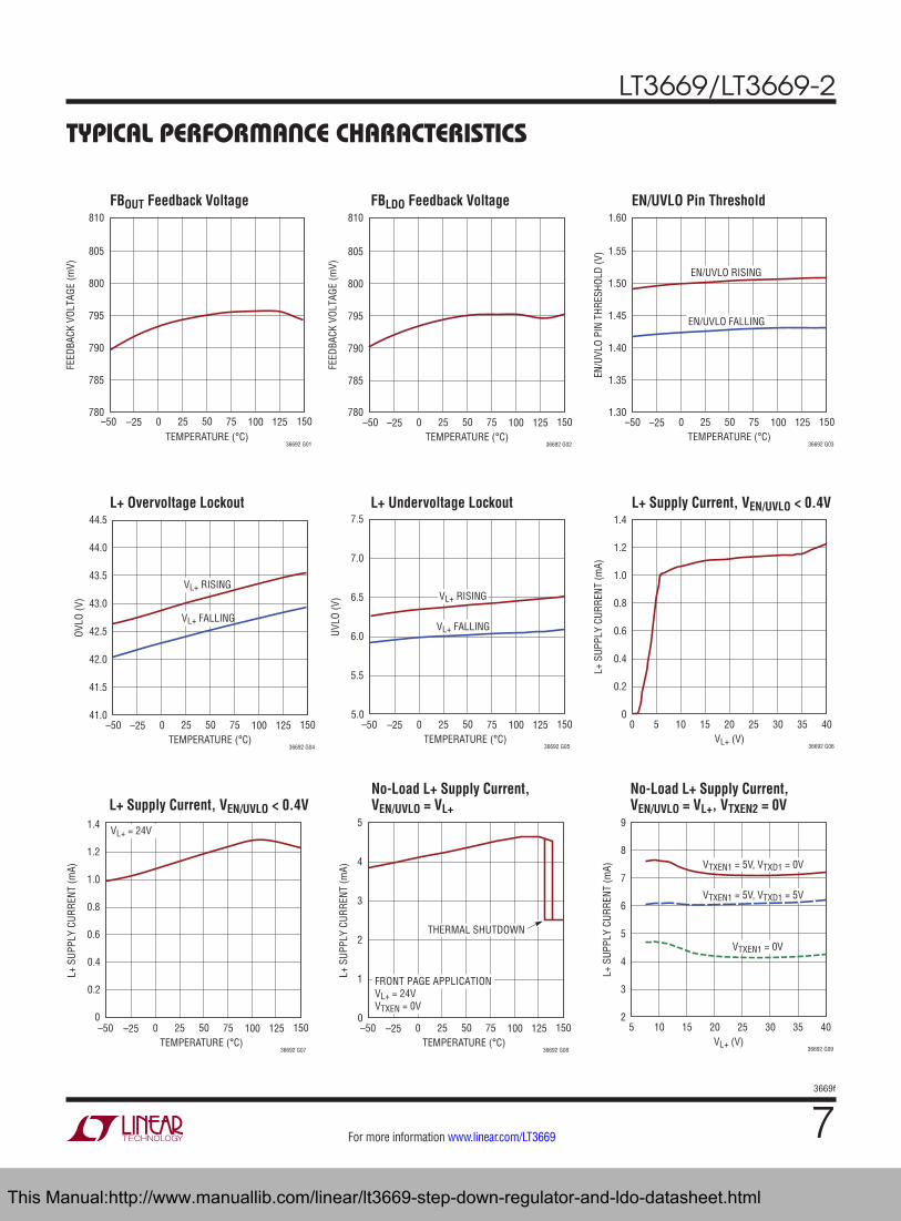
L+ Overvoltage Lockout L+ Undervoltage Lockout L+ Supply Current, VEN/UVLO < 0.4V
L+ Supply Current, VEN/UVLO < 0.4VNo-Load L+ Supply Current, VEN/UVLO = VL+
No-Load L+ Supply Current, VEN/UVLO = VL+, VTXEN2 = 0V
FBOUT Feedback Voltage FBLDO Feedback Voltage EN/UVLO Pin Threshold
L+ S
UPPL
Y CU
RREN
T (m
A)
0
2
4
1
3
5
TEMPERATURE (°C)36692 G08
THERMAL SHUTDOWN
FRONT PAGE APPLICATIONVL+ = 24VVTXEN = 0V
–50 0 50 75–25 25 125100 150
L+ S
UPPL
Y CU
RREN
T (m
A)
10 152
6
4
3
7
5
9
8
5 2520 30 35 40
36692 G09VL+ (V)
VTXEN1 = 5V, VTXD1 = 0V
VTXEN1 = 5V, VTXD1 = 5V
VTXEN1 = 0V
This Manual:http://www.manuallib.com/linear/lt3669-step-down-regulator-and-ldo-datasheet.html
LT3669/LT3669-2
83669f
For more information www.linear.com/LT3669
0
SWIT
CH V
OLTA
GE D
ROP,
VCE
SAT
(mV)
100 150
300
100
0
400
200
350
150
50
250
450
50 250200 300
36692 G15SWITCH CURRENT (mA)
12.0
RESE
T TI
MEO
UT P
ERIO
D, t R
ST (m
s)12.4
12.6
12.8
13.0
12.3
12.2
12.1
12.5
12.7
12.9
TEMPERATURE (°C)36692 G11
CPOR = 100nF
–50 0 50 75–25 25 125100 150CPOR PIN CAPACITANCE, CPOR (nF)
RESE
T TI
MEO
UT P
ERIO
D, t R
ST (m
s)
0.1 1 10 100 1000 100000.01
0.1
1
100
10
0.01
1000
36692 G12
DUTY CYCLE (%)0
SWIT
CH C
URRE
NT L
IMIT
(mA)
400
500
600
70
300
200
20 4010 9030 50 8060 100
100
0
700
36692 G13
LT3669-2
LT3669
0
BST
PIN
CURR
ENT
(mA)
100 150
6
2
0
8
4
7
3
1
9
5
10
50 250200 300
36692 G16SWITCH CURRENT (mA)
Typical perForMance characTerisTics
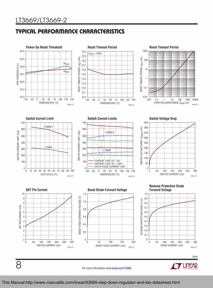
Switch Current Limit Switch Current Limits Switch Voltage Drop
BST Pin Current Boost Diode Forward VoltageReverse-Protection Diode Forward Voltage
Power-On Reset Threshold Reset Timeout Period Reset Timeout Period
TEMPERATURE (°C)
POR
THRE
SHOL
D (%
)
91.0
93.0
92.0
91.5
93.5
92.5
94.O
36692 G10
FBOUT
FBLDO
–50 0 50 75–25 25 125100 150
400
500
600
300
200
100
0
700
SWIT
CH C
URRE
NT L
IMIT
(mA)
TEMPERATURE (°C)36692 G14
CURRENT LIMIT DC = 0%CURRENT LIMIT DC = 100%CATCH DIODE CURRENT LIMIT
LT3669-2
LT3669
–50 0 50 75–25 25 125100 150
BOOST DIODE CURRENT (mA)0
0.8
1.0
0.6
0.4
10050 150 200
0.2
0
1.2
BOOS
T DI
ODE
FORW
ARD
VOLT
AGE
(V)
36692 G17DIODE CURRENT (mA)
00
REVE
RSE-
PROT
ECTI
ON D
IODE
VF
(V)
0.2
0.4
0.6
50 100 150 200 250
0.8
1.0
0.1
0.3
0.5
0.7
0.9
300
36692 G18
This Manual:http://www.manuallib.com/linear/lt3669-step-down-regulator-and-ldo-datasheet.html
LT3669/LT3669-2
93669f
For more information www.linear.com/LT3669
VL+ = 24VRT = 38.3kΩ
FREQ
UENC
Y (k
Hz)
580
600
620
570
590
610
630
TEMPERATURE (°C)36692 G19
–50 0 50 75–25 25 125100 150 0
SWIT
CHIN
G FR
EQUE
NCY
(kHz
)
40 60
1400
600
200
1800
1000
1600
800
400
2000
1200
2200
20 10080 120
36692 G20RT (kΩ)
BUCK
LOA
D CU
RREN
T (m
A)
300
100
0
400
200
350
150
50
450
250
500
36692 G23
5 15 2010 30 3525 40VL+ (V)
TYPICALMINIMUM
LT3669-2, L = 33µH
LT3669, L = 82µH
f = 600kHzDIO PIN FLOATING
0
EFFI
CIEN
CY (%
)
100 150
75
35
15
55
85
45
25
65
95
50 250200 300
36692 G24BUCK LOAD CURRENT (mA)
ALL LT3669 CURRENT INCLUDEDf = 600kHz, VTXEN = 0V, VILIM = 0VDIO PIN FLOATING
12V24V36V
LT3669 VL+ :12V24V36V
LT3669-2 VL+ :
0
EFFI
CIEN
CY (%
)
100 150
70
30
10
50
80
40
20
60
90
50 250200 300
36692 G27BUCK LOAD CURRENT (mA)
ALL LT3669 CURRENT INCLUDEDf = 400kHz, VTXEN = 0V, VILIM = 0VDIO PIN FLOATING
12V24V36V
LT3669 VL+ :12V24V36V
LT3669-2 VL+ :
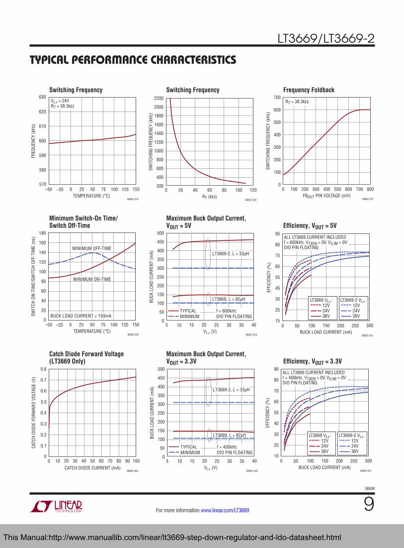
Typical perForMance characTerisTics
Minimum Switch-On Time/ Switch Off-Time
Maximum Buck Output Current, VOUT = 5V Efficiency, VOUT = 5V
Catch Diode Forward Voltage (LT3669 Only)
Maximum Buck Output Current, VOUT = 3.3V Efficiency, VOUT = 3.3V
Switching Frequency Switching Frequency Frequency Foldback
0
SWIT
CHIN
G FR
EQUE
NCY
(kHz
)
200 3000
400
200
100
500
300
700
600
100 500400 600 700 800
36692 G21FBOUT PIN VOLTAGE (mV)
RT = 38.3kΩ
SWIT
CH O
N-T
IME/
SWIT
CH O
FF-T
IME
(ns)
TEMPERATURE (°C)–50 0 50 75–25 25 125100 150
36692 G22
MINIMUM OFF-TIME
MINIMUM ON-TIME
BUCK LOAD CURRENT = 150mA
120
40
0
160
80
140
60
20
100
180
BUCK
LOA
D CU
RREN
T (m
A)
300
100
0
400
200
350
150
50
450
250
500
36692 G25
5 15 2010 30 3525 40VL+ (V)
TYPICALMINIMUM
LT3669-2, L = 33µH
LT3669, L = 82µH
f = 400kHzDIO PIN FLOATING
CATCH DIODE CURRENT (mA)0
CATC
H DI
ODE
FORW
ARD
VOLT
AGE
(V)
0.4
0.5
0.7
0.6
70
0.3
0.2
20 4010 9030 50 8060 100
0.1
0
0.8
36692 G25
This Manual:http://www.manuallib.com/linear/lt3669-step-down-regulator-and-ldo-datasheet.html
LT3669/LT3669-2
103669f
For more information www.linear.com/LT3669
0
DROP
OUT
VOLT
AGE,
VLD
OIN
– V L
DO (m
V)
100
200
300
400
50
150
250
350 ILOAD = 150mA
ILOAD = 30mA
TEMPERATURE (°C)–50 0 50 75–25 25 125100 150
36692 G30
LDO
CURR
ENT
LIM
IT (m
A)
VL+ = 24V
TEMPERATURE (°C)36692 G31
140
60
20
180
100
160
80
40
220
200
120
VLDOIN – VLDO = 5V
VLDOIN – VLDO = 24V
VLDOIN – VLDO = 30V
VLDOIN – VLDO = 40V
–50 0 50 75–25 25 125100 150 0
LDO
CURR
ENT
LIM
IT (m
A)
10 15
140
60
20
180
100
160
80
40
200
120
5 25 30 3520 40
36692 G32VLDOIN – VLDO (V)
TEMPERATURE (°C)–50
LDO
MIN
IMUM
LOA
D CU
RREN
T (µ
A)
0 50 75100
150
350
250
200
400
300
450
–25 25 125100 150
36692 G33
VLDO = 300mVVLDO = 400mVVLDO = 500mVVLDO = 600mVVLDO = 700mV
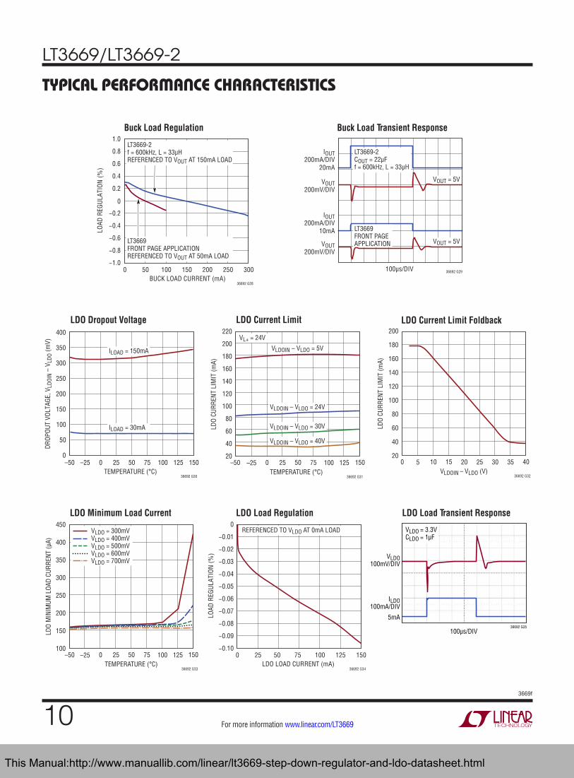
Typical perForMance characTerisTics
LDO Current Limit Foldback
LDO Minimum Load Current LDO Load Regulation LDO Load Transient Response
LDO Dropout Voltage
Buck Load Regulation Buck Load Transient Response
LDO Current Limit
100µs/DIV
VLDO100mV/DIV
ILDO100mA/DIV
5mA36692 G35
VLDO = 3.3VCLDO = 1µF
0
36692 G28
−1.0
−0.8
−0.6
−0.4
−0.2
0.2
0.4
0.6
0.8
1.0
LOAD
REG
ULA
TIO
N (%
)
0 50 100 150 200 250 300BUCK LOAD CURRENT (mA)
LT3669FRONT PAGE APPLICATIONREFERENCED TO VOUT AT 50mA LOAD
LT3669-2f = 600kHz, L = 33µHREFERENCED TO VOUT AT 150mA LOAD
36692 G29
VOUT = 5V
VOUT = 5V
IOUT200mA/DIV
20mA
VOUT200mV/DIV
IOUT200mA/DIV
10mA
VOUT200mV/DIV
100µs/DIV
LT3669-2COUT = 22µFf = 600kHz, L = 33µH
LT3669FRONT PAGEAPPLICATION
36692 G34
LOAD
REG
ULA
TIO
N (%
)
0 25 50 75 100 125 150LDO LOAD CURRENT (mA)
REFERENCED TO VLDO AT 0mA LOAD
−0.10
−0.09
−0.08
−0.07
−0.06
−0.05
−0.04
−0.03
−0.02
−0.01
0
This Manual:http://www.manuallib.com/linear/lt3669-step-down-regulator-and-ldo-datasheet.html
LT3669/LT3669-2
113669f
For more information www.linear.com/LT3669
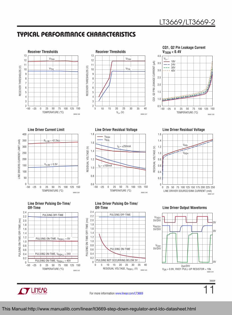
Typical perForMance characTerisTics
Line Driver Current Limit
CQ1, Q2 Pin Leakage Current VTXEN < 0.4V
Line Driver Pulsing On-Time/Off-Time
Line Driver Pulsing On-Time/Off-Time Line Driver Output Waveforms
Line Driver Residual Voltage Line Driver Residual Voltage
Receiver Thresholds Receiver Thresholds
TEMPERATURE (°C)–50
RECE
IVER
THR
ESHO
LDS
(V)
0 50 752
6
4
10
12
8
3
7
5
11
13
9
–25 25 125100 150
36692 G36
VTHH
VTHL
5
RECE
IVER
THR
ESHO
LDS
(V)
15 25 302
6
4
10
12
8
3
7
5
11
13
9
10 20 35 40
36692 G37
VTHH
VTHL
VL+ (V) TEMPERATURE (°C)–50
CQ1,
Q2
PIN
LEAK
AGE
CURR
ENT
(µA)
0 50 750.5
1.0
3.0
2.0
1.5
3.5
2.5
4.0
–25 25 125100 150
36692 G38
18V24V30V40V
VL+ :
0
LINE
DRI
VERS
CUR
RENT
LIM
IT (m
A)
100
200
300
400
50
150
250
350 RILIM = 42.2kΩ
VILIM ≤ 0.3V
TEMPERATURE (°C)–50 0 50 75–25 25 125100 150
36692 G39TEMPERATURE (°C)
–50
RESI
DUAL
VOL
TAGE
(V)
0 50 750.6
1.4
1.0
0.8
1.6
1.2
1.8
–25 25 125100 150
36692 G40
VRQHVRQL
IQ = ±250mA
IQ = ±100mA
36692 G41
VRQL
VRQH
0 25 50 75 100 125 150 175 200 225 250LINE DRIVER SOURCE/SINK CURRENT (mA)
0
0.2
0.4
0.6
0.8
1.0
1.2
1.4
1.6
RES
IDU
AL V
OLT
AGE
(V)
TEMPERATURE (°C)36692 G42
PULSING ON-TIME, VRQH,L = 40V
PULSING ON-TIME, VRQH,L = 24V
PULSING ON-TIME, VRQH,L = 5V
PULSING OFF-TIME
0
0.2
0.4
0.6
0.8
1.0
1.2
1.4
1.6
1.8
2.0
2.2
2.4
PULS
ING
ON
-TIM
E/O
FF-T
IME
(ms)
–50 0 50 75–25 25 125100 150 0 10 20 25 405 15 30 35RESIDUAL VOLTAGE, VRQH,L (V)
36692 G43
PULSING NOT OCCURRING BELOW 3V
PULSING ON-TIME
PULSING OFF-TIME
0
0.2
0.4
0.6
0.8
1.0
1.2
1.4
1.6
1.8
2.0
2.2
2.4
PULS
ING
ON
-TIM
E/O
FF-T
IME
(ms)
36692 G44
0V
0V
0V
VTXD15V/DIV
VRXTD15V/DIV
VCQ15V/DIV
VSR > 0.9V, RXD1 PULL-UP RESISTOR = 10k2µs/DIV
This Manual:http://www.manuallib.com/linear/lt3669-step-down-regulator-and-ldo-datasheet.html
LT3669/LT3669-2
123669f
For more information www.linear.com/LT3669
pin FuncTionsSC1 (Pin 1): CQ1 Short-Circuit Detect Open-Collector Output. SC1 pulls low when a short-circuit is detected on the CQ1 driver output or after a thermal shutdown event. Use a 100k pull-up resistor to the µC’s supply. Lowpass filter this signal before further processing. See the Ap-plications Information section.
SC2 (Pin 2): Q2 Short-Circuit Detect Open-Collector Output. SC2 pulls low when a short-circuit is detected on the Q2 driver output or after a thermal shutdown event. Use a 100k pull-up resistor to the µC’s supply. Lowpass filter this signal before further processing. See the Ap-plications Information section.
WAKE (Pin 3): Wake-up Detect Open-Collector Output. WAKE pulls low when driver 1 detects a wake-up pulse longer than 75µs at the CQ1 pin (indicating that a data transmission is beginning). WAKE returns to high imped-ance after the handshaking sequence of setting TXEN1 low and then toggling TXD1 or after an internal reset event. Use a 10k pull-up resistor to the µC’s supply.
RXD1 (Pin 4): CQ1 Receiver Output, Open Collector. Use a pull-up resistor of 10k or less for improved data perfor-mance in COM3. RXD1 polarity is inverted with respect to the line data CQ1.
TXEN1 (Pin 5): CQ1 Driver Enable. The TXEN1 pin enables the line data CQ1 driver in push-pull mode when pulled high. To use the driver in open-collector mode, tie TXD1 high (for pull-down mode) or low (for pull-up mode) and drive the data signal into the TXEN1 pin.
TXD1 (Pin 6): CQ1 Driver Input. The polarity of the driver output is inverted with respect to TXD1.
TXEN2 (Pin 7): Q2 Driver Enable. The TXEN2 pin enables the line data Q2 driver in push-pull mode when pulled high. To use the driver in open-collector mode, tie TXD2 high (for pull-down mode) or low (for pull-up mode) and drive the data signal into the TXEN2 pin.
TXD2 (Pin 8): Q2 Driver Input. The polarity of the driver output is inverted with respect to TXD2.
Q2 (Pin 9): Q2 Driver Output. The driver output polarity is inverted with respect to the driver input TXD2. Con-nect a capacitor (typically 470pF) from Q2 to ground for improved performance.
CQ1 (Pin 10): CQ1 Driver Output and Receiver Input. The driver output polarity is inverted with respect to the driver input TXD1. Tie directly to the industrial line data terminal. Connect a capacitor (typically 470pF) from CQ1 to ground for improved performance.
L+ (Pin 11): Power Supply Input and Anode of Internal Reverse Polarity Protection Diode. Connect to the industrial line supply terminal. The L+ pin supplies current to the LT3669’s internal circuitry and must be locally bypassed with at least 4.7µF.
EN/UVLO (Pin 12): The EN/UVLO pin puts the LT3669 in shutdown mode. Pull the pin below 0.4V to shut down the LT3669. The 1.5V threshold functions as an accurate undervoltage lockout (UVLO), preventing the regulators and transceiver from operating until the input voltage has reached the programmed level.
DIO (Pin 13): Cathode of Internal Reverse Polarity Pro-tection Diode. Do not use a bypass capacitor at DIO. An external diode from L+ to DIO can be used to improve efficiency. In this case only, a bypass capacitor is al-lowed at DIO. The external diode must be chosen with a reverse-breakdown voltage higher than the expected reverse-polarity condition, and it must be robust enough to withstand the inrush current of hot plugging.
GND (Pin 14, LT3669): Ground in LT3669. Leave this pin floating or tie the pin directly to the ground plane and the industrial line ground terminal L–.
DA (Pin 14, LT3669-2): Diode Anode in LT3669-2. Connect the anode of the external catch diode (D1 in LT3669-2's Block Diagram) to this pin. Internal circuitry senses the current through the catch diode providing frequency foldback in extreme situations.
SW (Pin 15): Output of the Internal NPN Power Switch. Connect this pin to the inductor and boost capacitor.
BST (Pin 16): The BST pin provides drive voltage higher than the input voltage to the internal NPN power switch. Connect a capacitor (typically 0.22µF) between BST and SW.
BD (Pin 17): An integrated Schottky diode is connected from BD to BST, providing the charging path for the boost capacitor. Connect to the output of the switching regulator.
This Manual:http://www.manuallib.com/linear/lt3669-step-down-regulator-and-ldo-datasheet.html
LT3669/LT3669-2
133669f
For more information www.linear.com/LT3669
LDOIN (Pin 18): LDO Power Supply Input. This is the collector of the LDO power NPN. Tie to the output of the switching regulator for maximum efficiency, or to DIO. To preserve reverse-polarity protection, do not connect to L+.
LDO (Pin 19): Low Dropout Linear Regulator Output. Bypass to GND with at least 1µF of capacitance.
FBLDO (Pin 20): The LT3669 regulates this pin to 0.794V. Connect a feedback resistor divider tap to this pin to set the output voltage of the LDO.
FBOUT (Pin 21): The LT3669 regulates this pin to 0.794V. Connect a feedback resistor divider tap to this pin to set the output voltage of the switching regulator.
RT (Pin 22): Sets the Internal Oscillator Frequency. Tie a resistor from RT to AGND to program the frequency. See Table 2 for resistor values.
AGND (Pin 23): Analog Ground Used for Bandgap Voltage References. Connect to the ground node of the passive components connected to RT, FBOUT, FBLDO, ILIM and CPOR, and to the system ground in a star connection manner.
SYNC (Pin 24): External Clock Synchronization Input. Ground this pin to run the part using the internal oscil-lator. For external synchronization, drive the SYNC pin with a logic-level signal with positive and negative pulse widths of at least 80ns. Choose the RT resistor to set the LT3669 switching frequency at least 20% below the lowest synchronization input. For example, if the synchronization signal is 350kHz, the RT pin should be set for 280kHz.
SR (Pin 25): Slew Rate Control Pin. Setting SR low ad-justs both CQ1 and Q2 drivers’ rising and falling times for reduced EMI in COM1/COM2 speed mode. Set SR high for edge times suitable for COM3.
ILIM (Pin 26): Line Driver Current Limit Programming Pin. Source and sink current limits for both line drivers are programmed using this pin. Tie a resistor from ILIM to AGND to set the drivers output current limit. Tie ILIM to AGND for a 140mA current limit.
CPOR (Pin 27): Reset Delay Timer Programming Pin. Connect an external capacitor (CPOR) to AGND to program a reset delay time of 0.125ms/nF.
RST (Pin 28): Active Low, Open-collector Logic Output. After VOUT and VLDO rises above 92.7% of its programmed value, the reset remains asserted for the period set by the capacitor on the CPOR pin. RST will also pull low if VL+ is below the internal undervoltage threshold and VOUT or VLDO are above 1.5V for an RST pull-up resistor of 100k. If using the POR function, connect a 10pF capacitor between the CPOR and RST pins.
GND (Pin 29 Exposed Pad): Ground. Tie the exposed pad directly to the ground plane and the industrial line ground terminal. The exposed pad metal of the package provides both electrical contact to ground and good thermal contact to the circuit printed board. It must be soldered to the circuit board for proper operation.
pin FuncTions
This Manual:http://www.manuallib.com/linear/lt3669-step-down-regulator-and-ldo-datasheet.html
LT3669/LT3669-2
143669f
For more information www.linear.com/LT3669
block DiagraM
L+
CQ1
THSD THSDRST
C/Q
Q2
Q2
Q
+–
+–
+–
+–
SC
WAKE
ENABLE
GND
AGND
3V
LDO
OSCILLATOR250kHz TO 2.2MHz
CATCHDIODE
BOOSTDIODE
SWITCHDRIVER
DISABLE
EN
EN
SYNC
+–
+–
+–
VC CLAMP
VC SOFT-START
1519
20
25
TXD16
26
TXEN27
TXD2
SR
ILIM
8
CPOR27
SLOPE COMP R
S
Q
QB
SW
24SYNC
L+
L–
9
22RT
12
21
EN/UVLO
13DIO
16BST
17BD
18LDOIN
L
COUT
VOUT
14GND
36692 BD1
CBST
RTR1
R2
0.794VFBOUT
FBLDO
FBLDO
R3
R4
LOW DROPOUT LINEAR REGULATOR
+–
ENABLE EN
RST
+–
0.794V
EN
CLDO
VLDO
CPOR
RST28
POWER-ONRESET
CONTROLREFERENCE GENERATOR
TEMPERATUREAND VOLTAGEMONITORING
0.736VFBOUT
TXEN15
WAKE3
RXD14
SC22
SC11
CL+
29
23
BASECTRL
SOFT START
EN
RX
3V0.794V0.736V
ENTHSD
23
14
C1
C2
11
10
SLEW RATECONTROL
DRIVER 1CONTROL
EN
Q
SC
ENABLE
SLEW RATECONTROL
DRIVER 2CONTROL
WAKE-UPDETECT
+
THSD THSD
LT3669
This Manual:http://www.manuallib.com/linear/lt3669-step-down-regulator-and-ldo-datasheet.html
LT3669/LT3669-2
153669f
For more information www.linear.com/LT3669
block DiagraM
L+
CQ1
EN
RST
C/Q
Q2
Q2
Q
+–
+–
+–
+–
SC
WAKE
ENABLE
GND
AGND
3V
LDO
OSCILLATOR250kHz TO 2.2MHz
BOOSTDIODE
SWITCHDRIVER
DISABLE
EN
EN
SYNC
+–
+–
+–
VC CLAMP
VC SOFT-START
1519
20
25
TXD16
26
TXEN27
TXD2
SR
ILIM
8
CPOR27
SLOPE COMP R
S
Q
QB
SW
14DA
24SYNC
L+
L–
9
22RT
12
21
EN/UVLO
13DIO
16BST
17BD
18LDOIN
L
COUT
VOUT
36692 BD2
CBST
D1
RTR1
R2
0.794VFBOUT
FBLDO
FBLDO
R3
R4
LOW DROPOUT LINEAR REGULATOR
+–
ENABLE EN
RST
+–
0.794V
EN
CLDO
VLDO
CPOR
RST28
POWER-ONRESET
CONTROLREFERENCE GENERATOR
TEMPERATUREAND VOLTAGEMONITORING
0.736VFBOUT
TXEN15
WAKE3
RXD14
SC22
SC11
CL+
29
23
BASECTRL
SOFT START
THSD THSD
RX
3V0.794V0.736V
ENTHSD
23
14
C1
C2
11
10
SLEW RATECONTROL
DRIVER 1CONTROL
EN
Q
SC
ENABLETHSD THSD
SLEW RATECONTROL
DRIVER 2CONTROL
WAKE-UPDETECT
+
LT3669-2
This Manual:http://www.manuallib.com/linear/lt3669-step-down-regulator-and-ldo-datasheet.html
LT3669/LT3669-2
163669f
For more information www.linear.com/LT3669
TiMing DiagraMs
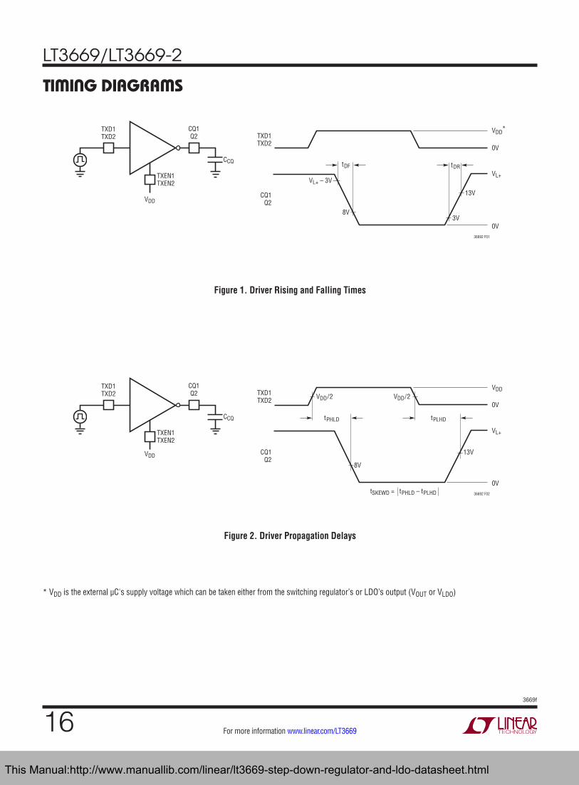
Figure 1. Driver Rising and Falling Times
Figure 2. Driver Propagation Delays
* VDD is the external µC's supply voltage which can be taken either from the switching regulator’s or LDO’s output (VOUT or VLDO)
VDD
8V
VL+ – 3V
0V
VL+
3V
0V
VDD
36692 F01
tDF tDR
CQ1Q2
TXD1TXD2
13V
CCQ
CQ1Q2
TXD1TXD2
TXEN1TXEN2
*
13V
8V
0V
VL+
0V
VDD
VDD
VDD/2VDD/2
tPLHD
36692 F02tSKEWD = tPHLD – tPLHD
tPHLD
CQ1Q2
TXD1TXD2
CCQ
CQ1Q2
TXD1TXD2
TXEN1TXEN2
This Manual:http://www.manuallib.com/linear/lt3669-step-down-regulator-and-ldo-datasheet.html
LT3669/LT3669-2
173669f
For more information www.linear.com/LT3669
TiMing DiagraMs
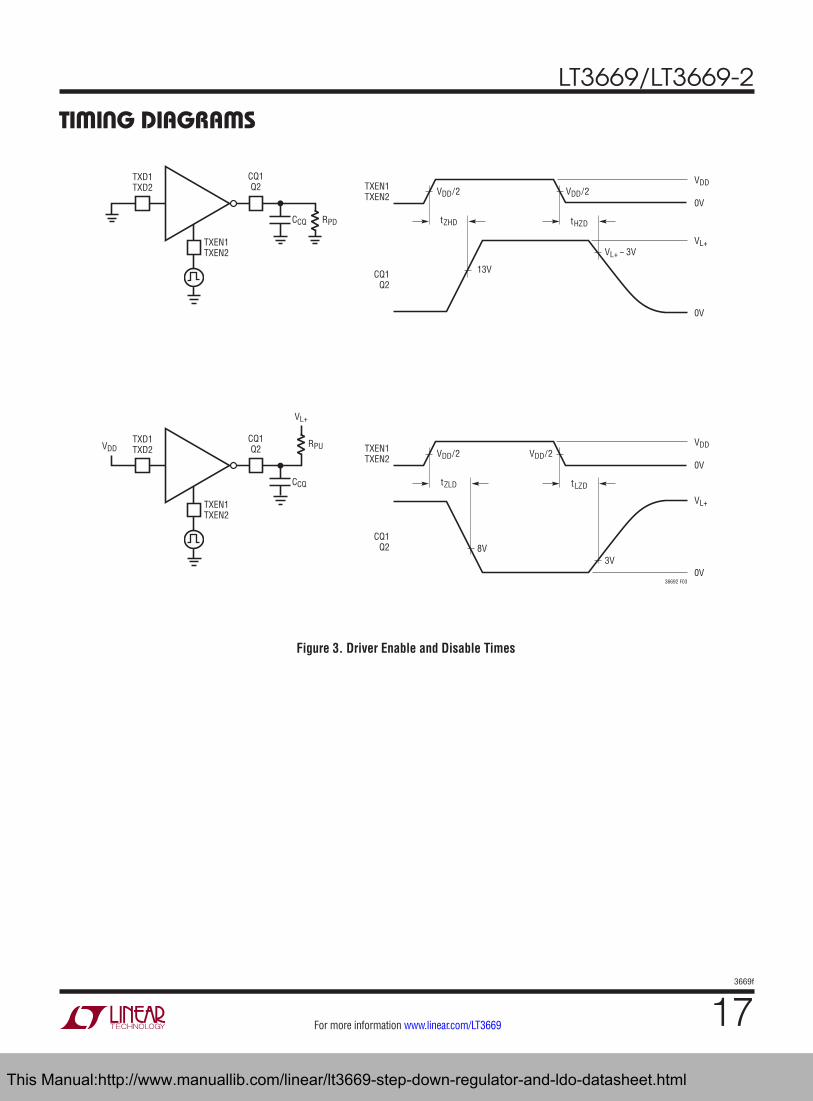
Figure 3. Driver Enable and Disable Times
36692 F03
VL+
0V
VDDVDD/2VDD/2
VDD
CCQ
RPU
tLZDtZLD
0V3V
VL+ – 3V
8V
13V
CQ1Q2
CQ1Q2
TXEN1TXEN2
TXD1TXD2
TXEN1TXEN2
VL+
0V
VL+
0V
VDDVDD/2VDD/2
tHZDtZHD
CQ1Q2
TXEN1TXEN2
CCQ RPD
CQ1Q2
TXD1TXD2
TXEN1TXEN2
This Manual:http://www.manuallib.com/linear/lt3669-step-down-regulator-and-ldo-datasheet.html
LT3669/LT3669-2
183669f
For more information www.linear.com/LT3669
TiMing DiagraMs
Figure 4. Receiver Propagation Delays
Figure 5. Receiver Detection and Noise Filter
Figure 6. Power-On Reset Waveforms
36692 F04
0V
VL+
0V
VDD
8V
13V
tPLHR
RXD1
CQ1
tPHLR
VDD
CQ1
RPURXD1
CQ1
tSKEWR = tPHLR – tPLHR
36692 F05
0V
0V
VL+
VDD
VTHHVTHL
< TBIT /16
TBIT
> TBIT /16SHORT GLITCH
REJECTEDLONG GLITCHDETECTED
RXD1
CQ1
TBIT
36692 F06
0V
VDD
VRSTTHVOUT
(VLDO)
VDD/2
tUV
RST
tRST
RPURST
PORCONTROL
VDD
This Manual:http://www.manuallib.com/linear/lt3669-step-down-regulator-and-ldo-datasheet.html
LT3669/LT3669-2
193669f
For more information www.linear.com/LT3669
TXEN1 TXD1
36692 F07
0V
0V
0V
VL+
VL+
VL+
VL+
0V
0mA
500mA
100mA
VDD
VDD
VDDVDD/2VDD/2
VDD/2
tWU*
tDWU
tDWU
TXD1
TXEN1
IPD
WAKE
CQ1
TXD1
TXEN1
WAKE
CQ1
VDD/2
tLZW
tHZD
VL+ – 3V
VL+ – VRQH
VRQL
RPU
RPD
IPD
WAKE
CQ1
TXEN1 TXD1
WAKE-UPDETECT
TXEN1 TXD1
RPU
RPU
IPUWAKE
CQ1
TXEN1 TXD1
WAKE-UPDETECT
0mA
500mA
100mA
tWU
IPU
VDD/2
0V
0V
0V
0V
VDD
VDD
VDDVDD/2
VDD/2
tLZW
tLZD
3V
VDD/2
VDD
VDD
TiMing DiagraMs
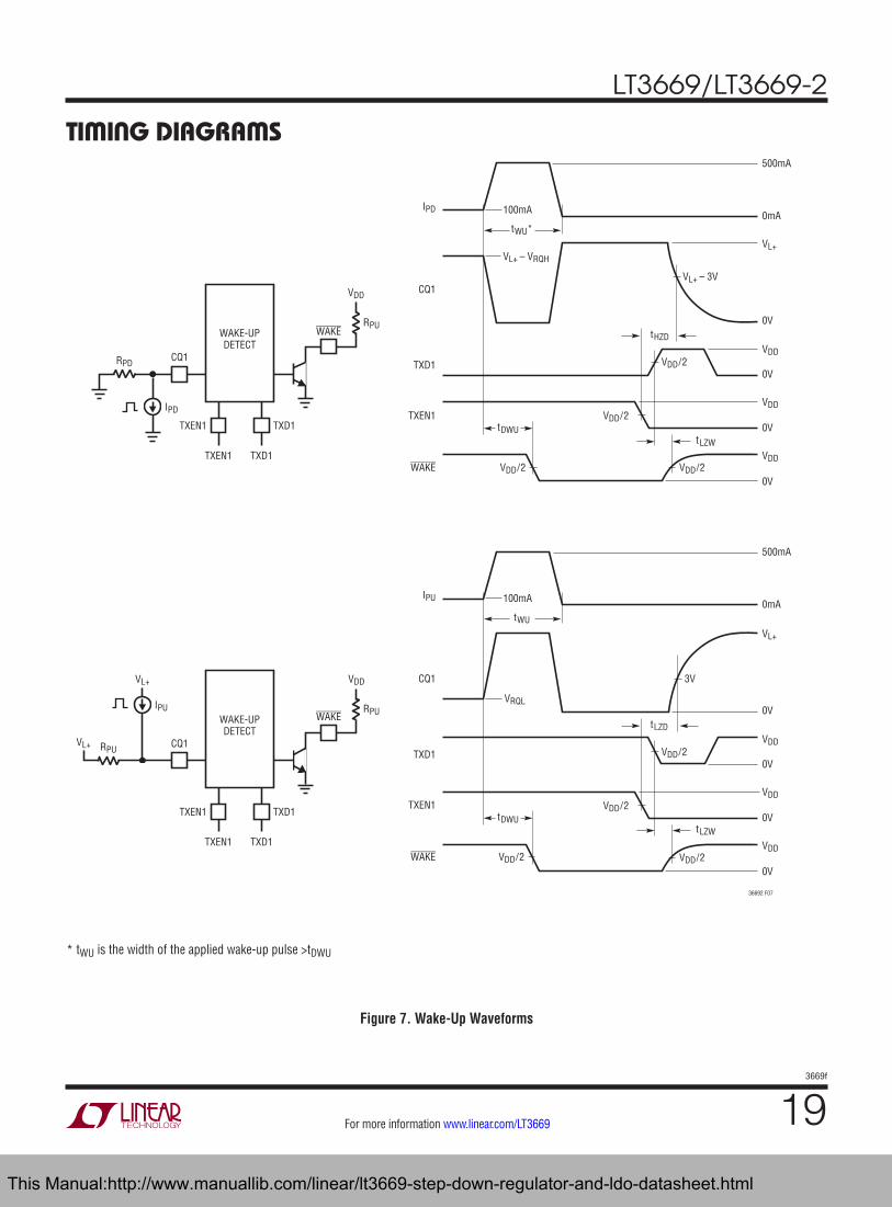
Figure 7. Wake-Up Waveforms
* tWU is the width of the applied wake-up pulse >tDWU
This Manual:http://www.manuallib.com/linear/lt3669-step-down-regulator-and-ldo-datasheet.html
LT3669/LT3669-2
203669f
For more information www.linear.com/LT3669
operaTionThe LT3669/LT3669-2 is a complete industrial slave in-terface, including a switching voltage regulator, an LDO, a data transceiver with wake-up detect, a second driver and a power-on reset circuit. This set of features allows a typical industrial slave device to be built with just a sensor or actuator, the LT3669 and a microcontroller to provide the digital conversion and signal processing.
The line transceiver circuitry includes a receiver that monitors the CQ1 line for data and sets the output RXD1 accordingly, and a driver that drives the CQ1 line controlled by inputs TXEN1 and TXD1. Additionally, a second driver controlled by inputs TXEN2 and TXD2 drives the Q2 line. Both drivers share a common user-adjustable sink/source current limit (up to ±330mA, typical) by connecting a resistor to AGND at the ILIM pin. The drivers feature four modes of operation: push-pull, pull-up only, pull-down only, as well as a high impedance mode.
The CQ1 driver also includes a built-in wake-up pulse detect circuitry that senses when the output CQ1 is forced oppo-site of its driven value for a minimum of 75µs. When this wake-up signal is detected, the WAKE output pulls low to alert the host system that a data transmission is expected. The WAKE output returns to high impedance again when the host acknowledges the wake-up request by executing the handshake sequence of setting the TXEN1 input low (receive mode) and toggling the TXD1 input, or under an internal reset event. Both drivers support COM1 (4.8kb/s), COM2 (38.4kb/s) and COM3 (230.4kb/s) communication modes. The receiver supports logic swings on the CQ1 pin in accordance with the IO-Link communication standard. Tying CQ1 and Q2 pins together, as well as pins TXD1 and TXD2 and TXEN1 and TXEN2, increases the overall current capability.
The drivers are equipped with a pulsing scheme that allows them to safely drive heavy capacitive loads and incandescent bulbs. Outputs SC1 and SC2 will flag if CQ1 or Q2 outputs are forced within 2.95V of the opposite rail they are trying to reach. A blanking time prevents false alarms during normal output transitions.
The switching regulator of the LT3669 integrates the catch diode and provides a typical conversion efficiency greater than 60% at its maximum load current of 100mA with a standard industrial supply voltage of 24V at the L+ pin and 5V output. The LT3669-2 requires an external catch diode and provides a typical efficiency greater than 75% at its maximum load current of 300mA. Compared to a linear regulator, this drastically minimizes power dissipation in the slave device, and minimizes current draw on the in-dustrial 24V line. The regulator features an on-chip power switch and built-in compensation, soft-start, current limit, and other support circuits required to maintain a robust, well regulated output voltage. The switching frequency is adjustable with a resistor to AGND at the RT pin to allow the circuit to be optimized either for space or efficiency, and the frequency can be synchronized to an external clock to minimize interference with signal processing circuits. A precision UVLO circuit allows the system to shut down at a user-selectable voltage.
An on-chip LDO linear regulator provides a second out-put voltage at up to 150mA. The LDO has current limit with foldback for robust performance in fault conditions.
The reset output (RST) goes low at start-up and remains low until each regulated output is within 7.3% of its final value and the user-adjustable reset timer has expired. This ensures that the supply voltages are in regulation and stable before the signal processing circuitry is allowed to start. The reset timer is programmed with an external capacitor to AGND at the CPOR pin.
The LT3669 tolerates transient swings to +60V from GND and –60V from L+ on the CQ1 and Q2 pins without damage.
Logic inputs TXD1, TXD2, TXEN1, TXEN2 and SR feature 900mV thresholds and logic input SYNC a 1.5V threshold to interface easily with low voltage logic. All logic outputs (RXD1, RST, SC1, SC2 and WAKE) are open collector.
This Manual:http://www.manuallib.com/linear/lt3669-step-down-regulator-and-ldo-datasheet.html
LT3669/LT3669-2
213669f
For more information www.linear.com/LT3669
LINE DRIVERS
Setting the Current Limit
The LT3669 line drivers have an accurate current limit that is programmed by a resistor tied from the ILIM pin to ground. Table 1 lists the necessary RILIM values for desired current limits. Tying the ILIM pin to ground sets the default current limit of 140mA.
Table 1. Current Limit vs RILIM ValueCURRENT LIMIT (mA) RILIM VALUE (kΩ)
70 221
90 169
130 113
170 84.5
210 68.1
250 56.2
290 48.7
330 42.2
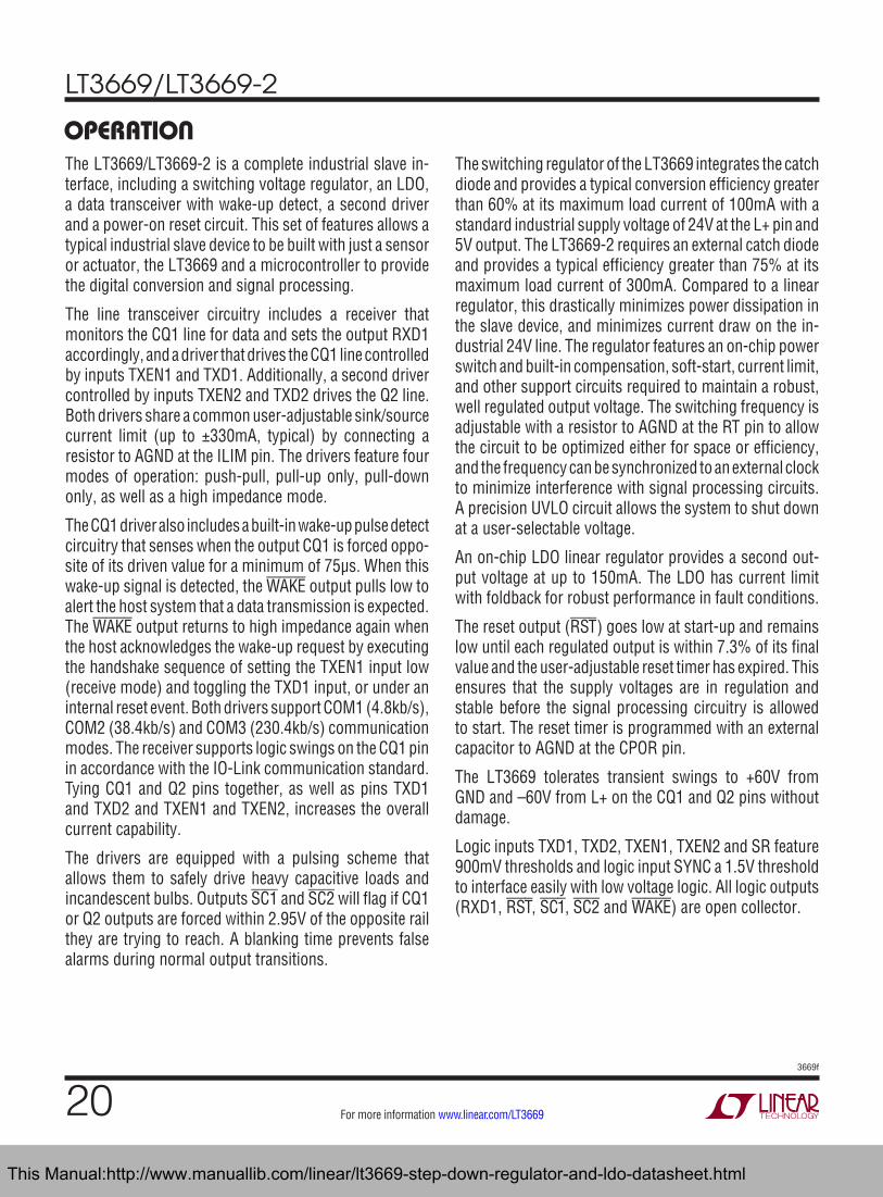
The accurate current-limit circuit loop has a time constant of approximately 10µs. Additionally, high speed current-limit clamps protect the part in case of heavy loads or short-circuits. Figure 8 depicts the high and low side driver’s output current waveforms in a short-circuit condition.
Slew Rate Control
The LT3669 line drivers feature a controlled programmable slew rate for optimum EMC performance. CQ1 and Q2 rising and falling times can be programmed using the SR
applicaTions inForMaTioninput pin and are independent of the L+ supply voltage. Forcing SR below 0.4V sets the rising/falling times to a typical value of 1.6µs/2.1µs. Forcing SR above 0.9V sets these times to a typical value of 260ns/340ns.
The LT3669 output drivers achieve a well controlled slew rate for a wide variety of output loads while of-fering a low residual voltage (< 2.1V) for output load currents of up to 250mA. In order to do so, the output drivers switch to a low residual voltage mode after a defined time once the TXD signal has toggled. This time is dependent on the SR pin input level. For SR low, the drivers will enter this mode after 8.5µs; for SR high, after 1.8µs. This gives enough time for the controlled slew rate mechanism to bring the outputs to within 2.95V from the supply rails, therefore minimizing EMI during the main part of the level transition. Once the timer is expired the outputs will further approach the supply rails to within 2.1V. Figure 9 depicts the output waveforms during transitions.
Driving Heavy Loads
The LT3669 is equipped with a pulsing mechanism to drive heavy output loads like big capacitors and incandescent bulbs, and also protect it against output short-circuit conditions.
Under heavy load or output short-circuit conditions, the power dissipated in the switches may increase its local junction temperature to excessive levels if the loads were driven continuously. In order to maintain robust operation, the LT3669 output drivers use pulses of variable on-time and fixed off-time (2.2ms typical) to cool the drivers down
Figure 8. Current Limit Waveform in Short-Circuit Figure 9. Output Waveforms During a Transition
100µs/DIV
VTXEN15V/DIV
0A
ICQ10.5A/DIV
0A
ICQ10.5A/DIV
36692 F08
RILIM = 42.2kΩVL+ = 24V
LOW SIDE(SHORTED TO L+)
HIGH SIDE(SHORTED TO GND)
2µs/DIV
0V
VCQ110V/DIV
0V
VCQ110V/DIV
36692 F09
RILIM = 42.2kΩVL+ = 24VSR = 0V
100Ω PULL-DOWN
100Ω PULL-UP
This Manual:http://www.manuallib.com/linear/lt3669-step-down-regulator-and-ldo-datasheet.html
LT3669/LT3669-2
223669f
For more information www.linear.com/LT3669
50ms/DIV
VCQ1/Q25V/DIV
VSC15V/DIV
VSC25V/DIV
36692 F10
12V/5W BULBVL+ = 12VRILIM = 42.2kΩ
5ms/DIV
VCQ11V/DIV
VSC15V/DIV
0V
36692 F11
RILIM = 42.2kΩ
2ms/DIV
VTXEN15V/DIV
VCQ10.5V/DIV
VSC15V/DIV
36692 F12
RILIM = 42.2kΩ
applicaTions inForMaTionuntil the residual voltages approach within 2.95V of the intended power rail, in which case the loads are driven continuously. The on-time depends on the sum of the residual voltages for the active switches (provided that the residual voltage is higher than 2.95V) and since their current limit is fixed, it is inversely proportional to their power dissipation. The lower the power dissipated by the switches, the longer the on-time, thus optimizing the time to drive these heavy loads fully. In order to account for the case of normal load slew rate, the internal on-time timer only increases after a blanking period dependent on the SR setting. A thermal shutdown circuit with a trigger tem-perature of 140°C (typical) provides additional protection.
Short-Circuit and Thermal Shutdown Flags SC1 and SC2
A short-circuit is defined as the condition where the driver’s output is within 2.95V from the opposite targeted rail, for instance if the CQ1 output is programmed to be high level (close to VL+) but stays within 2.95V from GND. If either CQ1 or Q2 is short-circuited, the internal pulsing mechanism and thermal shutdown circuitry will protect the drivers. Open-collector outputs SC1 and SC2 will pull low during short-circuit events on CQ1 an Q2, respectively.
A heavy output load can be interpreted as a short-circuit condition during the first pulses, and SC1 and SC2 outputs will flag it accordingly. This information can be used by an external microcontroller to decide whether there is a real short-circuit or a heavy load is attached to the outputs. A heavy load requires a minimum amount of time to bring the driver’s output outside of the short-circuit range. By setting timers using SC1 and SC2, a short-circuit condition can be found and the microcontroller will react accordingly (by disabling the affected driver, for example).
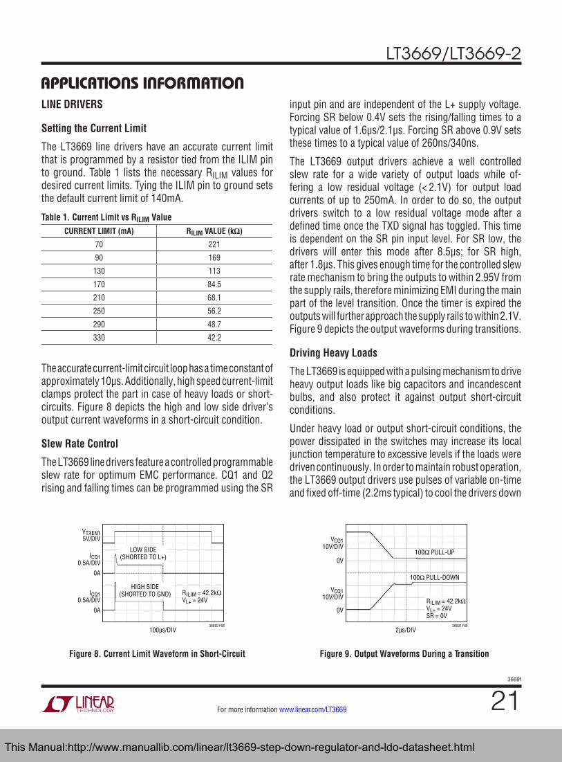
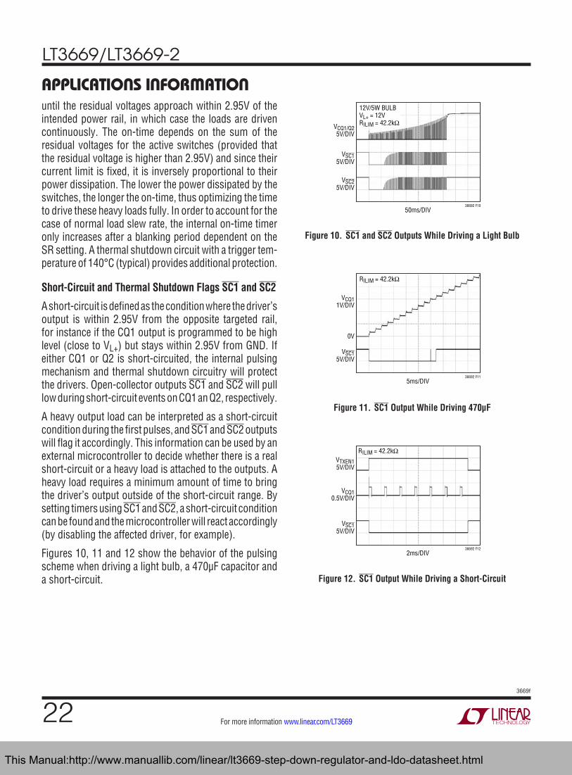
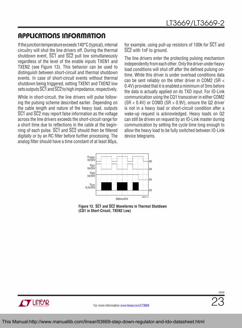
Figures 10, 11 and 12 show the behavior of the pulsing scheme when driving a light bulb, a 470µF capacitor and a short-circuit.
Figure 10. SC1 and SC2 Outputs While Driving a Light Bulb
Figure 11. SC1 Output While Driving 470µF
Figure 12. SC1 Output While Driving a Short-Circuit
This Manual:http://www.manuallib.com/linear/lt3669-step-down-regulator-and-ldo-datasheet.html
LT3669/LT3669-2
233669f
For more information www.linear.com/LT3669
applicaTions inForMaTion
Figure 13. SC1 and SC2 Waveforms in Thermal Shutdown (CQ1 in Short-Circuit, TXEN2 Low)
If the junction temperature exceeds 140°C (typical), internal circuitry will shut the line drivers off. During the thermal shutdown event, SC1 and SC2 pull low simultaneously regardless of the level of the enable inputs TXEN1 and TXEN2 (see Figure 13). This behavior can be used to distinguish between short-circuit and thermal shutdown events. In case of short-circuit events without thermal shutdown being triggered, setting TXEN1 and TXEN2 low sets outputs SC1 and SC2 to high impedance, respectively.
While in short-circuit, the line drivers will pulse follow-ing the pulsing scheme described earlier. Depending on the cable length and nature of the heavy load, outputs SC1 and SC2 may report false information as the voltage across the line drivers exceeds the short-circuit range for a short time due to reflections in the cable at the begin-ning of each pulse. SC1 and SC2 should then be filtered digitally or by an RC filter before further processing. The analog filter should have a time constant of at least 80µs,
for example, using pull-up resistors of 100k for SC1 and SC2 with 1nF to ground.
The line drivers enter the protecting pulsing mechanism independently from each other. Only the driver under heavy load conditions will shut off after the defined pulsing on-time. While this driver is under overload conditions data can be sent reliably on the other driver in COM2 (SR < 0.4V) provided that it is enabled a minimum of 3ms before the data is actually applied on its TXD input. For IO-Link communication using the CQ1 transceiver in either COM2 (SR < 0.4V) or COM3 (SR > 0.9V), ensure the Q2 driver is not in a heavy load or short-circuit condition after a wake-up request is acknowledged. Heavy loads on Q2 can still be driven on request by an IO-Link master during communication by setting the cycle time long enough to allow the heavy load to be fully switched between IO-Link device telegrams.
500ms/DIV
VTXEN15V/DIV 0V
0V
0V
0V
VCQ10.2V/DIV
VSC15V/DIV
VSC25V/DIV
36692 F13
This Manual:http://www.manuallib.com/linear/lt3669-step-down-regulator-and-ldo-datasheet.html
LT3669/LT3669-2
243669f
For more information www.linear.com/LT3669
applicaTions inForMaTionReceiver
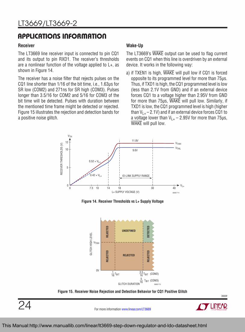
The LT3669 line receiver input is connected to pin CQ1 and its output to pin RXD1. The receiver’s thresholds are a nonlinear function of the voltage applied to L+, as shown in Figure 14.
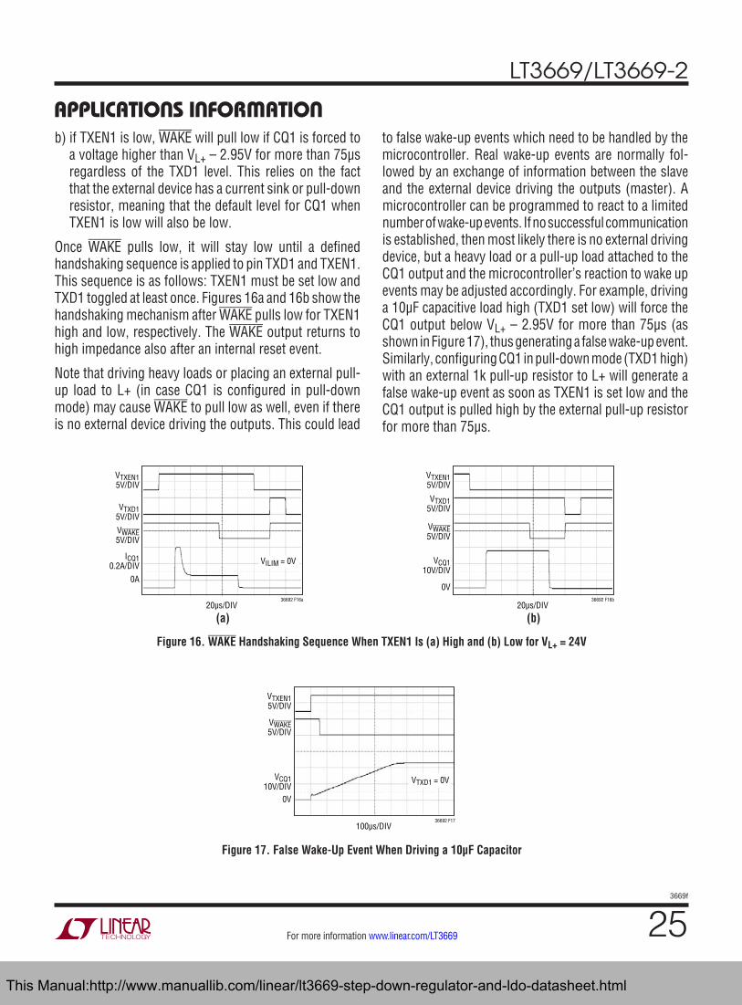
The receiver has a noise filter that rejects pulses on the CQ1 line shorter than 1/16 of the bit time, i.e., 1.63μs for SR low (COM2) and 271ns for SR high (COM3). Pulses longer than 3.5/16 for COM2 and 5/16 for COM3 of the bit time will be detected. Pulses with duration between the mentioned time frame might be detected or rejected. Figure 15 illustrates the rejection and detection bands for a positive noise glitch.
Figure 14. Receiver Thresholds vs L+ Supply Voltage
Figure 15. Receiver Noise Rejection and Detection Behavior for CQ1 Positive Glitch
Wake-Up
The LT3669’s WAKE output can be used to flag current events on CQ1 when this line is overdriven by an external device. It works in the following way:
a) if TXEN1 is high, WAKE will pull low if CQ1 is forced opposite to its programmed level for more than 75µs. Thus, if TXD1 is high, the CQ1 programmed level is low (less than 2.1V from GND) and if an external device forces CQ1 to a voltage higher than 2.95V from GND for more than 75µs, WAKE will pull low. Similarly, if TXD1 is low, the CQ1 programmed level is high (higher than VL+ – 2.1V) and if an external device forces CQ1 to a voltage lower than VL+ – 2.95V for more than 75µs, WAKE will pull low.
L+ SUPPLY VOLTAGE (V)0
0
RECE
IVER
THR
ESHO
LDS
(V) 12
14 18 30
11.8V
9.6V
IO-LINK SUPPLY RANGE
36692 F14
0.42 × VL+
VL+
0.52 × VL+
VTHH
VTH
VTHL10
5
7.5 10 40
GLITCH DURATION
0V
GLIT
CH H
IGH
LEVE
L
UNDEFINED
REJECTED
REJE
CTED
REJE
CTED
DETE
CTED
REJE
CTED
36692 F15
VTHH
TBIT3.516
TBIT516
(COM2)
(COM3)
TBIT116
This Manual:http://www.manuallib.com/linear/lt3669-step-down-regulator-and-ldo-datasheet.html
LT3669/LT3669-2
253669f
For more information www.linear.com/LT3669
applicaTions inForMaTionb) if TXEN1 is low, WAKE will pull low if CQ1 is forced to
a voltage higher than VL+ – 2.95V for more than 75µs regardless of the TXD1 level. This relies on the fact that the external device has a current sink or pull-down resistor, meaning that the default level for CQ1 when TXEN1 is low will also be low.
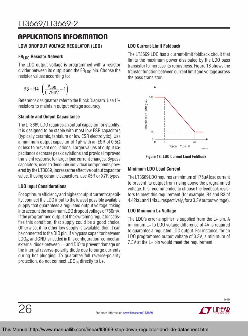
Once WAKE pulls low, it will stay low until a defined handshaking sequence is applied to pin TXD1 and TXEN1. This sequence is as follows: TXEN1 must be set low and TXD1 toggled at least once. Figures 16a and 16b show the handshaking mechanism after WAKE pulls low for TXEN1 high and low, respectively. The WAKE output returns to high impedance also after an internal reset event.
Note that driving heavy loads or placing an external pull-up load to L+ (in case CQ1 is configured in pull-down mode) may cause WAKE to pull low as well, even if there is no external device driving the outputs. This could lead
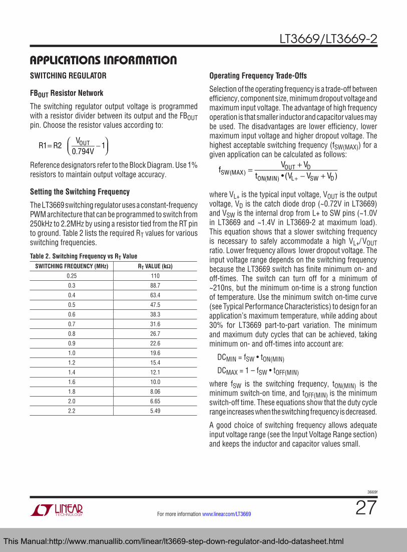
to false wake-up events which need to be handled by the microcontroller. Real wake-up events are normally fol-lowed by an exchange of information between the slave and the external device driving the outputs (master). A microcontroller can be programmed to react to a limited number of wake-up events. If no successful communication is established, then most likely there is no external driving device, but a heavy load or a pull-up load attached to the CQ1 output and the microcontroller’s reaction to wake up events may be adjusted accordingly. For example, driving a 10µF capacitive load high (TXD1 set low) will force the CQ1 output below VL+ – 2.95V for more than 75µs (as shown in Figure 17), thus generating a false wake-up event. Similarly, configuring CQ1 in pull-down mode (TXD1 high)with an external 1k pull-up resistor to L+ will generate a false wake-up event as soon as TXEN1 is set low and the CQ1 output is pulled high by the external pull-up resistor for more than 75µs.
Figure 16. WAKE Handshaking Sequence When TXEN1 Is (a) High and (b) Low for VL+ = 24V
Figure 17. False Wake-Up Event When Driving a 10µF Capacitor
20µs/DIV
VTXEN15V/DIV
VWAKE5V/DIV
VTXD15V/DIV
0A
ICQ10.2A/DIV
36692 F16a
VILIM = 0V
20µs/DIV
VTXEN15V/DIV
VWAKE5V/DIV
VTXD15V/DIV
0V
VCQ110V/DIV
36692 F16b
100µs/DIV
VTXEN15V/DIV
VWAKE5V/DIV
0V
VCQ110V/DIV
36692 F17
VTXD1 = 0V
(a) (b)
This Manual:http://www.manuallib.com/linear/lt3669-step-down-regulator-and-ldo-datasheet.html
LT3669/LT3669-2
263669f
For more information www.linear.com/LT3669
applicaTions inForMaTionLOW DROPOUT VOLTAGE REGULATOR (LDO)
FBLDO Resistor Network
The LDO output voltage is programmed with a resistor divider between its output and the FBLDO pin. Choose the resistor values according to:
R3 = R4
VLDO0.794V
− 1
Reference designators refer to the Block Diagram. Use 1% resistors to maintain output voltage accuracy.
Stability and Output Capacitance
The LT3669 LDO requires an output capacitor for stability. It is designed to be stable with most low ESR capacitors (typically ceramic, tantalum or low ESR electrolytic). Use a minimum output capacitor of 1μF with an ESR of 0.5Ω or less to prevent oscillations. Larger values of output ca-pacitance decrease peak deviations and provide improved transient response for larger load current changes. Bypass capacitors, used to decouple individual components pow-ered by the LT3669, increase the effective output capacitor value. If using ceramic capacitors, use X5R or X7R types.
LDO Input Considerations
For optimum efficiency and highest output current capabil-ity, connect the LDO input to the lowest possible available supply that guarantees a regulated output voltage, taking into account the maximum LDO dropout voltage of 750mV. If the programmed output of the switching regulator satis-fies this condition, that supply could be a good choice. Otherwise, if no other low supply is available, then it can be connected to the DIO pin. If a bypass capacitor between LDOIN and GND is needed in this configuration, connect an external diode between L+ and DIO to prevent damage on the internal reverse-polarity diode due to surge currents during hot plugging. To guarantee full reverse-polarity protection, do not connect LDOIN directly to L+.
LDO Current-Limit Foldback
The LT3669 LDO has a current-limit foldback circuit that limits the maximum power dissipated by the LDO pass transistor to increase its robustness. Figure 18 shows the transfer function between current limit and voltage across the pass transistor.
Figure 18. LDO Current Limit Foldback
VLDOIN – VLDO (V)0
0
LDO
CURR
ENT
LIM
IT (m
A)
35
180
6 35
36692 F18
Minimum LDO Load Current
The LT3669 LDO requires a minimum of 175µA load current to prevent its output from rising above the programmed voltage. It is recommended to choose the feedback resis-tors to meet this requirement (for example, R4 and R3 of 4.42kΩ and 14kΩ, respectively, for a 3.3V output voltage).
LDO Minimum L+ Voltage
The LDO’s error amplifier is supplied from the L+ pin. A minimum L+ to LDO voltage difference of 4V is required to guarantee a regulated LDO output. For instance, for an LDO programmed output voltage of 3.3V, a minimum of 7.3V at the L+ pin would meet the requirement.
This Manual:http://www.manuallib.com/linear/lt3669-step-down-regulator-and-ldo-datasheet.html
LT3669/LT3669-2
273669f
For more information www.linear.com/LT3669
applicaTions inForMaTionSWITCHING REGULATOR
FBOUT Resistor Network
The switching regulator output voltage is programmed with a resistor divider between its output and the FBOUT pin. Choose the resistor values according to:
R1= R2
VOUT0.794V
− 1
Reference designators refer to the Block Diagram. Use 1% resistors to maintain output voltage accuracy.
Setting the Switching Frequency
The LT3669 switching regulator uses a constant-frequency PWM architecture that can be programmed to switch from 250kHz to 2.2MHz by using a resistor tied from the RT pin to ground. Table 2 lists the required RT values for various switching frequencies.
Table 2. Switching Frequency vs RT ValueSWITCHING FREQUENCY (MHz) RT VALUE (kΩ)
0.25 110
0.3 88.7
0.4 63.4
0.5 47.5
0.6 38.3
0.7 31.6
0.8 26.7
0.9 22.6
1.0 19.6
1.2 15.4
1.4 12.1
1.6 10.0
1.8 8.06
2.0 6.65
2.2 5.49
Operating Frequency Trade-Offs
Selection of the operating frequency is a trade-off between efficiency, component size, minimum dropout voltage and maximum input voltage. The advantage of high frequency operation is that smaller inductor and capacitor values may be used. The disadvantages are lower efficiency, lower maximum input voltage and higher dropout voltage. The highest acceptable switching frequency (fSW(MAX)) for a given application can be calculated as follows:
fSW(MAX) =
VOUT + VDtON(MIN) • (VL+ − VSW + VD)
where VL+ is the typical input voltage, VOUT is the output voltage, VD is the catch diode drop (~0.72V in LT3669) and VSW is the internal drop from L+ to SW pins (~1.0V in LT3669 and ~1.4V in LT3669-2 at maximum load). This equation shows that a slower switching frequency is necessary to safely accommodate a high VL+/ VOUT ratio. Lower frequency allows lower dropout voltage. The input voltage range depends on the switching frequency because the LT3669 switch has finite minimum on- and off-times. The switch can turn off for a minimum of ~210ns, but the minimum on-time is a strong function of temperature. Use the minimum switch on-time curve (see Typical Performance Characteristics) to design for an application’s maximum temperature, while adding about 30% for LT3669 part-to-part variation. The minimum and maximum duty cycles that can be achieved, taking minimum on- and off-times into account are:
DCMIN = fSW • tON(MIN)
DCMAX = 1 – fSW • tOFF(MIN)
where fSW is the switching frequency, tON(MIN) is the minimum switch-on time, and tOFF(MIN) is the minimum switch-off time. These equations show that the duty cycle range increases when the switching frequency is decreased.
A good choice of switching frequency allows adequate input voltage range (see the Input Voltage Range section) and keeps the inductor and capacitor values small.
This Manual:http://www.manuallib.com/linear/lt3669-step-down-regulator-and-ldo-datasheet.html
LT3669/LT3669-2
283669f
For more information www.linear.com/LT3669
applicaTions inForMaTionInput Voltage Range
The minimum input voltage is determined by either the LT3669’s minimum operating voltage of 7.5V or by its maximum duty cycle (see equation in the Operating Fre-quency Trade-Offs section). The minimum input voltage due to duty cycle is:
VL+(MIN) =
VOUT + VD1− fSW • tOFF(MIN)
− VD + VSW
where VL+(MIN) is the minimum input voltage, and tOFF(MIN) is the minimum switch-off time. Note that higher switch-ing frequency will increase the minimum input voltage. If a lower dropout voltage is desired, a lower switching frequency should be used.
The maximum input voltage for LT3669 applications depends on switching frequency, the absolute maximum ratings of the L+ and BST pins, and the operating mode. The LT3669 can operate continuously from input voltages up to 40V. Input voltage transients of up to 60V are also safely withstood. However, note that if VL+ exceeds VOVLO (43V typical), the LT3669 will stop switching, allowing the output to fall out of regulation.
For a given application in which the switching frequency and the output voltage are already fixed, the maximum input voltage that guarantees optimum output voltage ripple for that application can be found by applying the following expression:
VL+(MAX) =
VOUT + VDfSW • tON(MIN)
− VD + VSW
where VL+(MAX) is the maximum operating input voltage, VOUT is the output voltage, VD is the catch diode drop (~0.72V in LT3669) and VSW is the internal drop from L+ to SW pins (~1.0V in LT3669 and ~1.4V in LT3669-2 at maximum load), fSW is the switching frequency (set by RT), and tON(MIN) is the minimum switch-on time. Note that a higher switching frequency will reduce the maximum operating input voltage. Conversely, a lower switching frequency is necessary to achieve optimum operation at high input voltages.
Special attention must be paid when the output is in start-up, short-circuit, or other overload conditions.
In these cases, the LT3669 tries to bring the output in regulation by driving lots of current into the output load. During these events, the inductor peak current might easily reach and even exceed the maximum current limit of the LT3669, especially in those cases where the switch already operates at minimum on-time. The circuitry monitoring the current through the catch diode prevents the switch from turning on again if the inductor valley current is above 0.2A and 0.45A nominal values for LT3669 and LT3669-2, respectively. In these cases, the inductor peak current is therefore the maximum current limit of the LT3669 plus the additional current overshoot during the turn-off delay due to minimum on-time:
IL(PEAK) = ISW(LIM) +
VL+(MAX) − VOUTOL
L• tON(MIN)
where IL(PEAK) is the peak inductor current, ISW(LIM) is the switch current limit (0.325A in LT3669 and 0.65A in LT3669-2), VL+(MAX) is the maximum expected input voltage, L is the inductor value, tON(MIN) is the minimum on-time and VOUTOL is the output voltage under the overload condition. The part is robust enough to survive prolonged operation under these conditions as long as the peak in-ductor current does not exceed 0.6A in LT3669 and 1.3A in LT3669-2. Inductor current saturation and excessive junction temperature may further limit performance.
Inductor Selection and Maximum Output Current
A good first choice for the inductor value is:
L = (VOUT + VD) •k
fSW
(k = 9 in LT3669, k = 3.6 in LT3669-2)
where fSW is the switching frequency in MHz, VOUT is the output voltage, VD is the catch diode drop (~0.72V in LT3669) and L is the inductor value in μH.
The inductor’s RMS current rating must be greater than the maximum load current and its saturation current should be about 30% higher. To keep the efficiency high, the series resistance (DCR) should be less than 0.1Ω, and the core material should be intended for high frequency applications. Table 3 lists several vendors of inductors.
This Manual:http://www.manuallib.com/linear/lt3669-step-down-regulator-and-ldo-datasheet.html
LT3669/LT3669-2
293669f
For more information www.linear.com/LT3669
applicaTions inForMaTionTable 3. Inductor Vendors
VENDOR URL
Murata www.murata.com
TDK www.componenttdk.com
Toko www.toko.com
Coilcraft www.coilcraft.com
Sumida www.sumida.com
Würth Elektronik www.we-online.com
Coiltronics www.cooperet.com
For robust operation in fault conditions (start-up or short-circuit) and high input voltage (>30V), choose the saturation current high enough to ensure that the inductor peak current does not exceed 0.6A and 1.3A for LT3669 and LT3669-2, respectively. For example, an LT3669-2 application running from an input voltage of 36V using a 33μH inductor with a saturation current of 0.8A will toler-ate the mentioned fault conditions.
The optimum inductor for a given application may differ from the one indicated by this simple design guide. A larger value inductor provides a higher maximum load cur-rent and reduces the output voltage ripple. If your load is lower than the maximum load current, then you can relax the value of the inductor and operate with higher ripple current. This allows the use of a physically smaller induc-tor, or one with a lower DCR resulting in higher efficiency. Be aware that if the inductance differs from the simple rule, then the maximum load current will depend on input voltage. In addition, low inductance may result in discon-tinuous mode operation, which further reduces maximum load current. For details of maximum output current and discontinuous mode operation, see Linear Technology’s Application Note 44. Finally, for duty cycles greater than 50% (VOUT/ VL+ > 0.5), a minimum inductance is required to avoid subharmonic oscillations:
LMIN = (VOUT + VD) •k
fSW
(k = 6.5 in LT3669; k = 2.6 in LT3669-2)
The current in the inductor is a triangle wave with an av-erage value equal to the load current. The peak inductor and switch current is:
ISW(PEAK) = IL(PEAK) = IOUT(MAX) +
Δ�IL
2
where IL(PEAK) is the peak inductor current, IOUT(MAX) is the maximum output load current, and ΔIL is the induc-tor ripple current. The LT3669 limits its switch current in order to protect itself and the system from overload faults. Therefore, the maximum output current that the LT3669 will deliver depends on the switch current limit, the induc-tor value and the input and output voltages.
When the switch is off, the voltage across the inductor is the output voltage plus the catch diode drop. This gives the peak-to-peak ripple current in the inductor:
ΔIL =
1− DC( ) • (VOUT + VD)L • fSW
where fSW is the switching frequency of the LT3669, DC is the duty cycle and L is the value of the inductor.
To maintain output regulation, the inductor peak current must be less than the switch current limit ILIM which is 0.325A (LT3669) and 0.65A (LT3669-2) at low duty cycles and decreases to 0.24A (LT3669) and 0.48A (LT3669-2). The maximum output current is also a function of the chosen inductor value and can be approximated by the following expression:
IOUT(MAX) = ILIM − ΔIL2
=
ILIM(DC = 0) • (1− 0.26 •DC) − ΔIL2
(ILIM(DC = 0) = 0.325A in LT3669;
ILIM(DC = 0) = 0.65A in LT3669-2)
Choosing an inductor value so that the ripple current is small will allow a maximum output current near the switch current limit.
One approach to choosing the inductor is to start with the simple rule—look at the available inductors, and choose one to meet cost or space goals. Then use these equations
This Manual:http://www.manuallib.com/linear/lt3669-step-down-regulator-and-ldo-datasheet.html
LT3669/LT3669-2
303669f
For more information www.linear.com/LT3669
applicaTions inForMaTionto check that the LT3669 will be able to deliver the required output current. Note again that these equations assume that the inductor current is continuous. Discontinuous operation occurs when IOUT is less than ΔIL/2.
Input Capacitor
Bypass the input of the LT3669 circuit with a ceramic ca-pacitor of X7R or X5R type. Do not use Y5V types, which have poor performance over temperature and applied voltage. A 4.7μF ceramic capacitor is adequate to bypass the LT3669 and will easily handle the ripple current. Note that larger input capacitance is required when a lower switching frequency is used. If the input power source has high impedance, or there is significant inductance due to long wires or cables, additional bulk capacitance may be necessary. This can be provided with a lower performance electrolytic capacitor.
Step-down regulators draw current from the input sup-ply in pulses with very fast rise and fall times. The input capacitor is required to reduce the resulting voltage ripple at the LT3669 and to force this very high frequency switching current into a tight local loop, minimizing EMI. A 4.7μF capacitor is capable of this task, but only if it is placed close to the LT3669 (see the PCB Layout section for more information). A second precaution regarding the ceramic input capacitor concerns the maximum input voltage rating of the LT3669. A ceramic input capacitor combined with trace or cable inductance forms a high-Q (underdamped) tank circuit. If the LT3669 circuit is plugged into a live supply, the input voltage can ring to twice its nominal value, possibly exceeding the LT3669’s voltage rating. For guidance see Application Note 88.
Output Capacitor and Output Ripple
The output capacitor has two essential functions. Along with the inductor, it filters the square wave generated by the LT3669 to produce the DC output. In this role, it de-termines the output ripple. Additionally, low impedance at the switching frequency is important. The second function is to store energy needed to satisfy transient loads and stabilize the LT3669’s control loop. Ceramic capacitors have very low equivalent series resistance (ESR) and
provide the best ripple performance. A good starting value is:
COUT = kVOUT • fSW
(k = 17 in LT3669; k = 43 in LT3669-2)
where fSW is in MHz, and COUT is the recommended output capacitance in μF. Use X5R or X7R types. This choice will provide low output ripple and good transient response. Transient performance can be improved with a higher value capacitor if combined with a phase lead capacitor (typically 22pF) between the output and the feedback pin (FBOUT). A lower value of output capacitor can be used to save space and cost but transient performance will suffer.
When choosing a capacitor, look carefully through the data sheet to find out what the actual capacitance is under operating conditions (applied voltage and temperature). A physically larger capacitor, or one with a higher voltage rating, may be required. High performance tantalum or electrolytic capacitors can be used for the output capaci-tor. Low ESR is important, so choose one that is intended for use in switching regulators. The ESR should be 0.05Ω or less. Such a capacitor will be larger than a ceramic capacitor and will have a larger capacitance, because the capacitor must be large to achieve low ESR.
LT3669-2 Diode Selection
The catch diode (D1 from the LT3669-2 Block Diagram) conducts current only during the switch-off time. Average forward current in normal operation is
ID(AVG) = IOUT • (1−DC)
where DC is the duty cycle. However, a diode with 1A cur-rent rating is required for overload conditions. For inputs up to the maximum operating voltage of 40V, use a diode with a reverse-voltage rating greater than the input voltage. If transients at the input of up to 60V are expected, use a diode with a reverse-voltage rating only higher than the maximum OVLO of 45V. If operating at high ambient tem-peratures, consider using a Schottky with low reverse leak-age. For example, Diodes, Inc. SBR1U40LP or DFLS160, ON Semiconductor MBRM140, and Central Semiconductor CMMSH1-60 are good choices for the catch diode.
This Manual:http://www.manuallib.com/linear/lt3669-step-down-regulator-and-ldo-datasheet.html
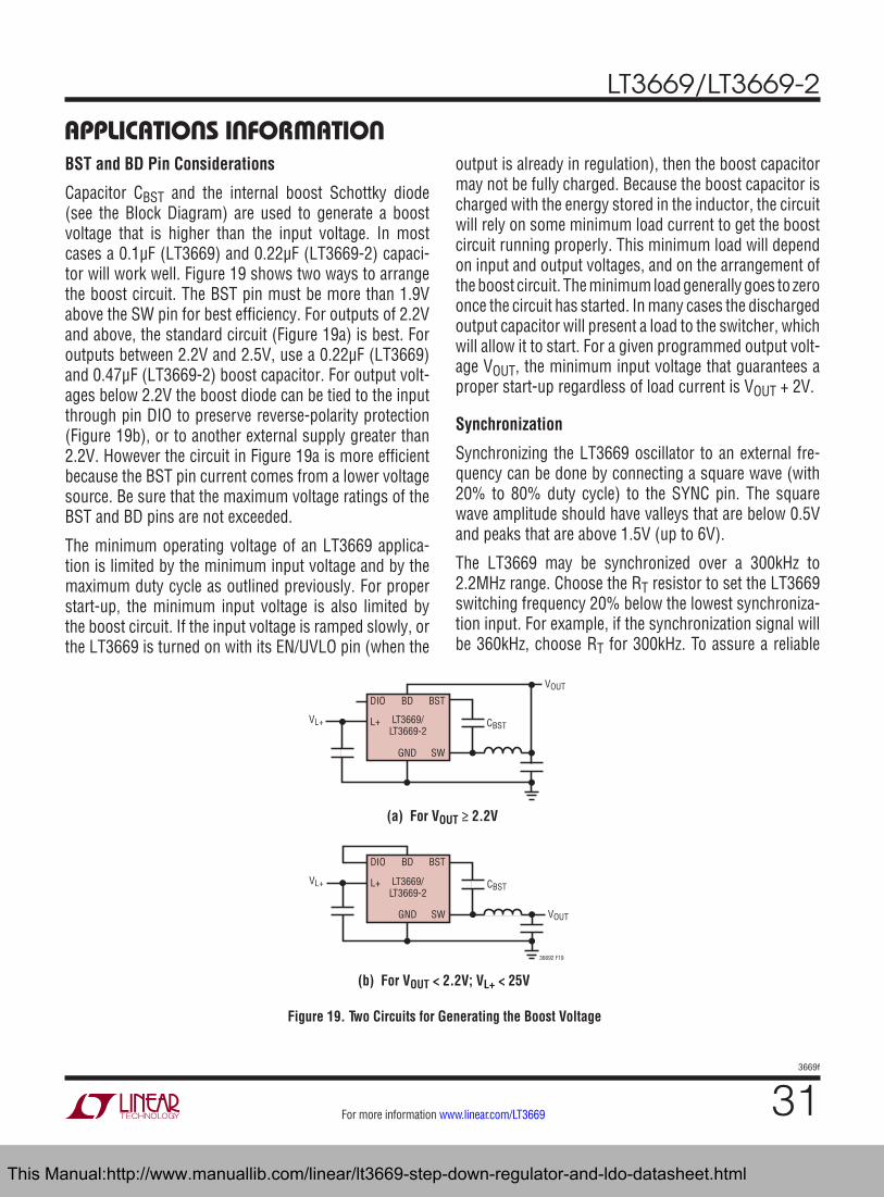
LT3669/LT3669-2
313669f
For more information www.linear.com/LT3669
applicaTions inForMaTionBST and BD Pin Considerations
Capacitor CBST and the internal boost Schottky diode (see the Block Diagram) are used to generate a boost voltage that is higher than the input voltage. In most cases a 0.1µF (LT3669) and 0.22µF (LT3669-2) capaci-tor will work well. Figure 19 shows two ways to arrange the boost circuit. The BST pin must be more than 1.9V above the SW pin for best efficiency. For outputs of 2.2V and above, the standard circuit (Figure 19a) is best. For outputs between 2.2V and 2.5V, use a 0.22µF (LT3669) and 0.47μF (LT3669-2) boost capacitor. For output volt-ages below 2.2V the boost diode can be tied to the input through pin DIO to preserve reverse-polarity protection (Figure 19b), or to another external supply greater than 2.2V. However the circuit in Figure 19a is more efficient because the BST pin current comes from a lower voltage source. Be sure that the maximum voltage ratings of the BST and BD pins are not exceeded.
The minimum operating voltage of an LT3669 applica-tion is limited by the minimum input voltage and by the maximum duty cycle as outlined previously. For proper start-up, the minimum input voltage is also limited by the boost circuit. If the input voltage is ramped slowly, or the LT3669 is turned on with its EN/UVLO pin (when the
output is already in regulation), then the boost capacitor may not be fully charged. Because the boost capacitor is charged with the energy stored in the inductor, the circuit will rely on some minimum load current to get the boost circuit running properly. This minimum load will depend on input and output voltages, and on the arrangement of the boost circuit. The minimum load generally goes to zero once the circuit has started. In many cases the discharged output capacitor will present a load to the switcher, which will allow it to start. For a given programmed output volt-age VOUT, the minimum input voltage that guarantees a proper start-up regardless of load current is VOUT + 2V.
Synchronization
Synchronizing the LT3669 oscillator to an external fre-quency can be done by connecting a square wave (with 20% to 80% duty cycle) to the SYNC pin. The square wave amplitude should have valleys that are below 0.5V and peaks that are above 1.5V (up to 6V).
The LT3669 may be synchronized over a 300kHz to 2.2MHz range. Choose the RT resistor to set the LT3669 switching frequency 20% below the lowest synchroniza-tion input. For example, if the synchronization signal will be 360kHz, choose RT for 300kHz. To assure a reliable
DIO BST
SW
LT3669/LT3669-2
BD
GND
VOUT
CBST
DIO
36692 F19
BST
SW
BD
GND
L+VL+
L+VL+
VOUT
CBSTLT3669/LT3669-2
Figure 19. Two Circuits for Generating the Boost Voltage
(a) For VOUT ≥ 2.2V
(b) For VOUT < 2.2V; VL+ < 25V
This Manual:http://www.manuallib.com/linear/lt3669-step-down-regulator-and-ldo-datasheet.html
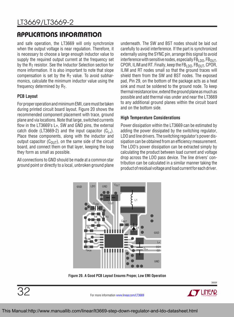
LT3669/LT3669-2
323669f
For more information www.linear.com/LT3669
applicaTions inForMaTionand safe operation, the LT3669 will only synchronize when the output voltage is near regulation. Therefore, it is necessary to choose a large enough inductor value to supply the required output current at the frequency set by the RT resistor. See the Inductor Selection section for more information. It is also important to note that slope compensation is set by the RT value. To avoid subhar-monics, calculate the minimum inductor value using the frequency determined by RT.
PCB Layout
For proper operation and minimum EMI, care must be taken during printed circuit board layout. Figure 20 shows the recommended component placement with trace, ground plane and via locations. Note that large, switched currents flow in the LT3669’s L+, SW and GND pins, the external catch diode (LT3669-2) and the input capacitor (CL+). Place these components, along with the inductor and output capacitor (COUT), on the same side of the circuit board, and connect them on that layer, keeping the loop they form as small as possible.
All connections to GND should be made at a common star ground point or directly to a local, unbroken ground plane
underneath. The SW and BST nodes should be laid out carefully to avoid interference. If the part is synchronized externally using the SYNC pin, arrange this signal to avoid interference with sensitive nodes, especially FBLDO, FBOUT, CPOR, ILIM and RT. Finally, keep the FBLDO, FBOUT, CPOR, ILIM and RT nodes small so that the ground traces will shield them from the SW and BST nodes. The exposed pad, Pin 29, on the bottom of the package acts as a heat sink and must be soldered to the ground node. To keep thermal resistance low, extend the ground plane as much as possible and add thermal vias under and near the LT3669 to any additional ground planes within the circuit board and on the bottom side.
High Temperature Considerations
Power dissipation within the LT3669 can be estimated by adding the power dissipated by the switching regulator, LDO and line drivers. The switching regulator’s power dis-sipation can be obtained from an efficiency measurement. The LDO’s power dissipation can be extracted simply by calculating the product between load current and voltage drop across the LDO pass device. The line drivers’ con-tribution can be calculated in a similar manner taking the product of residual voltage and load current for each driver.
Figure 20. A Good PCB Layout Ensures Proper, Low EMI Operation
This Manual:http://www.manuallib.com/linear/lt3669-step-down-regulator-and-ldo-datasheet.html
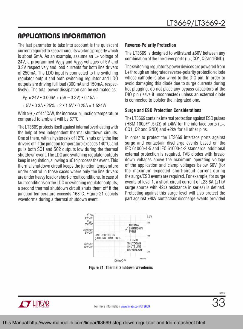
LT3669/LT3669-2
333669f
For more information www.linear.com/LT3669
applicaTions inForMaTionThe last parameter to take into account is the quiescent current required to keep all circuits working properly which is about 6mA. As an example, assume an L+ voltage of 24V, a programmed VOUT and VLDO voltages of 5V and 3.3V respectively and load currents for both line drivers of 250mA. The LDO input is connected to the switching regulator output and both switching regulator and LDO outputs are driving full load (300mA and 150mA, respec-tively). The total power dissipation can be estimated as:
PD = 24V • 0.006A + (5V – 3.3V) • 0.15A +
+ 5V • 0.3A • 25% + 2 • 1.5V • 0.25A = 1.524W
With a θJA of 44°C/W, the increase in junction temperature compared to ambient will be 67°C.
The LT3669 protects itself against internal overheating with the help of two independent thermal shutdown circuits. One of them, with a hysteresis of 12°C, shuts only the line drivers off if the junction temperature exceeds 140°C, and pulls both SC1 and SC2 outputs low during the thermal shutdown event. The LDO and switching regulator outputs keep in regulation, allowing a µC to process the event. This thermal shutdown circuit keeps the junction temperature under control in those cases where only the line drivers are under heavy load or short-circuit conditions. In case of fault conditions on the LDO or switching regulator outputs, a second thermal shutdown circuit shuts them off if the junction temperature exceeds 168°C. Figure 21 depicts waveforms during a thermal shutdown event.
Reverse-Polarity Protection
The LT3669 is designed to withstand ±60V between any combination of the line driver ports (L+, CQ1, Q2 and GND).
The switching regulator’s power devices are powered from L+ through an integrated reverse-polarity protection diode whose cathode is also wired to the DIO pin. In order to avoid damaging this diode due to surge currents during hot plugging, do not place any bypass capacitors at the DIO pin (leave it unconnected) unless an external diode is connected to bolster the integrated one.
Surge and ESD Protection Considerations
The LT3669 contains internal protection against ESD pulses (HBM 100pF/1.5kΩ) of ±4kV for the interface ports (L+, CQ1, Q2 and GND) and ±2kV for all other pins.
In order to protect the LT3669 interface ports against surge and contact/air discharge events based on the IEC 61000-4-5 and IEC 61000-4-2 standards, additional external protection is required. TVS diodes with break-down voltages above the maximum operating voltage of the application and clamp voltages below 60V (for the maximum expected short-circuit current during the surge/ESD event) are required. For example, for surge events of level 1, a short-circuit current of ±23.8A (±1kV surge source with 42Ω resistance in series) is defined. Protecting against this surge level will also protect the part against ±8kV contact/air discharge events provided
Figure 21. Thermal Shutdown Waveforms
100ms/DIV
VLDO5V/DIV
5V
3.3V
0V
0V
VCQ1/Q210V/DIV
VOUT5V/DIV
VSC1/SC25V/DIV
36692 F21
LINE DRIVERS ON(PULLING LOAD HIGH)
THERMAL SHUTDOWN EVENT
THERMAL SHUTDOWN SHUTS LINEDRIVERS OFF
This Manual:http://www.manuallib.com/linear/lt3669-step-down-regulator-and-ldo-datasheet.html
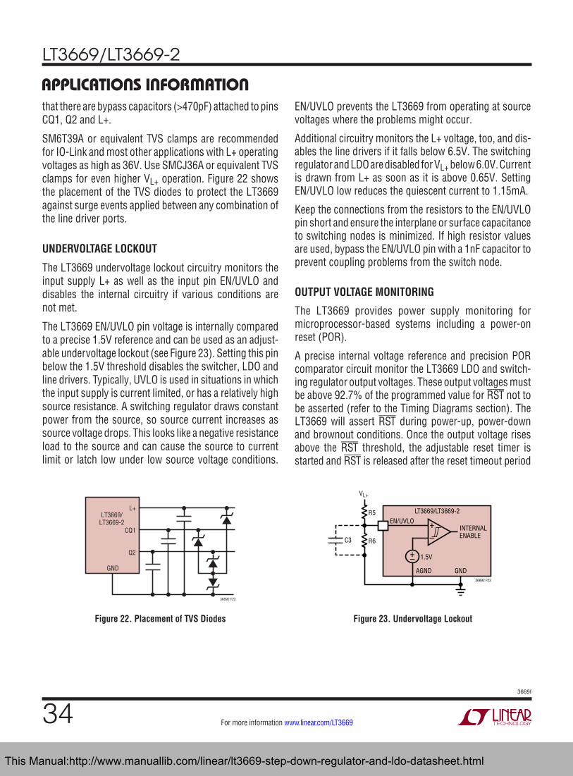
LT3669/LT3669-2
343669f
For more information www.linear.com/LT3669
applicaTions inForMaTionthat there are bypass capacitors (>470pF) attached to pins CQ1, Q2 and L+.
SM6T39A or equivalent TVS clamps are recommended for IO-Link and most other applications with L+ operating voltages as high as 36V. Use SMCJ36A or equivalent TVS clamps for even higher VL+ operation. Figure 22 shows the placement of the TVS diodes to protect the LT3669 against surge events applied between any combination of the line driver ports.
UNDERVOLTAGE LOCKOUT
The LT3669 undervoltage lockout circuitry monitors the input supply L+ as well as the input pin EN/UVLO and disables the internal circuitry if various conditions are not met.
The LT3669 EN/UVLO pin voltage is internally compared to a precise 1.5V reference and can be used as an adjust-able undervoltage lockout (see Figure 23). Setting this pin below the 1.5V threshold disables the switcher, LDO and line drivers. Typically, UVLO is used in situations in which the input supply is current limited, or has a relatively high source resistance. A switching regulator draws constant power from the source, so source current increases as source voltage drops. This looks like a negative resistance load to the source and can cause the source to current limit or latch low under low source voltage conditions.
EN/UVLO prevents the LT3669 from operating at source voltages where the problems might occur.
Additional circuitry monitors the L+ voltage, too, and dis-ables the line drivers if it falls below 6.5V. The switching regulator and LDO are disabled for VL+ below 6.0V. Current is drawn from L+ as soon as it is above 0.65V. Setting EN/UVLO low reduces the quiescent current to 1.15mA.
Keep the connections from the resistors to the EN/UVLO pin short and ensure the interplane or surface capacitance to switching nodes is minimized. If high resistor values are used, bypass the EN/UVLO pin with a 1nF capacitor to prevent coupling problems from the switch node.
OUTPUT VOLTAGE MONITORING
The LT3669 provides power supply monitoring for microprocessor-based systems including a power-on reset (POR).
A precise internal voltage reference and precision POR comparator circuit monitor the LT3669 LDO and switch-ing regulator output voltages. These output voltages must be above 92.7% of the programmed value for RST not to be asserted (refer to the Timing Diagrams section). The LT3669 will assert RST during power-up, power-down and brownout conditions. Once the output voltage rises above the RST threshold, the adjustable reset timer is started and RST is released after the reset timeout period
Figure 22. Placement of TVS Diodes Figure 23. Undervoltage Lockout
+–
1.5V
INTERNALENABLE
36692 F23
LT3669/LT3669-2EN/UVLO
C3
VL+
R5
R6
GNDAGND
+–
L+
36692 F22
GND
LT3669/LT3669-2
Q2
CQ1
This Manual:http://www.manuallib.com/linear/lt3669-step-down-regulator-and-ldo-datasheet.html
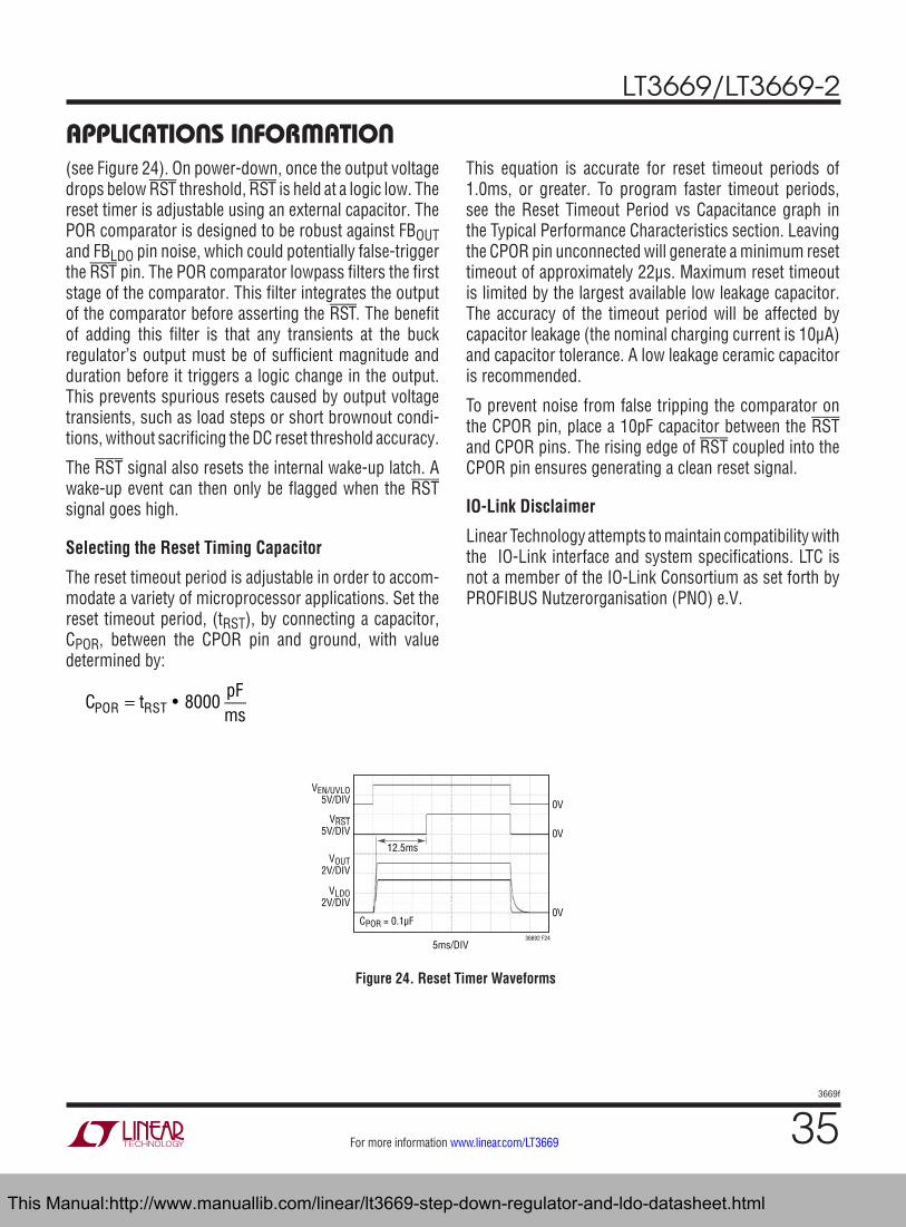
LT3669/LT3669-2
353669f
For more information www.linear.com/LT3669
applicaTions inForMaTion(see Figure 24). On power-down, once the output voltage drops below RST threshold, RST is held at a logic low. The reset timer is adjustable using an external capacitor. The POR comparator is designed to be robust against FBOUT and FBLDO pin noise, which could potentially false-trigger the RST pin. The POR comparator lowpass filters the first stage of the comparator. This filter integrates the output of the comparator before asserting the RST. The benefit of adding this filter is that any transients at the buck regulator’s output must be of sufficient magnitude and duration before it triggers a logic change in the output. This prevents spurious resets caused by output voltage transients, such as load steps or short brownout condi-tions, without sacrificing the DC reset threshold accuracy.
The RST signal also resets the internal wake-up latch. A wake-up event can then only be flagged when the RST signal goes high.
Selecting the Reset Timing Capacitor
The reset timeout period is adjustable in order to accom-modate a variety of microprocessor applications. Set the reset timeout period, (tRST), by connecting a capacitor, CPOR, between the CPOR pin and ground, with value determined by:
CPOR = tRST • 8000
pFms
This equation is accurate for reset timeout periods of 1.0ms, or greater. To program faster timeout periods, see the Reset Timeout Period vs Capacitance graph in the Typical Performance Characteristics section. Leaving the CPOR pin unconnected will generate a minimum reset timeout of approximately 22μs. Maximum reset timeout is limited by the largest available low leakage capacitor. The accuracy of the timeout period will be affected by capacitor leakage (the nominal charging current is 10μA) and capacitor tolerance. A low leakage ceramic capacitor is recommended.
To prevent noise from false tripping the comparator on the CPOR pin, place a 10pF capacitor between the RST and CPOR pins. The rising edge of RST coupled into the CPOR pin ensures generating a clean reset signal.
IO-Link Disclaimer
Linear Technology attempts to maintain compatibility with the IO-Link interface and system specifications. LTC is not a member of the IO-Link Consortium as set forth by PROFIBUS Nutzerorganisation (PNO) e.V.
Figure 24. Reset Timer Waveforms
5ms/DIV
VEN/UVLO5V/DIV 0V
0V
0V
VLDO2V/DIV
VOUT2V/DIV
VRST5V/DIV
36692 F24
12.5ms
CPOR = 0.1µF
This Manual:http://www.manuallib.com/linear/lt3669-step-down-regulator-and-ldo-datasheet.html
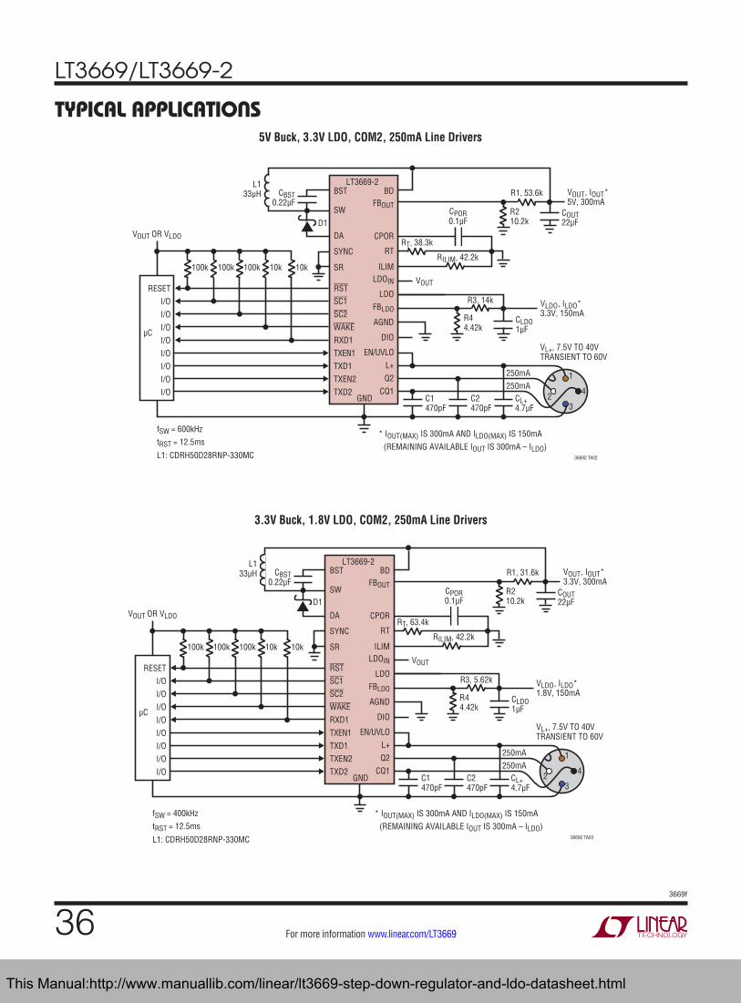
LT3669/LT3669-2
363669f
For more information www.linear.com/LT3669
Typical applicaTions5V Buck, 3.3V LDO, COM2, 250mA Line Drivers
3.3V Buck, 1.8V LDO, COM2, 250mA Line Drivers
RSTSC1SC2WAKERXD1TXEN1TXD1TXEN2TXD2
EN/UVLOL+Q2
CQ1
36692 TA02
GND
SW
DA
BST
SYNC
SR
FBOUT
250mA250mA
23
1
4
CPOR0.1µF
VOUT, IOUT*5V, 300mA
VOUT
COUT22µF
VLDO, ILDO*3.3V, 150mA
VL+, 7.5V TO 40VTRANSIENT TO 60V
LT3669-2
CLDO1µF
L133µH
D1
RT, 38.3k
RILIM, 42.2k
BD R1, 53.6k
R44.42k
C1470pF
C2470pF
CL+4.7µF
RT
CPOR
AGND
FBLDO
LDO
LDOIN
ILIM
DIO
R210.2k
R3, 14k
* IOUT(MAX) IS 300mA AND ILDO(MAX) IS 150mA (REMAINING AVAILABLE IOUT IS 300mA – ILDO)
CBST0.22µF
fSW = 600kHztRST = 12.5ms
L1: CDRH50D28RNP-330MC
VOUT OR VLDO
RESETI/OI/OI/OI/OI/OI/OI/OI/O
µC
100k 100k 100k 10k 10k
RSTSC1SC2WAKERXD1TXEN1TXD1TXEN2TXD2
EN/UVLOL+Q2
CQ1
36692 TA03
GND
SW
DA
BST
SYNC
SR
FBOUT
250mA250mA
23
1
4
CPOR0.1µF
VOUT, IOUT*3.3V, 300mA
VOUT
COUT22µF
VLDO, ILDO*1.8V, 150mA
VL+, 7.5V TO 40VTRANSIENT TO 60V
LT3669-2
CLDO1µF
L133µH
D1
RT, 63.4k
RILIM, 42.2k
BD R1, 31.6k
R44.42k
C1470pF
C2470pF
CL+4.7µF
RT
CPOR
AGND
FBLDO
LDO
LDOIN
ILIM
DIO
R210.2k
R3, 5.62k
* IOUT(MAX) IS 300mA AND ILDO(MAX) IS 150mA (REMAINING AVAILABLE IOUT IS 300mA – ILDO)
CBST0.22µF
fSW = 400kHztRST = 12.5ms
L1: CDRH50D28RNP-330MC
VOUT OR VLDO
RESETI/OI/OI/OI/OI/OI/OI/OI/O
µC
100k 100k 100k 10k 10k
This Manual:http://www.manuallib.com/linear/lt3669-step-down-regulator-and-ldo-datasheet.html
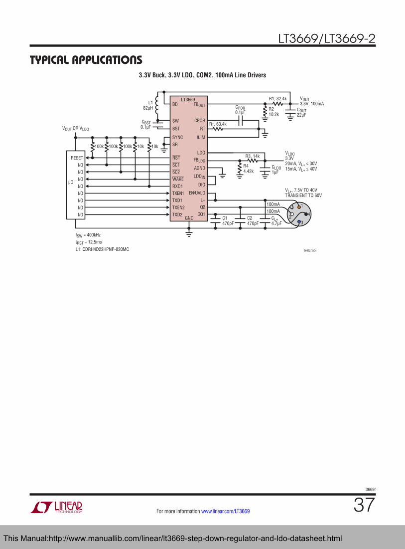
LT3669/LT3669-2
373669f
For more information www.linear.com/LT3669
Typical applicaTions3.3V Buck, 3.3V LDO, COM2, 100mA Line Drivers
RSTSC1SC2WAKERXD1TXEN1TXD1TXEN2TXD2
EN/UVLOL+Q2
CQ1
36692 TA04
GND
SW
BST
SYNC
SR
BD FBOUT
100mA100mA
23
1
4
CPOR0.1µF
VOUT3.3V, 100mA
COUT22µF
VLDO3.3V20mA, VL+ ≤ 30V15mA, VL+ ≤ 40V
VL+, 7.5V TO 40VTRANSIENT TO 60V
LT3669
CLDO1µF
CBST0.1µF
L182µH
RT, 63.4k
R1, 32.4k
R44.42k
C1470pF
C2470pF
CL+4.7µF
RT
CPOR
AGND
FBLDO
LDO
LDOIN
ILIM
DIO
R210.2k
R3, 14k
fSW = 400kHztRST = 12.5ms
L1: CDRH4D22HPNP-820MC
VOUT OR VLDO
RESETI/OI/OI/OI/OI/OI/OI/OI/O
µC
100k 100k 100k 10k 10k
This Manual:http://www.manuallib.com/linear/lt3669-step-down-regulator-and-ldo-datasheet.html
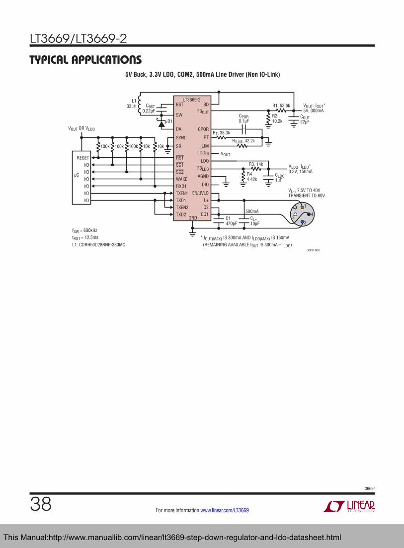
LT3669/LT3669-2
383669f
For more information www.linear.com/LT3669
Typical applicaTions5V Buck, 3.3V LDO, COM2, 500mA Line Driver (Non IO-Link)
36692 TA05
GND
SW
DA
BST
SYNC
SR
FBOUTCPOR0.1µF
VOUT, IOUT*5V, 300mA
VOUT
COUT22µF
VLDO, ILDO*3.3V, 150mA
LT3669-2
CLDO1µF
fSW = 600kHztRST = 12.5ms
L1: CDRH50D28RNP-330MC
L133µH
D1
RT, 38.3k
RILIM, 42.2k
BD R1, 53.6k
R44.42k
RT
CPOR
AGND
FBLDO
LDO
LDOIN
ILIM
DIO
R210.2k
R3, 14k
CBST0.22µF
VOUT OR VLDO
EN/UVLOL+Q2
CQ1500mA
23
1
4
VL+, 7.5V TO 40VTRANSIENT TO 60V
C1470pF
CL+10µF
* IOUT(MAX) IS 300mA AND ILDO(MAX) IS 150mA (REMAINING AVAILABLE IOUT IS 300mA – ILDO)
RSTSC1SC2WAKERXD1TXEN1TXD1TXEN2TXD2
RESETI/OI/OI/OI/OI/OI/O
µC
100k 100k 100k 10k 10k
This Manual:http://www.manuallib.com/linear/lt3669-step-down-regulator-and-ldo-datasheet.html
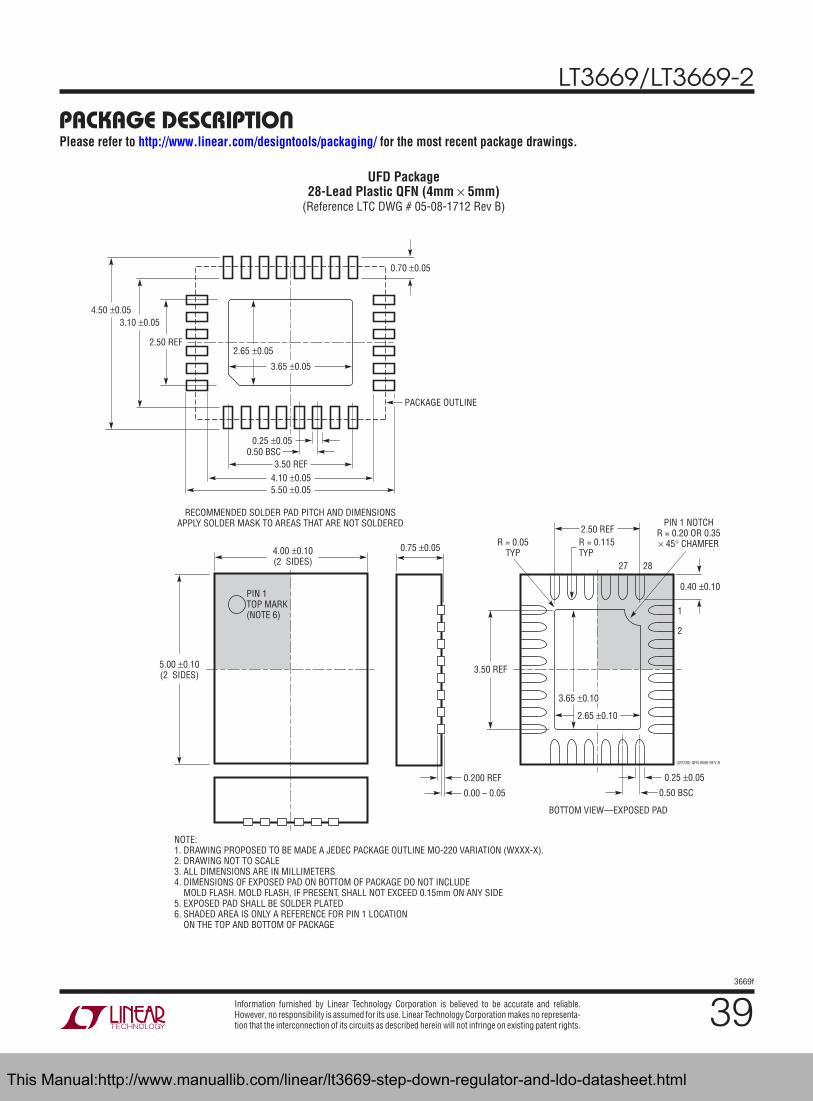
LT3669/LT3669-2
393669f
For more information www.linear.com/LT3669
Information furnished by Linear Technology Corporation is believed to be accurate and reliable. However, no responsibility is assumed for its use. Linear Technology Corporation makes no representa-tion that the interconnection of its circuits as described herein will not infringe on existing patent rights.
package DescripTionPlease refer to http://www.linear.com/designtools/packaging/ for the most recent package drawings.
4.00 ±0.10(2 SIDES)
2.50 REF
5.00 ±0.10(2 SIDES)
NOTE:1. DRAWING PROPOSED TO BE MADE A JEDEC PACKAGE OUTLINE MO-220 VARIATION (WXXX-X).2. DRAWING NOT TO SCALE3. ALL DIMENSIONS ARE IN MILLIMETERS4. DIMENSIONS OF EXPOSED PAD ON BOTTOM OF PACKAGE DO NOT INCLUDE MOLD FLASH. MOLD FLASH, IF PRESENT, SHALL NOT EXCEED 0.15mm ON ANY SIDE5. EXPOSED PAD SHALL BE SOLDER PLATED6. SHADED AREA IS ONLY A REFERENCE FOR PIN 1 LOCATION ON THE TOP AND BOTTOM OF PACKAGE
PIN 1TOP MARK(NOTE 6)
0.40 ±0.10
27 28
1
2
BOTTOM VIEW—EXPOSED PAD
3.50 REF
0.75 ±0.05 R = 0.115TYP
R = 0.05TYP
PIN 1 NOTCHR = 0.20 OR 0.35× 45° CHAMFER
0.25 ±0.05
0.50 BSC
0.200 REF
0.00 – 0.05
(UFD28) QFN 0506 REV B
RECOMMENDED SOLDER PAD PITCH AND DIMENSIONSAPPLY SOLDER MASK TO AREAS THAT ARE NOT SOLDERED
0.70 ±0.05
0.25 ±0.050.50 BSC
2.50 REF
3.50 REF4.10 ±0.055.50 ±0.05
2.65 ±0.05
3.10 ±0.054.50 ±0.05
PACKAGE OUTLINE
2.65 ±0.10
3.65 ±0.10
3.65 ±0.05
UFD Package28-Lead Plastic QFN (4mm × 5mm)
(Reference LTC DWG # 05-08-1712 Rev B)
This Manual:http://www.manuallib.com/linear/lt3669-step-down-regulator-and-ldo-datasheet.html
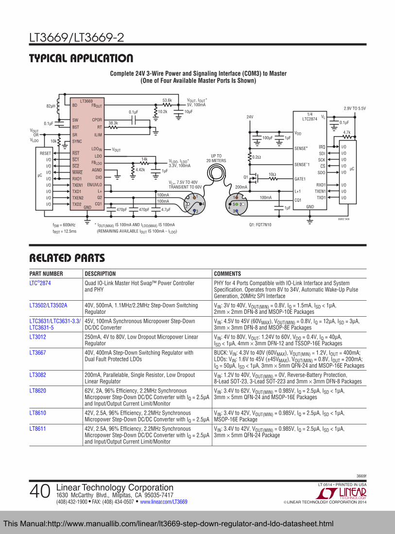
LT3669/LT3669-2
403669f
For more information www.linear.com/LT3669 LINEAR TECHNOLOGY CORPORATION 2014
LT 0514 • PRINTED IN USALinear Technology Corporation1630 McCarthy Blvd., Milpitas, CA 95035-7417(408) 432-1900 ● FAX: (408) 434-0507 ● www.linear.com/LT3669
relaTeD parTs
Typical applicaTionComplete 24V 3-Wire Power and Signaling Interface (COM3) to Master
(One of Four Available Master Ports Is Shown)
1
45 2
3
L+1
CQ1
GATE1
VL
36692 TA06
UP TO20 METERS
24V1/4
LTC2874
2.9V TO 5.5V
IRQSDISCK
CSSDO
RXD1TXEN1
TXD1
I/OI/OI/OI/OI/O
I/OI/OI/O
µCSENSE–1
SENSE+
VDD
GND
100mA
Q1
100µF 1µF
0.1µF
4.7k
10Ω
RSTSC1SC2WAKERXD1TXEN1TXD1TXEN2TXD2
RESETI/OI/OI/OI/OI/OI/OI/OI/O
EN/UVLOL+Q2
CQ1
µC
GND
SW
BST
SR
SYNC
BD FBOUT
100mA100mA
23
1
4
0.1µF
VOUT, IOUT*5V, 100mA
VOUT
10µF
VLDO, ILDO*3.3V, 100mA
VL+, 7.5V TO 40VTRANSIENT TO 60V
LT3669
1µF
fSW = 600kHztRST = 12.5ms
0.1µF
10k
VOUTOR
VLDO
82µH
38.3k
53.6k
4.42k
470pF 470pF 4.7µF
RT
CPOR
AGND
FBLDO
LDO
LDOIN
ILIM
DIO
1µF
10.2k
0.2Ω14k
* IOUT(MAX) IS 100mA AND ILDO(MAX) IS 100mA (REMAINING AVAILABLE IOUT IS 100mA – ILDO)
Q1: FQT7N10
200mA
PART NUMBER DESCRIPTION COMMENTS
LTC®2874 Quad IO-Link Master Hot Swap™ Power Controller and PHY
PHY for 4 Ports Compatible with IO-Link Interface and System Specification. Operates from 8V to 34V, Automatic Wake-Up Pulse Generation, 20MHz SPI Interface
LT3502/LT3502A 40V, 500mA, 1.1MHz/2.2MHz Step-Down Switching Regulator
VIN: 3V to 40V, VOUT(MIN) = 0.8V, IQ = 1.5mA, ISD < 1μA, 2mm × 2mm DFN-8 and MSOP-10E Packages
LTC3631/LTC3631-3.3/ LTC3631-5
45V, 100mA Synchronous Micropower Step-Down DC/DC Converter
VIN: 4.5V to 45V (60VMAX), VOUT(MIN) = 0.8V, IQ = 12μA, ISD = 3μA, 3mm × 3mm DFN-8 and MSOP-8E Packages
LT3012 250mA, 4V to 80V, Low Dropout Micropower Linear Regulator
VIN: 4V to 80V, VOUT: 1.24V to 60V, VDO = 0.4V, IQ = 40μA, ISD < 1μA, 4mm × 3mm DFN-12 and TSSOP-16E Packages
LT3667 40V, 400mA Step-Down Switching Regulator with Dual Fault Protected LDOs
BUCK: VIN: 4.3V to 40V (60VMAX), VOUT(MIN) = 1.2V, IOUT = 400mA; LDOs: VIN: 1.6V to 45V (±45VMAX), VOUT(MIN) = 0.8V, IOUT = 200mA; IQ = 50µA, ISD < 1µA, 3mm × 5mm QFN-24 and MSOP-16E Packages
LT3082 200mA, Parallelable, Single Resistor, Low Dropout Linear Regulator
VIN: 1.2V to 40V, VOUT(MIN) = 0V, Reverse-Battery Protection, 8-Lead SOT-23, 3-Lead SOT-223 and 3mm × 3mm DFN-8 Packages
LT8620 62V, 2A, 96% Efficiency, 2.2MHz Synchronous Micropower Step-Down DC/DC Converter with IQ = 2.5µA and Input/Output Current Limit/Monitor
VIN: 3.4V to 62V, VOUT(MIN) = 0.985V, IQ = 2.5μA, ISD < 1μA, 3mm × 5mm QFN-24 and MSOP-16E Packages
LT8610 42V, 2.5A, 96% Efficiency, 2.2MHz Synchronous Micropower Step-Down DC/DC Converter with IQ = 2.5μA
VIN: 3.4V to 42V, VOUT(MIN) = 0.985V, IQ = 2.5μA, ISD < 1μA, MSOP-16E Package
LT8611 42V, 2.5A, 96% Efficiency, 2.2MHz Synchronous Micropower Step-Down DC/DC Converter with IQ = 2.5μA and Input/Output Current Limit/Monitor
VIN: 3.4V to 42V, VOUT(MIN) = 0.985V, IQ = 2.5μA, ISD < 1μA, 3mm × 5mm QFN-24 Package
This Manual:http://www.manuallib.com/linear/lt3669-step-down-regulator-and-ldo-datasheet.html