Embed Size (px)
Citation preview
LT1815/LT1816/LT1817
1181567fb
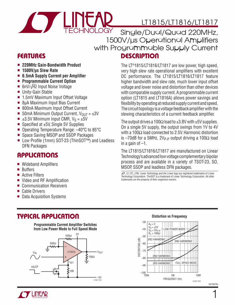
TYPICAL APPLICATION
FEATURES DESCRIPTION
Single/Dual/Quad 220MHz, 1500V/µs Operational Amplifi ers
with Programmable Supply Current
The LT®1815/LT1816/LT1817 are low power, high speed, very high slew rate operational amplifi ers with excellent DC performance. The LT1815/LT1816/LT1817 feature higher bandwidth and slew rate, much lower input offset voltage and lower noise and distortion than other devices with comparable supply current. A programmable current option (LT1815 and LT1816A) allows power savings and fl exibility by operating at reduced supply current and speed. The circuit topology is a voltage feedback amplifi er with the slewing characteristics of a current feedback amplifi er.
The output drives a 100Ω load to ±3.8V with ±5V supplies. On a single 5V supply, the output swings from 1V to 4V with a 100Ω load connected to 2.5V. Harmonic distortion is –70dB for a 5MHz, 2VP-P output driving a 100Ω load in a gain of –1.
The LT1815/LT1816/LT1817 are manufactured on Linear Technology’s advanced low voltage complementary bipolar process and are available in a variety of TSOT-23, SO, MSOP, SSOP and leadless DFN packages.
Programmable Current Amplifi er Switches from Low Power Mode to Full Speed Mode
APPLICATIONS
n 220MHz Gain-Bandwidth Productn 1500V/μs Slew Raten 6.5mA Supply Current per Amplifi ern Programmable Current Optionn 6nV/√Hz Input Noise Voltagen Unity-Gain Stablen 1.5mV Maximum Input Offset Voltagen 8μA Maximum Input Bias Currentn 800nA Maximum Input Offset Currentn 50mA Minimum Output Current, VOUT = ±3Vn ±3.5V Minimum Input CMR, VS = ±5Vn Specifi ed at ±5V, Single 5V Suppliesn Operating Temperature Range: –40°C to 85°Cn Space Saving MSOP and SSOP Packages n Low Profi le (1mm) SOT-23 (ThinSOT™) and Leadless
DFN Packages
n Wideband Amplifi ersn Buffersn Active Filtersn Video and RF Amplifi cationn Communication Receiversn Cable Driversn Data Acquisition Systems
L, LT, LTC, LTM, Linear Technology and the Linear logo are registered trademarks of Linear Technology Corporation. ThinSOT is a trademark of Linear Technology Corporation. All other trademarks are the property of their respective owners.
Distortion vs Frequency
–
+LT1815
40k
100Ω
VOUT
181567 TA01–5V
ISET
500Ω
HS/LP
VIN
500Ω 5V
FREQUENCY (Hz)
–100
–70
–80
–90
–30
–40
–50
–60
181567 TA02
DIST
ORTI
ON (d
B)
100k 10M1M
3RD HARMONIC2ND HARMONIC
LOW POWER MODE
2ND HARMONIC
3RD HARMONIC FULL SPEED MODE
AV = 2VS = ±5VVO = 2VP-PRL = 100Ω
LT1815/LT1816/LT1817
2181567fb
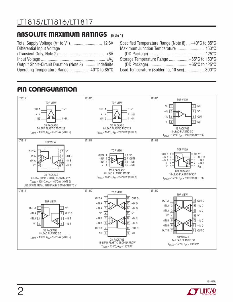
ABSOLUTE MAXIMUM RATINGS
Total Supply Voltage (V+ to V–) ............................. 12.6VDifferential Input Voltage (Transient Only, Note 2) ........................................... ±6VInput Voltage ........................................................... ±VSOutput Short-Circuit Duration (Note 3) .......... Indefi niteOperating Temperature Range .................–40°C to 85°C
(Note 1)
OUT 1
V– 2
TOP VIEW
S5 PACKAGE5-LEAD PLASTIC TSOT-23
+IN3
5 V+
4 –IN+ –
TJMAX = 150°C, θJA = 250°C/W (NOTE 9)
1
2
3
6
5
4
TOP VIEW
S6 PACKAGE6-LEAD PLASTIC TSOT-23
V+
ISET
–IN
OUT
V–
+IN + –
TJMAX = 150°C, θJA = 230°C/W (NOTE 9)
1
2
3
4
8
7
6
5
TOP VIEW
NC
V+
OUT
NC
NC
–IN
+IN
V–
S8 PACKAGE8-LEAD PLASTIC SO
+–
TJMAX = 150°C, θJA = 150°C/W (NOTE 9)
TOP VIEW
DD PACKAGE8-LEAD (3mm × 3mm) PLASTIC DFN
5
6
7
8
9
4
3
2
1OUT A
–IN A
+IN A
V–
V+
OUT B
–IN B
+IN B
A
B
TJMAX = 125°C, θJA = 160°C/W (NOTE 9)UNDERSIDE METAL INTERNALLY CONNECTED TO V–
1234
OUTA–INA+INA
V–
8765
V+
OUTB–INB+INB
TOP VIEW
MS8 PACKAGE8-LEAD PLASTIC MSOP
AB
TJMAX = 150°C, θJA = 250°C/W (NOTE 9)
12345
OUT A–IN A+IN A
V–
V–
109876
V+
OUT B–IN B+IN BISET
TOP VIEW
MS PACKAGE10-LEAD PLASTIC MSOP
AB
TJMAX = 150°C, θJA = 250°C/W (NOTE 9)
1
2
3
4
8
7
6
5
TOP VIEW
V+
OUT B
–IN B
+IN B
OUT A
–IN A
+IN A
V–
S8 PACKAGE8-LEAD PLASTIC SO
A
B
TJMAX = 150°C, θJA = 150°C/W (NOTE 9)GN PACKAGE
16-LEAD PLASTIC SSOP NARROW
1
2
3
4
5
6
7
8
TOP VIEW
16
15
14
13
12
11
10
9
OUT A
–IN A
+IN A
V+
+IN B
–IN B
OUT B
NC
OUT D
–IN D
+IN D
V–
+IN C
–IN C
OUT C
NC
+–
+–
+–
+–
A
B
D
C
TJMAX = 150°C, θJA = 135°C/W
TOP VIEW
S PACKAGE14-LEAD PLASTIC SO
1
2
3
4
5
6
7
14
13
12
11
10
8
8
OUT A
–IN A
+IN A
V+
+IN B
–IN B
OUT B
OUT D
–IN D
+IN D
V–
+IN C
–IN C
OUT C
+–
+
+ +
–
– –
A D
B C
TJMAX = 150°C, θJA = 100°C/W
PIN CONFIGURATIONLT1815 LT1815 LT1815
Specifi ed Temperature Range (Note 8) ....–40°C to 85°CMaximum Junction Temperature ......................... 150°C (DD Package) .................................................... 125°CStorage Temperature Range .................. –65°C to 150°C (DD Package) ..................................... –65°C to 125°CLead Temperature (Soldering, 10 sec)................... 300°C
LT1816 LT1816 LT1816
LT1816 LT1817 LT1817
LT1815/LT1816/LT1817
3181567fb
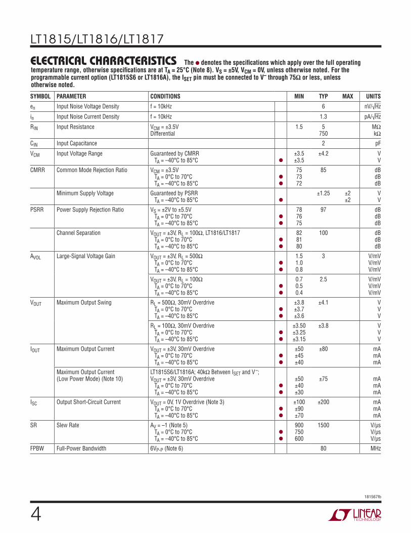
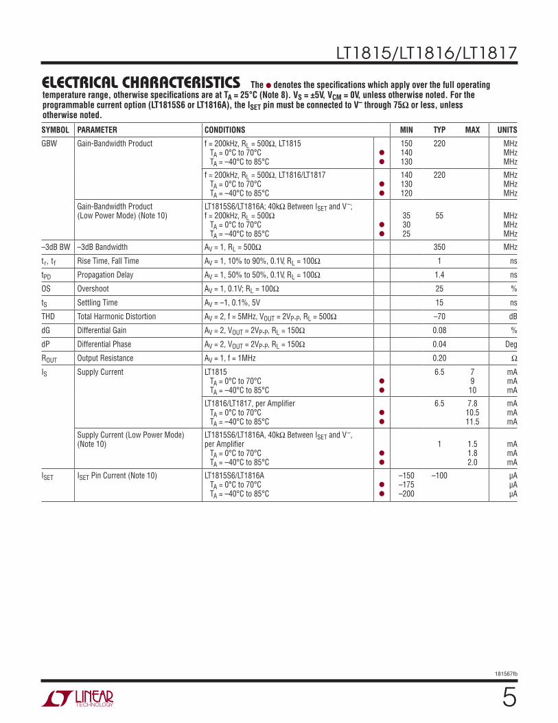
ELECTRICAL CHARACTERISTICS
SYMBOL PARAMETER CONDITIONS MIN TYP MAX UNITS
VOS Input Offset Voltage (Note 4) TA = 0°C to 70°C TA = –40°C to 85°C
l
l
0.2 1.52.03.0
mVmVmV
Input Offset Voltage(Low Power Mode) (Note 10)
LT1815S6/LT1816A, 40kΩ Between ISET and V–
TA = 0°C to 70°C TA = –40°C to 85°C
l
l
2 79
10
mVmVmV
ΔVOS ΔT
Input Offset Voltage Drift TA = 0°C to 70°C (Note 7)TA = –40°C to 85°C (Note 7)
l
l
1010
1530
μV/°C μV/°C
IOS Input Offset CurrentTA = 0°C to 70°CTA = –40°C to 85°C
l
l
60 80010001200
nAnAnA
IB Input Bias CurrentTA = 0°C to 70°CTA = –40°C to 85°C
l
l
–2 ±8±10±12
μAμAμA
The l denotes the specifi cations which apply over the full operating temperature range, otherwise specifi cations are at TA = 25°C (Note 8). VS = ±5V, VCM = 0V, unless otherwise noted. For the programmable current option (LT1815S6 or LT1816A), the ISET pin must be connected to V– through 75Ω or less, unless otherwise noted.
ORDER INFORMATION
LEAD FREE FINISH TAPE AND REEL PART MARKING* PACKAGE DESCRIPTIONSPECIFIEDTEMPERATURE RANGE
LT1815CS5#PBF LT1815CS5#TRPBF LTUP 5-Lead Plastic TSOT-23 0°C to 70°C
LT1815IS5#PBF LT1815IS5#TRPBF LTVC 5-Lead Plastic TSOT-23 –40°C to 85°C
LT1815CS6#PBF LT1815CS6#TRPBF LTUL 6-Lead Plastic TSOT-23 0°C to 70°C
LT1815IS6#PBF LT1815IS6#TRPBF LTVD 6-Lead Plastic TSOT-23 –40°C to 85°C
LT1815CS8#PBF LT1815CS8#TRPBF 1815 8-Lead Plastic SO 0°C to 70°C
LT1815IS8#PBF LT1815IS8#TRPBF 1815I 8-Lead Plastic SO –40°C to 85°C
LT1816CDD#PBF LT1816CDD#TRPBF LAAR 8-Lead (3mm × 3mm) Plastic DFN 0°C to 70°C
LT1816IDD#PBF LT1816IDD#TRPBF LAAR 8-Lead (3mm × 3mm) Plastic DFN –40°C to 150°C
LT1816CMS8#PBF LT1816CMS8#TRPBF LTWA 8-Lead Plastic MSOP 0°C to 70°C
LT1816IMS8#PBF LT1816IMS8#TRPBF LTNQ 8-Lead Plastic MSOP –40°C to 85°C
LT1816ACMS#PBF LT1816ACMS#TRPBF LTYA 10-Lead Plastic MSOP 0°C to 70°C
LT1816AIMS#PBF LT1816AIMS#TRPBF LTXX 10-Lead Plastic MSOP –40°C to 85°C
LT1816CS8#PBF LT1816CS8#TRPBF 1816 8-Lead Plastic SO 0°C to 70°C
LT1816IS8#PBF LT1816IS8#TRPBF 1816I 8-Lead Plastic SO –40°C to 85°C
LT1817CGN#PBF LT1817CGN#TRPBF 1817 16-Lead Plastic SSOP 0°C to 70°C
LT1817IGN#PBF LT1817IGN#TRPBF 1817I 16-Lead Plastic SSOP –40°C to 85°C
LT1817CS#PBF LT1817CS#TRPBF LT1817CS 14-Lead Plastic SO 0°C to 70°C
LT1817IS#PBF LT1817IS#TRPBF LT1817IS 14-Lead Plastic SO –40°C to 85°C
Consult LTC Marketing for parts specifi ed with wider operating temperature ranges. *The temperature grade is identifi ed by a label on the shipping container.Consult LTC Marketing for information on non-standard lead based fi nish parts.For more information on lead free part marking, go to: http://www.linear.com/leadfree/ For more information on tape and reel specifi cations, go to: http://www.linear.com/tapeandreel/
LT1815/LT1816/LT1817
4181567fb
SYMBOL PARAMETER CONDITIONS MIN TYP MAX UNITS
en Input Noise Voltage Density f = 10kHz 6 nV/√Hz
in Input Noise Current Density f = 10kHz 1.3 pA/√Hz
RIN Input Resistance VCM = ±3.5VDifferential
1.5 5750
MΩkΩ
CIN Input Capacitance 2 pF
VCM Input Voltage Range Guaranteed by CMRR TA = –40°C to 85°C l
±3.5±3.5
±4.2 VV
CMRR Common Mode Rejection Ratio VCM = ±3.5V TA = 0°C to 70°C TA = –40°C to 85°C
l
l
757372
85 dBdBdB
Minimum Supply Voltage Guaranteed by PSRR TA = –40°C to 85°C l
±1.25 ±2±2
VV
PSRR Power Supply Rejection Ratio VS = ±2V to ±5.5V TA = 0°C to 70°C TA = –40°C to 85°C
l
l
787675
97 dBdBdB
Channel Separation VOUT = ±3V, RL = 100Ω, LT1816/LT1817 TA = 0°C to 70°C TA = –40°C to 85°C
l
l
828180
100 dBdBdB
AVOL Large-Signal Voltage Gain VOUT = ±3V, RL = 500Ω TA = 0°C to 70°C TA = –40°C to 85°C
l
l
1.51.00.8
3 V/mVV/mVV/mV
VOUT = ±3V, RL = 100Ω TA = 0°C to 70°C TA = –40°C to 85°C
l
l
0.70.50.4
2.5 V/mVV/mVV/mV
VOUT Maximum Output Swing RL = 500Ω, 30mV Overdrive TA = 0°C to 70°C TA = –40°C to 85°C
l
l
±3.8±3.7±3.6
±4.1 VVV
RL = 100Ω, 30mV Overdrive TA = 0°C to 70°C TA = –40°C to 85°C
l
l
±3.50±3.25±3.15
±3.8 VVV
IOUT Maximum Output Current VOUT = ±3V, 30mV Overdrive TA = 0°C to 70°C TA = –40°C to 85°C
l
l
±50±45±40
±80 mAmAmA
Maximum Output Current(Low Power Mode) (Note 10)
LT1815S6/LT1816A; 40kΩ Between ISET and V–;VOUT = ±3V, 30mV Overdrive TA = 0°C to 70°C TA = –40°C to 85°C
l
l
±50±40±30
±75 mAmAmA
ISC Output Short-Circuit Current VOUT = 0V, 1V Overdrive (Note 3) TA = 0°C to 70°C TA = –40°C to 85°C
l
l
±100±90±70
±200 mAmAmA
SR Slew Rate AV = –1 (Note 5) TA = 0°C to 70°C TA = –40°C to 85°C
l
l
900750600
1500 V/μsV/μsV/μs
FPBW Full-Power Bandwidth 6VP-P (Note 6) 80 MHz
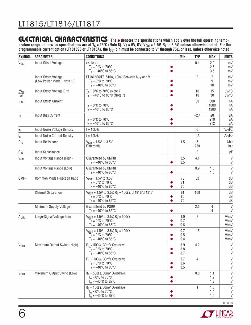
ELECTRICAL CHARACTERISTICS The l denotes the specifi cations which apply over the full operating temperature range, otherwise specifi cations are at TA = 25°C (Note 8). VS = ±5V, VCM = 0V, unless otherwise noted. For the programmable current option (LT1815S6 or LT1816A), the ISET pin must be connected to V– through 75Ω or less, unless otherwise noted.
LT1815/LT1816/LT1817
5181567fb
SYMBOL PARAMETER CONDITIONS MIN TYP MAX UNITS
GBW Gain-Bandwidth Product f = 200kHz, RL = 500Ω, LT1815 TA = 0°C to 70°C TA = –40°C to 85°C
l
l
150140130
220 MHzMHzMHz
f = 200kHz, RL = 500Ω, LT1816/LT1817 TA = 0°C to 70°C TA = –40°C to 85°C
l
l
140130120
220 MHzMHzMHz
Gain-Bandwidth Product(Low Power Mode) (Note 10)
LT1815S6/LT1816A; 40kΩ Between ISET and V–;f = 200kHz, RL = 500Ω TA = 0°C to 70°C TA = –40°C to 85°C
l
l
353025
55 MHzMHzMHz
–3dB BW –3dB Bandwidth AV = 1, RL = 500Ω 350 MHz
tr, t f Rise Time, Fall Time AV = 1, 10% to 90%, 0.1V, RL = 100Ω 1 ns
tPD Propagation Delay AV = 1, 50% to 50%, 0.1V, RL = 100Ω 1.4 ns
OS Overshoot AV = 1, 0.1V; RL = 100Ω 25 %
tS Settling Time AV = –1, 0.1%, 5V 15 ns
THD Total Harmonic Distortion AV = 2, f = 5MHz, VOUT = 2VP-P, RL = 500Ω –70 dB
dG Differential Gain AV = 2, VOUT = 2VP-P, RL = 150Ω 0.08 %
dP Differential Phase AV = 2, VOUT = 2VP-P, RL = 150Ω 0.04 Deg
ROUT Output Resistance AV = 1, f = 1MHz 0.20 Ω
IS Supply Current LT1815 TA = 0°C to 70°C TA = –40°C to 85°C
l
l
6.5 7910
mAmAmA
LT1816/LT1817, per Amplifi er TA = 0°C to 70°C TA = –40°C to 85°C
l
l
6.5 7.810.511.5
mAmAmA
Supply Current (Low Power Mode)(Note 10)
LT1815S6/LT1816A, 40kΩ Between ISET and V–, per Amplifi er TA = 0°C to 70°C TA = –40°C to 85°C
l
l
1 1.51.82.0
mAmAmA
ISET ISET Pin Current (Note 10) LT1815S6/LT1816A TA = 0°C to 70°C TA = –40°C to 85°C
l
l
–150–175–200
–100 μAμA
μA
ELECTRICAL CHARACTERISTICS The l denotes the specifi cations which apply over the full operating temperature range, otherwise specifi cations are at TA = 25°C (Note 8). VS = ±5V, VCM = 0V, unless otherwise noted. For the programmable current option (LT1815S6 or LT1816A), the ISET pin must be connected to V– through 75Ω or less, unless otherwise noted.
LT1815/LT1816/LT1817
6181567fb
ELECTRICAL CHARACTERISTICS The l denotes the specifi cations which apply over the full operating temp-erature range, otherwise specifi cations are at TA = 25°C (Note 8). VS = 5V, OV; VCM = 2.5V, RL to 2.5V, unless otherwise noted. For the programmable current option (LT1815S6 or LT1816A), the ISET pin must be connected to V– through 75Ω or less, unless otherwise noted.
SYMBOL PARAMETER CONDITIONS MIN TYP MAX UNITS
VOS Input Offset Voltage (Note 4) TA = 0°C to 70°C TA = –40°C to 85°C
l
l
0.4 2.02.53.5
mVmVmV
Input Offset Voltage(Low Power Mode) (Note 10)
LT1815S6/LT1816A, 40kΩ Between ISET and V–
TA = 0°C to 70°C TA = –40°C to 85°C
l
l
2 79
10
mVmVmV
ΔVOS ΔT
Input Offset Voltage Drift TA = 0°C to 70°C (Note 7)TA = –40°C to 85°C (Note 7)
l
l
1010
1530
μV/°CμV/°C
IOS Input Offset CurrentTA = 0°C to 70°CTA = –40°C to 85°C
l
l
60 80010001200
nAnAnA
IB Input Bias CurrentTA = 0°C to 70°CTA = –40°C to 85°C
l
l
–2.4 ±8±10±12
μAμAμA
en Input Noise Voltage Density f = 10kHz 6 nV/√Hz
in Input Noise Current Density f = 10kHz 1.3 pA/√Hz
RIN Input Resistance VCM = 1.5V to 3.5VDifferential
1.5 5750
MΩkΩ
CIN Input Capacitance 2 pF
VCM Input Voltage Range (High) Guaranteed by CMRR TA = –40°C to 85°C l
3.53.5
4.1 VV
Input Voltage Range (Low) Guaranteed by CMRR TA = –40°C to 85°C l
0.9 1.51.5
VV
CMRR Common Mode Rejection Ratio VCM = 1.5V to 3.5V TA = 0°C to 70°C TA = –40°C to 85°C
l
l
737170
82 dBdBdB
Channel Separation VOUT = 1.5V to 3.5V, RL = 100Ω, LT1816/LT1817 TA = 0°C to 70°C TA = –40°C to 85°C
l
l
818079
100 dBdBdB
Minimum Supply Voltage Guaranteed by PSRR TA = –40°C to 85°C l
2.5 44
VV
AVOL
Large-Signal Voltage Gain VOUT = 1.5V to 3.5V, RL = 500Ω
TA = 0°C to 70°C TA = –40°C to 85°C
l
l
1.00.70.6
2 V/mVV/mVV/mV
VOUT = 1.5V to 3.5V, RL = 100Ω TA = 0°C to 70°C TA = –40°C to 85°C
l
l
0.70.50.4
1.5 V/mVV/mVV/mV
VOUT Maximum Output Swing (High) RL = 500Ω, 30mV Overdrive TA = 0°C to 70°C TA = –40°C to 85°C
l
l
3.93.83.7
4.2 VVV
RL = 100Ω, 30mV Overdrive TA = 0°C to 70°C TA = –40°C to 85°C
l
l
3.73.63.5
4 VVV
VOUT Maximum Output Swing (Low) RL = 500Ω, 30mV Overdrive TA = 0°C to 70°C TA = –40°C to 85°C
l
l
0.8 1.11.21.3
VVV
RL = 100Ω, 30mV Overdrive TA = 0°C to 70°C TA = –40°C to 85°C
l
l
1 1.31.41.5
VVV
LT1815/LT1816/LT1817
7181567fb
SYMBOL PARAMETER CONDITIONS MIN TYP MAX UNITS
IOUT Maximum Output Current VOUT = 1.5V or 3.5V, 30mV Overdrive TA = 0°C to 70°C TA = –40°C to 85°C
l
l
±30±25±20
±50 mAmAmA
Maximum Output Current(Low Power Mode) (Note 10)
LT1815S6/LT1816A; 40kΩ Between ISET and V–;VOUT = 1.5V or 3.5V, 30mV Overdrive TA = 0°C to 70°C TA = –40°C to 85°C
l
l
±30±25±20
±50 mAmAmA
ISC Output Short-Circuit Current VOUT = 2.5V, 1V Overdrive (Note 3) TA = 0°C to 70°C TA = –40°C to 85°C
l
l
±80±70±50
±140 mAmAmA
SR Slew Rate AV = –1 (Note 5) TA = 0°C to 70°C TA = –40°C to 85°C
l
l
450375300
750 V/μs V/μs V/μs
FPBW Full-Power Bandwidth 2VP-P (Note 6) 120 MHz
GBW Gain-Bandwidth Product f = 200kHz, RL = 500Ω, LT1815TA = 0°C to 70°CTA = –40°C to 85°C
l
l
140130120
200 MHzMHzMHz
f = 200kHz, RL = 500Ω, LT1816/LT1817 TA = 0°C to 70°C TA = –40°C to 85°C
l
l
130110100
200 MHzMHzMHz
Gain-Bandwidth Product(Low Power Mode) (Note 10)
LT1815S6/LT1816A; 40kΩ Between ISET and V–;f = 200kHz, RL = 500Ω TA = 0°C to 70°C TA = –40°C to 85°C
l
l
302520
50 MHzMHzMHz
–3dB BW –3dB Bandwidth AV = 1, RL = 500Ω 300 MHz
tr, t f Rise Time, Fall Time AV = 1, 10% to 90%, 0.1V, RL = 100Ω 1.2 ns
tPD Propagation Delay AV = 1, 50% to 50%, 0.1V, RL = 100Ω 1.5 ns
OS Overshoot AV = 1, 0.1V; RL = 100Ω 25 %
tS Settling Time AV = –1, 0.1%, 2V 15 ns
THD Total Harmonic Distortion AV = 2, f = 5MHz, VOUT = 2VP-P, RL = 500Ω –65 dB
dG Differential Gain AV = 2, VOUT = 2VP-P, RL = 150Ω 0.08 %
dP Differential Phase AV = 2, VOUT = 2VP-P, RL = 150Ω 0.13 Deg
ROUT Output Resistance AV = 1, f = 1MHz 0.24 Ω
IS Supply Current LT1815 TA = 0°C to 70°C TA = –40°C to 85°C
l
l
6.3 81011
mAmAmA
LT1816/LT1817, per Amplifi er TA = 0°C to 70°C TA = –40°C to 85°C
l
l
6.3 91213
mAmAmA
Supply Current (Low Power Mode)(Note 10)
LT1815S6/LT1816A, 40kΩ Between ISET and V–, per Amplifi er TA = 0°C to 70°C TA = –40°C to 85°C
l
l
0.9 1.51.82.0
mAmAmA
ISET ISET Pin Current (Note 10) LT1815S6/LT1816A TA = 0°C to 70°C TA = –40°C to 85°C
l
l
–150–175–200
–100 μAμA
μA
ELECTRICAL CHARACTERISTICS The l denotes the specifi cations which apply over the full operating temp-erature range, otherwise specifi cations are at TA = 25°C (Note 8). VS = 5V, OV; VCM = 2.5V, RL to 2.5V, unless otherwise noted. For the programmable current option (LT1815S6 or LT1816A), the ISET pin must be connected to V– through 75Ω or less, unless otherwise noted.
Note 1: Stresses beyond those listed under Absolute Maximum Ratings may cause permanent damage to the device. Exposure to any Absolute Maximum Rating condition for extended periods may affect device reliability and lifetime.
Note 2: Differential inputs of ±6V are appropriate for transient operation only, such as during slewing. Large sustained differential inputs can cause excessive power dissipation and may damage the part.
LT1815/LT1816/LT1817
8181567fb
Note 3: A heat sink may be required to keep the junction temperature below absolute maximum when the output is shorted indefi nitely.Note 4: Input offset voltage is pulse tested and is exclusive of warm-up drift.Note 5: Slew rate is measured between ±2V at the output with ±3V input for ±5V supplies and 2VP-P at the output with a 3VP-P input for single 5V supplies.Note 6: Full-power bandwidth is calculated from the slew rate: FPBW = SR/2πVP
Note 7: This parameter is not 100% tested.Note 8: The LT1815C/LT1816C/LT1817C are guaranteed to meet specifi ed performance from 0°C to 70°C and are designed, characterized and
expected to meet the extended temperature limits, but are not tested at –40°C and 85°C. The LT1815I/LT1816I/LT1817I are guaranteed to meet the extended temperature limits.Note 9: Thermal resistance (θJA) varies with the amount of PC board metal connected to the package. The specifi ed values are for short traces connected to the leads. If desired, the thermal resistance can be substantially reduced by connecting Pin 2 of the TSOT-23, Pin 4 of the SO-8 and MS8, Pin 5 of the MS10 or the underside metal of the DD package to a large metal area.Note 10: A resistor of 40k or less is required between the ISET and V– pins of the LT1815S6 and the LT1816AMS. See the Applications Information section for information on selecting a suitable resistor.
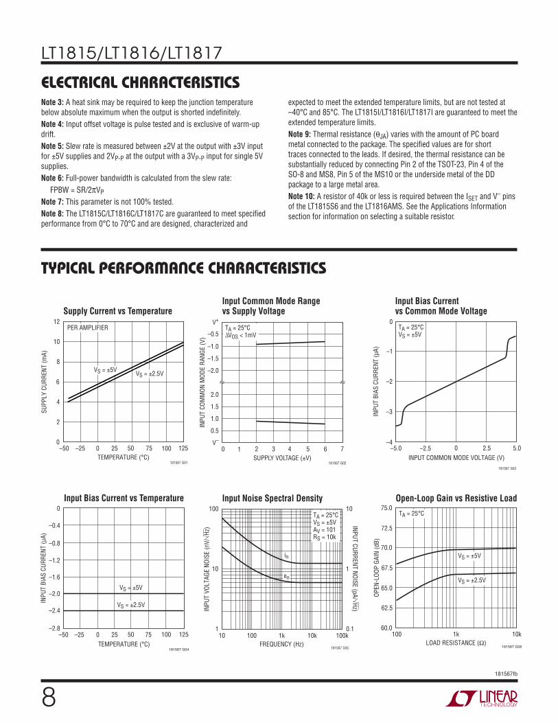
ELECTRICAL CHARACTERISTICS
Supply Current vs TemperatureInput Common Mode Rangevs Supply Voltage
Input Bias Currentvs Common Mode Voltage
Input Bias Current vs Temperature Input Noise Spectral Density Open-Loop Gain vs Resistive Load
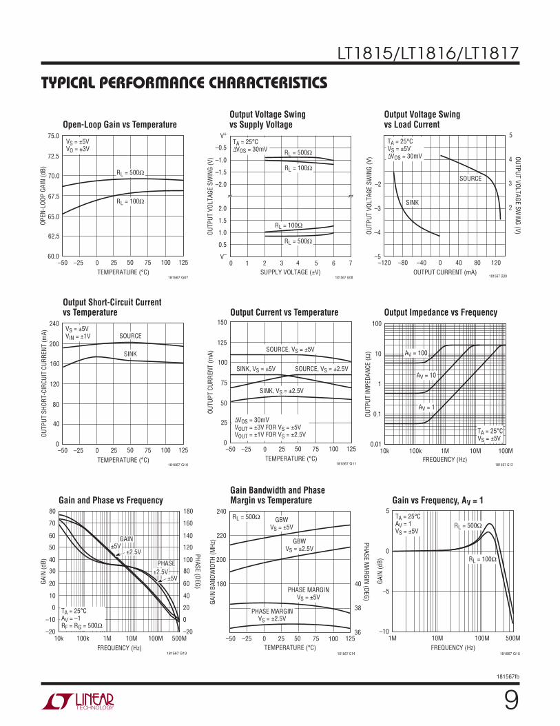
TYPICAL PERFORMANCE CHARACTERISTICS
TEMPERATURE (°C)–50 –25
0
SUPP
LY C
URRE
NT (m
A)
4
12
10
0 50 75
181567 G01
2
8
6
25 100 125
VS = ±5V VS = ±2.5V
PER AMPLIFIER
SUPPLY VOLTAGE (±V)0
V–
INPU
T CO
MM
ON M
ODE
RANG
E (V
)
1.0
1.5
2.0
V+
–2.0
–1.5
2 4 5
181567 G02
0.5
–1.0
–0.5
1 3 6 7
TA = 25°CΔVOS < 1mV
INPUT COMMON MODE VOLTAGE (V)–5.0
INPU
T BI
AS C
URRE
NT (μ
A)–2
–1
TA = 25°CVS = ±5V
5.0
181567 G03
–3
–4–2.5 0 2.5
0
TEMPERATURE (°C)–50
–1.2
–0.8
0
25 75
181567 G04
–1.6
–2.0
–25 0 50 100 125
–2.4
–2.8
–0.4
INPU
T BI
AS C
URRE
NT (μ
A)
VS = ±5V
VS = ±2.5V
FREQUENCY (Hz)10 100
1
10
in
100
0.1
1
10
1k 10k 100k
181567 G05
TA = 25°CVS = ±5VAV = 101RS = 10k
en
INPU
T VO
LTAG
E NO
ISE
(nV/
Hz) INPUT CURRENT NOISE (pA/
Hz)
LOAD RESISTANCE (Ω)100
60.0
OPEN
-LOO
P GA
IN (d
B)
62.5
65.0
67.5
70.0
75.0
1k 10k
181567 G06
72.5
TA = 25°C
VS = ±5V
VS = ±2.5V
LT1815/LT1816/LT1817
9181567fb
TYPICAL PERFORMANCE CHARACTERISTICS
Output Short-Circuit Currentvs Temperature Output Current vs Temperature Output Impedance vs Frequency
Gain and Phase vs FrequencyGain Bandwidth and Phase Margin vs Temperature Gain vs Frequency, AV = 1
Open-Loop Gain vs TemperatureOutput Voltage Swingvs Supply Voltage
Output Voltage Swing vs Load Current
TEMPERATURE (°C)–50
OPEN
-LOO
P GA
IN (d
B)
70.0
72.5
75.0
25 75
181567 G07
67.5
65.0
–25 0 50 100 125
62.5
60.0
VS = ±5VVO = ±3V
RL = 500Ω
RL = 100Ω
SUPPLY VOLTAGE (±V)0
V–
OUTP
UT V
OLTA
GE S
WIN
G (V
)
1.0
1.5
2.0
V+
–2.0
–1.5
2 4 5
181567 G08
0.5
–1.0
–0.5
1 3 6 7
TA = 25°CΔVOS = 30mV
RL = 100Ω
RL = 100Ω
RL = 500Ω
RL = 500Ω
OUTPUT CURRENT (mA)–120
OUTP
UT V
OLTA
GE S
WIN
G (V
) OUTPUT VOLTAGE SWING (V)
–2
40
181567 G09
–3
–4
–5
5
4
3
2
–80 –40 0 80 120
TA = 25°CVS = ±5VΔVOS = 30mV
SINK
SOURCE
TEMPERATURE (°C)–50
OUTP
UT S
HORT
-CIR
CUIT
CUR
RENT
(mA)
160
200
240
25 75
181567 G10
120
80
–25 0 50 100 125
40
0
SOURCE
SINK
VS = ±5VVIN = ±1V
TEMPERATURE (°C)–50
OUTU
PT C
URRE
NT (m
A)
100
125
150
25 75
181567 G11
75
50
–25 0 50 100 125
25
0
ΔVOS = 30mVVOUT = ±3V FOR VS = ±5VVOUT = ±1V FOR VS = ±2.5V
SOURCE, VS = ±5V
SINK, VS = ±5V SOURCE, VS = ±2.5V
SINK, VS = ±2.5V
FREQUENCY (Hz)
0.01
OUTP
UT IM
PEDA
NCE
(Ω)
0.1
100
1M100k10k 10M 100M
181567 G12
1
10 AV = 100
AV = 10
AV = 1
TA = 25°CVS = ±5V
FREQUENCY (Hz)10k
20GAIN
(dB)
PHASE (DEG)
30
40
50
60
100k 1M 500M100M10M
181567 G13
10
0
–10
–20
70
80
60
80
100
120
140
40
20
0
–20
160
180
TA = 25°CAV = –1RF = RG = 500Ω
±2.5V
±2.5V
±5V
±5V
GAIN
PHASE
TEMPERATURE (°C)–50 –25
GAIN
BAN
DWID
TH (M
Hz) PHASE M
ARGIN (DEG)
180
240
0 50 75
181567 G14
36
40
38
220
200
25 100 125
GBWVS = ±5V
GBWVS = ±2.5V
PHASE MARGINVS = ±2.5V
PHASE MARGINVS = ±5V
RL = 500Ω
FREQUENCY (Hz)1M
GAIN
(dB)
–5
0
10M 100M 500M
181567 G15
–10
5TA = 25°CAV = 1VS = ±5V
RL = 500Ω
RL = 100Ω
LT1815/LT1816/LT1817
10181567fb
TYPICAL PERFORMANCE CHARACTERISTICS
Power Supply Rejection Ratiovs Frequency
Common Mode Rejection Ratiovs Frequency
Supply Current vs Programming Resistor
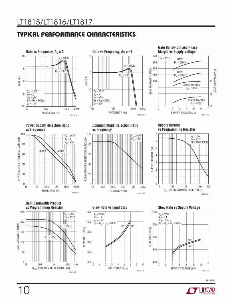
Gain Bandwidth Product vs Programming Resistor Slew Rate vs Input Step Slew Rate vs Supply Voltage
Gain vs Frequency, AV = 2 Gain vs Frequency, AV = –1Gain Bandwidth and Phase Margin vs Supply Voltage
FREQUENCY (Hz)1M
GAIN
(dB)
10M 100M 300M
181567 G16
5
0
–5
–10
10
TA = 25°CAV = 2VS = ±5VRF = RG = 500ΩCF = 1pF
RL = 500Ω
RL = 100Ω
FREQUENCY (Hz)1M
GAIN
(dB)
–5
0
10M 100M 300M
181567 G17
–10
5
TA = 25°CAV = –1VS = ±5VRF = RG = 500ΩCF = 1pF
RL = 500Ω
RL = 100Ω
SUPPLY VOLTAGE (±V)0
GAIN
BAN
DWID
TH (M
Hz) PHASE M
ARGIN (DEG)
3
181567 G18
160 45
40
351 2 4
240
200
220
180
5 6 7
TA = 25°C GBWRL = 500Ω
GBWRL = 100Ω
PHASE MARGINRL = 100Ω
PHASE MARGINRL = 500Ω
FREQUENCY (Hz)1k 10k 100k
40
POW
ER S
UPPL
Y RE
JECT
ION
RATI
O (d
B)
60
80
1M 10M 100M
181567 G19
20
0
100
–PSRR+PSRR
TA = 25°CAV = 1VS = ±5V
FREQUENCY (Hz)1k 10k 100k
40
COM
MON
MOD
E RE
JECT
ION
RATI
O (d
B)
60
80
1M 10M 100M
181567 G20
20
0
100TA = 25°CVS = ±5V
RSET PROGRAMMING RESISTOR (Ω)
2SUPP
LY C
URRE
NT (m
A)4
6
7
10 1k 10k 40k
181567 G21
0100
5
3
1
VS = ±5VTA = 25°CPER AMPLIFIER
RSET PROGRAMING RESISTOR (Ω)
50
GAIN
BAN
DWID
TH (M
Hz)
100
150
200
250
10 1k 10k 40k
181567 G22
0100
VS = ±5VTA = 25°C
RL = 500Ω
RL = 100Ω
INPUT STEP (VP-P)0
300
SLEW
RAT
E (V
/μs)
900
1800
2 4 5
181567 G23
600
1500
1200
1 3 6 7 8
TA =25°CAV = –1VS = ±5VRF = RG = RL = 500Ω
SR–SR+
SUPPLY VOLTAGE (±V)0
400
SLEW
RAT
E (V
/μs)
600
2 4 5
181567 G24
800
1000
1200
1 3 6 7
TA =25°CAV = –1VIN = 2VP-PRF = RG = RL = 500Ω
SR+
SR–
LT1815/LT1816/LT1817
11181567fb
181567 G30
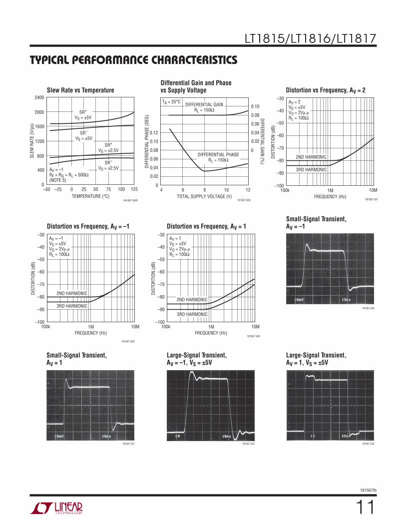
TYPICAL PERFORMANCE CHARACTERISTICS
Distortion vs Frequency, AV = –1 Distortion vs Frequency, AV = 1Small-Signal Transient,AV = –1
Small-Signal Transient,AV = 1
Large-Signal Transient,AV = –1, VS = ±5V
Large-Signal Transient,AV = 1, VS = ±5V
Slew Rate vs TemperatureDifferential Gain and Phasevs Supply Voltage Distortion vs Frequency, AV = 2
TEMPERATURE (°C)–50
SLEW
RAT
E (V
/μs) 1600
2000
2400
25 75
181567 G25
1200
800
–25 0 50 100 125
400
0
SR+
VS = ±5V
SR–
VS = ±5VSR+
VS = ±2.5V
SR–
VS = ±2.5VAV = –1RF = RG = RL = 500Ω(NOTE 5)
TOTAL SUPPLY VOLTAGE (V)4
0
DIFF
EREN
TIAL
PHA
SE (D
EG) DIFFERENTIAL GAIN (%
)
0.02
0.06
0.08
0.10
6 8
181567 G26
0.04
0.12
0
0.02
0.06
0.08
0.10
0.04
TA = 25°C
10 12
DIFFERENTIAL GAINRL = 150Ω
DIFFERENTIAL PHASERL = 150Ω
FREQUENCY (Hz)
–100
–70
–80
–90
–30
–40
–50
–60
181567 G27
DIST
ORTI
ON (d
B)
100k 10M1M
2ND HARMONIC
3RD HARMONIC
AV = 2VS = ±5VVO = 2VP-PRL = 100Ω
FREQUENCY (Hz)
–100
–70
–80
–90
–30
–40
–50
–60
181567 G28
DIST
ORTI
ON (d
B)
100k 10M1M
2ND HARMONIC
3RD HARMONIC
AV = –1VS = ±5VVO = 2VP-PRL = 100Ω
FREQUENCY (Hz)
–100
–70
–80
–90
–30
–40
–50
–60
181567 G29
DIST
ORTI
ON (d
B)
100k 10M1M
2ND HARMONIC
3RD HARMONIC
AV = 1VS = ±5VVO = 2VP-PRL = 100Ω
181567 G33181567 G32181567 G31
LT1815/LT1816/LT1817
12181567fb
Layout and Passive Components
As with all high speed amplifi ers, the LT1815/LT1816/LT1817 require some attention to board layout. A ground plane is recommended and trace lengths should be mini-mized, especially on the negative input lead.
Low ESL/ESR bypass capacitors should be placed directly at the positive and negative supply (0.01μF ceramics are recommended). For high drive current applications, ad-ditional 1μF to 10μF tantalums should be added.
The parallel combination of the feedback resistor and gain setting resistor on the inverting input combine with the input capacitance to form a pole that can cause peaking or even oscillations. If feedback resistors greater than 1k are used, a parallel capacitor of value:
CF > RG • CIN/RF
should be used to cancel the input pole and optimize dy-namic performance. For applications where the DC noise gain is 1 and a large feedback resistor is used, CF should be greater than or equal to CIN. An example would be an I-to-V converter.
Input Considerations
The inputs of the LT1815/LT1816/LT1817 amplifi ers are connected to the base of an NPN and PNP bipolar transis-tor in parallel. The base currents are of opposite polarity and provide fi rst-order bias current cancellation. Due to variation in the matching of NPN and PNP beta, the polar-ity of the input bias current can be positive or negative. The offset current, however, does not depend on beta matching and is tightly controlled. Therefore, the use of balanced source resistance at each input is recommended for applications where DC accuracy must be maximized. For example, with a 100Ω source resistance at each input, the 800nA maximum offset current results in only 80μV of extra offset, while without balance the 8μA maximum input bias current could result in a 0.8mV offset contribution.
The inputs can withstand differential input voltages of up to 6V without damage and without needing clamping or series resistance for protection. This differential input voltage generates a large internal current (up to 80mA), which results in the high slew rate. In normal transient
APPLICATIONS INFORMATION
closed-loop operation, this does not increase power dis-sipation signifi cantly because of the low duty cycle of the transient inputs. Sustained differential inputs, however, will result in excessive power dissipation and therefore this device should not be used as a comparator.
Capacitive Loading
The LT1815/LT1816/LT1817 are optimized for high band-width and low distortion applications. They can drive a capacitive load of 10pF in a unity-gain confi guration and more with higher gain. When driving a larger capacitive load, a resistor of 10Ω to 50Ω should be connected be-tween the output and the capacitive load to avoid ringing or oscillation. The feedback should still be taken from the output so that the resistor will isolate the capacitive load to ensure stability.
Slew Rate
The slew rate of the LT1815/LT1816/LT1817 is propor-tional to the differential input voltage. Therefore, highest slew rates are seen in the lowest gain confi gurations. For example, a 5V output step in a gain of 10 has a 0.5V input step, whereas in unity gain there is a 5V input step. The LT1815/LT1816/LT1817 are tested for a slew rate in a gain of –1. Lower slew rates occur in higher gain confi gurations.
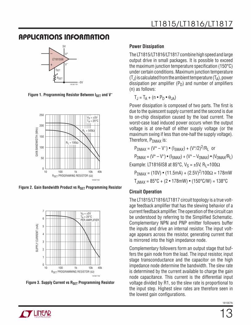
Programmable Supply Current(LT1815/LT1816A)
In order to operate the LT1815S6 or LT1816A at full speed (and full supply current), connect the ISET pin to the nega-tive supply through a resistance of 75Ω or less.
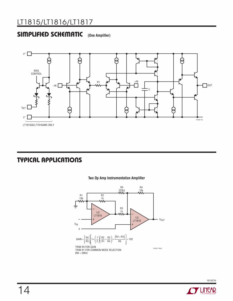
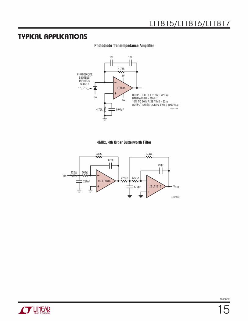
To adjust or program the supply current and speed of the LT1815S6 or LT1816A, connect an external resistor (RSET) between the ISET pin and the negative supply, as shown in Figure 1. The amplifi ers are fully functional with 0 ≤ RSET ≤ 40k. Figures 2 and 3 show how the gain bandwidth and supply current vary with the value of the programming resistor RSET. In addition, the Electrical Characteristics sec-tion of the data sheet specifi es maximum supply current and offset voltage, as well as minimum gain bandwidth and output current at the maximum RSET value of 40k.
LT1815/LT1816/LT1817
13181567fb
APPLICATIONS INFORMATION
Power Dissipation
The LT1815/LT1816/LT1817 combine high speed and large output drive in small packages. It is possible to exceed the maximum junction temperature specifi cation (150°C) under certain conditions. Maximum junction temperature (TJ) is calculated from the ambient temperature (TA), power dissipation per amplifi er (PD) and number of amplifi ers (n) as follows:
TJ = TA + (n • PD • θJA)
Power dissipation is composed of two parts. The fi rst is due to the quiescent supply current and the second is due to on-chip dissipation caused by the load current. The worst-case load induced power occurs when the output voltage is at one-half of either supply voltage (or the maximum swing if less than one-half the supply voltage). Therefore, PDMAX is:
PDMAX = (V+ – V–) • (ISMAX) + (V+/2)2/RL or
PDMAX = (V+ – V–) • (ISMAX) + (V+ – VOMAX) • (VOMAX/RL)
Example: LT1816IS8 at 85°C, VS = ±5V, RL=100Ω
PDMAX = (10V) • (11.5mA) + (2.5V)2/100Ω = 178mW
TJMAX = 85°C + (2 • 178mW) • (150°C/W) = 138°C
Circuit Operation
The LT1815/LT1816/LT1817 circuit topology is a true volt-age feedback amplifi er that has the slewing behavior of a current feedback amplifi er. The operation of the circuit can be understood by referring to the Simplifi ed Schematic. Complementary NPN and PNP emitter followers buffer the inputs and drive an internal resistor. The input volt-age appears across the resistor, generating current that is mirrored into the high impedance node.
Complementary followers form an output stage that buf-fers the gain node from the load. The input resistor, input stage transconductance and the capacitor on the high impedance node determine the bandwidth. The slew rate is determined by the current available to charge the gain node capacitance. This current is the differential input voltage divided by R1, so the slew rate is proportional to the input step. Highest slew rates are therefore seen in the lowest gain confi gurations.
Figure 1. Programming Resistor Between ISET and V–
Figure 2. Gain Bandwidth Product vs RSET Programming Resistor
Figure 3. Supply Current vs RSET Programming Resistor
ISET
V–
181567 F01
V+
RSET
–5V
5V
–
+LT1815S6
RSET PROGRAMING RESISTOR (Ω)
50
GAIN
BAN
DWID
TH (M
Hz)
100
150
200
250
10 1k 10k 40k
181567 F02
0100
VS = 5VTA = 25°C
RL = 500Ω
RL = 100Ω
RSET PROGRAMMING RESISTOR (Ω)
2SUPP
LY C
URRE
NT (m
A)
4
6
7
10 1k 10k 40k
181567 F03
0100
5
3
1
VS = ±5VTA = 25°CPER AMPLIFIER
LT1815/LT1816/LT1817
14181567fb
Two Op Amp Instrumentation Amplifi er
181567 TA03
VIN
TRIM R5 FOR GAINTRIM R1 FOR COMMON MODE REJECTIONBW = 2MHz
R110k
R21k
R5220Ω
R410k
R31k
VOUT
+
––
+
–
+ 1/2LT1816
1/2LT1816
GAIN RR
RR
RR
R R
R43
1 12
21
34
2 3
5102
SIMPLIFIED SCHEMATIC
181567 SS
OUT+IN
–IN
BIASCONTROL
V+
V–
LT1815S6/LT1816AMS ONLY
ISET
R1
C
(One Amplifi er)
TYPICAL APPLICATIONS
LT1815/LT1816/LT1817
15181567fb
TYPICAL APPLICATIONSPhotodiode Transimpedance Amplifi er
4MHz, 4th Order Butterworth Filter
–
+LT1815
4.75k
1pF 1pF
–5V
PHOTODIODESIEMENS/INFINEONSFH213
–5V
181567 TA04
5V
0.01μF
OUTPUT OFFSET ≤1mV TYPICALBANDWIDTH = 30MHz10% TO 90% RISE TIME = 22nsOUTPUT NOISE (20MHz BW) = 300μVP-P
4.75k
–
+1/2 LT1816220pF
VIN665Ω
232Ω
47pF
232Ω
–
+1/2 LT1816470pF
181567 TA05
VOUT
562Ω
274Ω
22pF
274Ω
LT1815/LT1816/LT1817
16181567fb
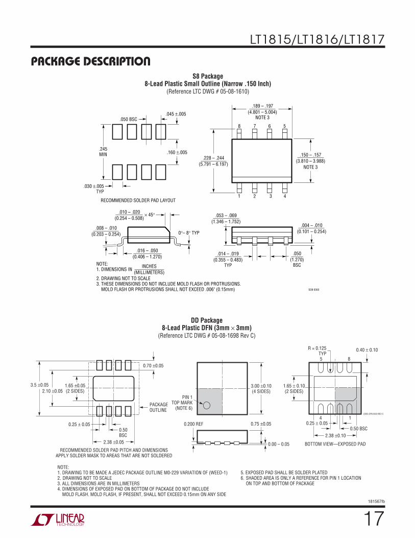
PACKAGE DESCRIPTIONS5 Package
5-Lead Plastic TSOT-23(Reference LTC DWG # 05-08-1635)
S6 Package6-Lead Plastic TSOT-23
(Reference LTC DWG # 05-08-1636)
1.50 – 1.75(NOTE 4)2.80 BSC
0.30 – 0.45 TYP 5 PLCS (NOTE 3)
DATUM ‘A’
0.09 – 0.20 (NOTE 3)S5 TSOT-23 0302 REV B
PIN ONE
2.90 BSC(NOTE 4)
0.95 BSC
1.90 BSC
0.80 – 0.90
1.00 MAX0.01 – 0.100.20 BSC
0.30 – 0.50 REF
NOTE:1. DIMENSIONS ARE IN MILLIMETERS2. DRAWING NOT TO SCALE3. DIMENSIONS ARE INCLUSIVE OF PLATING
4. DIMENSIONS ARE EXCLUSIVE OF MOLD FLASH AND METAL BURR5. MOLD FLASH SHALL NOT EXCEED 0.254mm6. JEDEC PACKAGE REFERENCE IS MO-193
3.85 MAX
0.62 MAX 0.95 REF
RECOMMENDED SOLDER PAD LAYOUTPER IPC CALCULATOR
1.4 MIN2.62 REF
1.22 REF
1.50 – 1.75(NOTE 4)
2.80 BSC
0.30 – 0.45 6 PLCS (NOTE 3)
DATUM ‘A’
0.09 – 0.20 (NOTE 3)S6 TSOT-23 0302 REV B
2.90 BSC(NOTE 4)
0.95 BSC
1.90 BSC
0.80 – 0.90
1.00 MAX0.01 – 0.10
0.20 BSC
0.30 – 0.50 REF
PIN ONE ID
NOTE:1. DIMENSIONS ARE IN MILLIMETERS2. DRAWING NOT TO SCALE3. DIMENSIONS ARE INCLUSIVE OF PLATING
4. DIMENSIONS ARE EXCLUSIVE OF MOLD FLASH AND METAL BURR5. MOLD FLASH SHALL NOT EXCEED 0.254mm6. JEDEC PACKAGE REFERENCE IS MO-193
3.85 MAX
0.62 MAX 0.95 REF
RECOMMENDED SOLDER PAD LAYOUTPER IPC CALCULATOR
1.4 MIN2.62 REF
1.22 REF
LT1815/LT1816/LT1817
17181567fb
PACKAGE DESCRIPTION
DD Package8-Lead Plastic DFN (3mm × 3mm)
(Reference LTC DWG # 05-08-1698 Rev C)
S8 Package8-Lead Plastic Small Outline (Narrow .150 Inch)
(Reference LTC DWG # 05-08-1610)
.016 – .050(0.406 – 1.270)
.010 – .020(0.254 – 0.508)
× 45°�
0°– 8° TYP.008 – .010
(0.203 – 0.254)
SO8 0303
.053 – .069(1.346 – 1.752)
.014 – .019(0.355 – 0.483)
TYP
.004 – .010(0.101 – 0.254)
.050(1.270)
BSC
1 2 3 4
.150 – .157(3.810 – 3.988)
NOTE 3
8 7 6 5
.189 – .197(4.801 – 5.004)
NOTE 3
.228 – .244(5.791 – 6.197)
.245MIN .160 ±.005
RECOMMENDED SOLDER PAD LAYOUT
.045 ±.005 .050 BSC
.030 ±.005 TYP
INCHES(MILLIMETERS)
NOTE:1. DIMENSIONS IN
2. DRAWING NOT TO SCALE3. THESE DIMENSIONS DO NOT INCLUDE MOLD FLASH OR PROTRUSIONS. MOLD FLASH OR PROTRUSIONS SHALL NOT EXCEED .006" (0.15mm)
3.00 0.10(4 SIDES)
NOTE:1. DRAWING TO BE MADE A JEDEC PACKAGE OUTLINE M0-229 VARIATION OF (WEED-1)2. DRAWING NOT TO SCALE3. ALL DIMENSIONS ARE IN MILLIMETERS4. DIMENSIONS OF EXPOSED PAD ON BOTTOM OF PACKAGE DO NOT INCLUDE MOLD FLASH. MOLD FLASH, IF PRESENT, SHALL NOT EXCEED 0.15mm ON ANY SIDE
5. EXPOSED PAD SHALL BE SOLDER PLATED6. SHADED AREA IS ONLY A REFERENCE FOR PIN 1 LOCATION ON TOP AND BOTTOM OF PACKAGE
0.40 0.10
BOTTOM VIEW—EXPOSED PAD
1.65 0.10(2 SIDES)
0.75 0.05
R = 0.125TYP
2.38 0.10
14
85
PIN 1TOP MARK
(NOTE 6)
0.200 REF
0.00 – 0.05
(DD8) DFN 0509 REV C
0.25 0.05
2.38 0.05
RECOMMENDED SOLDER PAD PITCH AND DIMENSIONSAPPLY SOLDER MASK TO AREAS THAT ARE NOT SOLDERED
1.65 0.05(2 SIDES)2.10 0.05
0.50BSC
0.70 0.05
3.5 0.05
PACKAGEOUTLINE
0.25 0.050.50 BSC
LT1815/LT1816/LT1817
18181567fb
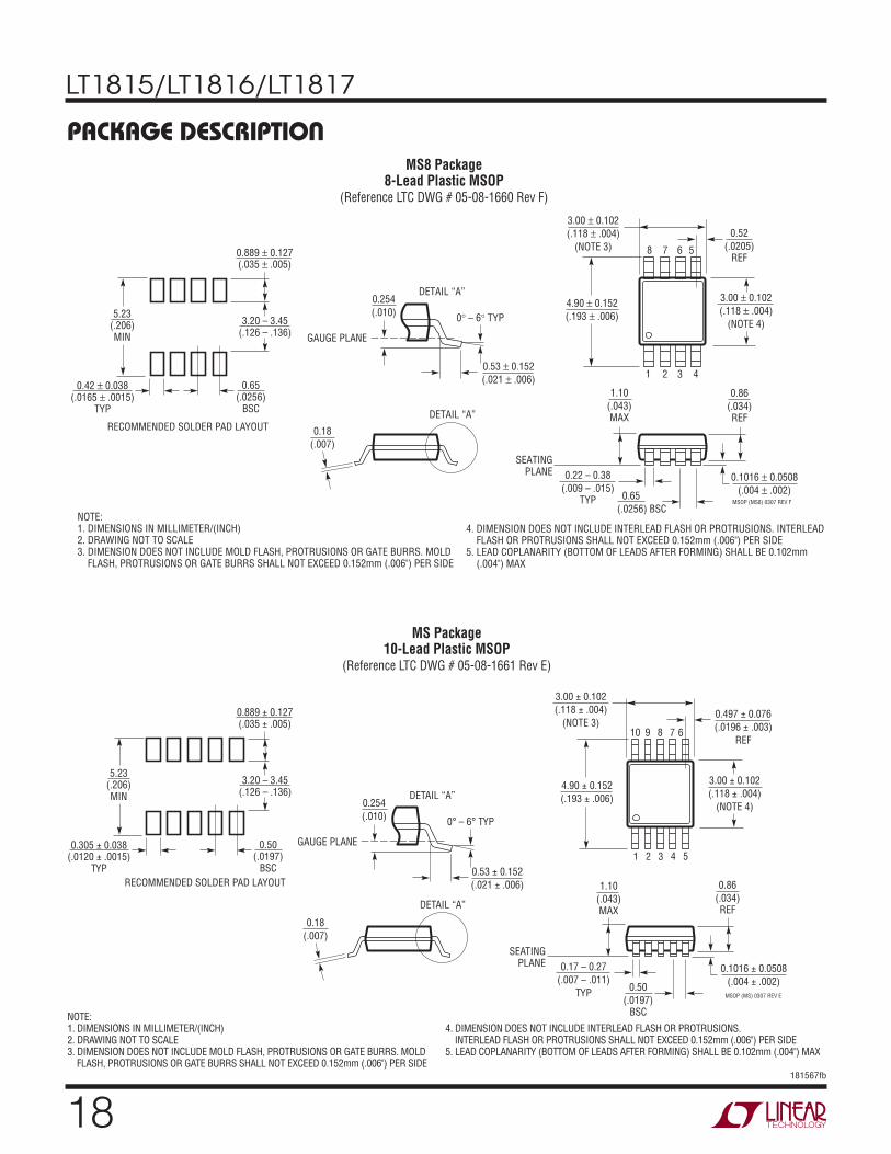
PACKAGE DESCRIPTIONMS8 Package
8-Lead Plastic MSOP(Reference LTC DWG # 05-08-1660 Rev F)
MS Package10-Lead Plastic MSOP
(Reference LTC DWG # 05-08-1661 Rev E)
MSOP (MS8) 0307 REV F
0.53 0.152(.021 .006)
SEATINGPLANE
4. DIMENSION DOES NOT INCLUDE INTERLEAD FLASH OR PROTRUSIONS. INTERLEAD FLASH OR PROTRUSIONS SHALL NOT EXCEED 0.152mm (.006") PER SIDE5. LEAD COPLANARITY (BOTTOM OF LEADS AFTER FORMING) SHALL BE 0.102mm (.004") MAX
NOTE:1. DIMENSIONS IN MILLIMETER/(INCH)2. DRAWING NOT TO SCALE3. DIMENSION DOES NOT INCLUDE MOLD FLASH, PROTRUSIONS OR GATE BURRS. MOLD FLASH, PROTRUSIONS OR GATE BURRS SHALL NOT EXCEED 0.152mm (.006") PER SIDE
0.18(.007)
0.254(.010)
1.10(.043)MAX
0.22 – 0.38(.009 – .015)
TYP
0.1016 0.0508(.004 .002)
0.86(.034)REF
0.65(.0256) BSC
0 – 6 TYP
DETAIL “A”
DETAIL “A”
GAUGE PLANE
1 2 3 4
4.90 0.152(.193 .006)
8 7 6 5
3.00 0.102(.118 .004)
(NOTE 3)
3.00 0.102(.118 .004)
(NOTE 4)
0.52(.0205)
REF
5.23(.206)MIN
3.20 – 3.45(.126 – .136)
0.889 0.127(.035 .005)
RECOMMENDED SOLDER PAD LAYOUT
0.42 0.038(.0165 .0015)
TYP
0.65(.0256)
BSC
MSOP (MS) 0307 REV E
0.53 ± 0.152(.021 ± .006)
SEATINGPLANE
0.18(.007)
1.10(.043)MAX
0.17 – 0.27(.007 – .011)
TYP
0.86(.034)REF
0.50(.0197)
BSC
1 2 3 4 5
4.90 ± 0.152(.193 ± .006)
0.497 ± 0.076(.0196 ± .003)
REF8910 7 6
3.00 ± 0.102(.118 ± .004)
(NOTE 3)
3.00 ± 0.102(.118 ± .004)
(NOTE 4)
4. DIMENSION DOES NOT INCLUDE INTERLEAD FLASH OR PROTRUSIONS. INTERLEAD FLASH OR PROTRUSIONS SHALL NOT EXCEED 0.152mm (.006") PER SIDE5. LEAD COPLANARITY (BOTTOM OF LEADS AFTER FORMING) SHALL BE 0.102mm (.004") MAX
NOTE:1. DIMENSIONS IN MILLIMETER/(INCH)2. DRAWING NOT TO SCALE3. DIMENSION DOES NOT INCLUDE MOLD FLASH, PROTRUSIONS OR GATE BURRS. MOLD FLASH, PROTRUSIONS OR GATE BURRS SHALL NOT EXCEED 0.152mm (.006") PER SIDE
0.254(.010) 0° – 6° TYP
DETAIL “A”
DETAIL “A”
GAUGE PLANE
5.23(.206)MIN
3.20 – 3.45(.126 – .136)
0.889 ± 0.127(.035 ± .005)
RECOMMENDED SOLDER PAD LAYOUT
0.305 ± 0.038(.0120 ± .0015)
TYP
0.50(.0197)
BSC
0.1016 ± 0.0508(.004 ± .002)
LT1815/LT1816/LT1817
19181567fb
Information furnished by Linear Technology Corporation is believed to be accurate and reliable. However, no responsibility is assumed for its use. Linear Technology Corporation makes no representa-tion that the interconnection of its circuits as described herein will not infringe on existing patent rights.
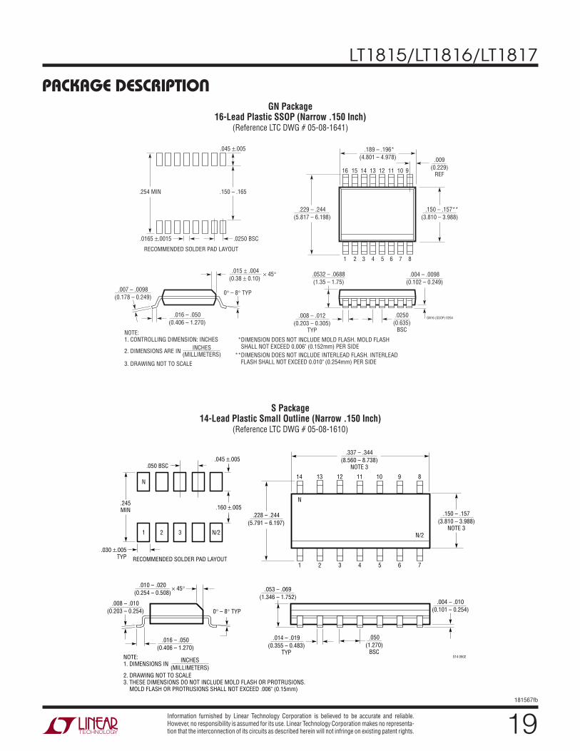
PACKAGE DESCRIPTIONGN Package
16-Lead Plastic SSOP (Narrow .150 Inch)(Reference LTC DWG # 05-08-1641)
S Package14-Lead Plastic Small Outline (Narrow .150 Inch)
(Reference LTC DWG # 05-08-1610)
1
N
2 3 4
.150 – .157(3.810 – 3.988)
NOTE 3
14 13
.337 – .344(8.560 – 8.738)
NOTE 3
.228 – .244(5.791 – 6.197)
12 11 10 9
5 6 7
N/2
8
.016 – .050(0.406 – 1.270)
.010 – .020(0.254 – 0.508)
× 45°
0° – 8° TYP.008 – .010
(0.203 – 0.254)
S14 0502
.053 – .069(1.346 – 1.752)
.014 – .019(0.355 – 0.483)
TYP
.004 – .010(0.101 – 0.254)
.050(1.270)
BSC
.245MIN
N
1 2 3 N/2
.160 ±.005
RECOMMENDED SOLDER PAD LAYOUT
.045 ±.005 .050 BSC
.030 ±.005 TYP
INCHES(MILLIMETERS)
NOTE:1. DIMENSIONS IN
2. DRAWING NOT TO SCALE3. THESE DIMENSIONS DO NOT INCLUDE MOLD FLASH OR PROTRUSIONS. MOLD FLASH OR PROTRUSIONS SHALL NOT EXCEED .006" (0.15mm)
GN16 (SSOP) 0204
1 2 3 4 5 6 7 8
.229 – .244(5.817 – 6.198)
.150 – .157**(3.810 – 3.988)
16 15 14 13
.189 – .196*(4.801 – 4.978)
12 11 10 9
.016 – .050(0.406 – 1.270)
.015 .004(0.38 0.10)
45
0 – 8 TYP.007 – .0098(0.178 – 0.249)
.0532 – .0688(1.35 – 1.75)
.008 – .012(0.203 – 0.305)
TYP
.004 – .0098(0.102 – 0.249)
.0250(0.635)
BSC
.009(0.229)
REF
.254 MIN
RECOMMENDED SOLDER PAD LAYOUT
.150 – .165
.0250 BSC.0165 .0015
.045 .005
INCHES(MILLIMETERS)
NOTE:1. CONTROLLING DIMENSION: INCHES
2. DIMENSIONS ARE IN
3. DRAWING NOT TO SCALE
* DIMENSION DOES NOT INCLUDE MOLD FLASH. MOLD FLASH SHALL NOT EXCEED 0.006" (0.152mm) PER SIDE** DIMENSION DOES NOT INCLUDE INTERLEAD FLASH. INTERLEAD FLASH SHALL NOT EXCEED 0.010" (0.254mm) PER SIDE
LT1815/LT1816/LT1817
20181567fb
Linear Technology Corporation1630 McCarthy Blvd., Milpitas, CA 95035-7417 (408) 432-1900 ● FAX: (408) 434-0507 ● www.linear.com © LINEAR TECHNOLOGY CORPORATION 2001
LT 0909 REV B • PRINTED IN USA
RELATED PARTS
TYPICAL APPLICATION
PART NUMBER DESCRIPTION COMMENTS
LT1363/LT1364/LT1365 Single/Dual/Quad 70MHz, 1V/ns, C-Load™ Op Amps Wide Supply Range: ±2.5V to ±15V
LT1395/LT1396/LT1397 Single/Dual/Quad 400MHz Current Feedback Amplifi ers 4.6mA Supply Current, 800V/μs, 80mA Output Current
LT1806/LT1807 Single/Dual 325MHz, 140V/μs Rail-to-Rail I/O Op Amps Low Noise: 3.5nV/√Hz
LT1809/LT1810 Single/Dual 180MHz, 350V/μs Rail-to-Rail I/O Op Amps Low Distortion: 90dBc at 5MHz
LT1812/LT1813/LT1814 Single/Dual/Quad 3mA, 100MHz, 750V/μs Op Amps Low Power: 3.6mA Max at ±5V
C-Load is a trademark of Linear Technology Corporation.
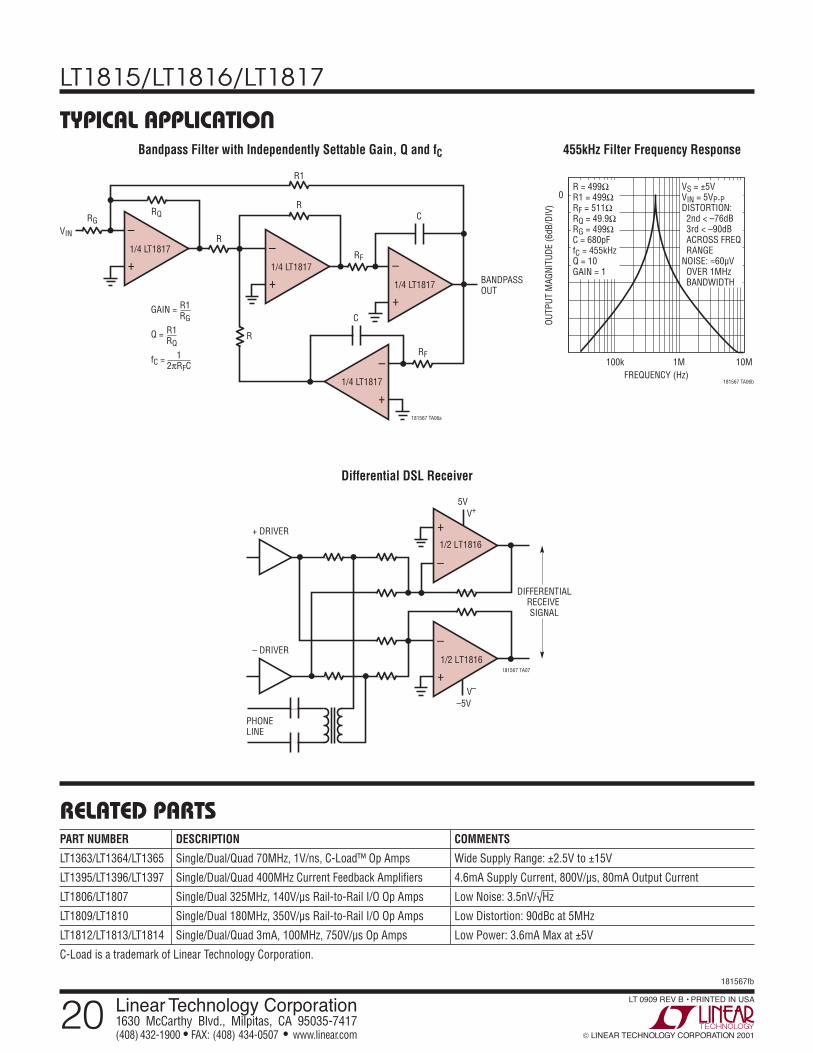
Bandpass Filter with Independently Settable Gain, Q and fC 455kHz Filter Frequency Response
Differential DSL Receiver
–
+1/4 LT1817
RGRQ
R
R1RG
RC
C
R1
RF
RF
R
VIN
GAIN =
–
+1/4 LT1817
–
+
–
+
1/4 LT1817 BANDPASSOUT
1/4 LT1817
181567 TA06a
R1RQ
Q =
12 RFC
fC =
FREQUENCY (Hz)
OUTP
UT M
AGNI
TUDE
(6dB
/DIV
)
0
100k 1M 10M
181567 TA06b
R = 499ΩR1 = 499ΩRF = 511ΩRQ = 49.9ΩRG = 499ΩC = 680pFfC = 455kHzQ = 10GAIN = 1
VS = ±5VVIN = 5VP-PDISTORTION: 2nd < –76dB 3rd < –90dB ACROSS FREQ RANGENOISE: ≈60μV OVER 1MHz BANDWIDTH
DIFFERENTIALRECEIVESIGNAL
–
+
–
+181567 TA07
PHONELINE
+ DRIVER
– DRIVER
5V
–5V
1/2 LT1816
1/2 LT1816
V+
V–