Embed Size (px)
Citation preview
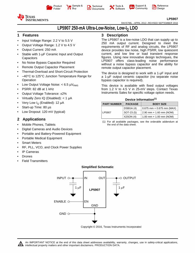
EN
IN OUT
GND
1 PF 1 PF
INPUT
ENABLE
GND
OUTPUT
LP5907
Copyright © 2016, Texas Instruments Incorporated
Product
Folder
Sample &Buy
Technical
Documents
Tools &
Software
Support &Community
ReferenceDesign
An IMPORTANT NOTICE at the end of this data sheet addresses availability, warranty, changes, use in safety-critical applications,intellectual property matters and other important disclaimers. PRODUCTION DATA.
LP5907SNVS798L –APRIL 2012–REVISED SEPTEMBER 2016
LP5907 250-mA Ultra-Low-Noise, Low-IQ LDO
1
1 Features1• Input Voltage Range: 2.2 V to 5.5 V• Output Voltage Range: 1.2 V to 4.5 V• Output Current: 250 mA• Stable with 1-µF Ceramic Input and Output
Capacitors• No Noise Bypass Capacitor Required• Remote Output Capacitor Placement• Thermal-Overload and Short-Circuit Protection• –40°C to 125°C Junction Temperature Range for
Operation• Low Output Voltage Noise: < 6.5 µVRMS
• PSRR: 82 dB at 1 kHz• Output Voltage Tolerance: ±2%• Virtually Zero IQ (Disabled): < 1 µA• Very Low IQ (Enabled): 12 µA• Start-up Time: 80 µs• Low Dropout: 120 mV (typical)
2 Applications• Mobile Phones, Tablets• Digital Cameras and Audio Devices• Portable and Battery-Powered Equipment• Portable Medical Equipment• Smart Meters• RF, PLL, VCO, and Clock Power Supplies• IP Cameras• Drones• Field Transmitters
3 DescriptionThe LP5907 is a low-noise LDO that can supply up to250 mA output current. Designed to meet therequirements of RF and analog circuits, the LP5907device provides low noise, high PSRR, low quiescentcurrent, and low line or load transient responsefigures. Using new innovative design techniques, theLP5907 offers class-leading noise performancewithout a noise bypass capacitor and the ability forremote output capacitor placement.
The device is designed to work with a 1-µF input anda 1-µF output ceramic capacitor (no separate noisebypass capacitor is required).
This device is available with fixed output voltagesfrom 1.2 V to 4.5 V in 25-mV steps. Contact TexasInstruments Sales for specific voltage option needs.
Device Information(1)
PART NUMBER PACKAGE BODY SIZE
LP5907DSBGA (4) 0.675 mm × 0.675 mm (MAX)SOT-23 (5) 2.90 mm × 1.60 mm (NOM)X2SON (4) 1.00 mm × 1.00 mm (NOM)
(1) For all available packages, see the orderable addendum atthe end of the data sheet.
space
spacespace
Simplified Schematic
2
LP5907SNVS798L –APRIL 2012–REVISED SEPTEMBER 2016 www.ti.com
Product Folder Links: LP5907
Submit Documentation Feedback Copyright © 2012–2016, Texas Instruments Incorporated
Table of Contents1 Features .................................................................. 12 Applications ........................................................... 13 Description ............................................................. 14 Revision History..................................................... 25 Pin Configuration and Functions ......................... 36 Specifications......................................................... 4
6.1 Absolute Maximum Ratings ...................................... 46.2 ESD Ratings.............................................................. 46.3 Recommended Operating Conditions....................... 46.4 Thermal Information .................................................. 56.5 Electrical Characteristics........................................... 56.6 Output and Input Capacitors ..................................... 66.7 Typical Characteristics .............................................. 7
7 Detailed Description ............................................ 117.1 Overview ................................................................. 117.2 Functional Block Diagram ....................................... 117.3 Feature Description................................................. 117.4 Device Functional Modes........................................ 12
8 Applications and Implementation ...................... 138.1 Application Information............................................ 138.2 Typical Application .................................................. 13
9 Power Supply Recommendations ...................... 1610 Layout................................................................... 17
10.1 Layout Guidelines ................................................. 1710.2 Layout Examples................................................... 1710.3 X2SON Mounting .................................................. 1810.4 DSBGA Mounting.................................................. 1810.5 DSBGA Light Sensitivity ....................................... 18
11 Device and Documentation Support ................. 1911.1 Documentation Support ........................................ 1911.2 Receiving Notification of Documentation Updates 1911.3 Community Resources.......................................... 1911.4 Trademarks ........................................................... 1911.5 Electrostatic Discharge Caution............................ 1911.6 Glossary ................................................................ 19
12 Mechanical, Packaging, and OrderableInformation ........................................................... 19
4 Revision HistoryNOTE: Page numbers for previous revisions may differ from page numbers in the current version.
Changes from Revision K (May 2016) to Revision L Page
• Changed title of data sheet and updated list of Applications ................................................................................................ 1• Changed "10 µVRMS" to "6.5 µVRMS" ....................................................................................................................................... 1• Changed wording of first sentence of Description ................................................................................................................. 1
Changes from Revision J (March 2016) to Revision K Page
• Changed "Linear Regulator" to "LDO" in title and first sentence of Description .................................................................... 1
Changes from Revision I (August 2015) to Revision J Page
• Changed VOUT min and max values and VEN min value in Abs Max table and VEN row of ROC table to correct formaterrors; replace text of footnote 2 of Abs Max table ............................................................................................................... 4
Changes from Revision H (November 2014) to Revision I Page
• Added icon for reference design to Top Navs and "ΔVOUT vs Temperature" graph to Typical Characteristics ..................... 1• Changed Storage Temperature to Abs Max table; replace Handling Ratings with ESD Ratings ......................................... 4• Deleted "VOUT ≥ 1.8 V" from first row of ΔVout spec ............................................................................................................. 5• Added "SOT-23, X2SON packages" to second row of ΔVout spec ...................................................................................... 5
Changes from Revision G (October 2013) to Revision H Page
• Added Device Information and Handling Rating tables, Feature Description, Device Functional Modes, Applicationand Implementation, Power Supply Recommendations, Layout, Device and Documentation Support, andMechanical, Packaging, and Orderable Information sections; moved some curves to Application Curves section ............. 1
N/C
1
2
3
5
4EN
GND
IN OUT
OUT
1 2
34
GND
IN EN
5
B2B1
A2A1OUT
GND
IN
ENB2 B1
A2 A1OUT
GND
IN
EN
TOP VIEW BOTTOM VIEW
3
LP5907www.ti.com SNVS798L –APRIL 2012–REVISED SEPTEMBER 2016
Product Folder Links: LP5907
Submit Documentation FeedbackCopyright © 2012–2016, Texas Instruments Incorporated
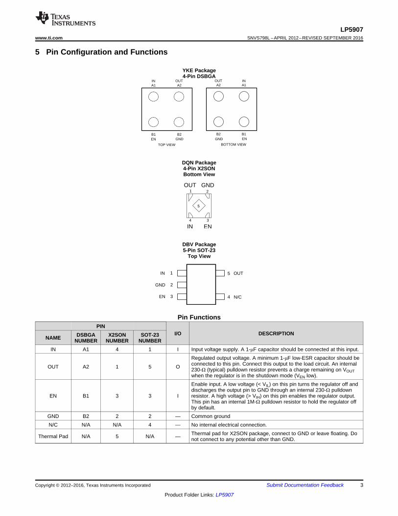
5 Pin Configuration and Functions
YKE Package4-Pin DSBGA
DQN Package4-Pin X2SONBottom View
DBV Package5-Pin SOT-23
Top View
Pin FunctionsPIN
I/O DESCRIPTIONNAME DSBGA
NUMBERX2SON
NUMBERSOT-23
NUMBERIN A1 4 1 I Input voltage supply. A 1-μF capacitor should be connected at this input.
OUT A2 1 5 O
Regulated output voltage. A minimum 1-μF low-ESR capacitor should beconnected to this pin. Connect this output to the load circuit. An internal230-Ω (typical) pulldown resistor prevents a charge remaining on VOUTwhen the regulator is in the shutdown mode (VEN low).
EN B1 3 3 I
Enable input. A low voltage (< VIL) on this pin turns the regulator off anddischarges the output pin to GND through an internal 230-Ω pulldownresistor. A high voltage (> VIH) on this pin enables the regulator output.This pin has an internal 1M-Ω pulldown resistor to hold the regulator offby default.
GND B2 2 2 — Common groundN/C N/A N/A 4 — No internal electrical connection.
Thermal Pad N/A 5 N/A — Thermal pad for X2SON package, connect to GND or leave floating. Donot connect to any potential other than GND.
4
LP5907SNVS798L –APRIL 2012–REVISED SEPTEMBER 2016 www.ti.com
Product Folder Links: LP5907
Submit Documentation Feedback Copyright © 2012–2016, Texas Instruments Incorporated
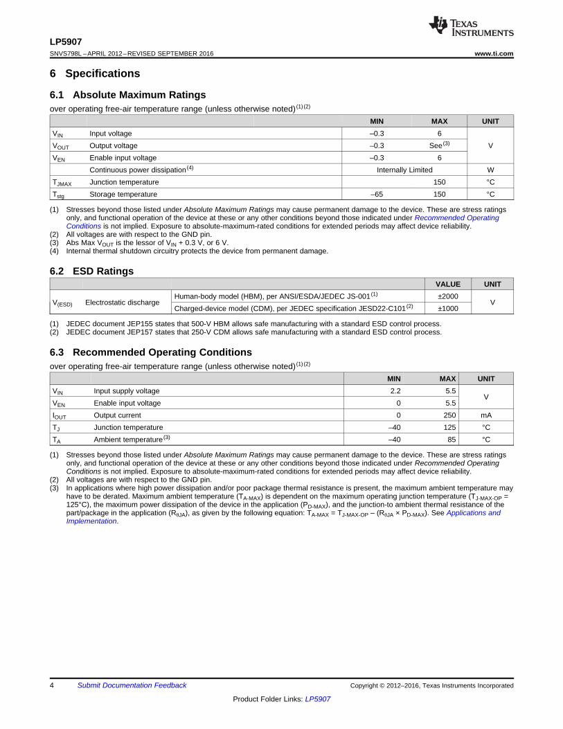
(1) Stresses beyond those listed under Absolute Maximum Ratings may cause permanent damage to the device. These are stress ratingsonly, and functional operation of the device at these or any other conditions beyond those indicated under Recommended OperatingConditions is not implied. Exposure to absolute-maximum-rated conditions for extended periods may affect device reliability.
(2) All voltages are with respect to the GND pin.(3) Abs Max VOUT is the lessor of VIN + 0.3 V, or 6 V.(4) Internal thermal shutdown circuitry protects the device from permanent damage.
6 Specifications
6.1 Absolute Maximum Ratingsover operating free-air temperature range (unless otherwise noted) (1) (2)
MIN MAX UNITVIN Input voltage –0.3 6
VVOUT Output voltage –0.3 See (3)
VEN Enable input voltage –0.3 6Continuous power dissipation (4) Internally Limited W
TJMAX Junction temperature 150 °CTstg Storage temperature –65 150 °C
(1) JEDEC document JEP155 states that 500-V HBM allows safe manufacturing with a standard ESD control process.(2) JEDEC document JEP157 states that 250-V CDM allows safe manufacturing with a standard ESD control process.
6.2 ESD RatingsVALUE UNIT
V(ESD) Electrostatic dischargeHuman-body model (HBM), per ANSI/ESDA/JEDEC JS-001 (1) ±2000
VCharged-device model (CDM), per JEDEC specification JESD22-C101 (2) ±1000
(1) Stresses beyond those listed under Absolute Maximum Ratings may cause permanent damage to the device. These are stress ratingsonly, and functional operation of the device at these or any other conditions beyond those indicated under Recommended OperatingConditions is not implied. Exposure to absolute-maximum-rated conditions for extended periods may affect device reliability.
(2) All voltages are with respect to the GND pin.(3) In applications where high power dissipation and/or poor package thermal resistance is present, the maximum ambient temperature may
have to be derated. Maximum ambient temperature (TA-MAX) is dependent on the maximum operating junction temperature (TJ-MAX-OP =125°C), the maximum power dissipation of the device in the application (PD-MAX), and the junction-to ambient thermal resistance of thepart/package in the application (RθJA), as given by the following equation: TA-MAX = TJ-MAX-OP – (RθJA × PD-MAX). See Applications andImplementation.
6.3 Recommended Operating Conditionsover operating free-air temperature range (unless otherwise noted) (1) (2)
MIN MAX UNITVIN Input supply voltage 2.2 5.5
VVEN Enable input voltage 0 5.5IOUT Output current 0 250 mATJ Junction temperature –40 125 °CTA Ambient temperature (3) –40 85 °C
5
LP5907www.ti.com SNVS798L –APRIL 2012–REVISED SEPTEMBER 2016
Product Folder Links: LP5907
Submit Documentation FeedbackCopyright © 2012–2016, Texas Instruments Incorporated
(1) For more information about traditional and new thermal metrics, see the Semiconductor and IC Package Thermal Metrics applicationreport, SPRA953.
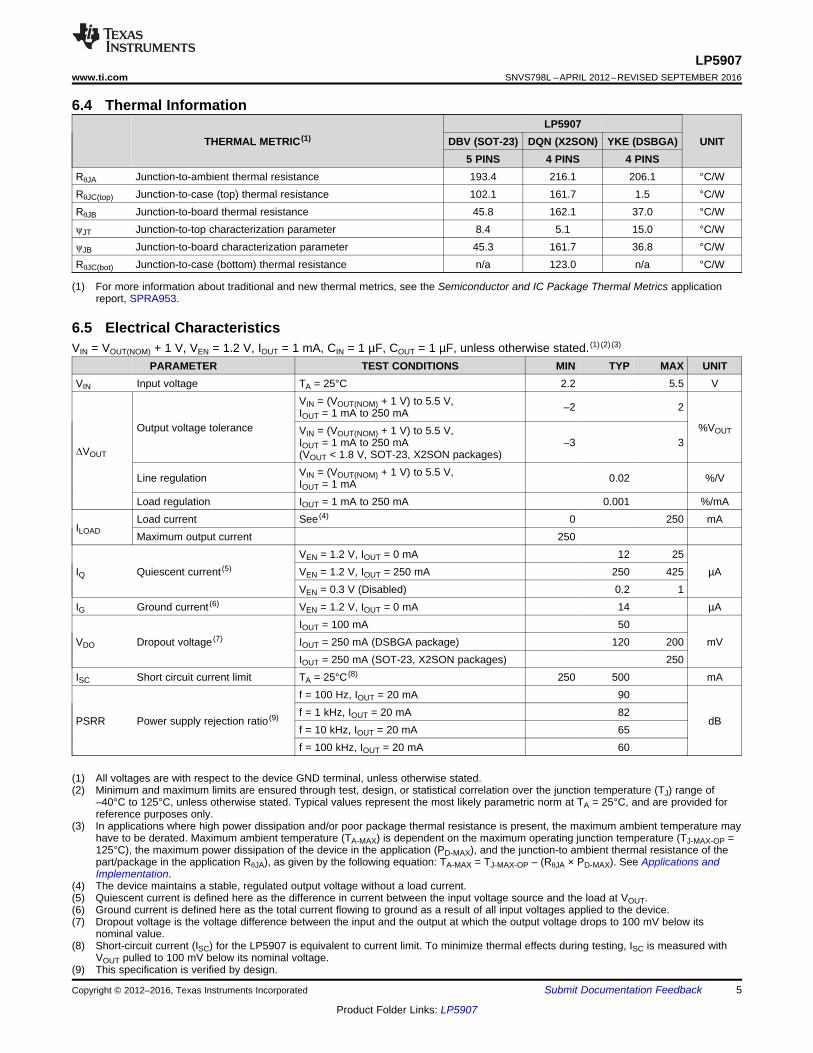
6.4 Thermal Information
THERMAL METRIC (1)LP5907
UNITDBV (SOT-23) DQN (X2SON) YKE (DSBGA)5 PINS 4 PINS 4 PINS
RθJA Junction-to-ambient thermal resistance 193.4 216.1 206.1 °C/WRθJC(top) Junction-to-case (top) thermal resistance 102.1 161.7 1.5 °C/WRθJB Junction-to-board thermal resistance 45.8 162.1 37.0 °C/WψJT Junction-to-top characterization parameter 8.4 5.1 15.0 °C/WψJB Junction-to-board characterization parameter 45.3 161.7 36.8 °C/WRθJC(bot) Junction-to-case (bottom) thermal resistance n/a 123.0 n/a °C/W
(1) All voltages are with respect to the device GND terminal, unless otherwise stated.(2) Minimum and maximum limits are ensured through test, design, or statistical correlation over the junction temperature (TJ) range of
–40°C to 125°C, unless otherwise stated. Typical values represent the most likely parametric norm at TA = 25°C, and are provided forreference purposes only.
(3) In applications where high power dissipation and/or poor package thermal resistance is present, the maximum ambient temperature mayhave to be derated. Maximum ambient temperature (TA-MAX) is dependent on the maximum operating junction temperature (TJ-MAX-OP =125°C), the maximum power dissipation of the device in the application (PD-MAX), and the junction-to ambient thermal resistance of thepart/package in the application RθJA), as given by the following equation: TA-MAX = TJ-MAX-OP – (RθJA × PD-MAX). See Applications andImplementation.
(4) The device maintains a stable, regulated output voltage without a load current.(5) Quiescent current is defined here as the difference in current between the input voltage source and the load at VOUT.(6) Ground current is defined here as the total current flowing to ground as a result of all input voltages applied to the device.(7) Dropout voltage is the voltage difference between the input and the output at which the output voltage drops to 100 mV below its
nominal value.(8) Short-circuit current (ISC) for the LP5907 is equivalent to current limit. To minimize thermal effects during testing, ISC is measured with
VOUT pulled to 100 mV below its nominal voltage.(9) This specification is verified by design.
6.5 Electrical CharacteristicsVIN = VOUT(NOM) + 1 V, VEN = 1.2 V, IOUT = 1 mA, CIN = 1 µF, COUT = 1 µF, unless otherwise stated. (1) (2) (3)
PARAMETER TEST CONDITIONS MIN TYP MAX UNITVIN Input voltage TA = 25°C 2.2 5.5 V
ΔVOUT
Output voltage tolerance
VIN = (VOUT(NOM) + 1 V) to 5.5 V,IOUT = 1 mA to 250 mA –2 2
%VOUTVIN = (VOUT(NOM) + 1 V) to 5.5 V,IOUT = 1 mA to 250 mA(VOUT < 1.8 V, SOT-23, X2SON packages)
–3 3
Line regulation VIN = (VOUT(NOM) + 1 V) to 5.5 V,IOUT = 1 mA 0.02 %/V
Load regulation IOUT = 1 mA to 250 mA 0.001 %/mA
ILOADLoad current See (4) 0 250 mAMaximum output current 250
IQ Quiescent current (5)
VEN = 1.2 V, IOUT = 0 mA 12 25µAVEN = 1.2 V, IOUT = 250 mA 250 425
VEN = 0.3 V (Disabled) 0.2 1IG Ground current (6) VEN = 1.2 V, IOUT = 0 mA 14 µA
VDO Dropout voltage (7)
IOUT = 100 mA 50mVIOUT = 250 mA (DSBGA package) 120 200
IOUT = 250 mA (SOT-23, X2SON packages) 250ISC Short circuit current limit TA = 25°C (8) 250 500 mA
PSRR Power supply rejection ratio (9)
f = 100 Hz, IOUT = 20 mA 90
dBf = 1 kHz, IOUT = 20 mA 82f = 10 kHz, IOUT = 20 mA 65f = 100 kHz, IOUT = 20 mA 60
6
LP5907SNVS798L –APRIL 2012–REVISED SEPTEMBER 2016 www.ti.com
Product Folder Links: LP5907
Submit Documentation Feedback Copyright © 2012–2016, Texas Instruments Incorporated
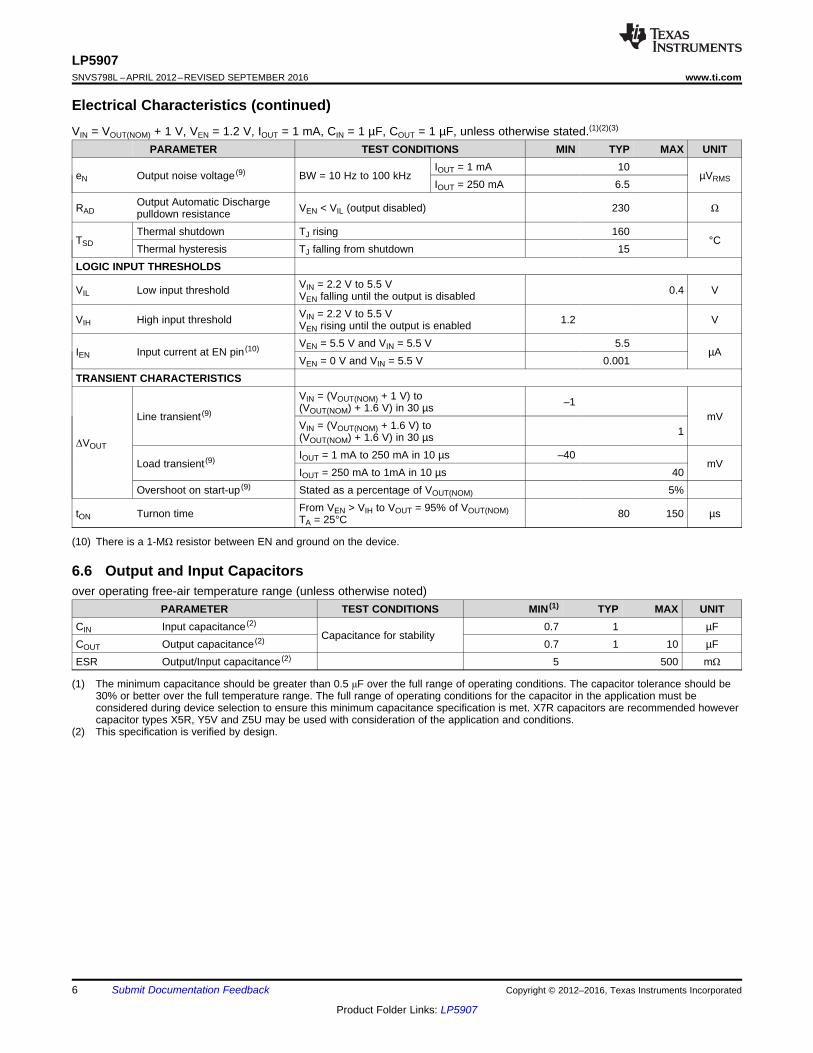
Electrical Characteristics (continued)VIN = VOUT(NOM) + 1 V, VEN = 1.2 V, IOUT = 1 mA, CIN = 1 µF, COUT = 1 µF, unless otherwise stated.(1)(2)(3)
PARAMETER TEST CONDITIONS MIN TYP MAX UNIT
(10) There is a 1-MΩ resistor between EN and ground on the device.
eN Output noise voltage (9) BW = 10 Hz to 100 kHzIOUT = 1 mA 10
µVRMSIOUT = 250 mA 6.5
RADOutput Automatic Dischargepulldown resistance VEN < VIL (output disabled) 230 Ω
TSDThermal shutdown TJ rising 160
°CThermal hysteresis TJ falling from shutdown 15
LOGIC INPUT THRESHOLDS
VIL Low input threshold VIN = 2.2 V to 5.5 VVEN falling until the output is disabled 0.4 V
VIH High input threshold VIN = 2.2 V to 5.5 VVEN rising until the output is enabled 1.2 V
IEN Input current at EN pin (10) VEN = 5.5 V and VIN = 5.5 V 5.5µA
VEN = 0 V and VIN = 5.5 V 0.001TRANSIENT CHARACTERISTICS
ΔVOUT
Line transient (9)
VIN = (VOUT(NOM) + 1 V) to(VOUT(NOM) + 1.6 V) in 30 µs –1
mVVIN = (VOUT(NOM) + 1.6 V) to(VOUT(NOM) + 1.6 V) in 30 µs 1
Load transient (9) IOUT = 1 mA to 250 mA in 10 µs –40mV
IOUT = 250 mA to 1mA in 10 µs 40Overshoot on start-up (9) Stated as a percentage of VOUT(NOM) 5%
tON Turnon time From VEN > VIH to VOUT = 95% of VOUT(NOM)TA = 25°C 80 150 µs
(1) The minimum capacitance should be greater than 0.5 μF over the full range of operating conditions. The capacitor tolerance should be30% or better over the full temperature range. The full range of operating conditions for the capacitor in the application must beconsidered during device selection to ensure this minimum capacitance specification is met. X7R capacitors are recommended howevercapacitor types X5R, Y5V and Z5U may be used with consideration of the application and conditions.
(2) This specification is verified by design.
6.6 Output and Input Capacitorsover operating free-air temperature range (unless otherwise noted)
PARAMETER TEST CONDITIONS MIN (1) TYP MAX UNITCIN Input capacitance (2)
Capacitance for stability0.7 1 µF
COUT Output capacitance (2) 0.7 1 10 µFESR Output/Input capacitance (2) 5 500 mΩ
0 50 100 150 200 250 300
0
50
100
150
200
250
300
350
GR
OU
ND
CU
RR
EN
T (�
A)
IOUT(mA)
VIN = 3.0VVIN = 3.8VVIN = 4.2VVIN = 5.5V
SVA-30180571
0 50 100 150 200 250
2.700
2.725
2.750
2.775
2.800
2.825
2.850
2.875
2.900
VO
UT
(V)
LOAD (mA)
VIN= 3.6V
-40°C90°C25°C
SVA-30180567
VIN (V)
VO
UT
(V
)
0 0.5 1 1.5 2 2.50
0.2
0.4
0.6
0.8
1
1.2
1.4
D002
RLOAD = 1.2 k:RLOAD = 4.8 :
VIN (V)
VO
UT
(V
)
0 1 2 3 4 5 60
0.5
1
1.5
2
2.5
3
3.5
4
4.5
5
D003
RLOAD = 4.5 k:RLOAD = 18 :
2.3 2.8 3.3 3.8 4.3 4.8 5.3 5.8
0
2
4
6
8
10
12
14
16
I Q(�
A)
VIN(V)SVA-30180569
VIN (V)
VE
N (
V)
2 2.5 3 3.5 4 4.5 5 5.5 60.5
0.6
0.7
0.8
0.9
1
D001
VIH RisingVIL Falling
7
LP5907www.ti.com SNVS798L –APRIL 2012–REVISED SEPTEMBER 2016
Product Folder Links: LP5907
Submit Documentation FeedbackCopyright © 2012–2016, Texas Instruments Incorporated
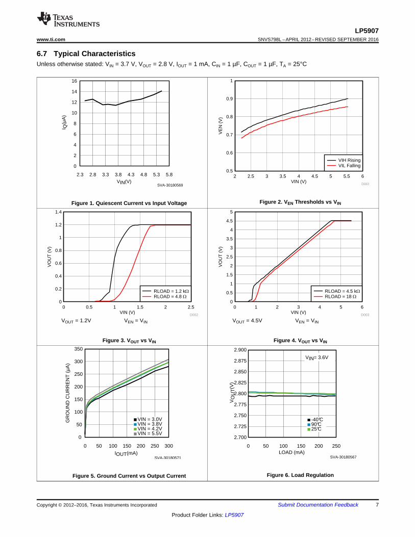
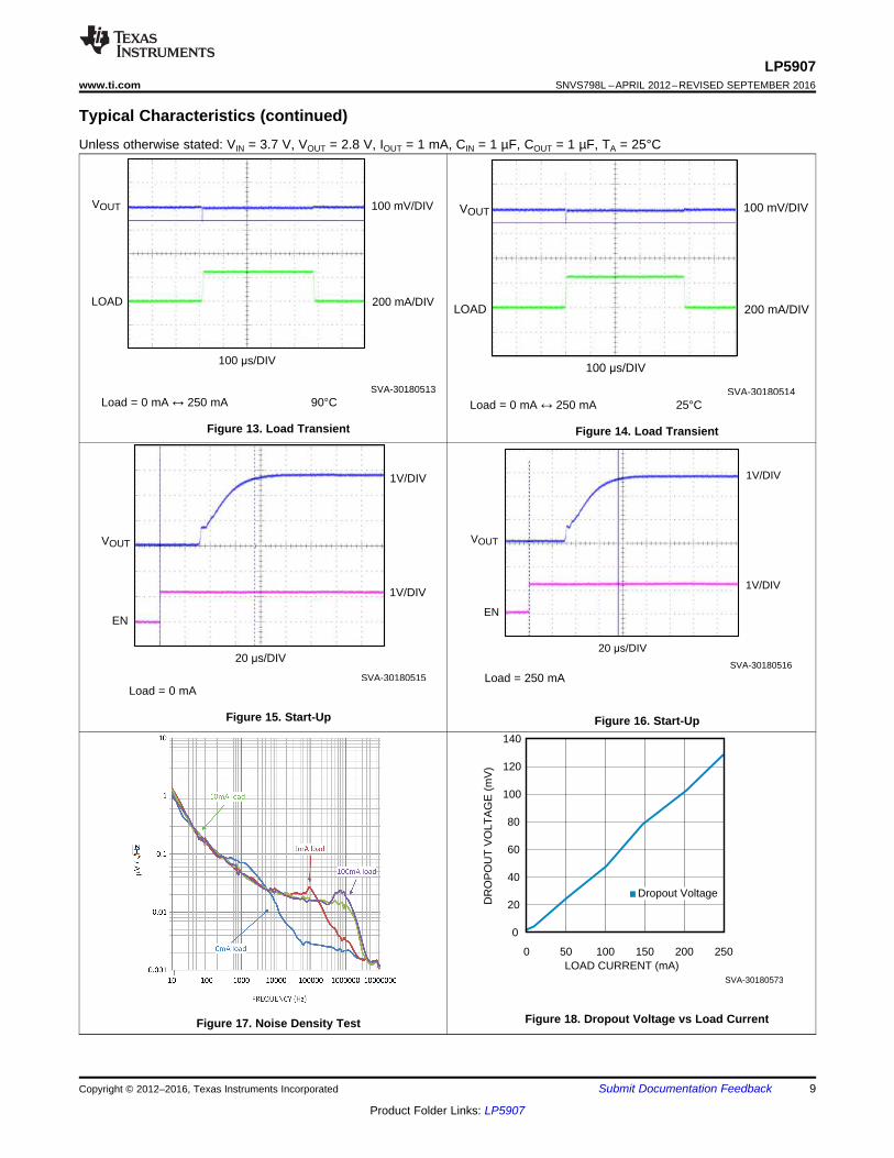
6.7 Typical CharacteristicsUnless otherwise stated: VIN = 3.7 V, VOUT = 2.8 V, IOUT = 1 mA, CIN = 1 µF, COUT = 1 µF, TA = 25°C
Figure 1. Quiescent Current vs Input Voltage Figure 2. VEN Thresholds vs VIN
VOUT = 1.2V VEN = VIN
Figure 3. VOUT vs VIN
VOUT = 4.5V VEN = VIN
Figure 4. VOUT vs VIN
Figure 5. Ground Current vs Output Current Figure 6. Load Regulation
100 �s/DIV
VOUT 100 mV/DIV
LOAD 200 mA/DIV
SVA-30180512
10 �s/DIV
10 mV/DIV
1V/DIVVIN
VOUT (AC Coupled)
SVA-30180511
10 �s/DIV
VOUT (AC Coupled)
10 mV/DIV
1V/DIVVIN
SVA-30180510
2 ms/DIV
VOUT
2V/DIV
2V/DIV
1A/DIV
VIN = VEN
IIN
SVA-30180509
Junction Temperature (qC)
'V
OU
T (
%)
-50 -25 0 25 50 75 100 125-0.4
-0.3
-0.2
-0.1
0
0.1
0.2
D010
3.0 3.5 4.0 4.5 5.0 5.5
2.700
2.725
2.750
2.775
2.800
2.825
2.850
2.875
2.900
VO
UT
(V)
VIN(V)
Load = 10 mA
-40°C90°C25°C
SVA-30180568
8
LP5907SNVS798L –APRIL 2012–REVISED SEPTEMBER 2016 www.ti.com
Product Folder Links: LP5907
Submit Documentation Feedback Copyright © 2012–2016, Texas Instruments Incorporated
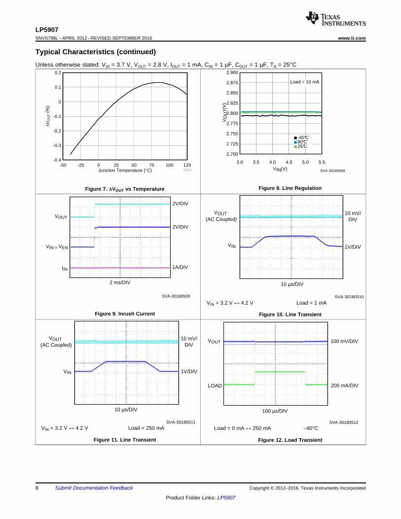
Typical Characteristics (continued)Unless otherwise stated: VIN = 3.7 V, VOUT = 2.8 V, IOUT = 1 mA, CIN = 1 µF, COUT = 1 µF, TA = 25°C
Figure 7. ΔVOUT vs Temperature Figure 8. Line Regulation
Figure 9. Inrush Current
VIN = 3.2 V ↔ 4.2 V Load = 1 mA
Figure 10. Line Transient
VIN = 3.2 V ↔ 4.2 V Load = 250 mA
Figure 11. Line Transient
Load = 0 mA ↔ 250 mA –40°C
Figure 12. Load Transient
0 50 100 150 200 250
0
20
40
60
80
100
120
140
DR
OP
OU
T V
OLT
AG
E (
mV
)
LOAD CURRENT (mA)
Dropout Voltage
SVA-30180573
20 �s/DIV
VOUT
1V/DIV
EN
1V/DIV
SVA-30180515
20 �s/DIV
VOUT
1V/DIV
EN
1V/DIV
SVA-30180516
100 �s/DIV
VOUT 100 mV/DIV
LOAD 200 mA/DIV
SVA-30180514
100 �s/DIV
VOUT 100 mV/DIV
LOAD 200 mA/DIV
SVA-30180513
9
LP5907www.ti.com SNVS798L –APRIL 2012–REVISED SEPTEMBER 2016
Product Folder Links: LP5907
Submit Documentation FeedbackCopyright © 2012–2016, Texas Instruments Incorporated
Typical Characteristics (continued)Unless otherwise stated: VIN = 3.7 V, VOUT = 2.8 V, IOUT = 1 mA, CIN = 1 µF, COUT = 1 µF, TA = 25°C
Load = 0 mA ↔ 250 mA 90°C
Figure 13. Load Transient
Load = 0 mA ↔ 250 mA 25°C
Figure 14. Load Transient
Load = 0 mA
Figure 15. Start-Up
Load = 250 mA
Figure 16. Start-Up
Figure 17. Noise Density Test Figure 18. Dropout Voltage vs Load Current
FREQUENCY (kHz)
PS
RR
(dB
)
0.1 1 10 100-120
-100
-80
-60
-40
-20
0
D004
250 mA200 mA150 mA100 mA50 mA20 mA
FREQUENCY (kHz)
PS
RR
(dB
)
0.01 0.1 1 10 100 1000 10000-120
-100
-80
-60
-40
-20
0
D005
250 mA200 mA150 mA100 mA50 mA20 mA
10
LP5907SNVS798L –APRIL 2012–REVISED SEPTEMBER 2016 www.ti.com
Product Folder Links: LP5907
Submit Documentation Feedback Copyright © 2012–2016, Texas Instruments Incorporated
Typical Characteristics (continued)Unless otherwise stated: VIN = 3.7 V, VOUT = 2.8 V, IOUT = 1 mA, CIN = 1 µF, COUT = 1 µF, TA = 25°C
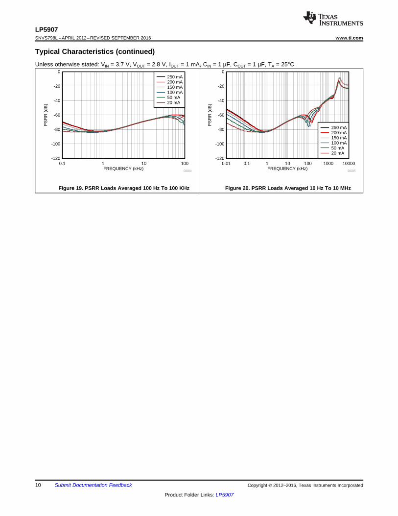
Figure 19. PSRR Loads Averaged 100 Hz To 100 KHz Figure 20. PSRR Loads Averaged 10 Hz To 10 MHz
IN
VBG1.20V
EN
+ ENEN
GND
POR
+
OUT
1 M VIH
RFCF
+
EN
EN
RAD
Copyright © 2016, Texas Instruments Incorporated
11
LP5907www.ti.com SNVS798L –APRIL 2012–REVISED SEPTEMBER 2016
Product Folder Links: LP5907
Submit Documentation FeedbackCopyright © 2012–2016, Texas Instruments Incorporated
7 Detailed Description
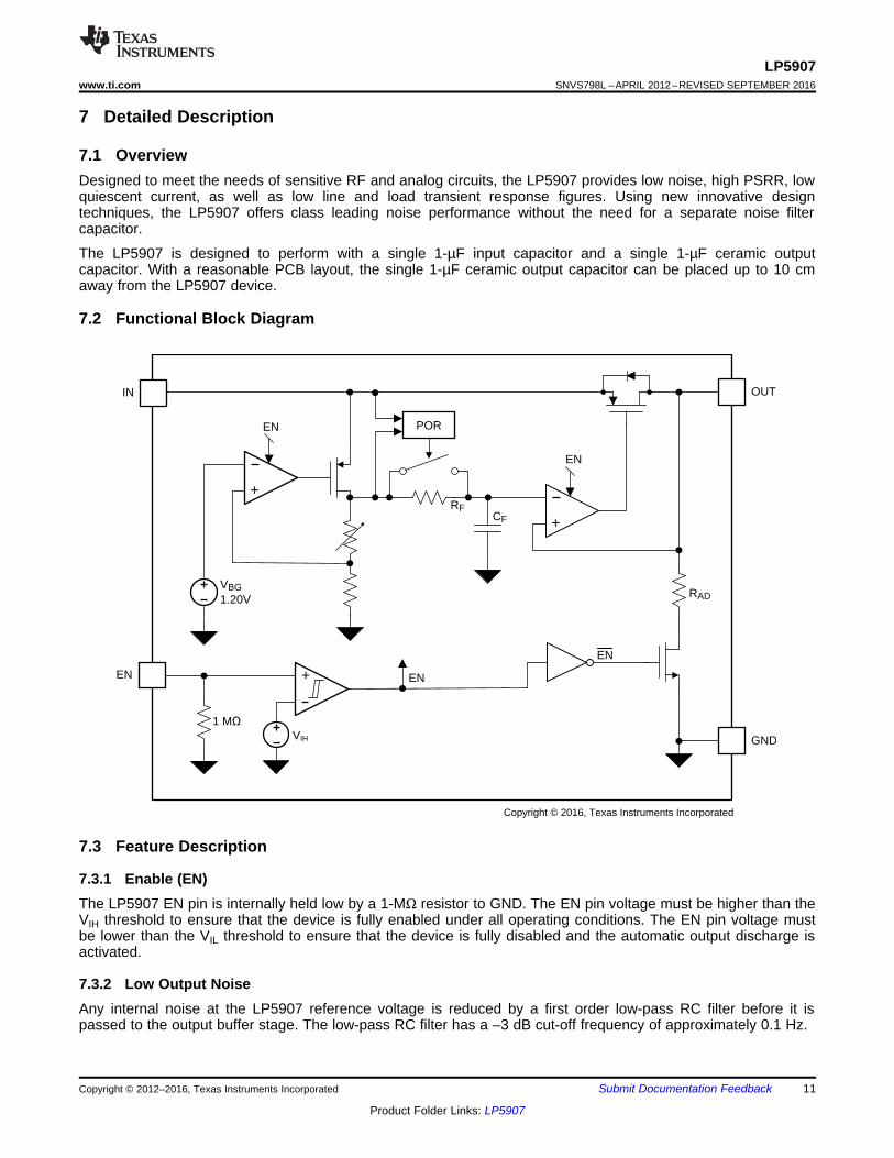
7.1 OverviewDesigned to meet the needs of sensitive RF and analog circuits, the LP5907 provides low noise, high PSRR, lowquiescent current, as well as low line and load transient response figures. Using new innovative designtechniques, the LP5907 offers class leading noise performance without the need for a separate noise filtercapacitor.
The LP5907 is designed to perform with a single 1-µF input capacitor and a single 1-µF ceramic outputcapacitor. With a reasonable PCB layout, the single 1-µF ceramic output capacitor can be placed up to 10 cmaway from the LP5907 device.
7.2 Functional Block Diagram
7.3 Feature Description
7.3.1 Enable (EN)The LP5907 EN pin is internally held low by a 1-MΩ resistor to GND. The EN pin voltage must be higher than theVIH threshold to ensure that the device is fully enabled under all operating conditions. The EN pin voltage mustbe lower than the VIL threshold to ensure that the device is fully disabled and the automatic output discharge isactivated.
7.3.2 Low Output NoiseAny internal noise at the LP5907 reference voltage is reduced by a first order low-pass RC filter before it ispassed to the output buffer stage. The low-pass RC filter has a –3 dB cut-off frequency of approximately 0.1 Hz.
12
LP5907SNVS798L –APRIL 2012–REVISED SEPTEMBER 2016 www.ti.com
Product Folder Links: LP5907
Submit Documentation Feedback Copyright © 2012–2016, Texas Instruments Incorporated
Feature Description (continued)7.3.3 Output Automatic DischargeThe LP5907 output employs an internal 230-Ω (typical) pulldown resistance to discharge the output when the ENpin is low, and the device is disabled.
7.3.4 Remote Output Capacitor PlacementThe LP5907 requires at least a 1-µF capacitor at the OUT pin, but there are no strict requirements about thelocation of the capacitor in regards the OUT pin. In practical designs, the output capacitor may be located up to10 cm away from the LDO.
7.3.5 Thermal Overload Protection (TSD)Thermal shutdown disables the output when the junction temperature rises to approximately 160°C which allowsthe device to cool. When the junction temperature cools to approximately 145°C, the output circuitry enables.Based on power dissipation, thermal resistance, and ambient temperature, the thermal protection circuit maycycle on and off. This thermal cycling limits the dissipation of the regulator and protects it from damage as aresult of overheating.
The thermal shutdown circuitry of the LP5907 has been designed to protect against temporary thermal overloadconditions. The TSD circuitry was not intended to replace proper heat-sinking. Continuously running the LP5907device into thermal shutdown may degrade device reliability.
7.4 Device Functional Modes
7.4.1 Enable (EN)The LP5907 Enable (EN) pin is internally held low by a 1-MΩ resistor to GND. The EN pin voltage must behigher than the VIH threshold to ensure that the device is fully enabled under all operating conditions.
When the EN pin is pulled low, and the output is disabled, the output automatic discharge circuitry is activated.Any charge on the OUT pin is discharged to GND through the internal 230-Ω (typical) pulldown resistance.
7.4.2 Minimum Operating Input Voltage (VIN)The LP5907 does not include any dedicated UVLO circuitry. The LP5907 internal circuitry is not fully functionaluntil VIN is at least 2.2 V. The output voltage is not regulated until VIN has reached at least the greater of 2.2 V or(VOUT + VDO).
EN
IN OUT
GND
1 PF 1 PF
INPUT
ENABLE
GND
OUTPUT
LP5907
Copyright © 2016, Texas Instruments Incorporated
13
LP5907www.ti.com SNVS798L –APRIL 2012–REVISED SEPTEMBER 2016
Product Folder Links: LP5907
Submit Documentation FeedbackCopyright © 2012–2016, Texas Instruments Incorporated
8 Applications and Implementation
NOTEInformation in the following applications sections is not part of the TI componentspecification, and TI does not warrant its accuracy or completeness. TI’s customers areresponsible for determining suitability of components for their purposes. Customers shouldvalidate and test their design implementation to confirm system functionality.
8.1 Application InformationThe LP5907 is designed to meet the requirements of RF and analog circuits, by providing low noise, high PSRR,low quiescent current, and low line or load transient response figures. The device offers excellent noiseperformance without the need for a noise bypass capacitor and is stable with input and output capacitors with avalue of 1 µF. The LP5907 delivers this performance in industry standard packages such as DSBGA, X2SON,and SOT-23 which, for this device, are specified with an operating junction temperature (TJ) of –40°C to 125°C.
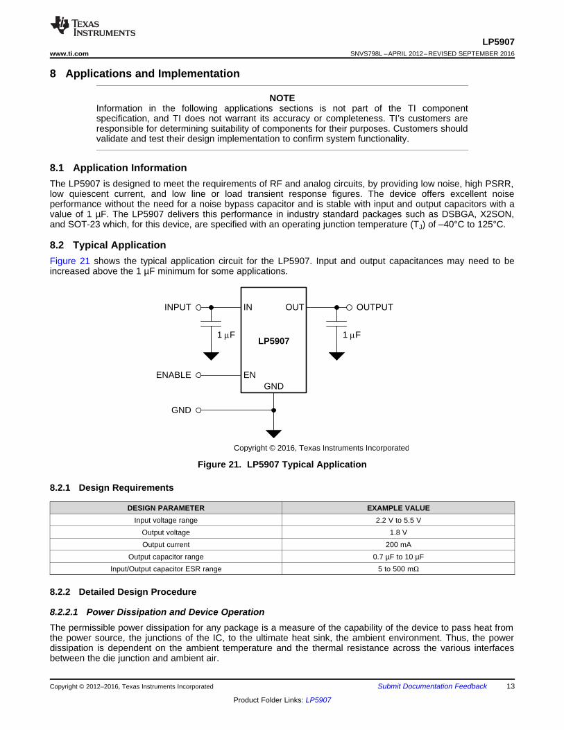
8.2 Typical ApplicationFigure 21 shows the typical application circuit for the LP5907. Input and output capacitances may need to beincreased above the 1 µF minimum for some applications.
Figure 21. LP5907 Typical Application
8.2.1 Design Requirements
DESIGN PARAMETER EXAMPLE VALUEInput voltage range 2.2 V to 5.5 V
Output voltage 1.8 VOutput current 200 mA
Output capacitor range 0.7 µF to 10 µFInput/Output capacitor ESR range 5 to 500 mΩ
8.2.2 Detailed Design Procedure
8.2.2.1 Power Dissipation and Device OperationThe permissible power dissipation for any package is a measure of the capability of the device to pass heat fromthe power source, the junctions of the IC, to the ultimate heat sink, the ambient environment. Thus, the powerdissipation is dependent on the ambient temperature and the thermal resistance across the various interfacesbetween the die junction and ambient air.
14
LP5907SNVS798L –APRIL 2012–REVISED SEPTEMBER 2016 www.ti.com
Product Folder Links: LP5907
Submit Documentation Feedback Copyright © 2012–2016, Texas Instruments Incorporated
The maximum allowable power dissipation for the device in a given package can be calculated using Equation 1:PD-MAX = ((TJ-MAX – TA) / RθJA) (1)
The actual power being dissipated in the device can be represented by Equation 2:PD = (VIN – VOUT) × IOUT (2)
These two equations establish the relationship between the maximum power dissipation allowed due to thermalconsideration, the voltage drop across the device, and the continuous current capability of the device. These twoequations should be used to determine the optimum operating conditions for the device in the application.
In applications where lower power dissipation (PD) and/or excellent package thermal resistance (RθJA) is present,the maximum ambient temperature (TA-MAX) may be increased.
In applications where high power dissipation and/or poor package thermal resistance is present, the maximumambient temperature (TA-MAX) may have to be derated. TA-MAX is dependent on the maximum operating junctiontemperature (TJ-MAX-OP = 125°C), the maximum allowable power dissipation in the device package in theapplication (PD-MAX), and the junction-to ambient thermal resistance of the part/package in the application (RθJA),as given by Equation 3:
TA-MAX = (TJ-MAX-OP – (RθJA × PD-MAX)) (3)
Alternately, if TA-MAX can not be derated, the PD value must be reduced. This can be accomplished by reducingVIN in the VIN–VOUT term as long as the minimum VIN is met, or by reducing the IOUT term, or by somecombination of the two.
8.2.2.2 External CapacitorsLike most low-dropout regulators, the LP5907 requires external capacitors for regulator stability. The device isspecifically designed for portable applications requiring minimum board space and smallest components. Thesecapacitors must be correctly selected for good performance.
8.2.2.3 Input CapacitorAn input capacitor is required for stability. The input capacitor should be at least equal to, or greater than, theoutput capacitor for good load transient performance. At least a 1 µF capacitor has to be connected between theLP5907 input pin and ground for stable operation over full load current range. Basically, it is ok to have moreoutput capacitance than input, as long as the input is at least 1 µF.
The input capacitor must be located a distance of not more than 1 cm from the input pin and returned to a cleananalog ground. Any good quality ceramic, tantalum, or film capacitor may be used at the input.
NOTETo ensure stable operation it is essential that good PCB practices are employed tominimize ground impedance and keep input inductance low. If these conditions cannot bemet, or if long leads are to be used to connect the battery or other power source to theLP5907, TI recommends increasing the input capacitor to at least 10 µF. Also, tantalumcapacitors can suffer catastrophic failures due to surge current when connected to a low-impedance source of power (like a battery or a very large capacitor). If a tantalumcapacitor is used at the input, it should be verified by the manufacturer to have a surgecurrent rating sufficient for the application. The initial tolerance, applied voltage de-rating,and temperature coefficient must all be considered when selecting the input capacitor toensure the actual capacitance is never less than 0.7 µF over the entire operating range.
8.2.2.4 Output CapacitorThe LP5907 is designed specifically to work with a very small ceramic output capacitor, typically 1 µF. A ceramiccapacitor (dielectric types X5R or X7R) in the 1 µF to 10 µF range, and with ESR between 5 mΩ to 500 mΩ, issuitable in the LP5907 application circuit. For this device the output capacitor should be connected between theOUT pin and a good connection back to the GND pin.
It may also be possible to use tantalum or film capacitors at the device output, VOUT, but these are not asattractive for reasons of size and cost (see Capacitor Characteristics).
15
LP5907www.ti.com SNVS798L –APRIL 2012–REVISED SEPTEMBER 2016
Product Folder Links: LP5907
Submit Documentation FeedbackCopyright © 2012–2016, Texas Instruments Incorporated
The output capacitor must meet the requirement for the minimum value of capacitance and have an ESR valuethat is within the range 5 mΩ to 500 mΩ for stability. Like the input capacitor, the initial tolerance, applied voltagede-rating, and temperature coefficient must all be considered when selecting the input capacitor to ensure theactual capacitance is never less than 0.7 µF over the entire operating range.
8.2.2.5 Capacitor CharacteristicsThe LP5907 is designed to work with ceramic capacitors on the input and output to take advantage of thebenefits they offer. For capacitance values in the range of 1 µF to 10 µF, ceramic capacitors are the smallest,least expensive and have the lowest ESR values, thus making them best for eliminating high frequency noise.The ESR of a typical 1 µF ceramic capacitor is in the range of 20 mΩ to 40 mΩ, which easily meets the ESRrequirement for stability for the LP5907.
A better choice for temperature coefficient in a ceramic capacitor is X7R. This type of capacitor is the most stableand holds the capacitance within ±15% over the temperature range. Tantalum capacitors are less desirable thanceramic for use as output capacitors because they are more expensive when comparing equivalent capacitanceand voltage ratings in the 1 µF to 10 µF range.
Another important consideration is that tantalum capacitors have higher ESR values than equivalent sizeceramics. This means that while it may be possible to find a tantalum capacitor with an ESR value within thestable range, it would have to be larger in capacitance (which means bigger and more costly) than a ceramiccapacitor with the same ESR value. It should also be noted that the ESR of a typical tantalum increases about2:1 as the temperature goes from 25°C down to –40°C, so some guard band must be allowed.
8.2.2.6 Remote Capacitor OperationThe LP5907 requires at least a 1-µF capacitor at the OUT pin, but there is no strict requirements about thelocation of the capacitor in regards to the pin. In practical designs the output capacitor may be located up to 10cm away from the LDO. This means that there is no need to have a special capacitor close to the output pin ifthere is already respective capacitors in the system (like a capacitor at the input of supplied part). The remotecapacitor feature helps user to minimize the number of capacitors in the system.
As a good design practice, keep the wiring parasitic inductance at a minimum, which means to use as wide aspossible traces from the LDO output to the capacitors, keeping the LDO output trace layer as close to groundlayer as possible and avoiding vias on the path. If there is a need to use vias, implement as many as possiblevias between the connection layers. The recommendation is to keep parasitic wiring inductance less than 35 nH.For the applications with fast load transients, it is recommended to use an input capacitor equal to or larger tothe sum of the capacitance at the output node for the best load transient performance.
8.2.2.7 No-Load StabilityThe LP5907 remains stable, and in regulation, with no external load.
8.2.2.8 Enable ControlThe LP5907 may be switched ON or OFF by a logic input at the EN pin. A voltage on this pin greater than VIHturns the device on, while a voltage less than VIL turns the device off.
When the EN pin is low, the regulator output is off and the device typically consumes less than 1 µA.Additionally, an output pulldown circuit is activated which ensures that any charge stored on COUT is dischargedto ground.
If the application does not require the use of the shutdown feature, the EN pin can be tied directly to the IN pin tokeep the regulator output permanently on.
An internal 1-MΩ pulldown resistor ties the EN input to ground, ensuring that the device remains off if the EN pinis left open circuit. To ensure proper operation, the signal source used to drive the EN pin must be able to swingabove and below the specified turnon or turnoff voltage thresholds listed in the Electrical Characteristics underVIL and VIH.
20 �s/DIV
VOUT
1V/DIV
EN
1V/DIV
SVA-30180515
100 �s/DIV
VOUT 100 mV/DIV
LOAD 200 mA/DIV
SVA-30180514
16
LP5907SNVS798L –APRIL 2012–REVISED SEPTEMBER 2016 www.ti.com
Product Folder Links: LP5907
Submit Documentation Feedback Copyright © 2012–2016, Texas Instruments Incorporated
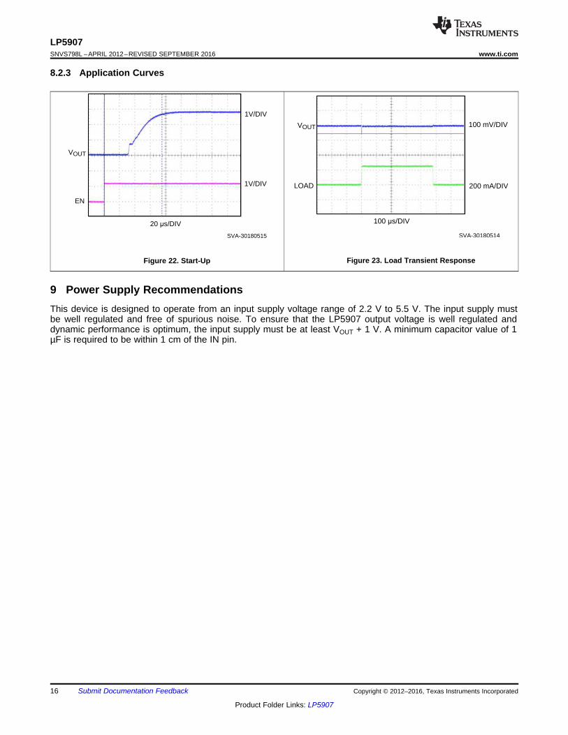
8.2.3 Application Curves
Figure 22. Start-Up Figure 23. Load Transient Response
9 Power Supply RecommendationsThis device is designed to operate from an input supply voltage range of 2.2 V to 5.5 V. The input supply mustbe well regulated and free of spurious noise. To ensure that the LP5907 output voltage is well regulated anddynamic performance is optimum, the input supply must be at least VOUT + 1 V. A minimum capacitor value of 1µF is required to be within 1 cm of the IN pin.
VINVOUT
Power GroundVEN
CINCOUT
LP5907SN
1
2 3
4
IN
GND
EN
OUT
N/C
CIN COUT1
2
3 4
5
VIN
GND
Enable
VOUT
GND
17
LP5907www.ti.com SNVS798L –APRIL 2012–REVISED SEPTEMBER 2016
Product Folder Links: LP5907
Submit Documentation FeedbackCopyright © 2012–2016, Texas Instruments Incorporated
10 Layout
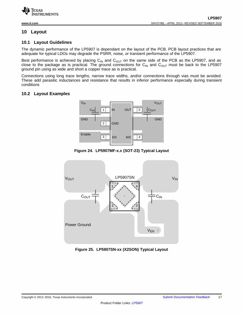
10.1 Layout GuidelinesThe dynamic performance of the LP5907 is dependant on the layout of the PCB. PCB layout practices that areadequate for typical LDOs may degrade the PSRR, noise, or transient performance of the LP5907.
Best performance is achieved by placing CIN and COUT on the same side of the PCB as the LP5907, and asclose to the package as is practical. The ground connections for CIN and COUT must be back to the LP5907ground pin using as wide and short a copper trace as is practical.
Connections using long trace lengths, narrow trace widths, and/or connections through vias must be avoided.These add parasitic inductances and resistance that results in inferior performance especially during transientconditions
10.2 Layout Examples
Figure 24. LP5907MF-x.x (SOT-23) Typical Layout
Figure 25. LP5907SN-xx (X2SON) Typical Layout
B2B1
A1 A2
VIN VOUT
Power GroundVEN
CIN COUT
LP5907UV
18
LP5907SNVS798L –APRIL 2012–REVISED SEPTEMBER 2016 www.ti.com
Product Folder Links: LP5907
Submit Documentation Feedback Copyright © 2012–2016, Texas Instruments Incorporated
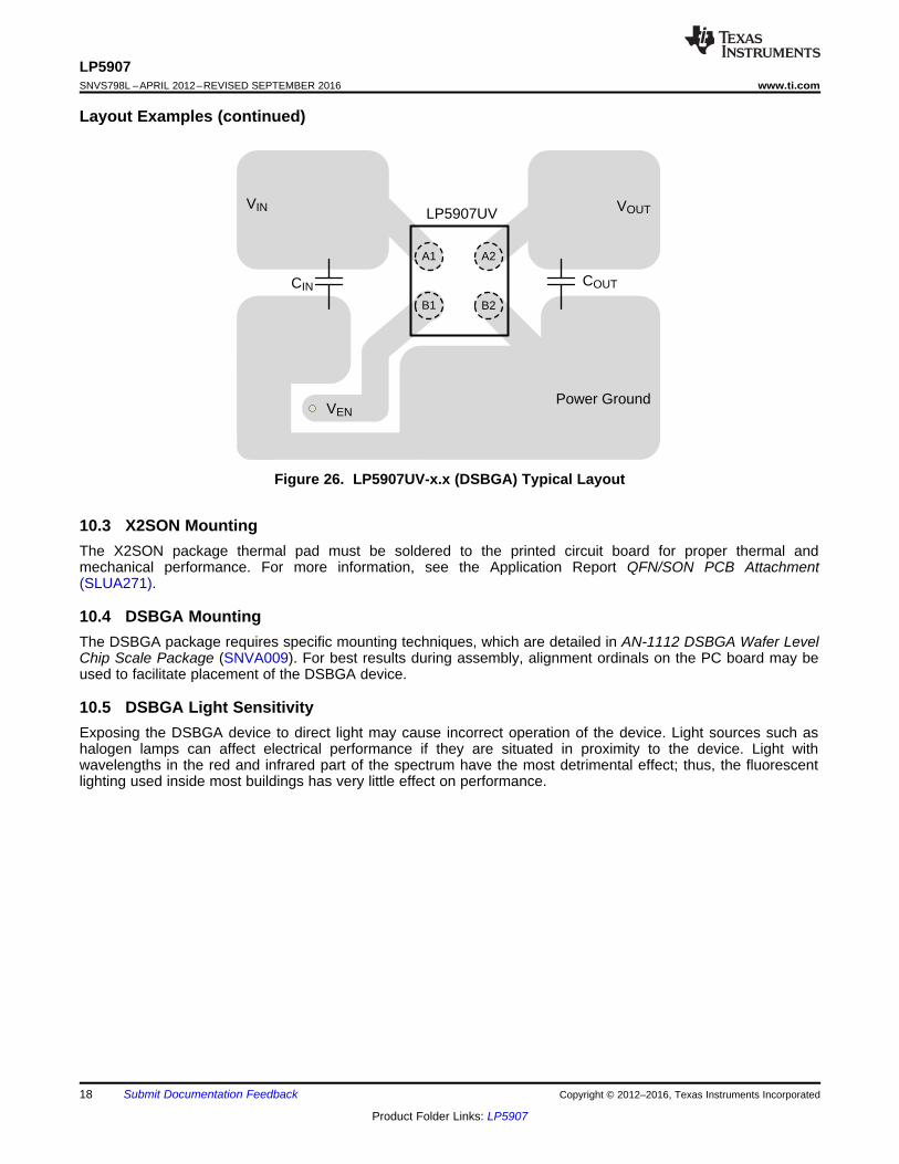
Layout Examples (continued)
Figure 26. LP5907UV-x.x (DSBGA) Typical Layout
10.3 X2SON MountingThe X2SON package thermal pad must be soldered to the printed circuit board for proper thermal andmechanical performance. For more information, see the Application Report QFN/SON PCB Attachment(SLUA271).
10.4 DSBGA MountingThe DSBGA package requires specific mounting techniques, which are detailed in AN-1112 DSBGA Wafer LevelChip Scale Package (SNVA009). For best results during assembly, alignment ordinals on the PC board may beused to facilitate placement of the DSBGA device.
10.5 DSBGA Light SensitivityExposing the DSBGA device to direct light may cause incorrect operation of the device. Light sources such ashalogen lamps can affect electrical performance if they are situated in proximity to the device. Light withwavelengths in the red and infrared part of the spectrum have the most detrimental effect; thus, the fluorescentlighting used inside most buildings has very little effect on performance.

19
LP5907www.ti.com SNVS798L –APRIL 2012–REVISED SEPTEMBER 2016
Product Folder Links: LP5907
Submit Documentation FeedbackCopyright © 2012–2016, Texas Instruments Incorporated
11 Device and Documentation Support
11.1 Documentation Support
11.1.1 Related DocumentationFor related documentation, see the following:• AN-1112 DSBGA Wafer Level Chip Scale Package (SNVA009)• Texas Instruments Application Report QFN/SON PCB Attachment (SLUA271)
11.2 Receiving Notification of Documentation UpdatesTo receive notification of documentation updates, navigate to the device product folder on ti.com. In the upperright corner, click on Alert me to register and receive a weekly digest of any product information that haschanged. For change details, review the revision history included in any revised document.
11.3 Community ResourcesThe following links connect to TI community resources. Linked contents are provided "AS IS" by the respectivecontributors. They do not constitute TI specifications and do not necessarily reflect TI's views; see TI's Terms ofUse.
TI E2E™ Online Community TI's Engineer-to-Engineer (E2E) Community. Created to foster collaborationamong engineers. At e2e.ti.com, you can ask questions, share knowledge, explore ideas and helpsolve problems with fellow engineers.
Design Support TI's Design Support Quickly find helpful E2E forums along with design support tools andcontact information for technical support.
11.4 TrademarksE2E is a trademark of Texas Instruments.All other trademarks are the property of their respective owners.
11.5 Electrostatic Discharge CautionThese devices have limited built-in ESD protection. The leads should be shorted together or the device placed in conductive foamduring storage or handling to prevent electrostatic damage to the MOS gates.
11.6 GlossarySLYZ022 — TI Glossary.
This glossary lists and explains terms, acronyms, and definitions.
12 Mechanical, Packaging, and Orderable InformationThe following pages include mechanical, packaging, and orderable information. This information is the mostcurrent data available for the designated devices. This data is subject to change without notice and revision ofthis document. For browser-based versions of this data sheet, refer to the left-hand navigation.
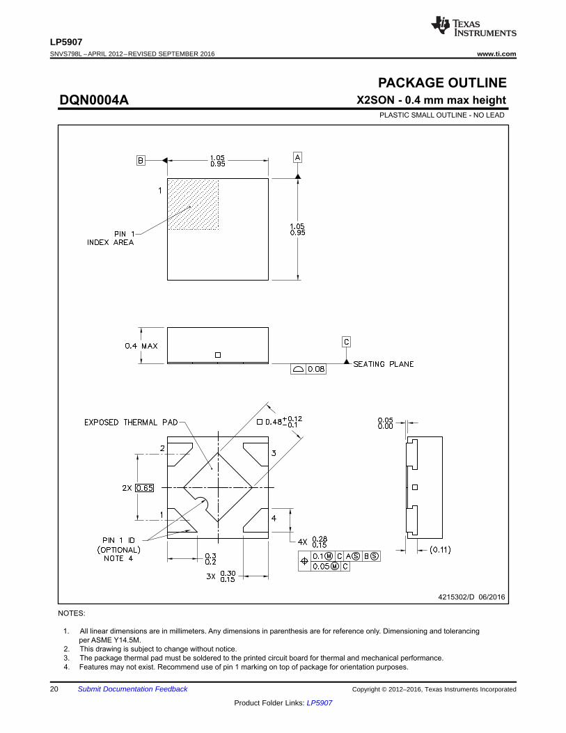
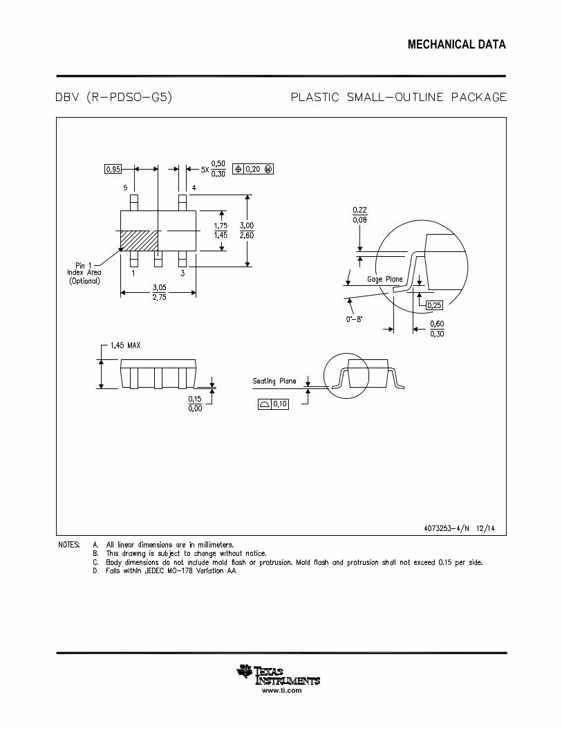
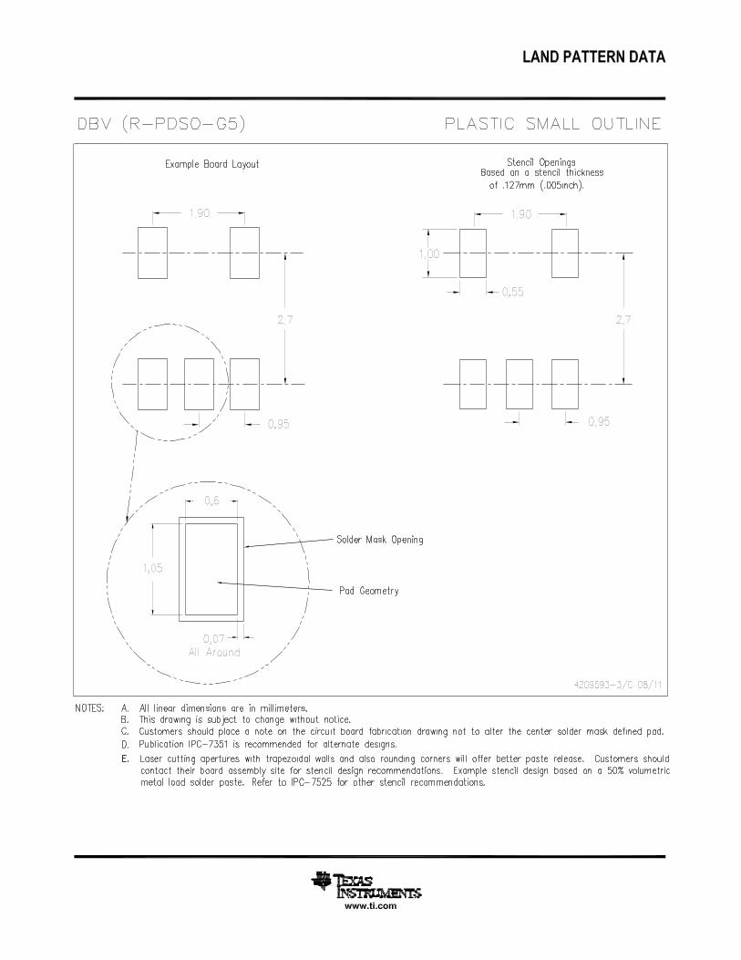
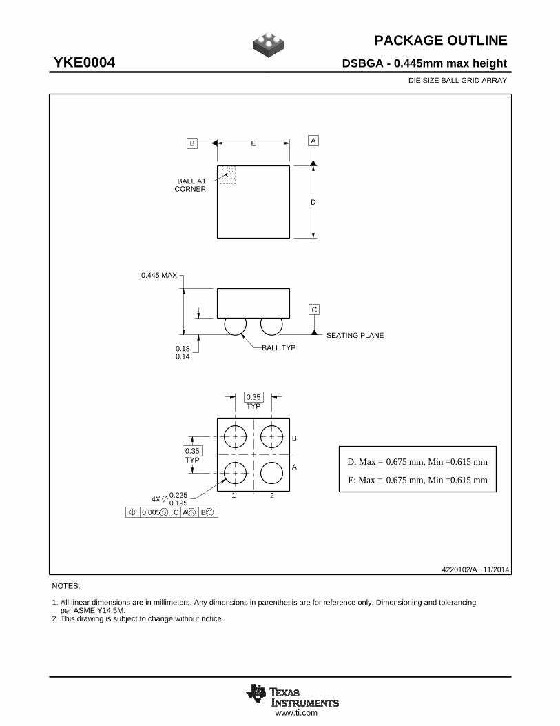
PACKAGE OUTLINE
DQN0004A X2SON - 0.4 mm max height
PLASTIC SMALL OUTLINE - NO LEAD
4215302/D 06/2016
NOTES:
1. All linear dimensions are in millimeters. Any dimensions in parenthesis are for reference only. Dimensioning and tolerancing
per ASME Y14.5M.
2. This drawing is subject to change without notice.
3. The package thermal pad must be soldered to the printed circuit board for thermal and mechanical performance.
4. Features may not exist. Recommend use of pin 1 marking on top of package for orientation purposes.
20
LP5907SNVS798L –APRIL 2012–REVISED SEPTEMBER 2016 www.ti.com
Product Folder Links: LP5907
Submit Documentation Feedback Copyright © 2012–2016, Texas Instruments Incorporated
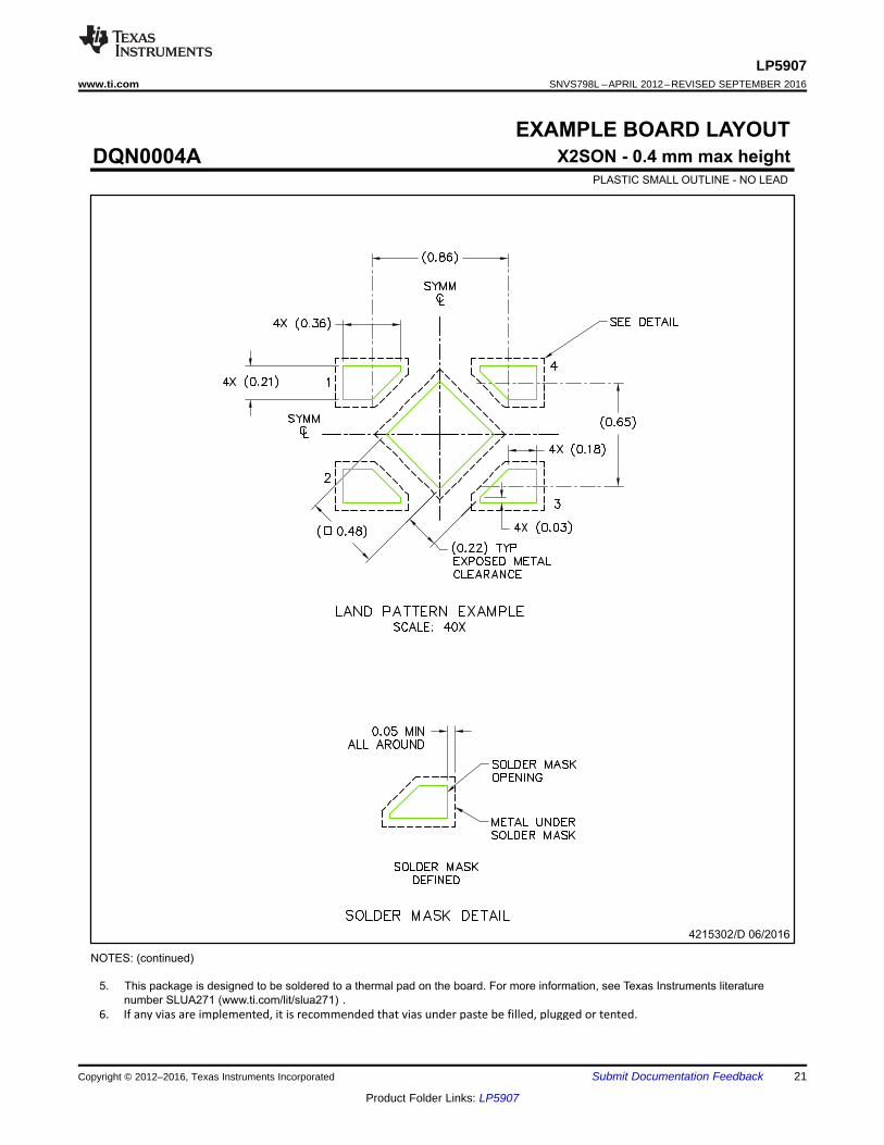
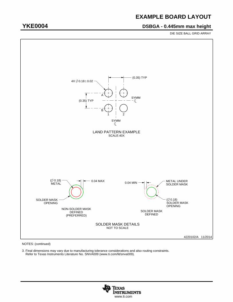
EXAMPLE BOARD LAYOUT
DQN0004A X2SON - 0.4 mm max height
PLASTIC SMALL OUTLINE - NO LEAD
4215302/D 06/2016
NOTES: (continued)
5. This package is designed to be soldered to a thermal pad on the board. For more information, see Texas Instruments literature
number SLUA271 (www.ti.com/lit/slua271) .
6. If any vias are implemented, it is recommended that vias under paste be filled, plugged or tented.
21
LP5907www.ti.com SNVS798L –APRIL 2012–REVISED SEPTEMBER 2016
Product Folder Links: LP5907
Submit Documentation FeedbackCopyright © 2012–2016, Texas Instruments Incorporated
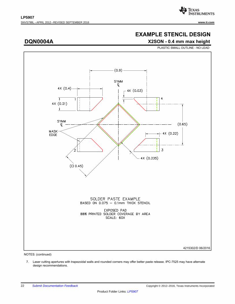
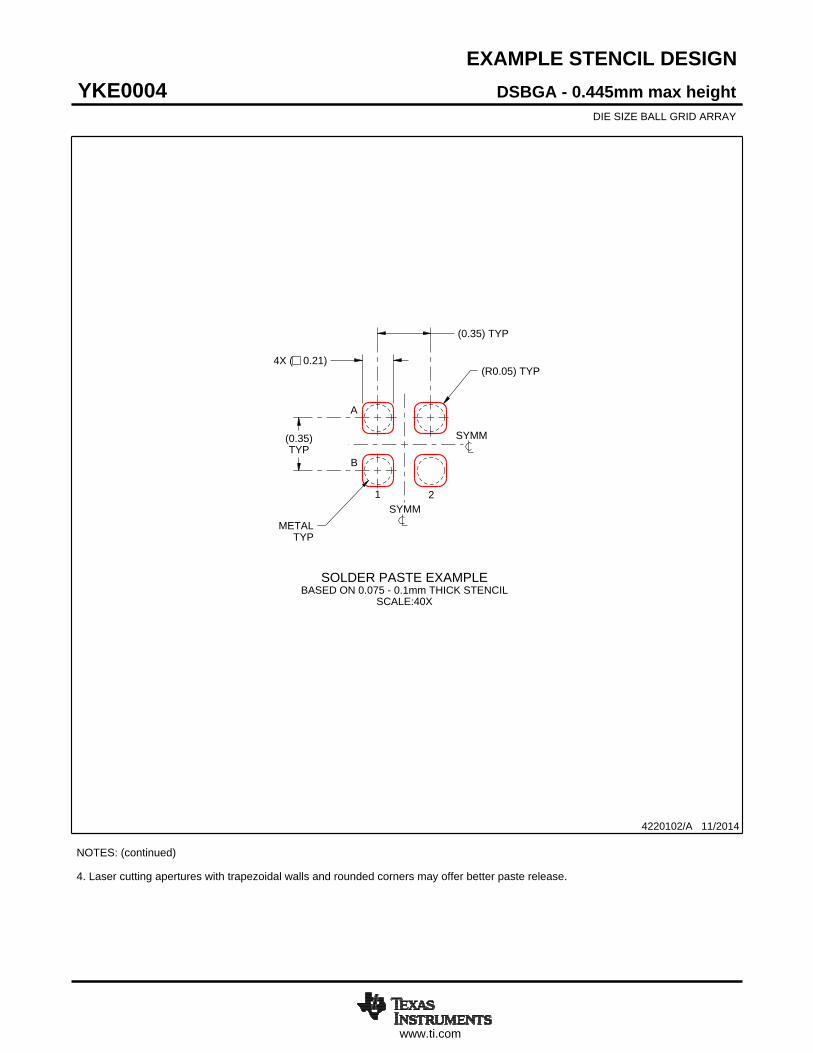
EXAMPLE STENCIL DESIGN
DQN0004A X2SON - 0.4 mm max height
PLASTIC SMALL OUTLINE - NO LEAD
4215302/D 06/2016
NOTES: (continued)
7. Laser cutting apertures with trapezoidal walls and rounded corners may offer better paste release. IPC-7525 may have alternate
design recommendations.
22
LP5907SNVS798L –APRIL 2012–REVISED SEPTEMBER 2016 www.ti.com
Product Folder Links: LP5907
Submit Documentation Feedback Copyright © 2012–2016, Texas Instruments Incorporated
PACKAGE OPTION ADDENDUM
www.ti.com 26-Aug-2016
Addendum-Page 1
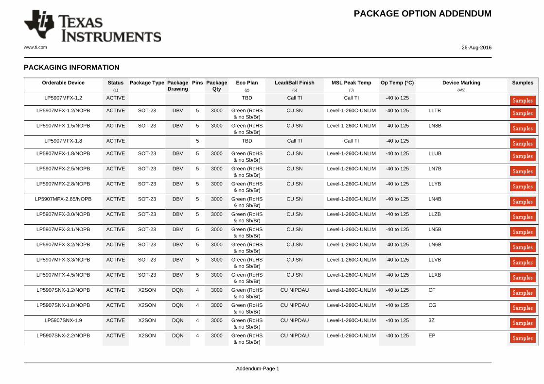
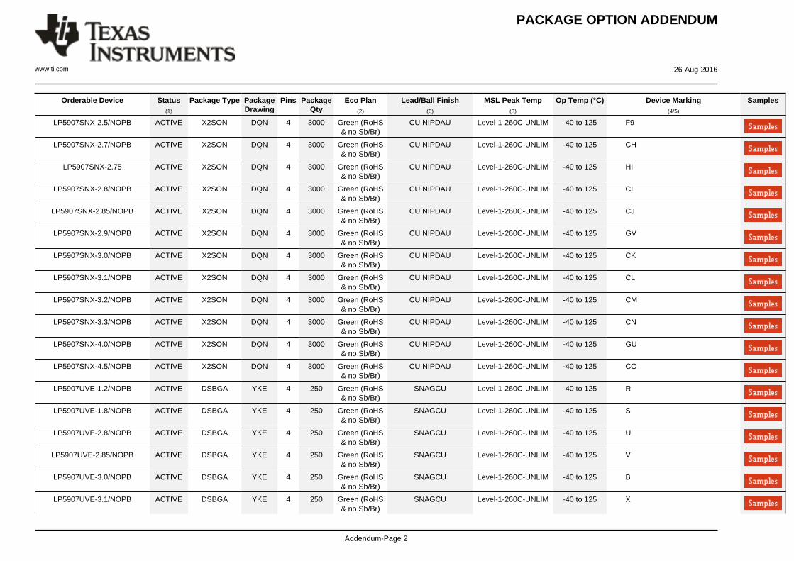
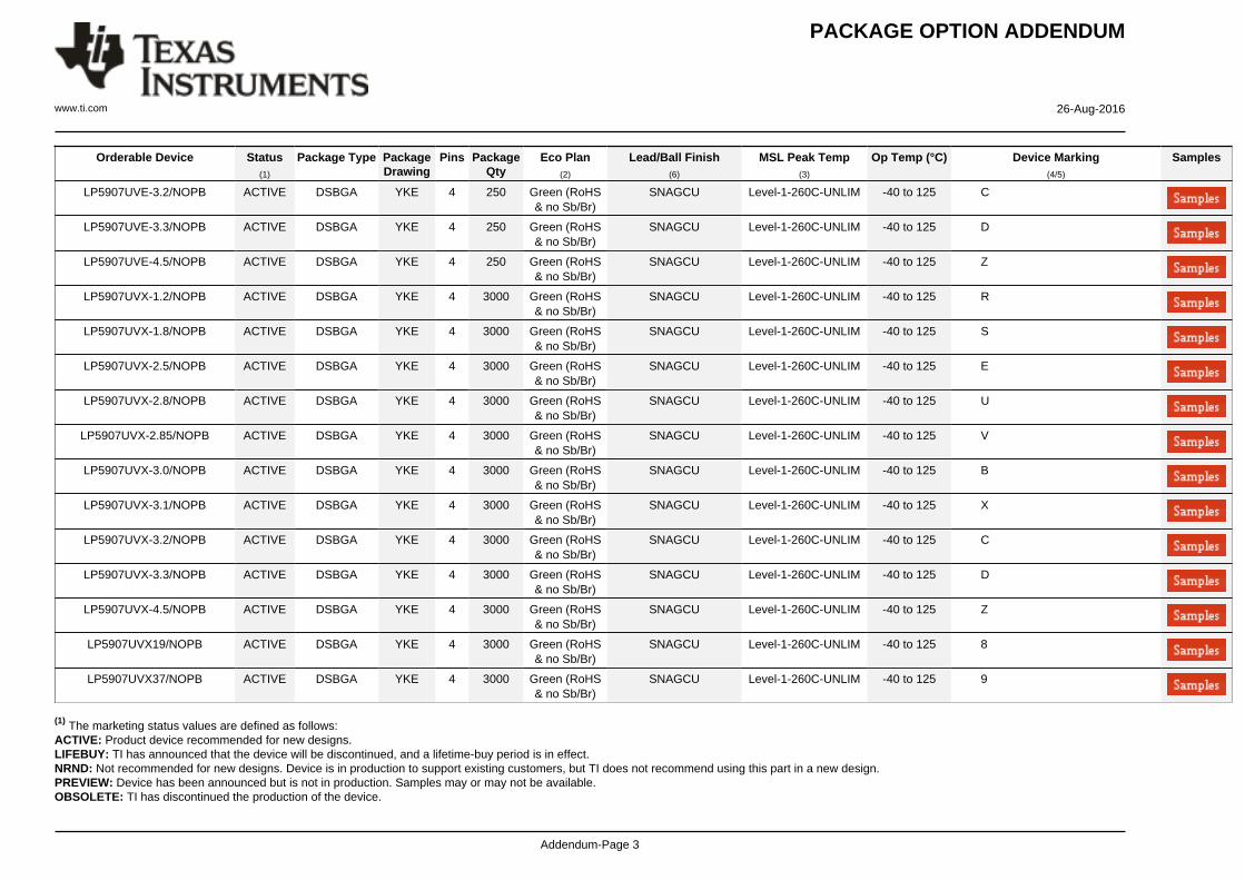
PACKAGING INFORMATION
Orderable Device Status(1)
Package Type PackageDrawing
Pins PackageQty
Eco Plan(2)
Lead/Ball Finish(6)
MSL Peak Temp(3)
Op Temp (°C) Device Marking(4/5)
Samples
LP5907MFX-1.2 ACTIVE TBD Call TI Call TI -40 to 125
LP5907MFX-1.2/NOPB ACTIVE SOT-23 DBV 5 3000 Green (RoHS& no Sb/Br)
CU SN Level-1-260C-UNLIM -40 to 125 LLTB
LP5907MFX-1.5/NOPB ACTIVE SOT-23 DBV 5 3000 Green (RoHS& no Sb/Br)
CU SN Level-1-260C-UNLIM -40 to 125 LN8B
LP5907MFX-1.8 ACTIVE 5 TBD Call TI Call TI -40 to 125
LP5907MFX-1.8/NOPB ACTIVE SOT-23 DBV 5 3000 Green (RoHS& no Sb/Br)
CU SN Level-1-260C-UNLIM -40 to 125 LLUB
LP5907MFX-2.5/NOPB ACTIVE SOT-23 DBV 5 3000 Green (RoHS& no Sb/Br)
CU SN Level-1-260C-UNLIM -40 to 125 LN7B
LP5907MFX-2.8/NOPB ACTIVE SOT-23 DBV 5 3000 Green (RoHS& no Sb/Br)
CU SN Level-1-260C-UNLIM -40 to 125 LLYB
LP5907MFX-2.85/NOPB ACTIVE SOT-23 DBV 5 3000 Green (RoHS& no Sb/Br)
CU SN Level-1-260C-UNLIM -40 to 125 LN4B
LP5907MFX-3.0/NOPB ACTIVE SOT-23 DBV 5 3000 Green (RoHS& no Sb/Br)
CU SN Level-1-260C-UNLIM -40 to 125 LLZB
LP5907MFX-3.1/NOPB ACTIVE SOT-23 DBV 5 3000 Green (RoHS& no Sb/Br)
CU SN Level-1-260C-UNLIM -40 to 125 LN5B
LP5907MFX-3.2/NOPB ACTIVE SOT-23 DBV 5 3000 Green (RoHS& no Sb/Br)
CU SN Level-1-260C-UNLIM -40 to 125 LN6B
LP5907MFX-3.3/NOPB ACTIVE SOT-23 DBV 5 3000 Green (RoHS& no Sb/Br)
CU SN Level-1-260C-UNLIM -40 to 125 LLVB
LP5907MFX-4.5/NOPB ACTIVE SOT-23 DBV 5 3000 Green (RoHS& no Sb/Br)
CU SN Level-1-260C-UNLIM -40 to 125 LLXB
LP5907SNX-1.2/NOPB ACTIVE X2SON DQN 4 3000 Green (RoHS& no Sb/Br)
CU NIPDAU Level-1-260C-UNLIM -40 to 125 CF
LP5907SNX-1.8/NOPB ACTIVE X2SON DQN 4 3000 Green (RoHS& no Sb/Br)
CU NIPDAU Level-1-260C-UNLIM -40 to 125 CG
LP5907SNX-1.9 ACTIVE X2SON DQN 4 3000 Green (RoHS& no Sb/Br)
CU NIPDAU Level-1-260C-UNLIM -40 to 125 3Z
LP5907SNX-2.2/NOPB ACTIVE X2SON DQN 4 3000 Green (RoHS& no Sb/Br)
CU NIPDAU Level-1-260C-UNLIM -40 to 125 EP
PACKAGE OPTION ADDENDUM
www.ti.com 26-Aug-2016
Addendum-Page 2
Orderable Device Status(1)
Package Type PackageDrawing
Pins PackageQty
Eco Plan(2)
Lead/Ball Finish(6)
MSL Peak Temp(3)
Op Temp (°C) Device Marking(4/5)
Samples
LP5907SNX-2.5/NOPB ACTIVE X2SON DQN 4 3000 Green (RoHS& no Sb/Br)
CU NIPDAU Level-1-260C-UNLIM -40 to 125 F9
LP5907SNX-2.7/NOPB ACTIVE X2SON DQN 4 3000 Green (RoHS& no Sb/Br)
CU NIPDAU Level-1-260C-UNLIM -40 to 125 CH
LP5907SNX-2.75 ACTIVE X2SON DQN 4 3000 Green (RoHS& no Sb/Br)
CU NIPDAU Level-1-260C-UNLIM -40 to 125 HI
LP5907SNX-2.8/NOPB ACTIVE X2SON DQN 4 3000 Green (RoHS& no Sb/Br)
CU NIPDAU Level-1-260C-UNLIM -40 to 125 CI
LP5907SNX-2.85/NOPB ACTIVE X2SON DQN 4 3000 Green (RoHS& no Sb/Br)
CU NIPDAU Level-1-260C-UNLIM -40 to 125 CJ
LP5907SNX-2.9/NOPB ACTIVE X2SON DQN 4 3000 Green (RoHS& no Sb/Br)
CU NIPDAU Level-1-260C-UNLIM -40 to 125 GV
LP5907SNX-3.0/NOPB ACTIVE X2SON DQN 4 3000 Green (RoHS& no Sb/Br)
CU NIPDAU Level-1-260C-UNLIM -40 to 125 CK
LP5907SNX-3.1/NOPB ACTIVE X2SON DQN 4 3000 Green (RoHS& no Sb/Br)
CU NIPDAU Level-1-260C-UNLIM -40 to 125 CL
LP5907SNX-3.2/NOPB ACTIVE X2SON DQN 4 3000 Green (RoHS& no Sb/Br)
CU NIPDAU Level-1-260C-UNLIM -40 to 125 CM
LP5907SNX-3.3/NOPB ACTIVE X2SON DQN 4 3000 Green (RoHS& no Sb/Br)
CU NIPDAU Level-1-260C-UNLIM -40 to 125 CN
LP5907SNX-4.0/NOPB ACTIVE X2SON DQN 4 3000 Green (RoHS& no Sb/Br)
CU NIPDAU Level-1-260C-UNLIM -40 to 125 GU
LP5907SNX-4.5/NOPB ACTIVE X2SON DQN 4 3000 Green (RoHS& no Sb/Br)
CU NIPDAU Level-1-260C-UNLIM -40 to 125 CO
LP5907UVE-1.2/NOPB ACTIVE DSBGA YKE 4 250 Green (RoHS& no Sb/Br)
SNAGCU Level-1-260C-UNLIM -40 to 125 R
LP5907UVE-1.8/NOPB ACTIVE DSBGA YKE 4 250 Green (RoHS& no Sb/Br)
SNAGCU Level-1-260C-UNLIM -40 to 125 S
LP5907UVE-2.8/NOPB ACTIVE DSBGA YKE 4 250 Green (RoHS& no Sb/Br)
SNAGCU Level-1-260C-UNLIM -40 to 125 U
LP5907UVE-2.85/NOPB ACTIVE DSBGA YKE 4 250 Green (RoHS& no Sb/Br)
SNAGCU Level-1-260C-UNLIM -40 to 125 V
LP5907UVE-3.0/NOPB ACTIVE DSBGA YKE 4 250 Green (RoHS& no Sb/Br)
SNAGCU Level-1-260C-UNLIM -40 to 125 B
LP5907UVE-3.1/NOPB ACTIVE DSBGA YKE 4 250 Green (RoHS& no Sb/Br)
SNAGCU Level-1-260C-UNLIM -40 to 125 X
PACKAGE OPTION ADDENDUM
www.ti.com 26-Aug-2016
Addendum-Page 3
Orderable Device Status(1)
Package Type PackageDrawing
Pins PackageQty
Eco Plan(2)
Lead/Ball Finish(6)
MSL Peak Temp(3)
Op Temp (°C) Device Marking(4/5)
Samples
LP5907UVE-3.2/NOPB ACTIVE DSBGA YKE 4 250 Green (RoHS& no Sb/Br)
SNAGCU Level-1-260C-UNLIM -40 to 125 C
LP5907UVE-3.3/NOPB ACTIVE DSBGA YKE 4 250 Green (RoHS& no Sb/Br)
SNAGCU Level-1-260C-UNLIM -40 to 125 D
LP5907UVE-4.5/NOPB ACTIVE DSBGA YKE 4 250 Green (RoHS& no Sb/Br)
SNAGCU Level-1-260C-UNLIM -40 to 125 Z
LP5907UVX-1.2/NOPB ACTIVE DSBGA YKE 4 3000 Green (RoHS& no Sb/Br)
SNAGCU Level-1-260C-UNLIM -40 to 125 R
LP5907UVX-1.8/NOPB ACTIVE DSBGA YKE 4 3000 Green (RoHS& no Sb/Br)
SNAGCU Level-1-260C-UNLIM -40 to 125 S
LP5907UVX-2.5/NOPB ACTIVE DSBGA YKE 4 3000 Green (RoHS& no Sb/Br)
SNAGCU Level-1-260C-UNLIM -40 to 125 E
LP5907UVX-2.8/NOPB ACTIVE DSBGA YKE 4 3000 Green (RoHS& no Sb/Br)
SNAGCU Level-1-260C-UNLIM -40 to 125 U
LP5907UVX-2.85/NOPB ACTIVE DSBGA YKE 4 3000 Green (RoHS& no Sb/Br)
SNAGCU Level-1-260C-UNLIM -40 to 125 V
LP5907UVX-3.0/NOPB ACTIVE DSBGA YKE 4 3000 Green (RoHS& no Sb/Br)
SNAGCU Level-1-260C-UNLIM -40 to 125 B
LP5907UVX-3.1/NOPB ACTIVE DSBGA YKE 4 3000 Green (RoHS& no Sb/Br)
SNAGCU Level-1-260C-UNLIM -40 to 125 X
LP5907UVX-3.2/NOPB ACTIVE DSBGA YKE 4 3000 Green (RoHS& no Sb/Br)
SNAGCU Level-1-260C-UNLIM -40 to 125 C
LP5907UVX-3.3/NOPB ACTIVE DSBGA YKE 4 3000 Green (RoHS& no Sb/Br)
SNAGCU Level-1-260C-UNLIM -40 to 125 D
LP5907UVX-4.5/NOPB ACTIVE DSBGA YKE 4 3000 Green (RoHS& no Sb/Br)
SNAGCU Level-1-260C-UNLIM -40 to 125 Z
LP5907UVX19/NOPB ACTIVE DSBGA YKE 4 3000 Green (RoHS& no Sb/Br)
SNAGCU Level-1-260C-UNLIM -40 to 125 8
LP5907UVX37/NOPB ACTIVE DSBGA YKE 4 3000 Green (RoHS& no Sb/Br)
SNAGCU Level-1-260C-UNLIM -40 to 125 9
(1) The marketing status values are defined as follows:ACTIVE: Product device recommended for new designs.LIFEBUY: TI has announced that the device will be discontinued, and a lifetime-buy period is in effect.NRND: Not recommended for new designs. Device is in production to support existing customers, but TI does not recommend using this part in a new design.PREVIEW: Device has been announced but is not in production. Samples may or may not be available.OBSOLETE: TI has discontinued the production of the device.

PACKAGE OPTION ADDENDUM
www.ti.com 26-Aug-2016
Addendum-Page 4
(2) Eco Plan - The planned eco-friendly classification: Pb-Free (RoHS), Pb-Free (RoHS Exempt), or Green (RoHS & no Sb/Br) - please check http://www.ti.com/productcontent for the latest availabilityinformation and additional product content details.TBD: The Pb-Free/Green conversion plan has not been defined.Pb-Free (RoHS): TI's terms "Lead-Free" or "Pb-Free" mean semiconductor products that are compatible with the current RoHS requirements for all 6 substances, including the requirement thatlead not exceed 0.1% by weight in homogeneous materials. Where designed to be soldered at high temperatures, TI Pb-Free products are suitable for use in specified lead-free processes.Pb-Free (RoHS Exempt): This component has a RoHS exemption for either 1) lead-based flip-chip solder bumps used between the die and package, or 2) lead-based die adhesive used betweenthe die and leadframe. The component is otherwise considered Pb-Free (RoHS compatible) as defined above.Green (RoHS & no Sb/Br): TI defines "Green" to mean Pb-Free (RoHS compatible), and free of Bromine (Br) and Antimony (Sb) based flame retardants (Br or Sb do not exceed 0.1% by weightin homogeneous material)
(3) MSL, Peak Temp. - The Moisture Sensitivity Level rating according to the JEDEC industry standard classifications, and peak solder temperature.
(4) There may be additional marking, which relates to the logo, the lot trace code information, or the environmental category on the device.
(5) Multiple Device Markings will be inside parentheses. Only one Device Marking contained in parentheses and separated by a "~" will appear on a device. If a line is indented then it is a continuationof the previous line and the two combined represent the entire Device Marking for that device.
(6) Lead/Ball Finish - Orderable Devices may have multiple material finish options. Finish options are separated by a vertical ruled line. Lead/Ball Finish values may wrap to two lines if the finishvalue exceeds the maximum column width.
Important Information and Disclaimer:The information provided on this page represents TI's knowledge and belief as of the date that it is provided. TI bases its knowledge and belief on informationprovided by third parties, and makes no representation or warranty as to the accuracy of such information. Efforts are underway to better integrate information from third parties. TI has taken andcontinues to take reasonable steps to provide representative and accurate information but may not have conducted destructive testing or chemical analysis on incoming materials and chemicals.TI and TI suppliers consider certain information to be proprietary, and thus CAS numbers and other limited information may not be available for release.
In no event shall TI's liability arising out of such information exceed the total purchase price of the TI part(s) at issue in this document sold by TI to Customer on an annual basis.
OTHER QUALIFIED VERSIONS OF LP5907 :
• Automotive: LP5907-Q1
NOTE: Qualified Version Definitions:
• Automotive - Q100 devices qualified for high-reliability automotive applications targeting zero defects

TAPE AND REEL INFORMATION
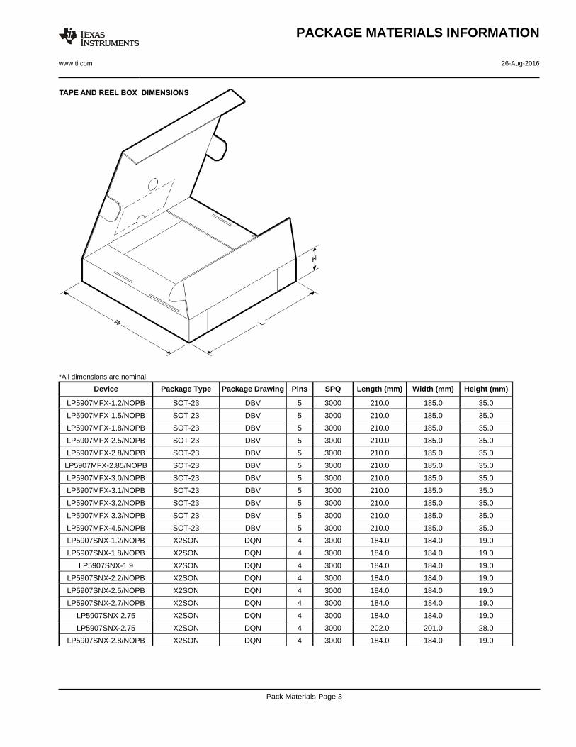
*All dimensions are nominal
Device PackageType
PackageDrawing
Pins SPQ ReelDiameter
(mm)
ReelWidth
W1 (mm)
A0(mm)
B0(mm)
K0(mm)
P1(mm)
W(mm)
Pin1Quadrant
LP5907MFX-1.2/NOPB SOT-23 DBV 5 3000 178.0 8.4 3.2 3.2 1.4 4.0 8.0 Q3
LP5907MFX-1.5/NOPB SOT-23 DBV 5 3000 178.0 8.4 3.2 3.2 1.4 4.0 8.0 Q3
LP5907MFX-1.8/NOPB SOT-23 DBV 5 3000 178.0 8.4 3.2 3.2 1.4 4.0 8.0 Q3
LP5907MFX-2.5/NOPB SOT-23 DBV 5 3000 178.0 8.4 3.2 3.2 1.4 4.0 8.0 Q3
LP5907MFX-2.8/NOPB SOT-23 DBV 5 3000 178.0 8.4 3.2 3.2 1.4 4.0 8.0 Q3
LP5907MFX-2.85/NOPB SOT-23 DBV 5 3000 178.0 8.4 3.2 3.2 1.4 4.0 8.0 Q3
LP5907MFX-3.0/NOPB SOT-23 DBV 5 3000 178.0 8.4 3.2 3.2 1.4 4.0 8.0 Q3
LP5907MFX-3.1/NOPB SOT-23 DBV 5 3000 178.0 8.4 3.2 3.2 1.4 4.0 8.0 Q3
LP5907MFX-3.2/NOPB SOT-23 DBV 5 3000 178.0 8.4 3.2 3.2 1.4 4.0 8.0 Q3
LP5907MFX-3.3/NOPB SOT-23 DBV 5 3000 178.0 8.4 3.2 3.2 1.4 4.0 8.0 Q3
LP5907MFX-4.5/NOPB SOT-23 DBV 5 3000 178.0 8.4 3.2 3.2 1.4 4.0 8.0 Q3
LP5907SNX-1.2/NOPB X2SON DQN 4 3000 180.0 9.5 1.16 1.16 0.63 4.0 8.0 Q2
LP5907SNX-1.8/NOPB X2SON DQN 4 3000 180.0 9.5 1.16 1.16 0.63 4.0 8.0 Q2
LP5907SNX-1.9 X2SON DQN 4 3000 180.0 9.5 1.16 1.16 0.63 4.0 8.0 Q2
LP5907SNX-2.2/NOPB X2SON DQN 4 3000 180.0 9.5 1.16 1.16 0.63 4.0 8.0 Q2
LP5907SNX-2.5/NOPB X2SON DQN 4 3000 180.0 9.5 1.16 1.16 0.63 4.0 8.0 Q2
LP5907SNX-2.7/NOPB X2SON DQN 4 3000 180.0 9.5 1.16 1.16 0.63 4.0 8.0 Q2
LP5907SNX-2.75 X2SON DQN 4 3000 180.0 9.5 1.16 1.16 0.63 4.0 8.0 Q2
PACKAGE MATERIALS INFORMATION
www.ti.com 26-Aug-2016
Pack Materials-Page 1

Device PackageType
PackageDrawing
Pins SPQ ReelDiameter
(mm)
ReelWidth
W1 (mm)
A0(mm)
B0(mm)
K0(mm)
P1(mm)
W(mm)
Pin1Quadrant
LP5907SNX-2.75 X2SON DQN 4 3000 180.0 8.4 1.16 1.16 0.63 4.0 8.0 Q2
LP5907SNX-2.8/NOPB X2SON DQN 4 3000 180.0 9.5 1.16 1.16 0.63 4.0 8.0 Q2
LP5907SNX-2.85/NOPB X2SON DQN 4 3000 180.0 9.5 1.16 1.16 0.63 4.0 8.0 Q2
LP5907SNX-2.85/NOPB X2SON DQN 4 3000 180.0 8.4 1.16 1.16 0.63 4.0 8.0 Q2
LP5907SNX-2.9/NOPB X2SON DQN 4 3000 180.0 9.5 1.16 1.16 0.63 4.0 8.0 Q2
LP5907SNX-3.0/NOPB X2SON DQN 4 3000 180.0 9.5 1.16 1.16 0.63 4.0 8.0 Q2
LP5907SNX-3.1/NOPB X2SON DQN 4 3000 180.0 9.5 1.16 1.16 0.63 4.0 8.0 Q2
LP5907SNX-3.2/NOPB X2SON DQN 4 3000 180.0 9.5 1.16 1.16 0.63 4.0 8.0 Q2
LP5907SNX-3.3/NOPB X2SON DQN 4 3000 180.0 9.5 1.16 1.16 0.63 4.0 8.0 Q2
LP5907SNX-4.0/NOPB X2SON DQN 4 3000 180.0 9.5 1.16 1.16 0.63 4.0 8.0 Q2
LP5907SNX-4.5/NOPB X2SON DQN 4 3000 180.0 9.5 1.16 1.16 0.63 4.0 8.0 Q2
LP5907UVE-1.2/NOPB DSBGA YKE 4 250 178.0 8.4 0.71 0.71 0.51 4.0 8.0 Q1
LP5907UVE-1.8/NOPB DSBGA YKE 4 250 178.0 8.4 0.71 0.71 0.51 4.0 8.0 Q1
LP5907UVE-2.8/NOPB DSBGA YKE 4 250 178.0 8.4 0.71 0.71 0.51 4.0 8.0 Q1
LP5907UVE-2.85/NOPB DSBGA YKE 4 250 178.0 8.4 0.71 0.71 0.51 4.0 8.0 Q1
LP5907UVE-3.0/NOPB DSBGA YKE 4 250 178.0 8.4 0.71 0.71 0.51 4.0 8.0 Q1
LP5907UVE-3.1/NOPB DSBGA YKE 4 250 178.0 8.4 0.71 0.71 0.51 4.0 8.0 Q1
LP5907UVE-3.2/NOPB DSBGA YKE 4 250 178.0 8.4 0.71 0.71 0.51 4.0 8.0 Q1
LP5907UVE-3.3/NOPB DSBGA YKE 4 250 178.0 8.4 0.71 0.71 0.51 4.0 8.0 Q1
LP5907UVE-4.5/NOPB DSBGA YKE 4 250 178.0 8.4 0.71 0.71 0.51 4.0 8.0 Q1
LP5907UVX-1.2/NOPB DSBGA YKE 4 3000 178.0 8.4 0.71 0.71 0.51 4.0 8.0 Q1
LP5907UVX-1.8/NOPB DSBGA YKE 4 3000 178.0 8.4 0.7 0.7 0.48 4.0 8.0 Q1
LP5907UVX-1.8/NOPB DSBGA YKE 4 3000 178.0 8.4 0.71 0.71 0.51 4.0 8.0 Q1
LP5907UVX-2.5/NOPB DSBGA YKE 4 3000 178.0 8.4 0.71 0.71 0.51 4.0 8.0 Q1
LP5907UVX-2.8/NOPB DSBGA YKE 4 3000 178.0 8.4 0.71 0.71 0.51 4.0 8.0 Q1
LP5907UVX-2.85/NOPB DSBGA YKE 4 3000 178.0 8.4 0.7 0.7 0.48 4.0 8.0 Q1
LP5907UVX-2.85/NOPB DSBGA YKE 4 3000 178.0 8.4 0.71 0.71 0.51 4.0 8.0 Q1
LP5907UVX-3.0/NOPB DSBGA YKE 4 3000 178.0 8.4 0.71 0.71 0.51 4.0 8.0 Q1
LP5907UVX-3.1/NOPB DSBGA YKE 4 3000 178.0 8.4 0.71 0.71 0.51 4.0 8.0 Q1
LP5907UVX-3.2/NOPB DSBGA YKE 4 3000 178.0 8.4 0.71 0.71 0.51 4.0 8.0 Q1
LP5907UVX-3.3/NOPB DSBGA YKE 4 3000 178.0 8.4 0.71 0.71 0.51 4.0 8.0 Q1
LP5907UVX-4.5/NOPB DSBGA YKE 4 3000 178.0 8.4 0.71 0.71 0.51 4.0 8.0 Q1
LP5907UVX19/NOPB DSBGA YKE 4 3000 178.0 8.4 0.71 0.71 0.51 4.0 8.0 Q1
LP5907UVX19/NOPB DSBGA YKE 4 3000 178.0 8.4 0.7 0.7 0.48 4.0 8.0 Q1
LP5907UVX37/NOPB DSBGA YKE 4 3000 178.0 8.4 0.71 0.71 0.51 4.0 8.0 Q1
PACKAGE MATERIALS INFORMATION
www.ti.com 26-Aug-2016
Pack Materials-Page 2
*All dimensions are nominal
Device Package Type Package Drawing Pins SPQ Length (mm) Width (mm) Height (mm)
LP5907MFX-1.2/NOPB SOT-23 DBV 5 3000 210.0 185.0 35.0
LP5907MFX-1.5/NOPB SOT-23 DBV 5 3000 210.0 185.0 35.0
LP5907MFX-1.8/NOPB SOT-23 DBV 5 3000 210.0 185.0 35.0
LP5907MFX-2.5/NOPB SOT-23 DBV 5 3000 210.0 185.0 35.0
LP5907MFX-2.8/NOPB SOT-23 DBV 5 3000 210.0 185.0 35.0
LP5907MFX-2.85/NOPB SOT-23 DBV 5 3000 210.0 185.0 35.0
LP5907MFX-3.0/NOPB SOT-23 DBV 5 3000 210.0 185.0 35.0
LP5907MFX-3.1/NOPB SOT-23 DBV 5 3000 210.0 185.0 35.0
LP5907MFX-3.2/NOPB SOT-23 DBV 5 3000 210.0 185.0 35.0
LP5907MFX-3.3/NOPB SOT-23 DBV 5 3000 210.0 185.0 35.0
LP5907MFX-4.5/NOPB SOT-23 DBV 5 3000 210.0 185.0 35.0
LP5907SNX-1.2/NOPB X2SON DQN 4 3000 184.0 184.0 19.0
LP5907SNX-1.8/NOPB X2SON DQN 4 3000 184.0 184.0 19.0
LP5907SNX-1.9 X2SON DQN 4 3000 184.0 184.0 19.0
LP5907SNX-2.2/NOPB X2SON DQN 4 3000 184.0 184.0 19.0
LP5907SNX-2.5/NOPB X2SON DQN 4 3000 184.0 184.0 19.0
LP5907SNX-2.7/NOPB X2SON DQN 4 3000 184.0 184.0 19.0
LP5907SNX-2.75 X2SON DQN 4 3000 184.0 184.0 19.0
LP5907SNX-2.75 X2SON DQN 4 3000 202.0 201.0 28.0
LP5907SNX-2.8/NOPB X2SON DQN 4 3000 184.0 184.0 19.0
PACKAGE MATERIALS INFORMATION
www.ti.com 26-Aug-2016
Pack Materials-Page 3
Device Package Type Package Drawing Pins SPQ Length (mm) Width (mm) Height (mm)
LP5907SNX-2.85/NOPB X2SON DQN 4 3000 184.0 184.0 19.0
LP5907SNX-2.85/NOPB X2SON DQN 4 3000 202.0 201.0 28.0
LP5907SNX-2.9/NOPB X2SON DQN 4 3000 184.0 184.0 19.0
LP5907SNX-3.0/NOPB X2SON DQN 4 3000 184.0 184.0 19.0
LP5907SNX-3.1/NOPB X2SON DQN 4 3000 184.0 184.0 19.0
LP5907SNX-3.2/NOPB X2SON DQN 4 3000 184.0 184.0 19.0
LP5907SNX-3.3/NOPB X2SON DQN 4 3000 184.0 184.0 19.0
LP5907SNX-4.0/NOPB X2SON DQN 4 3000 184.0 184.0 19.0
LP5907SNX-4.5/NOPB X2SON DQN 4 3000 184.0 184.0 19.0
LP5907UVE-1.2/NOPB DSBGA YKE 4 250 210.0 185.0 35.0
LP5907UVE-1.8/NOPB DSBGA YKE 4 250 210.0 185.0 35.0
LP5907UVE-2.8/NOPB DSBGA YKE 4 250 210.0 185.0 35.0
LP5907UVE-2.85/NOPB DSBGA YKE 4 250 210.0 185.0 35.0
LP5907UVE-3.0/NOPB DSBGA YKE 4 250 210.0 185.0 35.0
LP5907UVE-3.1/NOPB DSBGA YKE 4 250 210.0 185.0 35.0
LP5907UVE-3.2/NOPB DSBGA YKE 4 250 210.0 185.0 35.0
LP5907UVE-3.3/NOPB DSBGA YKE 4 250 210.0 185.0 35.0
LP5907UVE-4.5/NOPB DSBGA YKE 4 250 210.0 185.0 35.0
LP5907UVX-1.2/NOPB DSBGA YKE 4 3000 210.0 185.0 35.0
LP5907UVX-1.8/NOPB DSBGA YKE 4 3000 220.0 220.0 35.0
LP5907UVX-1.8/NOPB DSBGA YKE 4 3000 210.0 185.0 35.0
LP5907UVX-2.5/NOPB DSBGA YKE 4 3000 210.0 185.0 35.0
LP5907UVX-2.8/NOPB DSBGA YKE 4 3000 210.0 185.0 35.0
LP5907UVX-2.85/NOPB DSBGA YKE 4 3000 220.0 220.0 35.0
LP5907UVX-2.85/NOPB DSBGA YKE 4 3000 210.0 185.0 35.0
LP5907UVX-3.0/NOPB DSBGA YKE 4 3000 210.0 185.0 35.0
LP5907UVX-3.1/NOPB DSBGA YKE 4 3000 210.0 185.0 35.0
LP5907UVX-3.2/NOPB DSBGA YKE 4 3000 210.0 185.0 35.0
LP5907UVX-3.3/NOPB DSBGA YKE 4 3000 210.0 185.0 35.0
LP5907UVX-4.5/NOPB DSBGA YKE 4 3000 210.0 185.0 35.0
LP5907UVX19/NOPB DSBGA YKE 4 3000 210.0 185.0 35.0
LP5907UVX19/NOPB DSBGA YKE 4 3000 220.0 220.0 35.0
LP5907UVX37/NOPB DSBGA YKE 4 3000 210.0 185.0 35.0
PACKAGE MATERIALS INFORMATION
www.ti.com 26-Aug-2016
Pack Materials-Page 4
www.ti.com
PACKAGE OUTLINE
C
0.445 MAX
0.180.14
0.35TYP
0.35TYP
4X 0.2250.195
B E A
D
4220102/A 11/2014
DSBGA - 0.445mm max heightYKE0004DIE SIZE BALL GRID ARRAY
NOTES: 1. All linear dimensions are in millimeters. Any dimensions in parenthesis are for reference only. Dimensioning and tolerancing per ASME Y14.5M. 2. This drawing is subject to change without notice.
BALL A1CORNER
SEATING PLANE
BALL TYP
B
A
1 2
0.005 C A B
SCALE 12.000
D: Max =
E: Max =
0.675 mm, Min =
0.675 mm, Min =
0.615 mm
0.615 mm
www.ti.com
EXAMPLE BOARD LAYOUT
4X 0.18 0.02(0.35) TYP
(0.35) TYP
( )METAL
0.18 0.04 MAX
SOLDER MASKOPENING
METAL UNDERSOLDER MASK
( )SOLDER MASKOPENING
0.18
0.04 MIN
4220102/A 11/2014
DSBGA - 0.445mm max heightYKE0004DIE SIZE BALL GRID ARRAY
NOTES: (continued) 3. Final dimensions may vary due to manufacturing tolerance considerations and also routing constraints. Refer to Texas Instruments Literature No. SNVA009 (www.ti.com/lit/snva009).
SOLDER MASK DETAILSNOT TO SCALE
1
SYMM
SYMM
LAND PATTERN EXAMPLESCALE:40X
2
A
B
NON-SOLDER MASKDEFINED
(PREFERRED)SOLDER MASK
DEFINED
www.ti.com
EXAMPLE STENCIL DESIGN
(0.35)TYP
(0.35) TYP
4X ( 0.21)(R ) TYP0.05
METALTYP
4220102/A 11/2014
DSBGA - 0.445mm max heightYKE0004DIE SIZE BALL GRID ARRAY
NOTES: (continued) 4. Laser cutting apertures with trapezoidal walls and rounded corners may offer better paste release.
1 2
A
B
SYMM
SYMM
SOLDER PASTE EXAMPLEBASED ON 0.075 - 0.1mm THICK STENCIL
SCALE:40X

IMPORTANT NOTICE
Texas Instruments Incorporated and its subsidiaries (TI) reserve the right to make corrections, enhancements, improvements and otherchanges to its semiconductor products and services per JESD46, latest issue, and to discontinue any product or service per JESD48, latestissue. Buyers should obtain the latest relevant information before placing orders and should verify that such information is current andcomplete. All semiconductor products (also referred to herein as “components”) are sold subject to TI’s terms and conditions of salesupplied at the time of order acknowledgment.TI warrants performance of its components to the specifications applicable at the time of sale, in accordance with the warranty in TI’s termsand conditions of sale of semiconductor products. Testing and other quality control techniques are used to the extent TI deems necessaryto support this warranty. Except where mandated by applicable law, testing of all parameters of each component is not necessarilyperformed.TI assumes no liability for applications assistance or the design of Buyers’ products. Buyers are responsible for their products andapplications using TI components. To minimize the risks associated with Buyers’ products and applications, Buyers should provideadequate design and operating safeguards.TI does not warrant or represent that any license, either express or implied, is granted under any patent right, copyright, mask work right, orother intellectual property right relating to any combination, machine, or process in which TI components or services are used. Informationpublished by TI regarding third-party products or services does not constitute a license to use such products or services or a warranty orendorsement thereof. Use of such information may require a license from a third party under the patents or other intellectual property of thethird party, or a license from TI under the patents or other intellectual property of TI.Reproduction of significant portions of TI information in TI data books or data sheets is permissible only if reproduction is without alterationand is accompanied by all associated warranties, conditions, limitations, and notices. TI is not responsible or liable for such altereddocumentation. Information of third parties may be subject to additional restrictions.Resale of TI components or services with statements different from or beyond the parameters stated by TI for that component or servicevoids all express and any implied warranties for the associated TI component or service and is an unfair and deceptive business practice.TI is not responsible or liable for any such statements.Buyer acknowledges and agrees that it is solely responsible for compliance with all legal, regulatory and safety-related requirementsconcerning its products, and any use of TI components in its applications, notwithstanding any applications-related information or supportthat may be provided by TI. Buyer represents and agrees that it has all the necessary expertise to create and implement safeguards whichanticipate dangerous consequences of failures, monitor failures and their consequences, lessen the likelihood of failures that might causeharm and take appropriate remedial actions. Buyer will fully indemnify TI and its representatives against any damages arising out of the useof any TI components in safety-critical applications.In some cases, TI components may be promoted specifically to facilitate safety-related applications. With such components, TI’s goal is tohelp enable customers to design and create their own end-product solutions that meet applicable functional safety standards andrequirements. Nonetheless, such components are subject to these terms.No TI components are authorized for use in FDA Class III (or similar life-critical medical equipment) unless authorized officers of the partieshave executed a special agreement specifically governing such use.Only those TI components which TI has specifically designated as military grade or “enhanced plastic” are designed and intended for use inmilitary/aerospace applications or environments. Buyer acknowledges and agrees that any military or aerospace use of TI componentswhich have not been so designated is solely at the Buyer's risk, and that Buyer is solely responsible for compliance with all legal andregulatory requirements in connection with such use.TI has specifically designated certain components as meeting ISO/TS16949 requirements, mainly for automotive use. In any case of use ofnon-designated products, TI will not be responsible for any failure to meet ISO/TS16949.
Products ApplicationsAudio www.ti.com/audio Automotive and Transportation www.ti.com/automotiveAmplifiers amplifier.ti.com Communications and Telecom www.ti.com/communicationsData Converters dataconverter.ti.com Computers and Peripherals www.ti.com/computersDLP® Products www.dlp.com Consumer Electronics www.ti.com/consumer-appsDSP dsp.ti.com Energy and Lighting www.ti.com/energyClocks and Timers www.ti.com/clocks Industrial www.ti.com/industrialInterface interface.ti.com Medical www.ti.com/medicalLogic logic.ti.com Security www.ti.com/securityPower Mgmt power.ti.com Space, Avionics and Defense www.ti.com/space-avionics-defenseMicrocontrollers microcontroller.ti.com Video and Imaging www.ti.com/videoRFID www.ti-rfid.comOMAP Applications Processors www.ti.com/omap TI E2E Community e2e.ti.comWireless Connectivity www.ti.com/wirelessconnectivity
Mailing Address: Texas Instruments, Post Office Box 655303, Dallas, Texas 75265Copyright © 2016, Texas Instruments Incorporated