Embed Size (px)
Citation preview
EN
IN OUT
GND
1 PF 1 PF
INPUT
ENABLE
GND
OUTPUT
LP5907-Q1
Product
Folder
Order
Now
Technical
Documents
Tools &
Software
Support &Community
ReferenceDesign
An IMPORTANT NOTICE at the end of this data sheet addresses availability, warranty, changes, use in safety-critical applications,intellectual property matters and other important disclaimers. PRODUCTION DATA.
LP5907-Q1SNVSA34C –SEPTEMBER 2014–REVISED MAY 2018
LP5907-Q1 Automotive 250-mA, Ultra-Low-Noise, Low-IQ LDO
1
1 Features1• Qualified for Automotive Applications• AEC-Q100 Qualified With the Following Results:
– Device Temperature Grade 1: –40°C to 125°CAmbient Operating Temperature Range
– Device HBM ESD Classification Level 2– Device CDM ESD Classification Level C6
• Input Voltage Range: 2.2 V to 5.5 V• Output Voltage Range: 1.2 V to 4.5 V• Stable with 1-µF Ceramic Input and Output
Capacitors• No Noise Bypass Capacitor Required• Remote Output Capacitor Placement• Thermal-Overload and Short-Circuit Protection• Output Current: 250 mA• Low Output Voltage Noise: < 6.5 µVRMS
• PSRR: 82 dB at 1 kHz• Output Voltage Tolerance: ±2%• Virtually Zero IQ (Disabled): < 1 µA• Very Low IQ (Enabled): 12 µA• Start-up Time: 80 µs• Low Dropout: 120 mV (Typical)• –40°C to 125°C Junction Temperature Range for
Operation
2 Applications• Automotive Infotainment• Telematics Systems• ADAS Cameras and Radar• Navigation Systems
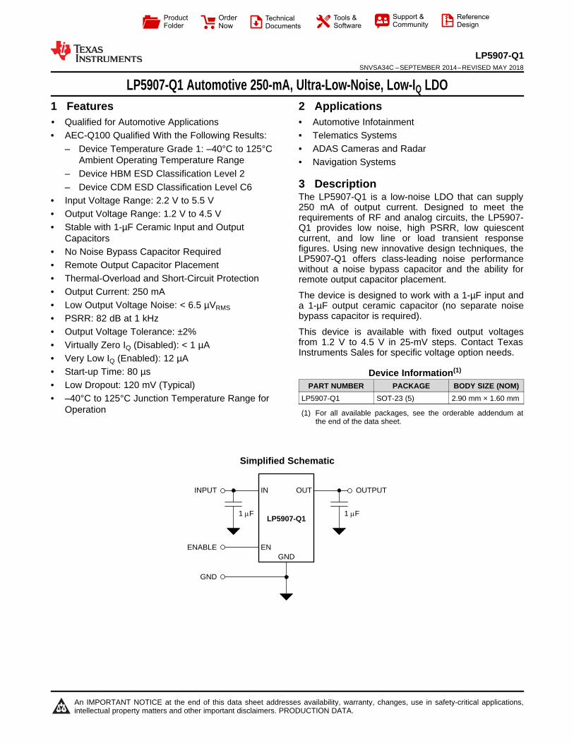
3 DescriptionThe LP5907-Q1 is a low-noise LDO that can supply250 mA of output current. Designed to meet therequirements of RF and analog circuits, the LP5907-Q1 provides low noise, high PSRR, low quiescentcurrent, and low line or load transient responsefigures. Using new innovative design techniques, theLP5907-Q1 offers class-leading noise performancewithout a noise bypass capacitor and the ability forremote output capacitor placement.
The device is designed to work with a 1-µF input anda 1-µF output ceramic capacitor (no separate noisebypass capacitor is required).
This device is available with fixed output voltagesfrom 1.2 V to 4.5 V in 25-mV steps. Contact TexasInstruments Sales for specific voltage option needs.
Device Information(1)
PART NUMBER PACKAGE BODY SIZE (NOM)LP5907-Q1 SOT-23 (5) 2.90 mm × 1.60 mm
(1) For all available packages, see the orderable addendum atthe end of the data sheet.
Simplified Schematic
2
LP5907-Q1SNVSA34C –SEPTEMBER 2014–REVISED MAY 2018 www.ti.com
Product Folder Links: LP5907-Q1
Submit Documentation Feedback Copyright © 2014–2018, Texas Instruments Incorporated
Table of Contents1 Features .................................................................. 12 Applications ........................................................... 13 Description ............................................................. 14 Revision History..................................................... 25 Pin Configuration and Functions ......................... 36 Specifications......................................................... 4
6.1 Absolute Maximum Ratings ...................................... 46.2 ESD Ratings.............................................................. 46.3 Recommended Operating Conditions....................... 46.4 Thermal Information .................................................. 46.5 Electrical Characteristics........................................... 56.6 Output and Input Capacitors ..................................... 66.7 Typical Characteristics .............................................. 7
7 Detailed Description ............................................ 117.1 Overview ................................................................. 117.2 Functional Block Diagram ....................................... 11
7.3 Feature Description................................................. 127.4 Device Functional Modes........................................ 13
8 Application and Implementation ........................ 148.1 Application Information............................................ 148.2 Typical Application .................................................. 14
9 Power Supply Recommendations ...................... 1710 Layout................................................................... 17
10.1 Layout Guidelines ................................................. 1710.2 Layout Example .................................................... 17
11 Device and Documentation Support ................. 1811.1 Receiving Notification of Documentation Updates 1811.2 Community Resources.......................................... 1811.3 Trademarks ........................................................... 1811.4 Electrostatic Discharge Caution............................ 1811.5 Glossary ................................................................ 18
12 Mechanical, Packaging, and OrderableInformation ........................................................... 18
4 Revision HistoryNOTE: Page numbers for previous revisions may differ from page numbers in the current version.
Changes from Revision B (September 2016) to Revision C Page
• Added ESD classification level sub-bullets to Features section ............................................................................................ 1• Changed DBV values in Thermal Information table .............................................................................................................. 4• Deleted footnote 1 from Thermal Information table ............................................................................................................... 4• Added Overshoot on start-up with EN row to Electrical Characteristics table ...................................................................... 6• Changed Device Comparison table: changed table title, added new rows and new data, moved to new sub-section ...... 12
Changes from Revision A (June 2016) to Revision B Page
• Changed wording of title ........................................................................................................................................................ 1• Changed "Low Output Voltage Noise: < 10 µVRMS" to "Low Output Voltage Noise: < 6.5 µVRMS"......................................... 1• Changed items listed in Applications ..................................................................................................................................... 1• Changed wording of first sentence of Description ................................................................................................................. 1
Changes from Original (September 2014) to Revision A Page
• Added Features bullets re: automotive .................................................................................................................................. 1• Added top navigator icon for TI Designs ................................................................................................................................ 1• Changed " linear regulator" to "LDO" ..................................................................................................................................... 1• Changed storage temperature from Handling Ratings to Abs Max table; replaced Handling Ratings with ESD
Ratings per new format ......................................................................................................................................................... 4
N/C
1
2
3
5
4EN
GND
IN OUT
3
LP5907-Q1www.ti.com SNVSA34C –SEPTEMBER 2014–REVISED MAY 2018
Product Folder Links: LP5907-Q1
Submit Documentation FeedbackCopyright © 2014–2018, Texas Instruments Incorporated
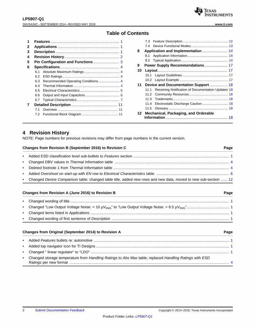
5 Pin Configuration and Functions
DBV Package5-Pin SOT-23
(Top View)
Pin FunctionsPIN
I/O DESCRIPTIONNAME SOT23-5
IN 1 I Input voltage supply. Connect a 1-µF capacitor at this input.GND 2 – Common ground
EN 3 I
Enable input. A low voltage (< VIL) on this pin turns the regulator off and discharges theoutput pin to GND through an internal 230-Ω pulldown resistor. A high voltage (> VIH) onthis pin enables the regulator output. This pin has an internal 1-MΩ pulldown resistor tohold the regulator off by default.
N/C 4 – No internal electrical connection.
OUT 5 ORegulated output voltage. Connect a minimum 1-µF low-ESR capacitor to this pin. Connectthis output to the load circuit. An internal 230-Ω (typical) pulldown resistor prevents acharge remaining on VOUT when the regulator is in the shutdown mode (VEN low).
4
LP5907-Q1SNVSA34C –SEPTEMBER 2014–REVISED MAY 2018 www.ti.com
Product Folder Links: LP5907-Q1
Submit Documentation Feedback Copyright © 2014–2018, Texas Instruments Incorporated
(1) Stresses beyond those listed under Absolute Maximum Ratings may cause permanent damage to the device. These are stress ratingsonly, and functional operation of the device at these or any other conditions beyond those indicated under Recommended OperatingConditions is not implied. Exposure to absolute-maximum-rated conditions for extended periods may affect device reliability.
(2) All voltages are with respect to the GND pin.(3) Abs Max VOUT is the lessor of VIN + 0.3 V, or 6 V.(4) Internal thermal shutdown circuitry protects the device from permanent damage.
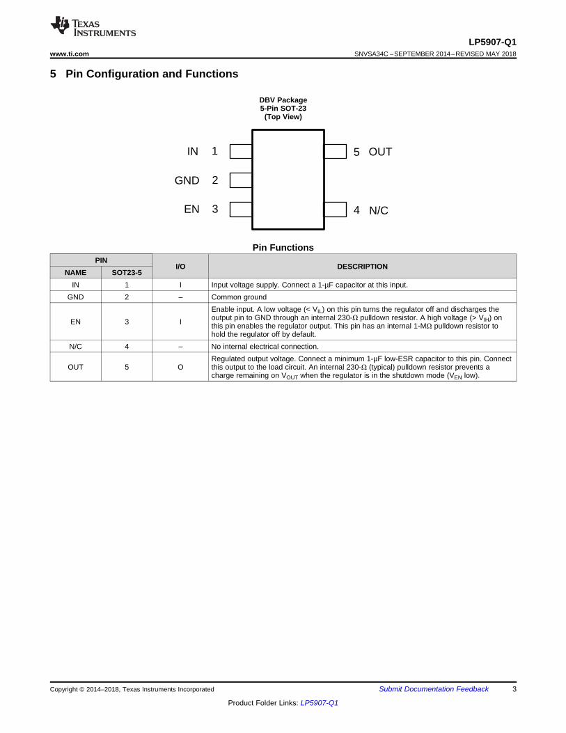
6 Specifications
6.1 Absolute Maximum Ratingsover operating free-air temperature range (unless otherwise noted) (1) (2)
MIN MAX UNITVIN Input voltage –0.3 6 VVOUT Output voltage –0.3 See (3) VVEN Enable input voltage –0.3 6 V
Continuous power dissipation (4) Internally limited WTJMAX Junction temperature 150 °CTstg Storage temperature –65 150 °C
(1) AEC Q100-002 indicates that HBM stressing shall be in accordance with the ANSI/ESDA/JEDEC JS-001 specification.
6.2 ESD RatingsVALUE UNIT
V(ESD) Electrostatic discharge
Human-body model (HBM), per AECQ100-002 (1) All pins ±2000
VCharged-device model (CDM), per AECQ100-011
Corner pins (1,3,4,5) ±1000Other pin (2) ±1000
(1) Stresses beyond those listed under Absolute Maximum Ratings may cause permanent damage to the device. These are stress ratingsonly, and functional operation of the device at these or any other conditions beyond those indicated under Recommended OperatingConditions is not implied. Exposure to absolute-maximum-rated conditions for extended periods may affect device reliability.
(2) All voltages are with respect to the GND pin.(3) TJ-MAX-OP = [TA(MAX) + (PD(MAX) × RθJA )].
6.3 Recommended Operating Conditionsover operating free-air temperature range (unless otherwise noted) (1) (2)
MIN MAX UNITVIN Input supply voltage 2.2 5.5 VVEN Enable input voltage 0 5.5 VIOUT Output current 0 250 mATJ-MAX-OP Operating junction temperature (3) –40 125 °C
(1) For more information about traditional and new thermal metrics, see the Semiconductor and IC Package Thermal Metrics applicationreport.
6.4 Thermal Information
THERMAL METRIC (1)LP5907-Q1
UNITDBV (SOT-23)5 PINS
RθJA Junction-to-ambient thermal resistance 186.9 °C/WRθJC(top) Junction-to-case (top) thermal resistance 112.3 °C/WRθJB Junction-to-board thermal resistance 52.3 °C/WψJT Junction-to-top characterization parameter 27.5 °C/WψJB Junction-to-board characterization parameter 51.8 °C/W
5
LP5907-Q1www.ti.com SNVSA34C –SEPTEMBER 2014–REVISED MAY 2018
Product Folder Links: LP5907-Q1
Submit Documentation FeedbackCopyright © 2014–2018, Texas Instruments Incorporated
(1) All voltages are with respect to the device GND terminal, unless otherwise stated.(2) Minimum and maximum limits are ensured through test, design, or statistical correlation over the junction temperature (TJ) range of
–40°C to 125°C, unless otherwise stated. Typical values represent the most likely parametric norm at TA = 25°C, and are provided forreference purposes only.
(3) In applications where high power dissipation and/or poor package thermal resistance is present, the maximum ambient temperature mayhave to be derated. Maximum ambient temperature (TA-MAX) is dependent on the maximum operating junction temperature (TJ-MAX-OP =125°C), the maximum power dissipation of the device in the application (PD-MAX), and the junction-to ambient thermal resistance of thepart/package in the application RθJA), as given by the following equation: TA-MAX = TJ-MAX-OP – (RθJA × PD-MAX). See Application andImplementation.
(4) Quiescent current is defined here as the difference in current between the input voltage source and the load at VOUT.(5) Ground current is defined here as the total current flowing to ground as a result of all input voltages applied to the device.(6) Dropout voltage is the voltage difference between the input and the output at which the output voltage drops to 100 mV below its
nominal value.(7) Short-circuit current (ISC) for the LP5907-Q1 is equivalent to current limit. To minimize thermal effects during testing, ISC is measured
with VOUT pulled to 100 mV below its nominal voltage.(8) This specification is verified by design.(9) There is a 1-MΩ resistor between EN and ground on the device.
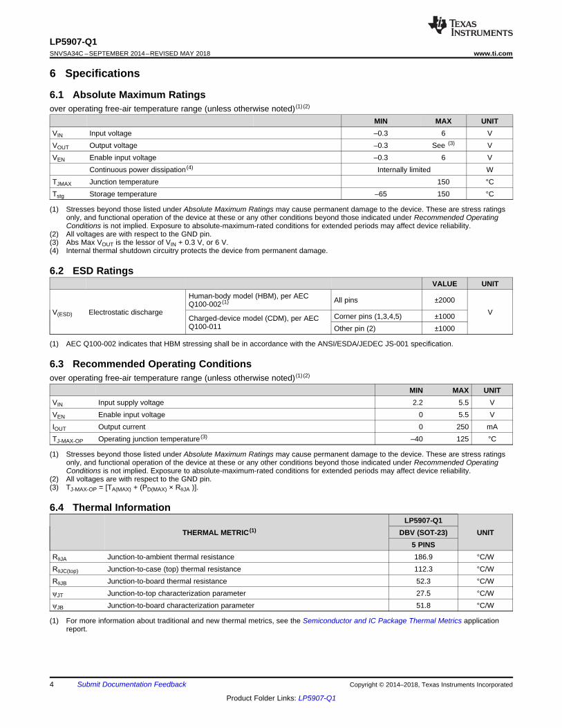
6.5 Electrical CharacteristicsVIN = VOUT(NOM) + 1 V, VEN = 1.2 V, IOUT = 1 mA, CIN = 1 µF, COUT = 1 µF (unless otherwise noted) (1) (2) (3)
PARAMETER TEST CONDITIONS MIN TYP MAX UNITGENERALVIN Input voltage TA = 25°C 2.2 5.5 V
ΔVOUT
Output voltage tolerance
VIN = (VOUT(NOM) + 1 V) to 5.5 V,IOUT = 1 mA to 250 mA, VOUT ≥ 1.8 V –2 2
%VOUTVIN = (VOUT(NOM) + 1 V) to 5.5 V,IOUT = 1 mA to 250 mA, VOUT < 1.8 V –3 3
Line regulation VIN = (VOUT(NOM) + 1 V) to 5.5 V,IOUT = 1 mA 0.02 %/V
Load regulation IOUT = 1 mA to 250 mA 0.001 %/mAILOAD Output load current 0 250 mA
IQ Quiescent current (4)
VEN = 1.2 V, IOUT = 0 mA 12 25µAVEN = 1.2 V, IOUT = 250 mA 250 425
VEN = 0.3 V (Disabled) 0.2 1IG Ground current (5) VEN = 1.2 V, IOUT = 0 mA 14 µA
VDO Dropout voltage (6) IOUT = 100 mA 50mV
IOUT = 250 mA 250ISC Short-circuit current limit TA = 25°C (7) 250 500 mA
PSRR Power-supply rejection ratio (8)
f = 100 Hz, IOUT = 20 mA 90
dBf = 1 kHz, IOUT = 20 mA 82f = 10 kHz, IOUT = 20 mA 65f = 100 kHz, IOUT = 20 mA 60
eN Output noise voltage (8) BW = 10 Hz to 100 kHzIOUT = 1 mA 10
µVRMSIOUT = 250 mA 6.5
RADOutput automatic dischargepulldown resistance VEN < VIL (output disabled) 230 Ω
TSDThermal shutdown TJ rising 160
°CThermal hysteresis TJ falling from shutdown 15
LOGIC INPUT THRESHOLDS
VIL Low input threshold VIN = 2.2 V to 5.5 V,VEN falling until the output is disabled 0.4 V
VIH High input threshold VIN = 2.2 V to 5.5 V,VEN rising until the output is enabled 1.2 V
IEN Input current at EN pin (9) VEN = 5.5 V and VIN = 5.5 V 5.5µA
VEN = 0 V and VIN = 5.5 V 0.001
6
LP5907-Q1SNVSA34C –SEPTEMBER 2014–REVISED MAY 2018 www.ti.com
Product Folder Links: LP5907-Q1
Submit Documentation Feedback Copyright © 2014–2018, Texas Instruments Incorporated
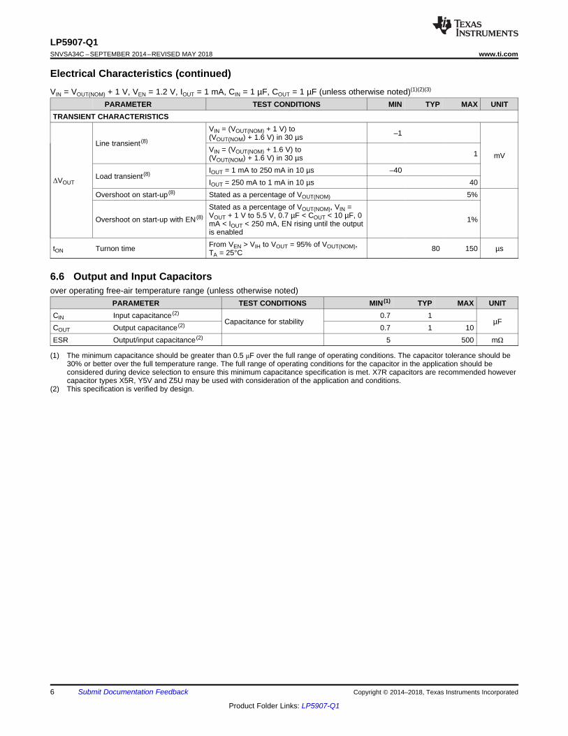
Electrical Characteristics (continued)VIN = VOUT(NOM) + 1 V, VEN = 1.2 V, IOUT = 1 mA, CIN = 1 µF, COUT = 1 µF (unless otherwise noted)(1)(2)(3)
PARAMETER TEST CONDITIONS MIN TYP MAX UNITTRANSIENT CHARACTERISTICS
ΔVOUT
Line transient (8)
VIN = (VOUT(NOM) + 1 V) to(VOUT(NOM) + 1.6 V) in 30 µs –1
mVVIN = (VOUT(NOM) + 1.6 V) to(VOUT(NOM) + 1.6 V) in 30 µs 1
Load transient (8) IOUT = 1 mA to 250 mA in 10 µs –40IOUT = 250 mA to 1 mA in 10 µs 40
Overshoot on start-up (8) Stated as a percentage of VOUT(NOM) 5%
Overshoot on start-up with EN (8)
Stated as a percentage of VOUT(NOM), VIN =VOUT + 1 V to 5.5 V, 0.7 µF < COUT < 10 µF, 0mA < IOUT < 250 mA, EN rising until the outputis enabled
1%
tON Turnon time From VEN > VIH to VOUT = 95% of VOUT(NOM),TA = 25°C 80 150 µs
(1) The minimum capacitance should be greater than 0.5 μF over the full range of operating conditions. The capacitor tolerance should be30% or better over the full temperature range. The full range of operating conditions for the capacitor in the application should beconsidered during device selection to ensure this minimum capacitance specification is met. X7R capacitors are recommended howevercapacitor types X5R, Y5V and Z5U may be used with consideration of the application and conditions.
(2) This specification is verified by design.
6.6 Output and Input Capacitorsover operating free-air temperature range (unless otherwise noted)
PARAMETER TEST CONDITIONS MIN (1) TYP MAX UNITCIN Input capacitance (2)
Capacitance for stability0.7 1
µFCOUT Output capacitance (2) 0.7 1 10ESR Output/input capacitance (2) 5 500 mΩ
0 50 100 150 200 250 300
0
50
100
150
200
250
300
350
GR
OU
ND
CU
RR
EN
T (�
A)
IOUT(mA)
VIN = 3.0VVIN = 3.8VVIN = 4.2VVIN = 5.5V
SVA-30180571
0 50 100 150 200 250
2.700
2.725
2.750
2.775
2.800
2.825
2.850
2.875
2.900
VO
UT
(V)
LOAD (mA)
VIN= 3.6V
-40°C90°C25°C
SVA-30180567
VIN (V)
VO
UT
(V
)
0 0.5 1 1.5 2 2.50
0.2
0.4
0.6
0.8
1
1.2
1.4
D002
RLOAD = 1.2 k:RLOAD = 4.8 :
VIN (V)
VO
UT
(V
)
0 1 2 3 4 5 60
0.5
1
1.5
2
2.5
3
3.5
4
4.5
5
D003
RLOAD = 4.5 k:RLOAD = 18 :
2.3 2.8 3.3 3.8 4.3 4.8 5.3 5.8
0
2
4
6
8
10
12
14
16
I Q(�
A)
VIN(V)SVA-30180569
VIN (V)
VE
N (
V)
2 2.5 3 3.5 4 4.5 5 5.5 60.5
0.6
0.7
0.8
0.9
1
D001
VIH RisingVIL Falling
7
LP5907-Q1www.ti.com SNVSA34C –SEPTEMBER 2014–REVISED MAY 2018
Product Folder Links: LP5907-Q1
Submit Documentation FeedbackCopyright © 2014–2018, Texas Instruments Incorporated
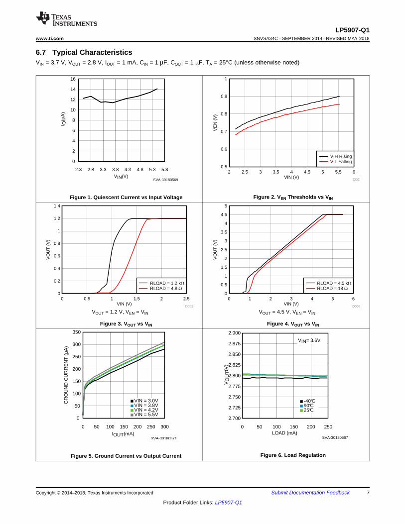
6.7 Typical CharacteristicsVIN = 3.7 V, VOUT = 2.8 V, IOUT = 1 mA, CIN = 1 µF, COUT = 1 µF, TA = 25°C (unless otherwise noted)
Figure 1. Quiescent Current vs Input Voltage Figure 2. VEN Thresholds vs VIN
VOUT = 1.2 V, VEN = VIN
Figure 3. VOUT vs VIN
VOUT = 4.5 V, VEN = VIN
Figure 4. VOUT vs VIN
Figure 5. Ground Current vs Output Current Figure 6. Load Regulation
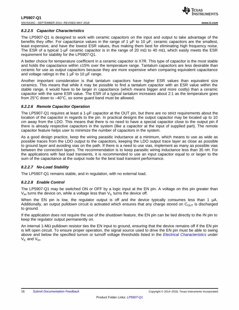
100 �s/DIV
VOUT 100 mV/DIV
LOAD 200 mA/DIV
SVA-30180512
100 �s/DIV
VOUT 100 mV/DIV
LOAD 200 mA/DIV
SVA-30180513
10 �s/DIV
VOUT (AC Coupled)
10 mV/DIV
1V/DIVVIN
SVA-30180510
10 �s/DIV
10 mV/DIV
1V/DIVVIN
VOUT (AC Coupled)
SVA-30180511
2 ms/DIV
VOUT
2V/DIV
2V/DIV
1A/DIV
VIN = VEN
IIN
SVA-30180509
3.0 3.5 4.0 4.5 5.0 5.5
2.700
2.725
2.750
2.775
2.800
2.825
2.850
2.875
2.900
VO
UT
(V)
VIN(V)
Load = 10 mA
-40°C90°C25°C
SVA-30180568
8
LP5907-Q1SNVSA34C –SEPTEMBER 2014–REVISED MAY 2018 www.ti.com
Product Folder Links: LP5907-Q1
Submit Documentation Feedback Copyright © 2014–2018, Texas Instruments Incorporated
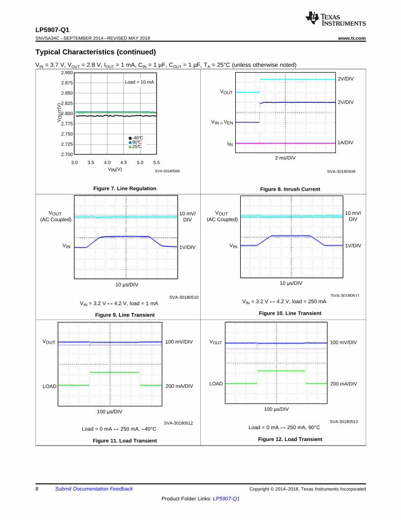
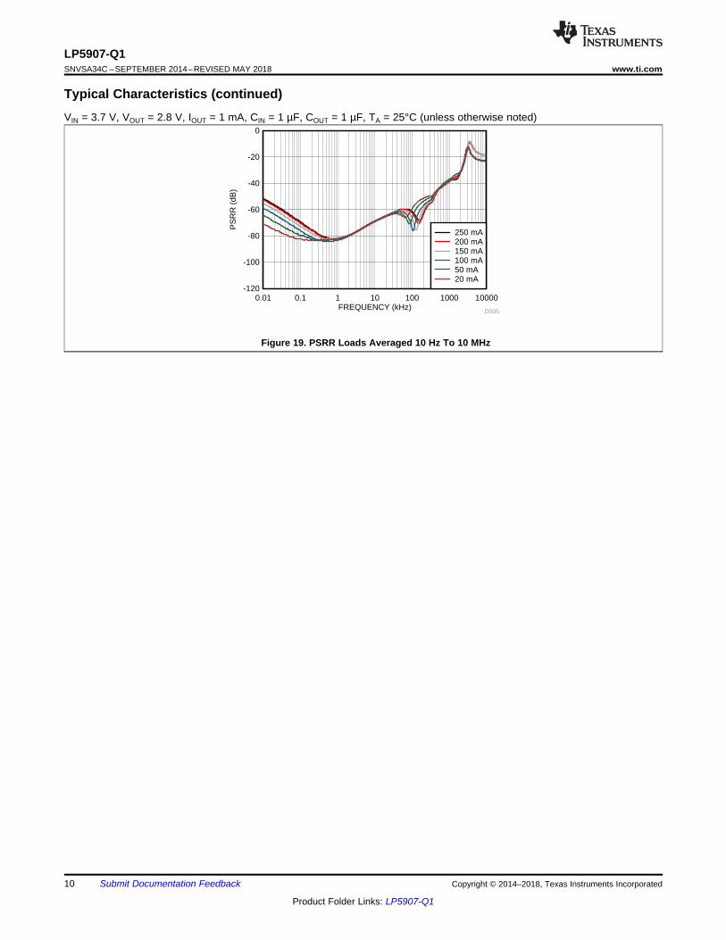
Typical Characteristics (continued)VIN = 3.7 V, VOUT = 2.8 V, IOUT = 1 mA, CIN = 1 µF, COUT = 1 µF, TA = 25°C (unless otherwise noted)
Figure 7. Line Regulation Figure 8. Inrush Current
VIN = 3.2 V ↔ 4.2 V, load = 1 mA
Figure 9. Line Transient
VIN = 3.2 V ↔ 4.2 V, load = 250 mA
Figure 10. Line Transient
Load = 0 mA ↔ 250 mA, –40°C
Figure 11. Load Transient
Load = 0 mA ↔ 250 mA, 90°C
Figure 12. Load Transient
FREQUENCY (kHz)
PS
RR
(dB
)
0.1 1 10 100-120
-100
-80
-60
-40
-20
0
D004
250 mA200 mA150 mA100 mA50 mA20 mA
0 50 100 150 200 250
0
20
40
60
80
100
120
140
DR
OP
OU
T V
OLT
AG
E (
mV
)
LOAD CURRENT (mA)
Dropout Voltage
SVA-30180573
20 �s/DIV
VOUT
1V/DIV
EN
1V/DIV
SVA-30180516
100 �s/DIV
VOUT 100 mV/DIV
LOAD 200 mA/DIV
SVA-30180514
20 �s/DIV
VOUT
1V/DIV
EN
1V/DIV
SVA-30180515
9
LP5907-Q1www.ti.com SNVSA34C –SEPTEMBER 2014–REVISED MAY 2018
Product Folder Links: LP5907-Q1
Submit Documentation FeedbackCopyright © 2014–2018, Texas Instruments Incorporated
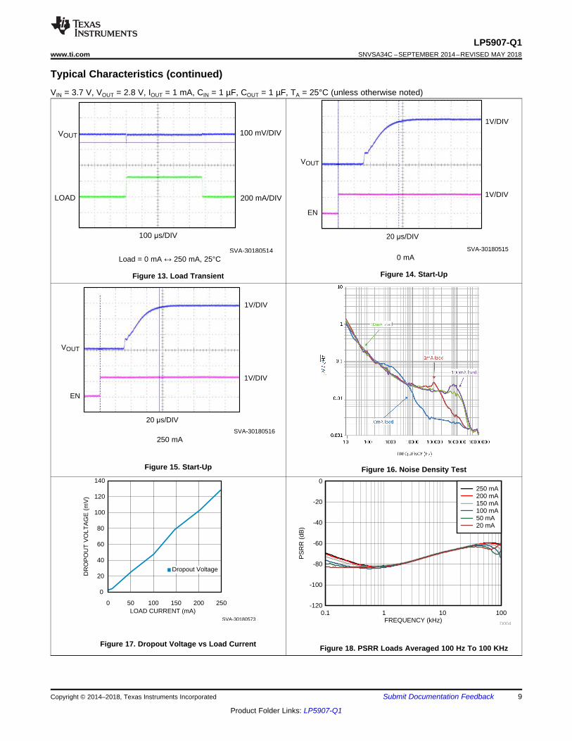
Typical Characteristics (continued)VIN = 3.7 V, VOUT = 2.8 V, IOUT = 1 mA, CIN = 1 µF, COUT = 1 µF, TA = 25°C (unless otherwise noted)
Load = 0 mA ↔ 250 mA, 25°C
Figure 13. Load Transient
0 mA
Figure 14. Start-Up
250 mA
Figure 15. Start-Up Figure 16. Noise Density Test
Figure 17. Dropout Voltage vs Load Current Figure 18. PSRR Loads Averaged 100 Hz To 100 KHz
FREQUENCY (kHz)
PS
RR
(dB
)
0.01 0.1 1 10 100 1000 10000-120
-100
-80
-60
-40
-20
0
D005
250 mA200 mA150 mA100 mA50 mA20 mA
10
LP5907-Q1SNVSA34C –SEPTEMBER 2014–REVISED MAY 2018 www.ti.com
Product Folder Links: LP5907-Q1
Submit Documentation Feedback Copyright © 2014–2018, Texas Instruments Incorporated
Typical Characteristics (continued)VIN = 3.7 V, VOUT = 2.8 V, IOUT = 1 mA, CIN = 1 µF, COUT = 1 µF, TA = 25°C (unless otherwise noted)
Figure 19. PSRR Loads Averaged 10 Hz To 10 MHz
IN
VBG1.20V
EN
+ ENEN
GND
POR
+
OUT
1 M VIH
RFCF
+
EN
EN
RAD
11
LP5907-Q1www.ti.com SNVSA34C –SEPTEMBER 2014–REVISED MAY 2018
Product Folder Links: LP5907-Q1
Submit Documentation FeedbackCopyright © 2014–2018, Texas Instruments Incorporated
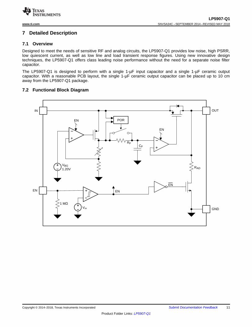
7 Detailed Description
7.1 OverviewDesigned to meet the needs of sensitive RF and analog circuits, the LP5907-Q1 provides low noise, high PSRR,low quiescent current, as well as low line and load transient response figures. Using new innovative designtechniques, the LP5907-Q1 offers class leading noise performance without the need for a separate noise filtercapacitor.
The LP5907-Q1 is designed to perform with a single 1-µF input capacitor and a single 1-µF ceramic outputcapacitor. With a reasonable PCB layout, the single 1-µF ceramic output capacitor can be placed up to 10 cmaway from the LP5907-Q1 package.
7.2 Functional Block Diagram
12
LP5907-Q1SNVSA34C –SEPTEMBER 2014–REVISED MAY 2018 www.ti.com
Product Folder Links: LP5907-Q1
Submit Documentation Feedback Copyright © 2014–2018, Texas Instruments Incorporated
7.3 Feature Description
7.3.1 LP5907-Q1 Voltage OptionsTable 1 lists the available voltage options for the LP5907-Q1 SOT-23 package.
Table 1. Voltage OptionsSOT-23 PACKAGE ORDER NUMBER VOLTAGE OPTION (V)
LP5907QMFX-1.2Q1 1.2— 1.3— 1.5
LP5907QMFX-1.8Q1 1.8LP5907QMFX-2.5Q1 2.5LP5907QMFX-2.8Q1 2.8
2.852.9
LP5907QMFX-3.0Q1 3.0LP5907QMFX-3.3Q1 3.3LP5907QMFX-3.8Q1 3.8LP5907QMFX-4.5Q1 4.5
7.3.2 Enable (EN)The LP5907-Q1 EN pin is internally held low by a 1-MΩ resistor to GND. The EN pin voltage must be higher thanthe VIH threshold to ensure that the device is fully enabled under all operating conditions. The EN pin voltagemust be lower than the VIL threshold to ensure that the device is fully disabled and the automatic outputdischarge is activated.
7.3.3 Low Output NoiseAny internal noise at the LP5907-Q1 reference voltage is reduced by a first order low-pass RC filter before it ispassed to the output buffer stage. The low-pass RC filter has a –3 dB cut-off frequency of approximately 0.1 Hz.
7.3.4 Output Automatic DischargeThe LP5907-Q1 output employs an internal 230-Ω (typical) pulldown resistance to discharge the output when theEN pin is low, and the device is disabled.
7.3.5 Remote Output Capacitor PlacementThe LP5907-Q1 requires at least a 1-µF capacitor at the OUT pin, but there are no strict requirements about thelocation of the capacitor in regards the OUT pin. In practical designs, the output capacitor may be located up to10 cm away from the LDO.
7.3.6 Thermal Overload Protection (TSD)Thermal shutdown disables the output when the junction temperature rises to approximately 160°C which allowsthe device to cool. When the junction temperature cools to approximately 145°C, the output circuitry enables.Based on power dissipation, thermal resistance, and ambient temperature, the thermal protection circuit maycycle on and off. This thermal cycling limits the dissipation of the regulator and protects it from damage as aresult of overheating.
The thermal shutdown circuitry of the LP5907-Q1 has been designed to protect against temporary thermaloverload conditions. The thermal shutdown circuitry was not intended to replace proper heat-sinking.Continuously running the LP5907-Q1 device into thermal shutdown may degrade device reliability.
13
LP5907-Q1www.ti.com SNVSA34C –SEPTEMBER 2014–REVISED MAY 2018
Product Folder Links: LP5907-Q1
Submit Documentation FeedbackCopyright © 2014–2018, Texas Instruments Incorporated
7.4 Device Functional Modes
7.4.1 Enable (EN)The LP5907-Q1 Enable (EN) pin is internally held low by a 1-MΩ resistor to GND. The EN pin voltage must behigher than the VIH threshold to ensure that the device is fully enabled under all operating conditions.
When the EN pin is pulled low, and the output is disabled, the output automatic discharge circuitry is activated.Any charge on the OUT pin is discharged to GND through the internal 230-Ω (typical) pull-down resistance.
7.4.2 Minimum Operating Input Voltage (VIN)The LP5907-Q1 does not include any dedicated undervoltage lockout circuitry. The LP5907-Q1 internal circuitryis not fully functional until VIN is at least 2.2 V. The output voltage is not regulated until VIN has reached at leastthe greater of 2.2 V or (VOUT + VDO).
EN
IN OUT
GND
1 PF 1 PF
INPUT
ENABLE
GND
OUTPUT
LP5907-Q1
14
LP5907-Q1SNVSA34C –SEPTEMBER 2014–REVISED MAY 2018 www.ti.com
Product Folder Links: LP5907-Q1
Submit Documentation Feedback Copyright © 2014–2018, Texas Instruments Incorporated
8 Application and Implementation
NOTEInformation in the following applications sections is not part of the TI componentspecification, and TI does not warrant its accuracy or completeness. TI’s customers areresponsible for determining suitability of components for their purposes. Customers shouldvalidate and test their design implementation to confirm system functionality.
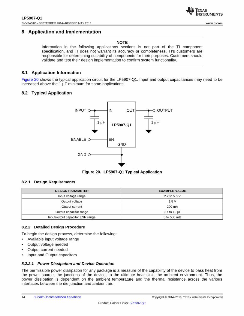
8.1 Application InformationFigure 20 shows the typical application circuit for the LP5907-Q1. Input and output capacitances may need to beincreased above the 1 µF minimum for some applications.
8.2 Typical Application
Figure 20. LP5907-Q1 Typical Application
8.2.1 Design Requirements
DESIGN PARAMETER EXAMPLE VALUEInput voltage range 2.2 to 5.5 V
Output voltage 1.8 VOutput current 200 mA
Output capacitor range 0.7 to 10 µFInput/output capacitor ESR range 5 to 500 mΩ
8.2.2 Detailed Design ProcedureTo begin the design process, determine the following:• Available input voltage range• Output voltage needed• Output current needed• Input and Output capacitors
8.2.2.1 Power Dissipation and Device OperationThe permissible power dissipation for any package is a measure of the capability of the device to pass heat fromthe power source, the junctions of the device, to the ultimate heat sink, the ambient environment. Thus, thepower dissipation is dependent on the ambient temperature and the thermal resistance across the variousinterfaces between the die junction and ambient air.
15
LP5907-Q1www.ti.com SNVSA34C –SEPTEMBER 2014–REVISED MAY 2018
Product Folder Links: LP5907-Q1
Submit Documentation FeedbackCopyright © 2014–2018, Texas Instruments Incorporated
The maximum allowable power dissipation for the device in a given package can be calculated using Equation 1:PD-MAX = ((TJ-MAX – TA) / RθJA) (1)
The actual power being dissipated in the device can be represented by Equation 2:PD = (VIN - VOUT) × IOUT (2)
Equation 1 and Equation 2 establish the relationship between the maximum power dissipation allowed due tothermal consideration, the voltage drop across the device, and the continuous current capability of the device.These two equations should be used to determine the optimum operating conditions for the device in theapplication.
In applications where lower power dissipation (PD) and/or excellent package thermal resistance (RθJA) is present,the maximum ambient temperature (TA-MAX) may be increased.
In applications where high power dissipation and/or poor package thermal resistance is present, the maximumambient temperature (TA-MAX) may have to be derated. TA-MAX is dependent on the maximum operating junctiontemperature (TJ-MAX-OP = 125°C), the maximum allowable power dissipation in the device package in theapplication (PD-MAX), and the junction-to ambient thermal resistance of the part/package in the application (RθJA),as given by Equation 3:
TA-MAX = (TJ-MAX-OP – (RθJA × PD-MAX)) (3)
Alternately, if TA-MAX can not be derated, the PD value must be reduced. This can be accomplished by reducingVIN in the VIN – VOUT term as long as the minimum VIN is met, or by reducing the IOUT term, or by somecombination of the two.
8.2.2.2 External CapacitorsLike most LDOs, the LP5907-Q1 requires external capacitors for regulator stability. The device is specificallydesigned for portable applications requiring minimum board space and smallest components. These capacitorsmust be correctly selected for good performance.
8.2.2.3 Input CapacitorAn input capacitor is required for stability. The input capacitor should be at least equal to, or greater than, theoutput capacitor for good load transient performance. At least a 1-µF capacitor has to be connected between theLP5907-Q1 input pin and ground for stable operation over full load current range. Basically, it is acceptable tohave more output capacitance than input, as long as the input is at least 1 µF.
The input capacitor must be located a distance of not more than 1 cm from the IN pin and returned to a cleananalog ground. Any good quality ceramic, tantalum, or film capacitor may be used at the input.
Important: To ensure stable operation it is essential that good PCB practices are employed to minimize groundimpedance and keep input inductance low. If these conditions cannot be met, or if long leads are to be used toconnect the battery or other power source to the LP5907-Q1, TI recommends increasing the input capacitor to atleast 10 µF. Also, tantalum capacitors can suffer catastrophic failures due to surge current when connected to alow-impedance source of power (like a battery or a very large capacitor). If a tantalum capacitor is used at theinput, it must be verified by the manufacturer to have a surge current rating sufficient for the application. Theinitial tolerance, applied voltage de-rating, and temperature coefficient must all be considered when selecting theinput capacitor to ensure the actual capacitance is never less than 0.7 µF over the entire operating range.
8.2.2.4 Output CapacitorThe LP5907-Q1 is designed specifically to work with a very small ceramic output capacitor, typically 1 µF. Aceramic capacitor (dielectric types X5R or X7R) in the 1-µF to 10-µF range, and with equivalent series resistance(ESR) between 5 mΩ to 500 mΩ, is suitable in the LP5907-Q1 application circuit. For this device connect theoutput capacitor between the OUT pin and a good connection back to the GND pin.
It may also be possible to use tantalum or film capacitors at the device output, VOUT, but these are not asattractive for reasons of size and cost (see Capacitor Characteristics).
The output capacitor must meet the requirement for the minimum value of capacitance and have an ESR valuethat is within the range 5 mΩ to 500 mΩ for stability. Like the input capacitor, the initial tolerance, applied voltagede-rating, and temperature coefficient must all be considered when selecting the input capacitor to ensure theactual capacitance is never less than 0.7 µF over the entire operating range.
16
LP5907-Q1SNVSA34C –SEPTEMBER 2014–REVISED MAY 2018 www.ti.com
Product Folder Links: LP5907-Q1
Submit Documentation Feedback Copyright © 2014–2018, Texas Instruments Incorporated
8.2.2.5 Capacitor CharacteristicsThe LP5907-Q1 is designed to work with ceramic capacitors on the input and output to take advantage of thebenefits they offer. For capacitance values in the range of 1 µF to 10 µF, ceramic capacitors are the smallest,least expensive, and have the lowest ESR values, thus making them best for eliminating high frequency noise.The ESR of a typical 1-µF ceramic capacitor is in the range of 20 mΩ to 40 mΩ, which easily meets the ESRrequirement for stability for the LP5907-Q1.
A better choice for temperature coefficient in a ceramic capacitor is X7R. This type of capacitor is the most stableand holds the capacitance within ±15% over the temperature range. Tantalum capacitors are less desirable thanceramic for use as output capacitors because they are more expensive when comparing equivalent capacitanceand voltage ratings in the 1 µF to 10 µF range.
Another important consideration is that tantalum capacitors have higher ESR values than equivalent sizeceramics. This means that while it may be possible to find a tantalum capacitor with an ESR value within thestable range, it would have to be larger in capacitance (which means bigger and more costly) than a ceramiccapacitor with the same ESR value. The ESR of a typical tantalum increases about 2:1 as the temperature goesfrom 25°C down to –40°C, so some guard band must be allowed.
8.2.2.6 Remote Capacitor OperationThe LP5907-Q1 requires at least a 1-µF capacitor at the OUT pin, but there are no strict requirements about thelocation of the capacitor in regards to the pin. In practical designs the output capacitor may be located up to 10cm away from the LDO. This means that there is no need to have a special capacitor close to the output pin ifthere is already respective capacitors in the system (like a capacitor at the input of supplied part). The remotecapacitor feature helps user to minimize the number of capacitors in the system.
As a good design practice, keep the wiring parasitic inductance at a minimum, which means to use as wide aspossible traces from the LDO output to the capacitors, keeping the LDO output trace layer as close as possibleto ground layer and avoiding vias on the path. If there is a need to use vias, implement as many as possible viasbetween the connection layers. The recommendation is to keep parasitic wiring inductance less than 35 nH. Forthe applications with fast load transients, it is recommended to use an input capacitor equal to or larger to thesum of the capacitance at the output node for the best load transient performance.
8.2.2.7 No-Load StabilityThe LP5907-Q1 remains stable, and in regulation, with no external load.
8.2.2.8 Enable ControlThe LP5907-Q1 may be switched ON or OFF by a logic input at the EN pin. A voltage on this pin greater thanVIH turns the device on, while a voltage less than VIL turns the device off.
When the EN pin is low, the regulator output is off and the device typically consumes less than 1 µA.Additionally, an output pulldown circuit is activated which ensures that any charge stored on COUT is dischargedto ground.
If the application does not require the use of the shutdown feature, the EN pin can be tied directly to the IN pin tokeep the regulator output permanently on.
An internal 1-MΩ pulldown resistor ties the EN input to ground, ensuring that the device remains off if the EN pinis left open circuit. To ensure proper operation, the signal source used to drive the EN pin must be able to swingabove and below the specified turnon or turnoff voltage thresholds listed in the Electrical Characteristics underVIL and VIH.
IN
GND
EN
OUT
N/C
CIN COUT1
2
3 4
5
VIN
GND
Enable
VOUT
GND
20 �s/DIV
VOUT
1V/DIV
EN
1V/DIV
SVA-30180515
100 �s/DIV
VOUT 100 mV/DIV
LOAD 200 mA/DIV
SVA-30180514
17
LP5907-Q1www.ti.com SNVSA34C –SEPTEMBER 2014–REVISED MAY 2018
Product Folder Links: LP5907-Q1
Submit Documentation FeedbackCopyright © 2014–2018, Texas Instruments Incorporated
8.2.3 Application Curves
Figure 21. Start-Up Figure 22. Load Transient Response
9 Power Supply RecommendationsThis device is designed to operate from an input supply voltage range of 2.2 V to 5.5 V. The input supply mustbe well regulated and free of spurious noise. To ensure that the LP5907-Q1 output voltage is well regulated anddynamic performance is optimum, the input supply must be at least VOUT + 1 V. A minimum capacitor value of1 µF is required to be within 1 cm of the IN pin.
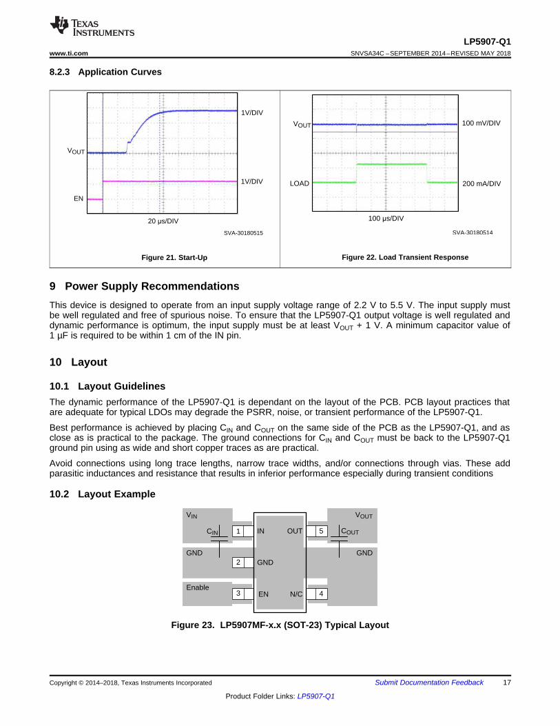
10 Layout
10.1 Layout GuidelinesThe dynamic performance of the LP5907-Q1 is dependant on the layout of the PCB. PCB layout practices thatare adequate for typical LDOs may degrade the PSRR, noise, or transient performance of the LP5907-Q1.
Best performance is achieved by placing CIN and COUT on the same side of the PCB as the LP5907-Q1, and asclose as is practical to the package. The ground connections for CIN and COUT must be back to the LP5907-Q1ground pin using as wide and short copper traces as are practical.
Avoid connections using long trace lengths, narrow trace widths, and/or connections through vias. These addparasitic inductances and resistance that results in inferior performance especially during transient conditions
10.2 Layout Example
Figure 23. LP5907MF-x.x (SOT-23) Typical Layout
18
LP5907-Q1SNVSA34C –SEPTEMBER 2014–REVISED MAY 2018 www.ti.com
Product Folder Links: LP5907-Q1
Submit Documentation Feedback Copyright © 2014–2018, Texas Instruments Incorporated
11 Device and Documentation Support
11.1 Receiving Notification of Documentation UpdatesTo receive notification of documentation updates, navigate to the device product folder on ti.com. In the upperright corner, click on Alert me to register and receive a weekly digest of any product information that haschanged. For change details, review the revision history included in any revised document.
11.2 Community ResourcesThe following links connect to TI community resources. Linked contents are provided "AS IS" by the respectivecontributors. They do not constitute TI specifications and do not necessarily reflect TI's views; see TI's Terms ofUse.
TI E2E™ Online Community TI's Engineer-to-Engineer (E2E) Community. Created to foster collaborationamong engineers. At e2e.ti.com, you can ask questions, share knowledge, explore ideas and helpsolve problems with fellow engineers.
Design Support TI's Design Support Quickly find helpful E2E forums along with design support tools andcontact information for technical support.
11.3 TrademarksE2E is a trademark of Texas Instruments.All other trademarks are the property of their respective owners.
11.4 Electrostatic Discharge CautionThese devices have limited built-in ESD protection. The leads should be shorted together or the device placed in conductive foamduring storage or handling to prevent electrostatic damage to the MOS gates.
11.5 GlossarySLYZ022 — TI Glossary.
This glossary lists and explains terms, acronyms, and definitions.
12 Mechanical, Packaging, and Orderable InformationThe following pages include mechanical, packaging, and orderable information. This information is the mostcurrent data available for the designated devices. This data is subject to change without notice and revision ofthis document. For browser-based versions of this data sheet, refer to the left-hand navigation.
PACKAGE OPTION ADDENDUM
www.ti.com 13-Mar-2018
Addendum-Page 1
PACKAGING INFORMATION
Orderable Device Status(1)
Package Type PackageDrawing
Pins PackageQty
Eco Plan(2)
Lead/Ball Finish(6)
MSL Peak Temp(3)
Op Temp (°C) Device Marking(4/5)
Samples
LP5907QMFX-1.2Q1 ACTIVE SOT-23 DBV 5 3000 Green (RoHS& no Sb/Br)
CU SN Level-1-260C-UNLIM -40 to 125 RAFQ
LP5907QMFX-1.8Q1 ACTIVE SOT-23 DBV 5 3000 Green (RoHS& no Sb/Br)
CU SN Level-1-260C-UNLIM -40 to 125 RAGQ
LP5907QMFX-2.5Q1 ACTIVE SOT-23 DBV 5 3000 Green (RoHS& no Sb/Br)
CU SN Level-1-260C-UNLIM -40 to 125 RAJQ
LP5907QMFX-2.8Q1 ACTIVE SOT-23 DBV 5 3000 Green (RoHS& no Sb/Br)
CU SN Level-1-260C-UNLIM -40 to 125 RAKQ
LP5907QMFX-3.0Q1 ACTIVE SOT-23 DBV 5 3000 Green (RoHS& no Sb/Br)
CU SN Level-1-260C-UNLIM -40 to 125 RALQ
LP5907QMFX-3.3Q1 ACTIVE SOT-23 DBV 5 3000 Green (RoHS& no Sb/Br)
CU SN Level-1-260C-UNLIM -40 to 125 RAHQ
LP5907QMFX-3.8Q1 ACTIVE SOT-23 DBV 5 3000 Green (RoHS& no Sb/Br)
CU SN Level-1-260C-UNLIM -40 to 125 RAMQ
LP5907QMFX-4.5Q1 ACTIVE SOT-23 DBV 5 3000 Green (RoHS& no Sb/Br)
CU SN Level-1-260C-UNLIM -40 to 125 RAIQ
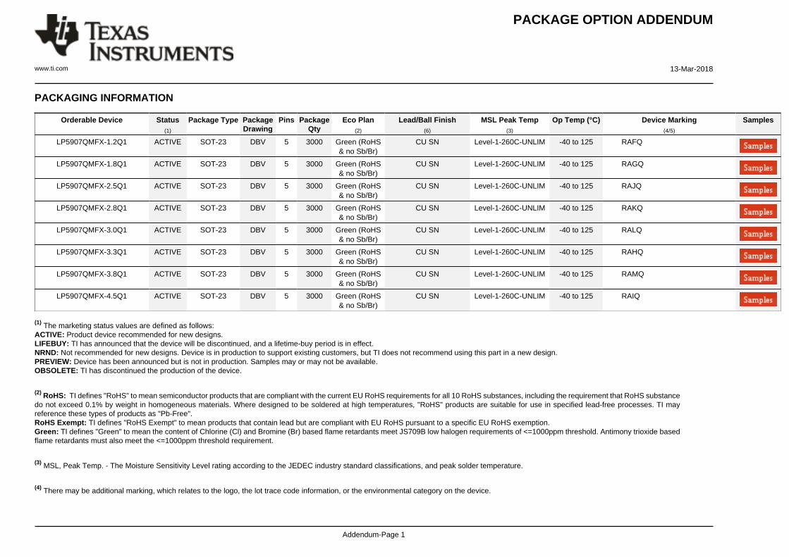
(1) The marketing status values are defined as follows:ACTIVE: Product device recommended for new designs.LIFEBUY: TI has announced that the device will be discontinued, and a lifetime-buy period is in effect.NRND: Not recommended for new designs. Device is in production to support existing customers, but TI does not recommend using this part in a new design.PREVIEW: Device has been announced but is not in production. Samples may or may not be available.OBSOLETE: TI has discontinued the production of the device.
(2) RoHS: TI defines "RoHS" to mean semiconductor products that are compliant with the current EU RoHS requirements for all 10 RoHS substances, including the requirement that RoHS substancedo not exceed 0.1% by weight in homogeneous materials. Where designed to be soldered at high temperatures, "RoHS" products are suitable for use in specified lead-free processes. TI mayreference these types of products as "Pb-Free".RoHS Exempt: TI defines "RoHS Exempt" to mean products that contain lead but are compliant with EU RoHS pursuant to a specific EU RoHS exemption.Green: TI defines "Green" to mean the content of Chlorine (Cl) and Bromine (Br) based flame retardants meet JS709B low halogen requirements of <=1000ppm threshold. Antimony trioxide basedflame retardants must also meet the <=1000ppm threshold requirement.
(3) MSL, Peak Temp. - The Moisture Sensitivity Level rating according to the JEDEC industry standard classifications, and peak solder temperature.
(4) There may be additional marking, which relates to the logo, the lot trace code information, or the environmental category on the device.
PACKAGE OPTION ADDENDUM
www.ti.com 13-Mar-2018
Addendum-Page 2
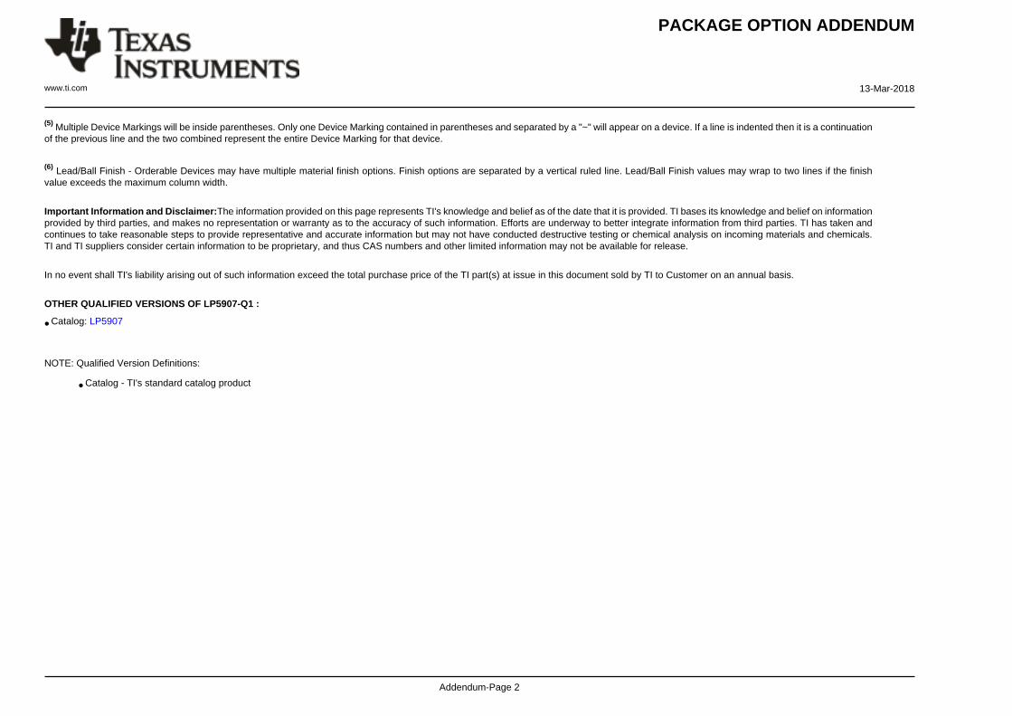
(5) Multiple Device Markings will be inside parentheses. Only one Device Marking contained in parentheses and separated by a "~" will appear on a device. If a line is indented then it is a continuationof the previous line and the two combined represent the entire Device Marking for that device.
(6) Lead/Ball Finish - Orderable Devices may have multiple material finish options. Finish options are separated by a vertical ruled line. Lead/Ball Finish values may wrap to two lines if the finishvalue exceeds the maximum column width.
Important Information and Disclaimer:The information provided on this page represents TI's knowledge and belief as of the date that it is provided. TI bases its knowledge and belief on informationprovided by third parties, and makes no representation or warranty as to the accuracy of such information. Efforts are underway to better integrate information from third parties. TI has taken andcontinues to take reasonable steps to provide representative and accurate information but may not have conducted destructive testing or chemical analysis on incoming materials and chemicals.TI and TI suppliers consider certain information to be proprietary, and thus CAS numbers and other limited information may not be available for release.
In no event shall TI's liability arising out of such information exceed the total purchase price of the TI part(s) at issue in this document sold by TI to Customer on an annual basis.
OTHER QUALIFIED VERSIONS OF LP5907-Q1 :
• Catalog: LP5907
NOTE: Qualified Version Definitions:
• Catalog - TI's standard catalog product
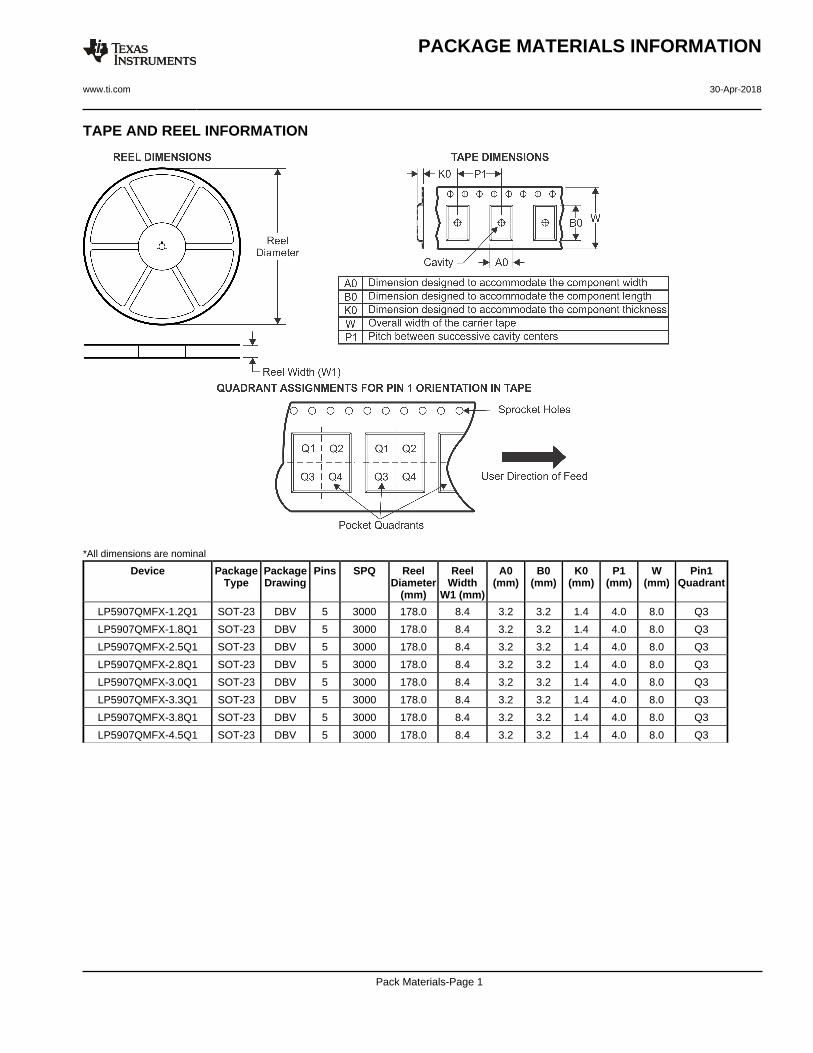
TAPE AND REEL INFORMATION
*All dimensions are nominal
Device PackageType
PackageDrawing
Pins SPQ ReelDiameter
(mm)
ReelWidth
W1 (mm)
A0(mm)
B0(mm)
K0(mm)
P1(mm)
W(mm)
Pin1Quadrant
LP5907QMFX-1.2Q1 SOT-23 DBV 5 3000 178.0 8.4 3.2 3.2 1.4 4.0 8.0 Q3
LP5907QMFX-1.8Q1 SOT-23 DBV 5 3000 178.0 8.4 3.2 3.2 1.4 4.0 8.0 Q3
LP5907QMFX-2.5Q1 SOT-23 DBV 5 3000 178.0 8.4 3.2 3.2 1.4 4.0 8.0 Q3
LP5907QMFX-2.8Q1 SOT-23 DBV 5 3000 178.0 8.4 3.2 3.2 1.4 4.0 8.0 Q3
LP5907QMFX-3.0Q1 SOT-23 DBV 5 3000 178.0 8.4 3.2 3.2 1.4 4.0 8.0 Q3
LP5907QMFX-3.3Q1 SOT-23 DBV 5 3000 178.0 8.4 3.2 3.2 1.4 4.0 8.0 Q3
LP5907QMFX-3.8Q1 SOT-23 DBV 5 3000 178.0 8.4 3.2 3.2 1.4 4.0 8.0 Q3
LP5907QMFX-4.5Q1 SOT-23 DBV 5 3000 178.0 8.4 3.2 3.2 1.4 4.0 8.0 Q3
PACKAGE MATERIALS INFORMATION
www.ti.com 30-Apr-2018
Pack Materials-Page 1
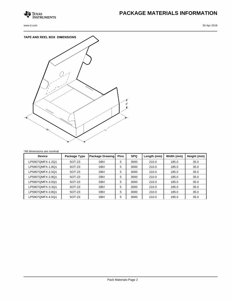
*All dimensions are nominal
Device Package Type Package Drawing Pins SPQ Length (mm) Width (mm) Height (mm)
LP5907QMFX-1.2Q1 SOT-23 DBV 5 3000 210.0 185.0 35.0
LP5907QMFX-1.8Q1 SOT-23 DBV 5 3000 210.0 185.0 35.0
LP5907QMFX-2.5Q1 SOT-23 DBV 5 3000 210.0 185.0 35.0
LP5907QMFX-2.8Q1 SOT-23 DBV 5 3000 210.0 185.0 35.0
LP5907QMFX-3.0Q1 SOT-23 DBV 5 3000 210.0 185.0 35.0
LP5907QMFX-3.3Q1 SOT-23 DBV 5 3000 210.0 185.0 35.0
LP5907QMFX-3.8Q1 SOT-23 DBV 5 3000 210.0 185.0 35.0
LP5907QMFX-4.5Q1 SOT-23 DBV 5 3000 210.0 185.0 35.0
PACKAGE MATERIALS INFORMATION
www.ti.com 30-Apr-2018
Pack Materials-Page 2
www.ti.com
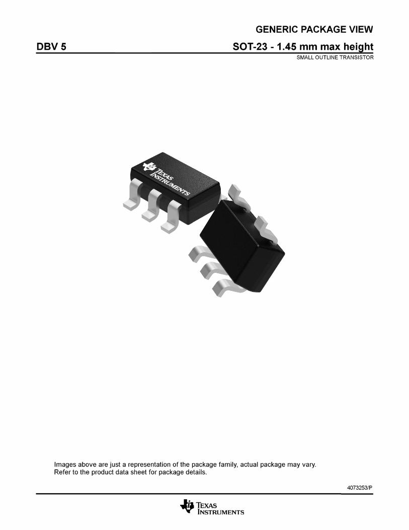
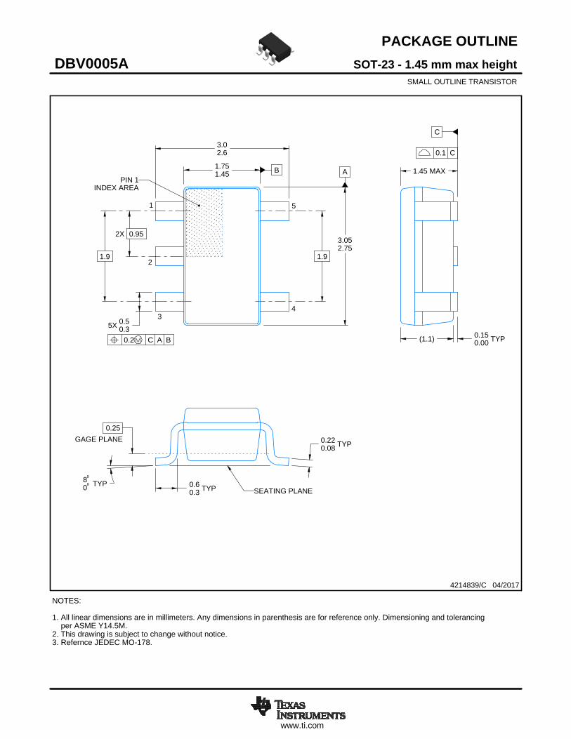
PACKAGE OUTLINE
C
TYP0.220.08
0.25
3.02.6
2X 0.95
1.9
1.45 MAX
TYP0.150.00
5X 0.50.3
TYP0.60.3
TYP80
1.9
A
3.052.75
B1.751.45
(1.1)
SOT-23 - 1.45 mm max heightDBV0005ASMALL OUTLINE TRANSISTOR
4214839/C 04/2017
NOTES: 1. All linear dimensions are in millimeters. Any dimensions in parenthesis are for reference only. Dimensioning and tolerancing per ASME Y14.5M.2. This drawing is subject to change without notice.3. Refernce JEDEC MO-178.
0.2 C A B
1
34
5
2
INDEX AREAPIN 1
GAGE PLANE
SEATING PLANE
0.1 C
SCALE 4.000
www.ti.com
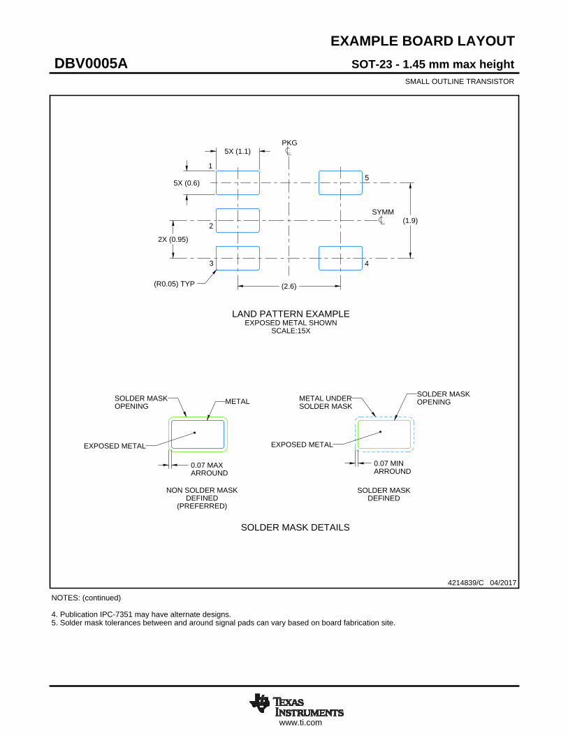
EXAMPLE BOARD LAYOUT
0.07 MAXARROUND
0.07 MINARROUND
5X (1.1)
5X (0.6)
(2.6)
(1.9)
2X (0.95)
(R0.05) TYP
4214839/C 04/2017
SOT-23 - 1.45 mm max heightDBV0005ASMALL OUTLINE TRANSISTOR
NOTES: (continued) 4. Publication IPC-7351 may have alternate designs. 5. Solder mask tolerances between and around signal pads can vary based on board fabrication site.
SYMM
LAND PATTERN EXAMPLEEXPOSED METAL SHOWN
SCALE:15X
PKG
1
3 4
5
2
SOLDER MASKOPENINGMETAL UNDER
SOLDER MASK
SOLDER MASKDEFINED
EXPOSED METAL
METALSOLDER MASKOPENING
NON SOLDER MASKDEFINED
(PREFERRED)
SOLDER MASK DETAILS
EXPOSED METAL
www.ti.com
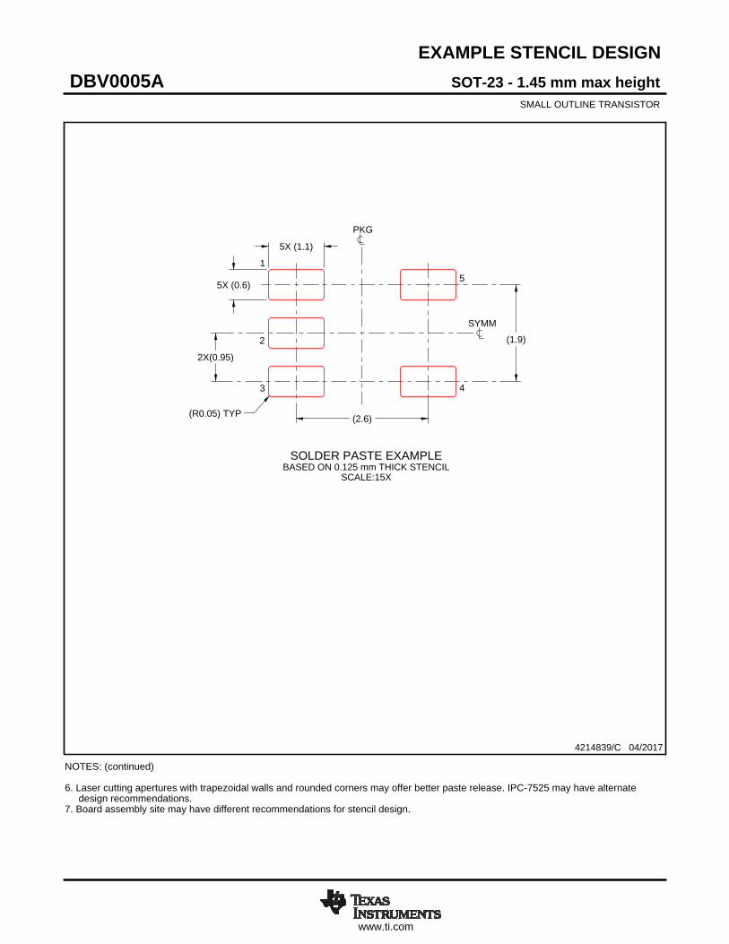
EXAMPLE STENCIL DESIGN
(2.6)
(1.9)
2X(0.95)
5X (1.1)
5X (0.6)
(R0.05) TYP
SOT-23 - 1.45 mm max heightDBV0005ASMALL OUTLINE TRANSISTOR
4214839/C 04/2017
NOTES: (continued) 6. Laser cutting apertures with trapezoidal walls and rounded corners may offer better paste release. IPC-7525 may have alternate design recommendations. 7. Board assembly site may have different recommendations for stencil design.
SOLDER PASTE EXAMPLEBASED ON 0.125 mm THICK STENCIL
SCALE:15X
SYMM
PKG
1
3 4
5
2
IMPORTANT NOTICE
Texas Instruments Incorporated (TI) reserves the right to make corrections, enhancements, improvements and other changes to itssemiconductor products and services per JESD46, latest issue, and to discontinue any product or service per JESD48, latest issue. Buyersshould obtain the latest relevant information before placing orders and should verify that such information is current and complete.TI’s published terms of sale for semiconductor products (http://www.ti.com/sc/docs/stdterms.htm) apply to the sale of packaged integratedcircuit products that TI has qualified and released to market. Additional terms may apply to the use or sale of other types of TI products andservices.Reproduction of significant portions of TI information in TI data sheets is permissible only if reproduction is without alteration and isaccompanied by all associated warranties, conditions, limitations, and notices. TI is not responsible or liable for such reproduceddocumentation. Information of third parties may be subject to additional restrictions. Resale of TI products or services with statementsdifferent from or beyond the parameters stated by TI for that product or service voids all express and any implied warranties for theassociated TI product or service and is an unfair and deceptive business practice. TI is not responsible or liable for any such statements.Buyers and others who are developing systems that incorporate TI products (collectively, “Designers”) understand and agree that Designersremain responsible for using their independent analysis, evaluation and judgment in designing their applications and that Designers havefull and exclusive responsibility to assure the safety of Designers' applications and compliance of their applications (and of all TI productsused in or for Designers’ applications) with all applicable regulations, laws and other applicable requirements. Designer represents that, withrespect to their applications, Designer has all the necessary expertise to create and implement safeguards that (1) anticipate dangerousconsequences of failures, (2) monitor failures and their consequences, and (3) lessen the likelihood of failures that might cause harm andtake appropriate actions. Designer agrees that prior to using or distributing any applications that include TI products, Designer willthoroughly test such applications and the functionality of such TI products as used in such applications.TI’s provision of technical, application or other design advice, quality characterization, reliability data or other services or information,including, but not limited to, reference designs and materials relating to evaluation modules, (collectively, “TI Resources”) are intended toassist designers who are developing applications that incorporate TI products; by downloading, accessing or using TI Resources in anyway, Designer (individually or, if Designer is acting on behalf of a company, Designer’s company) agrees to use any particular TI Resourcesolely for this purpose and subject to the terms of this Notice.TI’s provision of TI Resources does not expand or otherwise alter TI’s applicable published warranties or warranty disclaimers for TIproducts, and no additional obligations or liabilities arise from TI providing such TI Resources. TI reserves the right to make corrections,enhancements, improvements and other changes to its TI Resources. TI has not conducted any testing other than that specificallydescribed in the published documentation for a particular TI Resource.Designer is authorized to use, copy and modify any individual TI Resource only in connection with the development of applications thatinclude the TI product(s) identified in such TI Resource. NO OTHER LICENSE, EXPRESS OR IMPLIED, BY ESTOPPEL OR OTHERWISETO ANY OTHER TI INTELLECTUAL PROPERTY RIGHT, AND NO LICENSE TO ANY TECHNOLOGY OR INTELLECTUAL PROPERTYRIGHT OF TI OR ANY THIRD PARTY IS GRANTED HEREIN, including but not limited to any patent right, copyright, mask work right, orother intellectual property right relating to any combination, machine, or process in which TI products or services are used. Informationregarding or referencing third-party products or services does not constitute a license to use such products or services, or a warranty orendorsement thereof. Use of TI Resources may require a license from a third party under the patents or other intellectual property of thethird party, or a license from TI under the patents or other intellectual property of TI.TI RESOURCES ARE PROVIDED “AS IS” AND WITH ALL FAULTS. TI DISCLAIMS ALL OTHER WARRANTIES ORREPRESENTATIONS, EXPRESS OR IMPLIED, REGARDING RESOURCES OR USE THEREOF, INCLUDING BUT NOT LIMITED TOACCURACY OR COMPLETENESS, TITLE, ANY EPIDEMIC FAILURE WARRANTY AND ANY IMPLIED WARRANTIES OFMERCHANTABILITY, FITNESS FOR A PARTICULAR PURPOSE, AND NON-INFRINGEMENT OF ANY THIRD PARTY INTELLECTUALPROPERTY RIGHTS. TI SHALL NOT BE LIABLE FOR AND SHALL NOT DEFEND OR INDEMNIFY DESIGNER AGAINST ANY CLAIM,INCLUDING BUT NOT LIMITED TO ANY INFRINGEMENT CLAIM THAT RELATES TO OR IS BASED ON ANY COMBINATION OFPRODUCTS EVEN IF DESCRIBED IN TI RESOURCES OR OTHERWISE. IN NO EVENT SHALL TI BE LIABLE FOR ANY ACTUAL,DIRECT, SPECIAL, COLLATERAL, INDIRECT, PUNITIVE, INCIDENTAL, CONSEQUENTIAL OR EXEMPLARY DAMAGES INCONNECTION WITH OR ARISING OUT OF TI RESOURCES OR USE THEREOF, AND REGARDLESS OF WHETHER TI HAS BEENADVISED OF THE POSSIBILITY OF SUCH DAMAGES.Unless TI has explicitly designated an individual product as meeting the requirements of a particular industry standard (e.g., ISO/TS 16949and ISO 26262), TI is not responsible for any failure to meet such industry standard requirements.Where TI specifically promotes products as facilitating functional safety or as compliant with industry functional safety standards, suchproducts are intended to help enable customers to design and create their own applications that meet applicable functional safety standardsand requirements. Using products in an application does not by itself establish any safety features in the application. Designers mustensure compliance with safety-related requirements and standards applicable to their applications. Designer may not use any TI products inlife-critical medical equipment unless authorized officers of the parties have executed a special contract specifically governing such use.Life-critical medical equipment is medical equipment where failure of such equipment would cause serious bodily injury or death (e.g., lifesupport, pacemakers, defibrillators, heart pumps, neurostimulators, and implantables). Such equipment includes, without limitation, allmedical devices identified by the U.S. Food and Drug Administration as Class III devices and equivalent classifications outside the U.S.TI may expressly designate certain products as completing a particular qualification (e.g., Q100, Military Grade, or Enhanced Product).Designers agree that it has the necessary expertise to select the product with the appropriate qualification designation for their applicationsand that proper product selection is at Designers’ own risk. Designers are solely responsible for compliance with all legal and regulatoryrequirements in connection with such selection.Designer will fully indemnify TI and its representatives against any damages, costs, losses, and/or liabilities arising out of Designer’s non-compliance with the terms and provisions of this Notice.
Mailing Address: Texas Instruments, Post Office Box 655303, Dallas, Texas 75265Copyright © 2018, Texas Instruments Incorporated


![Wireless Starter Kit Mainboard - Silicon Labs · vcom_enable pti0[0..2] vmcu gnd gnd gnd gnd vmcu vrf 5v 3v3 gnd vrf gnd gnd gnd gnd gnd usb_vbus usb_vreg usb_vbus 5v 5v_dbg …](https://img.pdfslide.us/doc/110x75/5ac0fbea7f8b9a4e7c8c7c14/wireless-starter-kit-mainboard-silicon-labs-pti002-vmcu-gnd-gnd-gnd-gnd-vmcu.jpg)

![F3JR MB R20 1211[31731]ncandelier.free.fr/asus/ASUS_F3JR_R20.pdfH_D#50 H_TMS H_TDO H_TCK H_TRST# H_PREQ# +VCCP +VCCP +VCCP +VCCP GND GND GND GND GND GND GND TPC26T 1 T1 R8 1 2 56Ohm](https://img.pdfslide.us/doc/110x75/5faf0ab01979a324157ec2b6/f3jr-mb-r20-121131731-hd50-htms-htdo-htck-htrst-hpreq-vccp-vccp-vccp.jpg)


![GENRAL WIRING (GENRAL WIRING-1) · sdcd vdd(3r3v) sddat0 sd board gnd gnd gnd 3r3v 3r3v gnd maindak maindbk 5v [main dial] pbabk gnd pbbbk pclek pbbak rfl 3r3v 3r3v gnd gnd afl phoe](https://img.pdfslide.us/doc/110x75/5c000ba809d3f2c9268ca1e5/genral-wiring-genral-wiring-1-sdcd-vdd3r3v-sddat0-sd-board-gnd-gnd-gnd-3r3v.jpg)