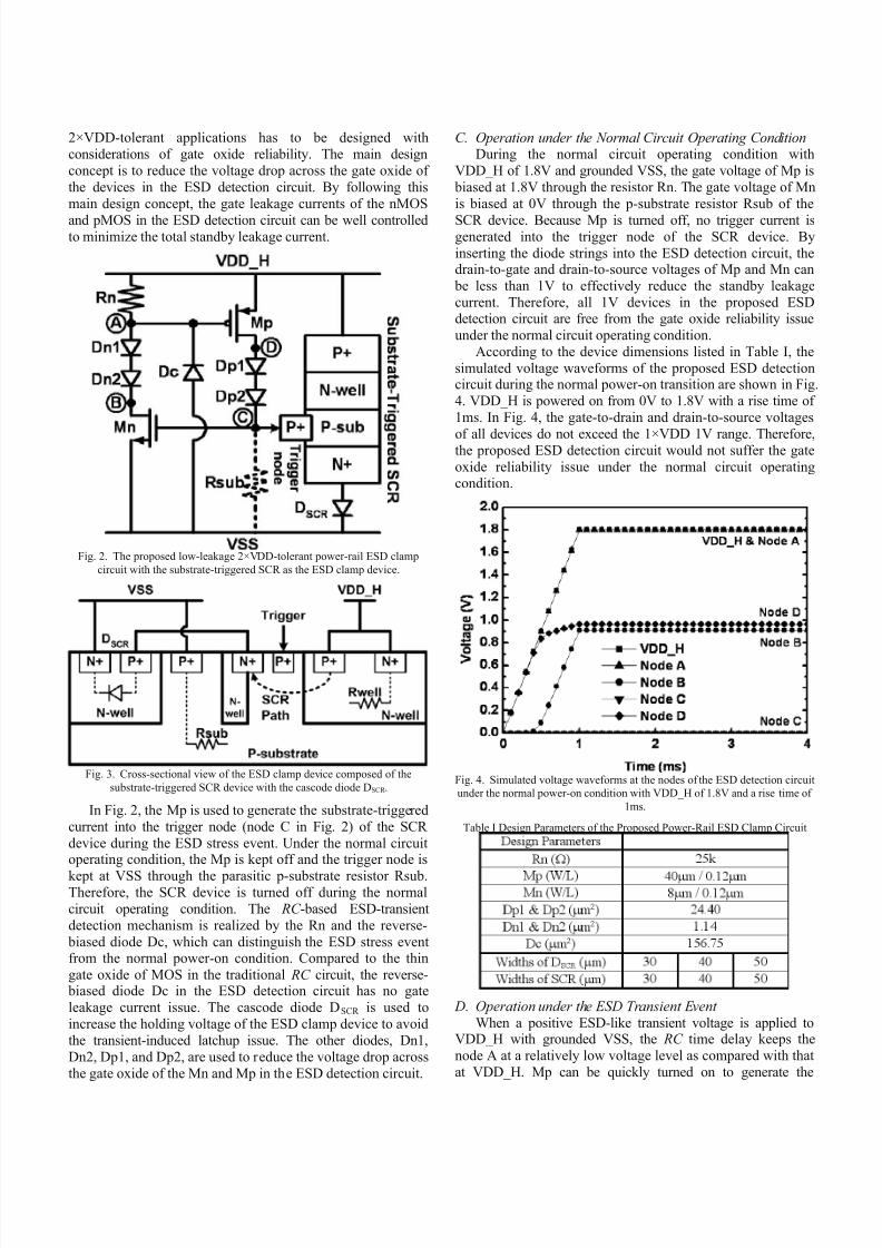
New Design on 2 ×VDD-Tolerant Power-Rail ESD Clamp Circuit with Low Standby Leakage in 65nm CMOS Process Chih-Ting Yeh 1,2 and Ming-Dou Ker 2,3 1 Informatio n and Communications Research Labo ratories, Industrial Technology Research Institute, Hsinchu, Taiwan. 2 Departme nt of Electronics Engineering & Institute of Electronics, National Chiao-Tung University, Hsinchu, Taiwan. 3 Departme nt of Electronic Engineering, I-Shou University , Kaohsiung, Taiwan. Abstract -A 2×VDD-tolerant power-rail electrostatic discharge (ESD) clamp circuit with only thin gate oxide 1V devices and silicon-controlled rectifier (SCR) as main ESD clamp device has been proposed and verified in a 65nm CMOS process. The proposed power-rail ESD clamp circuit has an ultra-low standby leakage current by reducing the voltage drop across the gate oxide of the devices in the ESD detection circuit. From the measured results, the proposed design with SCR dimension of 50µm in width can achieve 6.5kV human-body-model (HBM), 300V machine-model (MM) ESD levels, and an ultra-low standby leakage current of 34.1nA at room temperature under the normal circuit operating condition with 1.8V bias. I. I NTRODUCTION With the continuously progressed CMOS technology, the number of transistors in a chip is aggressively increasing. Therefore, the system-on-a-chip (SoC) has become popular. For SoC integration, the input/output (I/O) circuits may receive or drive high-voltage signals to communicate with other integrated circuits (ICs) in a microelectronic system. However, the nanoscale device with thinner gate oxide and shallower diffusion junction depth arises several serious problems when it is implemented in the I/O circuits with mixed-voltage interfaces [1]. These problems include the gate oxide reliability [2], [3] and the undesirable leakage current paths [4], [5]. In 45nm CMOS technologies and beyond, the high-K materials have gradually replaced the silicon dioxide to r educe the equivalent oxide thickness (EOT) and the gate leakage current [6], [7]. However, the 90nm and 65nm CMOS technologies, which currently do not use the high-K materials as gate oxide layer, still suffer enormous gate leakage current issue. In order to solve the gate oxide reliability in the ESD protection circuit for the mixed-voltage I/O interface s, the stacked-MOS configuration has been reported [8]. Other design strategies on high-voltage-tolerant power-rail ESD clamp circuit were also revealed to reduce the standby leakage current in nanometer CMOS technologies [9], [10]. In this work, a new low-leakage 2×VDD-tolerant power- rail ESD clamp circuit realized with only thin gate oxide devices for mixed-voltage I/O applications is proposed and verified in a 65nm CMOS technology. According to the experimental results, the standby leakage current of the proposed design can a chieve the order of n ano-ampere under the normal circuit operating condition. II. NEW PROPOSED 2×VDD-TOLERANT POWER -R AIL ESD CLAMP CIRCUIT WITH LOW STANDBY LEAKAGE A. Gate L eakage Cu rrent in Nanos cale CMOS When the gate oxide thickness continuously scales down in advanced CMOS technology, the gate leakage current has become an inevitable issue. Based on the BSIM4 model [11] with the device parameters provided from foundry, the gate currents of the nMOS capacitors in 65nm and 90nm CMOS technologies are compared in Fig. 1. The gate currents of the nMOS capacitors with W/L of 5 µm/5µm and 10µm/10µm are 217nA and 878nA (1.61µA and 6.48µA) at 1V in 90nm (65nm) technology, respectively. The gate current of the nMOS capacitor is directly dependent on the poly-gate area and the gate oxide thickness. Therefore, the gate leakage issue in 65nm CMOS technology is much worse than that in 90nm CMOS technology due to thinner gate oxide. Fig. 1. Simulated gate currents of the nMOS capacitors in 65nm and 90nm CMOS technologies. B. Design Concept of New Proposed 2×VDD-Toleran t Power-Ra il ESD Cl amp Circu it The proposed 2×VDD-tolerant power-rail ESD clamp circuit with the substrate-triggered SCR device [12] as the main ESD clamp device is shown in Fig. 2. The cross- sectional view of the substrate-triggered SCR device is also illustrated in Fig. 3. The SCR device without the poly-gate structure has very small leakage current. The ESD detection circuit is necessary to improve the turn-on speed of the SCR device under ESD stress condition. Therefore, the proposed ESD detection circuit with only thin gate oxide 1V devices for 978-1-4577-2081-9/12/$26.00 ©2012 IEEE


![VD V D G C G C A Low Dynamic Power and Low …27.3 78 48.4 48.2 N-SR-S/C-SR (%) Stand-by power, PST [nW] 1,147 275.6 34.0 484.0 131.9 132.0 Active power, PAT [µW] at fc = 570 MHz](https://img.pdfslide.us/doc/110x75/5f14ed87b291d0621c2683f2/vd-v-d-g-c-g-c-a-low-dynamic-power-and-low-273-78-484-482-n-sr-sc-sr-stand-by.jpg)