Embed Size (px)
Citation preview
Low Power, High Output Current, Quad Op Amp, Dual-Channel ADSL/ADSL2+ Line Driver
Data Sheet AD8392A
Rev. A Document Feedback Information furnished by Analog Devices is believed to be accurate and reliable. However, no responsibility is assumed by Analog Devices for its use, nor for any infringements of patents or other rights of third parties that may result from its use. Specifications subject to change without notice. No license is granted by implication or otherwise under any patent or patent rights of Analog Devices. Trademarks and registered trademarks are the property of their respective owners.
One Technology Way, P.O. Box 9106, Norwood, MA 02062-9106, U.S.A.Tel: 781.329.4700 ©2006–2016 Analog Devices, Inc. All rights reserved. Technical Support www.analog.com
FEATURES Four current feedback, high current amplifiers Ideal for use as ADSL/ADSL2+ dual-channel central office
(CO) line drivers Low power operation
Power supply operation from ±5 V (+10 V) up to ±12 V (+24 V) Less than 3 mA/amp quiescent supply current for full
power ADSL/ADSL2+ CO applications (20.4 dBm line power, 5.5 CF)
Three active power modes plus shutdown High output voltage and current drive
500 mA peak output drive current 42.6 V p-p differential output voltage
Low distortion −93 dBc @1 MHz second harmonic −103 dBc @ 1 MHz third harmonic
High speed: 515 V/μs differential slew rate Additional functionality of AD8392AACP
On-chip, common-mode voltage generation APPLICATIONS ADSL/ADSL2+ CO line drivers XDSL line drivers GENERAL DESCRIPTION
The AD8392A is comprised of four high output current, low power consumption, operational amplifiers. It is particularly well suited for the CO driver interface in digital subscriber line systems, such as ADSL and ADSL2+. The driver is capable of providing enough power to deliver 20.4 dBm to a line, while compensating for losses due to hybrid insertion and back termination resistors.
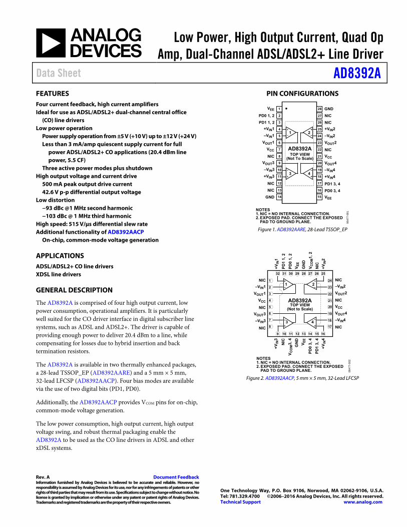
The AD8392A is available in two thermally enhanced packages, a 28-lead TSSOP_EP (AD8392AARE) and a 5 mm × 5 mm, 32-lead LFCSP (AD8392AACP). Four bias modes are available via the use of two digital bits (PD1, PD0).
Additionally, the AD8392AACP provides VCOM pins for on-chip, common-mode voltage generation.
The low power consumption, high output current, high output voltage swing, and robust thermal packaging enable the AD8392A to be used as the CO line drivers in ADSL and other xDSL systems.
PIN CONFIGURATIONS
1
2
3
4
5
6
7
8
9
10
11
12
13
14
28
27
26
25
24
23
22
21
20
19
18
17
16
15
AD8392ATOP VIEW
(Not To Scale)
PD0 1, 2
PD1 1, 2
+VIN1
NIC
VOUT1
–VIN1
VEE
NIC
NIC
+VIN2
NIC
VOUT2
–VIN2
VOUT3
–VIN3
+VIN3
GND
NIC
NIC
VCC
–VIN4
+VIN4
VEE
PD0 3, 4
PD1 3, 4
GND
VCC
VOUT4
1
3 4
2
0647
7-00
1NOTES1. NIC = NO INTERNAL CONNECTION.2. EXPOSED PAD. CONNECT THE EXPOSED
PAD TO GROUND PLANE. Figure 1. AD8392AARE, 28-Lead TSSOP_EP
1
2
3
4
5
6
7
8
24
23
22
21
20
19
18
17
AD8392ATOP VIEW
(Not to Scale)
+V
IN1
NIC
VOUT1
–VIN1
VE
E
NIC
+V
IN2
NIC
VOUT2
–VIN2
VOUT3
–VIN3
+V
IN3
GN
D
NIC
VCC
–VIN4+
VIN
4
VE
E
PD
0 3,
4
GN
DVCC
VOUT4
NIC
NIC
NIC
NIC
VC
OM
3, 4
PD
1 3,
4
VC
OM
1, 2
PD
1 1,
2
PD
0 1,
2
3 4
0647
7-00
2
32 31 30 29 28 27 2526
9 10 11 12 13 14 1615
1 2
NOTES1. NIC = NO INTERNAL CONNECTION.2. EXPOSED PAD. CONNECT THE EXPOSED
PAD TO GROUND PLANE. Figure 2. AD8392AACP, 5 mm × 5 mm, 32-Lead LFCSP
AD8392A Data Sheet
Rev. A | Page 2 of 12
TABLE OF CONTENTS Features .............................................................................................. 1
Applications ....................................................................................... 1
General Description ......................................................................... 1
Pin Configurations ........................................................................... 1
Revision History ............................................................................... 2
Specifications ..................................................................................... 3
Absolute Maximum Ratings ............................................................ 4
Thermal Resistance ...................................................................... 4
ESD Caution .................................................................................. 4
Typical Performance Characteristics ............................................. 5
Theory of Operation ........................................................................ 7
Applications ........................................................................................8
Supplies, Grounding, and Layout ................................................8
Power Management ......................................................................8
Thermal Considerations ...............................................................8
Typical ADSL/ADSL2+ Application ...........................................9
Multitone Power Ratio ............................................................... 10
Outline Dimensions ....................................................................... 11
Ordering Guide .......................................................................... 11
Notes ................................................................................................. 12
REVISION HISTORY
6/2016—Rev. 0 to Rev. A Changed CP-32-2 to CP-32-7 ...................................... Throughout Change to Applications Section, Figure 1, and Figure 2 ............. 1 Updated Outline Dimensions ....................................................... 12 Changes to Ordering Guide .......................................................... 12 10/2006—Revision 0: Initial Version
Data Sheet AD8392A
Rev. A | Page 3 of 12
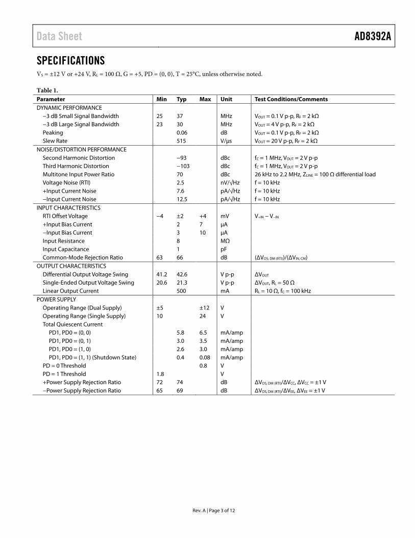
SPECIFICATIONS VS = ±12 V or +24 V, RL = 100 Ω, G = +5, PD = (0, 0), T = 25°C, unless otherwise noted.
Table 1. Parameter Min Typ Max Unit Test Conditions/Comments DYNAMIC PERFORMANCE
−3 dB Small Signal Bandwidth 25 37 MHz VOUT = 0.1 V p-p, RF = 2 kΩ −3 dB Large Signal Bandwidth 23 30 MHz VOUT = 4 V p-p, RF = 2 kΩ Peaking 0.06 dB VOUT = 0.1 V p-p, RF = 2 kΩ Slew Rate 515 V/µs VOUT = 20 V p-p, RF = 2 kΩ
NOISE/DISTORTION PERFORMANCE Second Harmonic Distortion −93 dBc fC = 1 MHz, VOUT = 2 V p-p Third Harmonic Distortion −103 dBc fC = 1 MHz, VOUT = 2 V p-p Multitone Input Power Ratio 70 dBc 26 kHz to 2.2 MHz, ZLINE = 100 Ω differential load Voltage Noise (RTI) 2.5 nV/√Hz f = 10 kHz +Input Current Noise 7.6 pA/√Hz f = 10 kHz −Input Current Noise 12.5 pA/√Hz f = 10 kHz
INPUT CHARACTERISTICS RTI Offset Voltage −4 ±2 +4 mV V+IN − V−IN +Input Bias Current 2 7 µA −Input Bias Current 3 10 µA Input Resistance 8 MΩ Input Capacitance 1 pF Common-Mode Rejection Ratio 63 66 dB (ΔVOS, DM (RTI))/(ΔVIN, CM)
OUTPUT CHARACTERISTICS Differential Output Voltage Swing 41.2 42.6 V p-p ΔVOUT Single-Ended Output Voltage Swing 20.6 21.3 V p-p ΔVOUT, RL = 50 Ω Linear Output Current 500 mA RL = 10 Ω, fC = 100 kHz
POWER SUPPLY Operating Range (Dual Supply) ±5 ±12 V Operating Range (Single Supply) 10 24 V Total Quiescent Current
PD1, PD0 = (0, 0) 5.8 6.5 mA/amp PD1, PD0 = (0, 1) 3.0 3.5 mA/amp PD1, PD0 = (1, 0) 2.6 3.0 mA/amp PD1, PD0 = (1, 1) (Shutdown State) 0.4 0.08 mA/amp
PD = 0 Threshold 0.8 V PD = 1 Threshold 1.8 V +Power Supply Rejection Ratio 72 74 dB ΔVOS, DM (RTI)/ΔVCC, ΔVCC = ±1 V −Power Supply Rejection Ratio 65 69 dB ΔVOS, DM (RTI)/ΔVEE, ΔVEE = ±1 V

AD8392A Data Sheet
Rev. A | Page 4 of 12
ABSOLUTE MAXIMUM RATINGS
Table 2. Parameter Rating Supply Voltage ±13 V (+26 V) Power Dissipation See Figure 3 Storage Temperature Range −65°C to +150°C Operating Temperature Range −40°C to +85°C Lead Temperature (Soldering 10 sec) 300°C Junction Temperature 150°C
Stresses at or above those listed under Absolute Maximum Ratings may cause permanent damage to the product. This is a stress rating only; functional operation of the product at these or any other conditions above those indicated in the operational section of this specification is not implied. Operation beyond the maximum operating conditions for extended periods may affect product reliability.
THERMAL RESISTANCE θJA is specified for the worst-case conditions, that is, θJA is specified for the device soldered in the circuit board for surface-mount packages.
Table 3. Package Type θJA Unit LFCSP-32 (CP) 27.27 °C/W TSSOP_EP (RE) 35.33 °C/W
Maximum Power Dissipation
The power dissipated in the package (PD) is the sum of the quiescent power dissipation and the power dissipated in the package due to the load drive for all outputs. The quiescent power is the voltage between the supply pins (VS) times the quiescent current (IS). Assuming that the load (RL) is midsupply, the total drive power is VS/2 × IOUT, some of which is dissipated in the package and some in the load (VOUT × IOUT).
RMS output voltages should be considered. If RL is referenced to VS− as in single-supply operation, the total power is VS × IOUT.
In single supply with RL to VS−, worst case is VOUT = VS/2.
Airflow increases heat dissipation, effectively reducing θJA. In addition, more metal directly in contact with the package leads from metal traces, through holes, ground, and power planes reduces the θJA.
Figure 3 shows the maximum safe power dissipation in the package vs. the ambient temperature for the LFCSP-32 and TSSOP_EP packages on a JEDEC standard 4-layer board. θJA values are approximations.
0
1
2
3
4
5
6
7
–40 –30 –20 –10 0 10 20 30 40 50 60 70 80 90TEMPERATURE (°C)
MA
XIM
UM
PO
WER
DIS
SIPA
TIO
N (W
)
TJ = 150°C
LFCSP-32
TSSOP-28/EP
0647
7-00
3
Figure 3. Maximum Power Dissipation vs. Temperature for a 4-Layer Board
See the Thermal Considerations section for additional thermal design guidance.
ESD CAUTION
Data Sheet AD8392A
Rev. A | Page 5 of 12
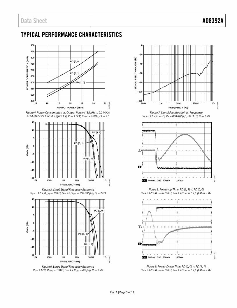
TYPICAL PERFORMANCE CHARACTERISTICS
900
45015 21
OUTPUT POWER (dBm)
POW
ER C
ON
SUM
PTIO
N (m
W)
850
800
750
700
650
600
550
500
16 17 18 19 20
PD (1, 0)
0647
7-04
6
PD (0, 0)
PD (0, 1)
Figure 4. Power Consumption vs. Output Power (138 kHz to 2.2 MHz), ADSL/ADSL2+ Circuit (Figure 15), VS = ±12 V, RLOAD = 100 Ω, CF = 5.5
15
–2010k 1G
FREQUENCY (Hz)
GA
IN (d
B)
100k 1M 10M 100M
10
5
0
–5
–10
–15
PD (0, 1)
PD (0, 0)
PD (1, 0)
0647
7-04
9
Figure 5. Small Signal Frequency Response
VS = ±12 V, RLOAD = 100 Ω, G = +5, VOUT = 100 mV p-p, RF = 2 kΩ
15
–2010k 1G
FREQUENCY (Hz)
GA
IN (d
B)
100k 1M 10M 100M
10
5
0
–5
–10
–15
PD (0, 0)
PD (0, 1)
PD (1, 0)
0647
7-04
5
Figure 6. Large Signal Frequency Response
VS = ±12 V, RLOAD = 100 Ω, G = +5, VOUT = 4 V p-p, RF = 2 kΩ
0
–120100k 1G
FREQUENCY (Hz)
SIG
NA
L FE
EDTH
RO
UG
H (d
B)
1M 10M 100M
–20
–40
–60
–80
–100
0647
7-04
8
Figure 7. Signal Feedthrough vs. Frequency
VS = ±12 V, G = +5, VIN = 800 mV p-p, PD (1, 1), RF = 2 kΩ
CH1 500mV CH2 500mV 100ns
1
2
0647
7-04
2
Figure 8. Power-Up Time: PD (1, 1) to PD (0, 0) VS = ±12 V, RLOAD = 100 Ω, G = +5, VOUT = 1 V p-p, RF = 2 kΩ
CH1 500mV CH2 500mV 400ns
1
2
0647
7-04
1
Figure 9. Power-Down Time: PD (0, 0) to PD (1, 1) VS = ±12 V, RLOAD = 100 Ω, G = +5, VOUT = 1 V p-p, RF = 2 kΩ

AD8392A Data Sheet
Rev. A | Page 6 of 12
CH1 200mV CH2 2V 400ns
2
0647
7-04
0
INPUTCHANNEL 1 OUTPUT
CHANNEL 2
Figure 10. Output Overdrive Recovery, ADSL/ADSL2+ Circuit (Figure 15), DMT Waveform, VS = ±12 V
0
–100100k 100M
FREQUENCY (Hz)
CR
OS
ST
AL
K (
dB
)
1M 10M
–10
–20
–30
–40
–50
–60
–70
–80
–90
DIFF CHANNEL 3, 4
DIFF CHANNEL 1, 2
0647
7-02
5
Figure 11. Crosstalk vs. Frequency, Dual Differential Driver Circuit (Figure 14), VS = ±12 V, VIN = 800 mV p-p
45
100 100
0647
7-05
4
LOAD RESISTANCE (Ω)
DIF
FE
RE
NT
IAL
OU
TP
UT
(V
p-p
)
40
35
30
25
20
15
10 20 30 40 50 60 70 80 90
Figure 12. Differential Output Swing vs. RLOAD Dual Differential Driver Circuit (Figure 14)
100
0.0110k 1G
FREQUENCY (Hz)
OU
TP
UT
IM
PE
DA
NC
E (Ω
)
100k 1M 10M 100M
0.1
1
10
PD (0, 0)
PD (1, 0) PD (0, 1)
0647
7-04
7
Figure 13. Output Impedance vs. Frequency VS = ±12 V, G = +5, RF = 2 kΩ
2kΩ
2kΩ
499Ω
49.9Ω
49.9Ω
100Ω
0647
7-05
3
Figure 14. Dual Differential Driver Circuit
2kΩ
2kΩ
4.99Ω
4.99Ω
1.78kΩ
1.78kΩ
634Ω
634Ω
1µF
87Ω
87Ω77Ω
77Ω
0.01µF
0.01µF
100ΩVCM
0647
7-02
1
Figure 15. ADSL/ADSL2+ Circuit
Data Sheet AD8392A
Rev. A | Page 7 of 12
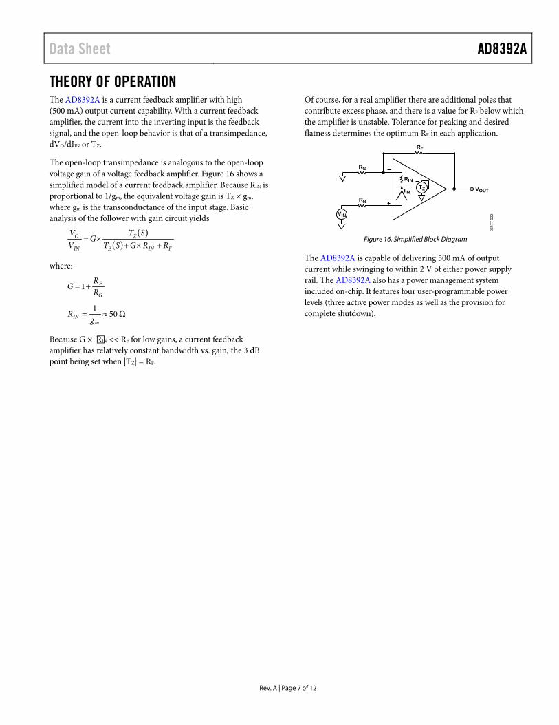
THEORY OF OPERATION The AD8392A is a current feedback amplifier with high (500 mA) output current capability. With a current feedback amplifier, the current into the inverting input is the feedback signal, and the open-loop behavior is that of a transimpedance, dVO/dIIN or TZ.
The open-loop transimpedance is analogous to the open-loop voltage gain of a voltage feedback amplifier. Figure 16 shows a simplified model of a current feedback amplifier. Because RIN is proportional to 1/gm, the equivalent voltage gain is TZ × gm, where gm is the transconductance of the input stage. Basic analysis of the follower with gain circuit yields
( )( ) FINZ
Z
IN
O
RRGSTST
GVV
+×+×=
where:
G
F
RR
G +=1
Ω501
≈=m
IN gR
Because G × RIN << RF for low gains, a current feedback amplifier has relatively constant bandwidth vs. gain, the 3 dB point being set when |TZ| = RF.
Of course, for a real amplifier there are additional poles that contribute excess phase, and there is a value for RF below which the amplifier is unstable. Tolerance for peaking and desired flatness determines the optimum RF in each application.
0647
7-02
2
RF
VOUT
RG
RN
VIN
RIN
IINTZ
Figure 16. Simplified Block Diagram
The AD8392A is capable of delivering 500 mA of output current while swinging to within 2 V of either power supply rail. The AD8392A also has a power management system included on-chip. It features four user-programmable power levels (three active power modes as well as the provision for complete shutdown).

AD8392A Data Sheet
Rev. A | Page 8 of 12
APPLICATIONS SUPPLIES, GROUNDING, AND LAYOUT The AD8392A can be powered from either single or dual supplies, with the total supply voltage ranging from 10 V to 24 V. For optimum performance, a well regulated low ripple supply should be used.
As with all high speed amplifiers, close attention should be paid to supply decoupling, grounding, and overall board layout. Low frequency supply decoupling should be provided with 10 µF tantalum capacitors from each supply to ground. In addition, all supply pins should be decoupled with 0.1 µF quality ceramic chip capacitors placed as close as possible to the driver. An internal low impedance ground plane should be used to provide a common ground point for all driver and decoupling capacitor ground requirements. Whenever possible, separate ground planes should be used for analog and digital circuitry.
High speed layout techniques should be followed to minimize parasitic capacitance around the inverting inputs. Some practical examples of these techniques are keeping feedback traces as short as possible and clearing away ground plane in the area of the inverting inputs. Input and output traces should be kept short and as far apart from each other as practical to avoid crosstalk. When used as a differential driver, all differential signal traces should be kept as symmetrical as possible.
POWER MANAGEMENT The AD8392A can be configured in any of three active bias states as well as a shutdown state via the use of two sets of digitally programmable logic pins. Pin PD0 (1, 2) and Pin PD1 (1, 2) control Amplifier 1 and Amplifier 2, while PD0 (3, 4) and Pin PD1 (3, 4) control Amplifier 3 and Amplifier 4. These pins can be controlled directly with either 3.3 V or 5 V CMOS logic by using the GND pins as a reference. If left unconnected, the PD pins float low, placing the amplifier in the full bias mode. Refer to the Specifications for the per amplifier quiescent current for each of the available bias states.
As is shown in Figure 13, the AD8392A exhibits low output impedance for the three active states. The shutdown state (PD1, PD0 = 1, 1) provides a high impedance output.
THERMAL CONSIDERATIONS When using a quad, high output current amplifier, such as the AD8392A, special consideration should be given to system level thermal design. In applications such as the ADSL/ADSL2+, the AD8392A could be required to dissipate as much as 1.4 W or more on-chip. Under these conditions, particular attention should be paid to the thermal design to maintain safe operating temperatures on the die. To aid in the thermal design, the thermal information in the Thermal Resistance section can be combined with what follows here.
The information in Table 3 and Figure 3 is based on a standard JEDEC 4-layer board and a maximum die temperature of 150°C. To provide additional guidance and design suggestions, a thermal study was performed under a set of conditions more closely aligned with an actual ADSL/ADSL2+ application.
In a typical ADSL/ADSL2+ line card, component density usually dictates that most of the copper plane used for thermal dissipation be internal. Additionally, each ADSL/ADSL2+ port may be allotted only 1 square inch, or even less, of board space. For these reasons, a special thermal test board was constructed for this study. The 4-layer board measured approximately 4 inches × 4 inches and contained two internal 1 oz copper ground planes, each measuring 2 inches × 3 inches. The top layer contained signal traces and an exposed copper strip ¼ inch × 3 inches to accommodate heat sinking, with no other copper on the top or bottom of the board.
Three 28-lead TSSOPs were placed on the board representing six ADSL channels, or one channel per square inch of copper, with each channel dissipating 700 mW on-chip (1.4 W per package). The die temperature is then measured in still air and in a wind tunnel with calibrated airflow of 100 LFM, 200 LFM, and 400 LFM. Figure 17 shows the power dissipation vs. the ambient temperature for each airflow condition. The figure assumes a maximum die temperature of 135°C. No heat sink was used.
1.0
1.5
2.0
2.5
3.0
3.5
4.0
4.5
5 15 25 35 45 55 65 75 85AMBIENT TEMPERATURE (°C)
POW
ER D
ISSI
PATI
ON
(W)
TJ = 135°C
0647
7-05
1
STILL AIR100LFM
200LFM
400LFM
Figure 17. Power Dissipation vs. Ambient
Temperature and Air Flow 28-Lead TSSOP/EP
This data is only provided as guidance to assist in the thermal design process. Due diligence should be performed with regards to power dissipation because there are many factors that can affect thermal performance.
Data Sheet AD8392A
Rev. A | Page 9 of 12
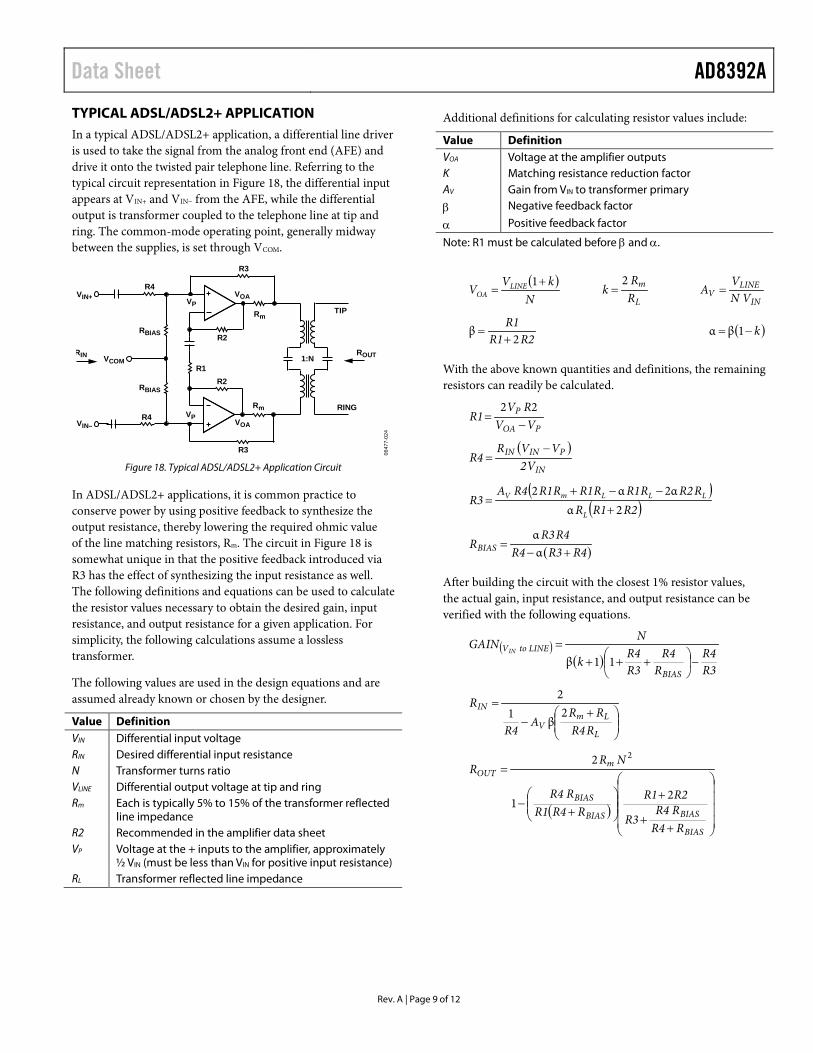
TYPICAL ADSL/ADSL2+ APPLICATION In a typical ADSL/ADSL2+ application, a differential line driver is used to take the signal from the analog front end (AFE) and drive it onto the twisted pair telephone line. Referring to the typical circuit representation in Figure 18, the differential input appears at VIN+ and VIN− from the AFE, while the differential output is transformer coupled to the telephone line at tip and ring. The common-mode operating point, generally midway between the supplies, is set through VCOM.
R4
R4
R3
R3
Rm
R2R1
R2
VCOM 1:N
TIP
RING
ROUTRIN
Rm
VOA
VOAVP
VP
RBIAS
RBIAS
VIN–
VIN+
0647
7-02
4
Figure 18. Typical ADSL/ADSL2+ Application Circuit
In ADSL/ADSL2+ applications, it is common practice to conserve power by using positive feedback to synthesize the output resistance, thereby lowering the required ohmic value of the line matching resistors, Rm. The circuit in Figure 18 is somewhat unique in that the positive feedback introduced via R3 has the effect of synthesizing the input resistance as well. The following definitions and equations can be used to calculate the resistor values necessary to obtain the desired gain, input resistance, and output resistance for a given application. For simplicity, the following calculations assume a lossless transformer.
The following values are used in the design equations and are assumed already known or chosen by the designer.
Value Definition VIN Differential input voltage RIN Desired differential input resistance N Transformer turns ratio VLINE Differential output voltage at tip and ring Rm Each is typically 5% to 15% of the transformer reflected
line impedance R2 Recommended in the amplifier data sheet VP Voltage at the + inputs to the amplifier, approximately
½ VIN (must be less than VIN for positive input resistance) RL Transformer reflected line impedance
Additional definitions for calculating resistor values include:
Value Definition VOA Voltage at the amplifier outputs K Matching resistance reduction factor AV Gain from VIN to transformer primary
β Negative feedback factor
α Positive feedback factor
Note: R1 must be calculated before β and α.
( )N
kVV LINE
OA+
=1
L
m
RR
k2
= IN
LINEV VN
VA =
R2R1R1
2β
+= ( )k−= 1βα
With the above known quantities and definitions, the remaining resistors can readily be calculated.
POA
P
VVRV
R1−
=22
( )IN
PININ
V2VVR
R4−
=
( )( )R2R1R
RR2RR1RR1RR1R4AR3
L
LLLmV
2α2αα2
+−−+
=
( )R4R3R4R4R3
RBIAS +−=
αα
After building the circuit with the closest 1% resistor values, the actual gain, input resistance, and output resistance can be verified with the following equations.
( )( )
R3R4
RR4
R3R4
k
NGAIN
BIAS
LINEtoVIN
−
+++
=11β
+−
=
L
LmV
IN
RR4RR
AR4
R2
β1
2
( )
++
+
+
−
=
BIAS
BIASBIAS
BIAS
mOUT
RR4RR4
R3
R2R1RR4R1
RR4
NRR
21
2 2
AD8392A Data Sheet
Rev. A | Page 10 of 12
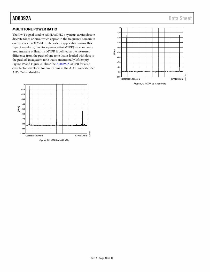
MULTITONE POWER RATIO The DMT signal used in ADSL/ADSL2+ systems carries data in discrete tones or bins, which appear in the frequency domain in evenly spaced 4.3125 kHz intervals. In applications using this type of waveform, multitone power ratio (MTPR) is a commonly used measure of linearity. MTPR is defined as the measured difference from the peak of one tone that is loaded with data to the peak of an adjacent tone that is intentionally left empty. Figure 19 and Figure 20 show the AD8392A MTPR for a 5.5 crest factor waveform for empty bins in the ADSL and extended ADSL2+ bandwidths.
0
–100CENTER 646.9kHz SPAN 10kHz
(dB
m)
–10
–20
–30
–40
–50
–60
–70
–80
–90
0647
7-04
3
Figure 19. MTPR at 647 kHz
0
–100CENTER 1.9664kHz SPAN 10kHz
(dB
m)
–10
–20
–30
–40
–50
–60
–70
–80
–90
0647
7-04
4
Figure 20. MTPR at 1.966 MHz
Data Sheet AD8392A
Rev. A | Page 11 of 12
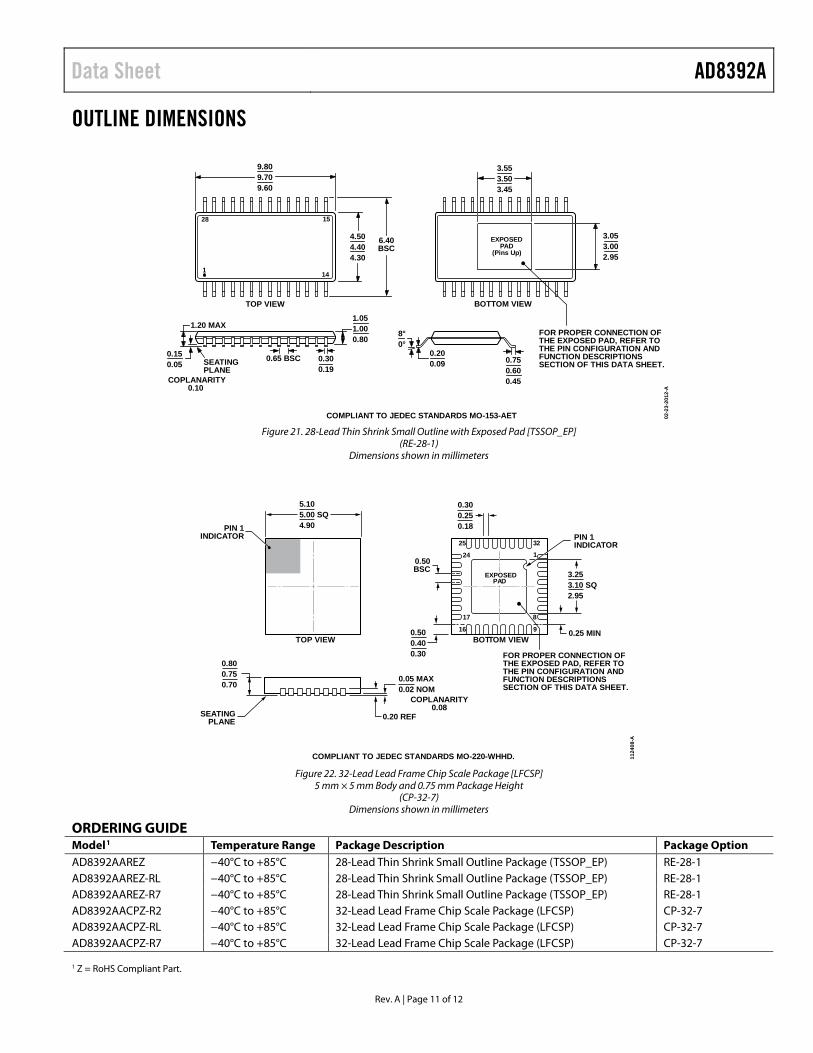
OUTLINE DIMENSIONS
COMPLIANT TO JEDEC STANDARDS MO-153-AET
28 15
141
EXPOSEDPAD
(Pins Up)
9.809.709.60
4.504.404.30
6.40BSC
TOP VIEW BOTTOM VIEW
0.65 BSC0.150.05
COPLANARITY0.10
1.20 MAX1.051.000.80
0.300.19
SEATINGPLANE
0.200.09
3.053.002.95
8°0°
0.750.600.45
3.553.503.45
02-2
3-20
12-A
FOR PROPER CONNECTION OFTHE EXPOSED PAD, REFER TOTHE PIN CONFIGURATION ANDFUNCTION DESCRIPTIONSSECTION OF THIS DATA SHEET.
Figure 21. 28-Lead Thin Shrink Small Outline with Exposed Pad [TSSOP_EP]
(RE-28-1) Dimensions shown in millimeters
COMPLIANT TO JEDEC STANDARDS MO-220-WHHD. 1124
08-A
10.50BSC
BOTTOM VIEWTOP VIEW
PIN 1INDICATOR
32
916
17
24
25
8
EXPOSEDPAD
PIN 1INDICATOR
3.253.10 SQ2.95
SEATINGPLANE
0.05 MAX0.02 NOM
0.20 REF
COPLANARITY0.08
0.300.250.18
5.105.00 SQ4.90
0.800.750.70
FOR PROPER CONNECTION OFTHE EXPOSED PAD, REFER TOTHE PIN CONFIGURATION ANDFUNCTION DESCRIPTIONSSECTION OF THIS DATA SHEET.
0.500.400.30
0.25 MIN
Figure 22. 32-Lead Lead Frame Chip Scale Package [LFCSP]
5 mm × 5 mm Body and 0.75 mm Package Height (CP-32-7)
Dimensions shown in millimeters
ORDERING GUIDE Model1 Temperature Range Package Description Package Option AD8392AAREZ −40°C to +85°C 28-Lead Thin Shrink Small Outline Package (TSSOP_EP) RE-28-1 AD8392AAREZ-RL −40°C to +85°C 28-Lead Thin Shrink Small Outline Package (TSSOP_EP) RE-28-1 AD8392AAREZ-R7 −40°C to +85°C 28-Lead Thin Shrink Small Outline Package (TSSOP_EP) RE-28-1 AD8392AACPZ-R2 −40°C to +85°C 32-Lead Lead Frame Chip Scale Package (LFCSP) CP-32-7 AD8392AACPZ-RL −40°C to +85°C 32-Lead Lead Frame Chip Scale Package (LFCSP) CP-32-7 AD8392AACPZ-R7 −40°C to +85°C 32-Lead Lead Frame Chip Scale Package (LFCSP) CP-32-7 1 Z = RoHS Compliant Part.

AD8392A Data Sheet
Rev. A | Page 12 of 12
NOTES
©2006–2016 Analog Devices, Inc. All rights reserved. Trademarks and registered trademarks are the property of their respective owners. D06477-0-6/16(A)