Embed Size (px)
Citation preview
@IJRTER-2017, All Rights Reserved 537
Low Power Gating Scan Cell For Shift Power
Reduction Considering Both This Scan Chain And
Combinational Part
Y MOHITHA
Student, ECE Department
Nalla Narasimha Reddy Educational Society’s
Group of Institutions
B SWATHI
Student, ECE Department
Nalla Narasimha Reddy Educational Society’s
Group of Institutions
Abstract: Excessive power consumption during
test application time has severely negative effects
on chip reliability since it has an inevitable role
in hot spots that appear, degradation of
performance, circuit premature destruction, and
functional failures. In scan-based designs,
rippling transitions caused by test patterns
shifting along the scan chain not only elevate
power consumption in the scan chain but also
introduce spurious switching activities in the
combinational logic. In this work, a new low
power gating scan cell for scan based designs
has been proposed in order to reduce power
consumption in the scan chain as well as the
combinational part during shifting. We have
modified the conventional scan cell and
augmented it with state preserving and gating
logic that enables an average power reduction in
combinational logic during shift mode. The new
scan cell mitigates the number of transitions
during shift and capture cycles. Thus, it reduces
the average power consumption inside the scan
cell and as a result the scan chain during scan
shifting with a low impact on peak power
during the capture cycle. Furthermore, due to
introducing a new shorter shift path,
improvements are observed in terms of
propagation delay and power consumption in the
scan chain during shifting. This leads to higher
feasible shift frequency whereby the shift
frequency is limited by the maximum power
budget and hence results in reducing the test
application time. The post-layout spice
simulation results show a 7.21% reduction in
total power consumption, an average 12.25%
reduction of shift power consumption, and a
50.7% improvement in the clock (CLK)-to-shift
propagation delay over the conventional scan
cell in Synopsys 32/28 nm standard CMOS
technology.
Keywords: switching activity; scan cell; gating logic; shift power; peak power; design for testability
Introduction
The most major concerns regarding challenges
to test current high integration density circuits are
the test cost and test power. On one hand, product
quality requires the execution of high quality
manufacturing tests and diagnostics. Such a high
quality test procedure can elevate the test
application time that results in high test cost. The
standard scan is one of the most widely employed
design-for-testability (DFT) approaches that offers a
high quality test procedure by providing
controllability and observability on every single
storage element in the circuit-under-test (CUT).
Unfortunately, scan-based architectures are very
expensive in terms of power, as each scan test pattern
contributes to a shift operation with high power
consumption. Power consumption during testing is
significantly higher than that during the normal
operation. Since there is less correlation between
scan test vectors generated by an Automatic Test
Pattern Generation (ATPG) tool compared to the
data during normal mode, high switching activities
incurred in capture mode have increased the test
power drastically over the chip power threshold.
On the other hand, high test power consumption
not only increases the test cost, but also may cause
reliability hazards or even instant damages.
Reducing the switching activities at any instant of
time mitigates the average power and hence the
peak power of the chip. Moreover, the peak power
and average power reduction during testing
contributes to enhanced reliability of the test and
improvement of the yield.
RECENT ADVANCES IN ELECTRONICS AND COMMUNICATION ENGINEERING-2017(RAECE-2017)
@IJRTER-2017, All Rights Reserved 538
In this paper, the following features is presented
as:
• Gating redundant transitions from the scan cell to combinational logic during shift mode.
• Reducing switching activity inside the scan cell during shift mode.
In order to achieve the above mentioned features
within an integrated structure, we have modified
the slave latch in the conventional master/slave
scan cell with state preserving and gating abilities.
The proposed gating scan architecture introduces
a new short shift path that improves both shift
and capture propagation delays as well as power
consumption in the scan chain during shift mode.
This makes shifting at higher frequency possible
in those cases where the maximum shift frequency
has been bounded by the maximum allowable
power consumption. Therefore, the proposed
gating scheme improves the test application time
over existing gating solutions. Since state
preserving and gating logics have been embedded
as part of the slave latch in the proposed gating
scan cell, the area overhead is as low as two
transistors that are sharable by several scan cells.
The proposed structure contributes to the average
power reduction in the scan architecture
(combinational logic and scan chain) during shift
mode while not causing high peak power during
capture mode. In gating methods, the main source
of excessive peak power during capture mode is
the switching activities in the gating elements
when the mode changes from shift to capture
mode or vice versa. Excessive peak power can be
avoided by reducing the level of switching activity
during testing. Therefore, the proposed structure
is able to control the peak power violations by
reducing the switching activities in other parts of
the scan cells.
Power Estimation in Digital VLSI Circuits:
Regardless of short-circuit power which is
consumed due to the short-circuit current flows
between the supply voltage and ground during
the slice time when all of the gate inputs are
active, dynamic power is consumed during the
charging and discharging of the output and
internal nodes capacitance, which can be given
by Equation (1):
where, Pdyno and Pdynj correspond to the dynamic
power consumption at the output load capacitance and the internal nodes capacitance, respectively. The switching activity at gate i output and that at the jth internal node of the ith gate are represented by αi and αij, respectively. Vij corresponds to the
voltage swing which is generally equal to VDD-Vth. Finally, CLi and Cij are used for gate i load
capacitance and the jth internal capacitance at gate
i. The average power consumption is the total energy consumption divided by the test time. This parameter is even more important than the energy as hot spots and reliability problems may be caused by constantly high power consumption. The average power consumed during the test session is presented by Equation (2), where T is the clock period and L is the total number of clocks during the test phase.
Paverage = Etotal/(L·T) (2)
The peak power consumption corresponds to the
highest amount of power consumption during
one clock cycle. If the peak power exceeds the
circuit power threshold for several clock cycles,
the correct function of the entire circuit is no
longer guaranteed. Peak power can be expressed
as follows :
Ppeak = Max Pinst(Vk)
= Maxk (Evk/tsmall) (3)
where, Pinst(Vk) (instantaneous power)
determines the amount of power consumed during a small instant of time tsmall after the
application of the test vector Vk. Evk corresponds
to the energy consumed in the circuit after application of successive input vectors (Vk−1,Vk).
1. Overview of Hardware-Based Test Power Reduction Approaches
A significant number of techniques that attempt
to reduce power in the combinational part or
scan chain during the test application time fall
into the category of hardware-based approaches.
The hardware-based approaches require
additional hardware to be added into the design,
and are easy to be integrated with different
embedded compression techniques. Clock gating
is one of the well-known power reduction
techniques in the wide range of hardware-based
methods.
RECENT ADVANCES IN ELECTRONICS AND COMMUNICATION ENGINEERING-2017(RAECE-2017)
@IJRTER-2017, All Rights Reserved 539
This method offers an algorithm for constructing
an activity-sensitive clock tree that combines nodes
with the same activity pattern to disconnect the
clock signal efficiently. The clock skew problem in
the normal mode of operation is the main
disadvantage of the clock gating technique. In
addition, a high complexity clock controller circuit
turns out to be another drawback for this category
of hardware-based approaches. Another approach
known as scan partitioning splits the scan chain
into multiple partitions and activates only one
partition at any time interval . The partitioning
scheme limits the scan chain transitions from
propagating to combinational logic during shifting
by activating only one scan path at any time
interval. the previous partitioning approach on the
first level supply (FLS) gating approach that
extends the partitioning to capture cycle as well. To
mutually exclusively activate each segment, several
clock cycles, both in shift and capture mode, are
required which results in a higher test application
time. Both of these techniques introduce a high area
penalty due to using high complexity controlling
circuits. A segment regrouping algorithm has been
proposed by Yamato et al which identifies an
optimal combination of scan segments to be clocked
simultaneously and results in further instantaneous
shift power reduction in the scan chain. These
techniquesaim to reduce the amount of switching in
the scan chain and cannot completely prevent
redundant power loss in the combinational logic.
The drawbacks of the scan chain partitioning
approaches are: 1. They result in test time
complexity increase; 2. They may cause data
dependency problems; 3. They are depending on
complicated control circuits for the activation of the
proper partition at the right time; thus, they are
expensive in terms of area; 4. Although significant
achievement in test power reduction has been
gained due to scan chain reordering and
partitioning techniques, none of the solutions within
this category have completely eliminated spurious
switching activities in the combinational logic
during shift mode.
One of the most straight-forward methods for
shift power reduction is to reduce switching activity
in the combinational logic by isolating the stimulus
path of scan cells from combinational logic during
the shift cycle, since the major source of dynamic
power in CUT is the propagation of ripple transitions
from the scan cells to the combinational logic
during scan shifting. These methods are less
intrusive to the original designs compared with the
aforementioned approaches, and they are
independent of the test set. However, they may
degrade the performance due to the inserted logic
between the scan cells’ stimuli paths and the
combinational part. Moreover, depending on the
added logic, the high area penalty is avoidable. the
authors reported gating the stimulus paths of flip-
flops by tying the path to a constant logic ‘1’ or ‘0’
through utilizing gating logic (NOR, transmission
gate (TG), together with a pull-up or a pull-down
transistor )at the scan cells’ output, and thus
eliminated spurious switching in logic gates.
However, depending on the logic on the scan cell
output, they still may not be able to block all
switching from propagating to the combinational
logic in the beginning of the shift cycle if the logic
on the scan cell output differs from the gating logic.
Thus, the unblocked transient can still propagate to
the deeper level of the combinational logic, causing
many transitions at circuit internal lines before
reaching the steady state.
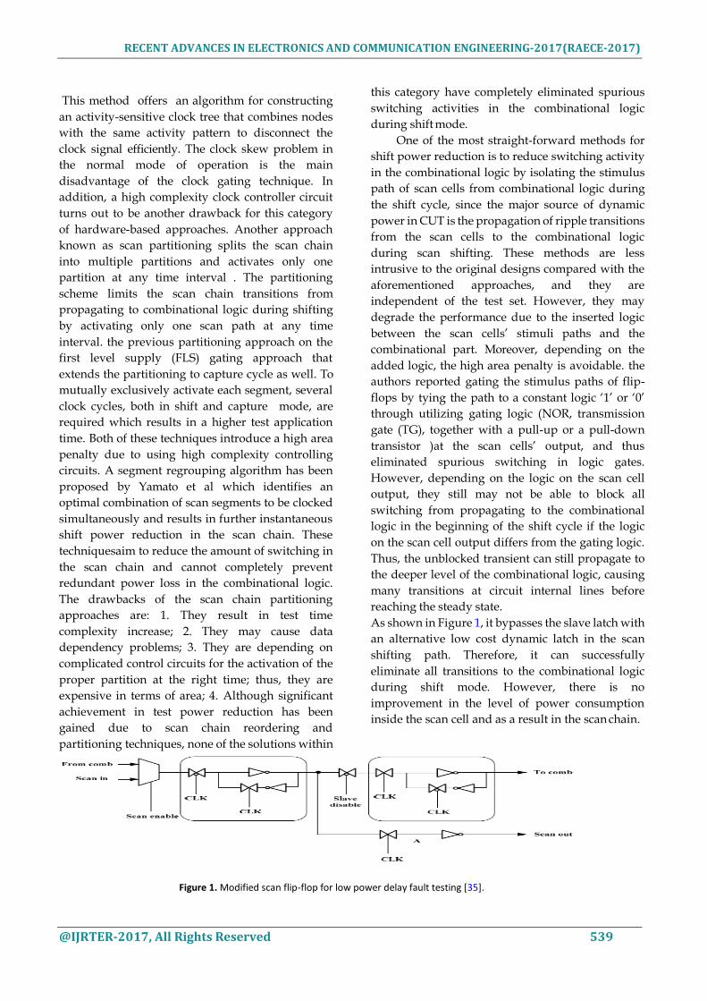
As shown in Figure 1, it bypasses the slave latch with
an alternative low cost dynamic latch in the scan
shifting path. Therefore, it can successfully
eliminate all transitions to the combinational logic
during shift mode. However, there is no
improvement in the level of power consumption
inside the scan cell and as a result in the scan chain.
Figure 1. Modified scan flip-flop for low power delay fault testing [35].

RECENT ADVANCES IN ELECTRONICS AND COMMUNICATION ENGINEERING-2017(RAECE-2017)
@IJRTER-2017, All Rights Reserved 540
Partial gating methods have been proposed to reduce
the full gating penalties in area overhead and
performance degradation. By having the proper
selection of scan cells on non-critical paths to be
gated and their gating values, they try to maximize
the shift power reduction with acceptable
performance degradation. The most recently reported
partial gating methods such as those in gate a sub-set
of scan cells not only during shift mode but also
during capture mode in order to reduce peak power
in addition to shift power reduction. However, in
large industrial designs, scan cells have large fan out
cones. Thus, un-gated scan cells in the partial gating
method can still cause a great amount of switching
activities in the combinational logic. Moreover, in both
existing full gating and partial gating techniques,
significant power is consumed in the gating elements
themselves, which causes the peak power to increase
from 5% to 60% in all the benchmark circuits when the
gating overhead was considered . This is due to the
large switching activity occurring in the gating logic
when the scan mode changes to capture mode or vice
versa . The missing part of both existing full gating
and partial gating methods is that they have limited
their approaches only to power reduction in
combinational circuits during shift cycles without
highlighting that shift power consumption is also
related to the total amount of power consumed in the
scan chain besides combinational logic.
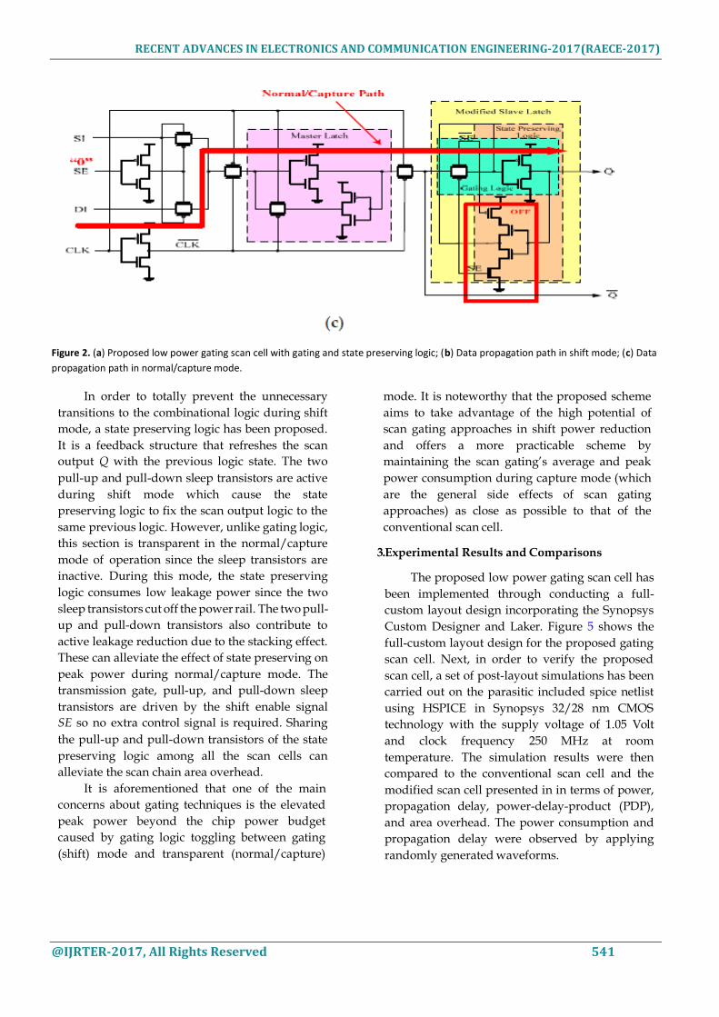
2. Proposed Low Power Gating Scan Cell
During the shift cycle, the rippling transitions
cause great switching activities in the scan chain. The
propagation of this switching activity into the
combinational part contributes to large redundant
transitions in the circuit lines. In order to suppress the
scan chain transitions from propagating during shift
cycles, we have proposed a low power gating scan
cell which contains a modified slave latch augmented
by a gating logic. For constructing the gating logic,
we have utilized a transmission gate and an inverter
to gate the scan output to the combinational logic as
illustrated in Figure 2a. It uses the transmission gate to
cut off the connection between the inverted scan cell
output Q and the output Q of the scan cells during
shift mode. As a result, the switching activities on the
Q during shift mode does not affect the scan cell
output Q which is used for driving the combinational
logic. High resistance offered by an inactive
transmission gate reduces the leakage current in the
transmission gate during shift mode and the
response capture cycle since the transmission gate is
idling in these intervals. In addition, the
transmission gate is a strong driver that feeds the
gating logic inverter and pseudo primary inputs
during normal/capture mode. Figure 2a–c depicts the
proposed low power gating scan cell and the data
propagation paths during shift and normal/capture
modes of operation, respectively.
RECENT ADVANCES IN ELECTRONICS AND COMMUNICATION ENGINEERING-2017(RAECE-2017)
@IJRTER-2017, All Rights Reserved 541
Figure 2. (a) Proposed low power gating scan cell with gating and state preserving logic; (b) Data propagation path in shift mode; (c) Data
propagation path in normal/capture mode.
In order to totally prevent the unnecessary
transitions to the combinational logic during shift
mode, a state preserving logic has been proposed.
It is a feedback structure that refreshes the scan
output Q with the previous logic state. The two
pull-up and pull-down sleep transistors are active
during shift mode which cause the state
preserving logic to fix the scan output logic to the
same previous logic. However, unlike gating logic,
this section is transparent in the normal/capture
mode of operation since the sleep transistors are
inactive. During this mode, the state preserving
logic consumes low leakage power since the two
sleep transistors cut off the power rail. The two pull-
up and pull-down transistors also contribute to
active leakage reduction due to the stacking effect.
These can alleviate the effect of state preserving on
peak power during normal/capture mode. The
transmission gate, pull-up, and pull-down sleep
transistors are driven by the shift enable signal
SE so no extra control signal is required. Sharing
the pull-up and pull-down transistors of the state
preserving logic among all the scan cells can
alleviate the scan chain area overhead.
It is aforementioned that one of the main
concerns about gating techniques is the elevated
peak power beyond the chip power budget
caused by gating logic toggling between gating
(shift) mode and transparent (normal/capture)
mode. It is noteworthy that the proposed scheme
aims to take advantage of the high potential of
scan gating approaches in shift power reduction
and offers a more practicable scheme by
maintaining the scan gating’s average and peak
power consumption during capture mode (which
are the general side effects of scan gating
approaches) as close as possible to that of the
conventional scan cell.
3.Experimental Results and Comparisons
The proposed low power gating scan cell has
been implemented through conducting a full-
custom layout design incorporating the Synopsys
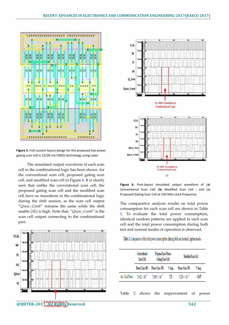
Custom Designer and Laker. Figure 5 shows the
full-custom layout design for the proposed gating
scan cell. Next, in order to verify the proposed
scan cell, a set of post-layout simulations has been
carried out on the parasitic included spice netlist
using HSPICE in Synopsys 32/28 nm CMOS
technology with the supply voltage of 1.05 Volt
and clock frequency 250 MHz at room
temperature. The simulation results were then
compared to the conventional scan cell and the
modified scan cell presented in in terms of power,
propagation delay, power-delay-product (PDP),
and area overhead. The power consumption and
propagation delay were observed by applying
randomly generated waveforms.
RECENT ADVANCES IN ELECTRONICS AND COMMUNICATION ENGINEERING-2017(RAECE-2017)
@IJRTER-2017, All Rights Reserved 542
Figure 5. Full-custom layout design for the proposed low power
gating scan cell in 32/28 nm CMOS technology using Laker.
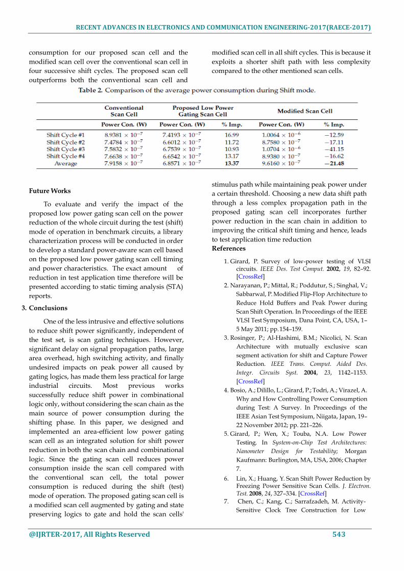
The simulated output waveform of each scan
cell to the combinational logic has been shown for
the conventional scan cell, proposed gating scan
cell, and modified scan cell in Figure 6. It is clearly
seen that unlike the conventional scan cell, the
proposed gating scan cell and the modified scan
cell have no transitions in the combinational logic
during the shift session, as the scan cell output
“Qnew_Comb” remains the same while the shift
enable (SE) is high. Note that, “Qnew_Comb” is the
scan cell output connecting to the combinational
part.
Figure 6. Post-layout simulated output waveform of (a)
Conventional Scan Cell; (b) Modified Scan Cell ; and (c)
Proposed Gating Scan Cell at 250 MHz clock frequency
The comparative analysis results on total power
consumption for each scan cell are shown in Table
1. To evaluate the total power consumption,
identical random patterns are applied to each scan
cell and the total power consumption during both
test and normal modes of operation is observed.
Table 2 shows the improvement of power
RECENT ADVANCES IN ELECTRONICS AND COMMUNICATION ENGINEERING-2017(RAECE-2017)
@IJRTER-2017, All Rights Reserved 543
consumption for our proposed scan cell and the
modified scan cell over the conventional scan cell in
four successive shift cycles. The proposed scan cell
outperforms both the conventional scan cell and
modified scan cell in all shift cycles. This is because it
exploits a shorter shift path with less complexity
compared to the other mentioned scan cells.
Future Works
To evaluate and verify the impact of the
proposed low power gating scan cell on the power
reduction of the whole circuit during the test (shift)
mode of operation in benchmark circuits, a library
characterization process will be conducted in order
to develop a standard power-aware scan cell based
on the proposed low power gating scan cell timing
and power characteristics. The exact amount of
reduction in test application time therefore will be
presented according to static timing analysis (STA)
reports.
3. Conclusions
One of the less intrusive and effective solutions
to reduce shift power significantly, independent of
the test set, is scan gating techniques. However,
significant delay on signal propagation paths, large
area overhead, high switching activity, and finally
undesired impacts on peak power all caused by
gating logics, has made them less practical for large
industrial circuits. Most previous works
successfully reduce shift power in combinational
logic only, without considering the scan chain as the
main source of power consumption during the
shifting phase. In this paper, we designed and
implemented an area-efficient low power gating
scan cell as an integrated solution for shift power
reduction in both the scan chain and combinational
logic. Since the gating scan cell reduces power
consumption inside the scan cell compared with
the conventional scan cell, the total power
consumption is reduced during the shift (test)
mode of operation. The proposed gating scan cell is
a modified scan cell augmented by gating and state
preserving logics to gate and hold the scan cells'
stimulus path while maintaining peak power under
a certain threshold. Choosing a new data shift path
through a less complex propagation path in the
proposed gating scan cell incorporates further
power reduction in the scan chain in addition to
improving the critical shift timing and hence, leads
to test application time reduction
References
1. Girard, P. Survey of low-power testing of VLSI circuits. IEEE Des. Test Comput. 2002, 19, 82–92.
[CrossRef]
2. Narayanan, P.; Mittal, R.; Poddutur, S.; Singhal, V.;
Sabbarwal, P. Modified Flip-Flop Architecture to
Reduce Hold Buffers and Peak Power during
Scan Shift Operation. In Proceedings of the IEEE
VLSI Test Symposium, Dana Point, CA, USA, 1–
5 May 2011; pp. 154–159.
3. Rosinger, P.; Al-Hashimi, B.M.; Nicolici, N. Scan
Architecture with mutually exclusive scan
segment activation for shift and Capture Power
Reduction. IEEE Trans. Comput. Aided Des.
Integr. Circuits Syst. 2004, 23, 1142–1153.
[CrossRef]
4. Bosio, A.; Dilillo, L.; Girard, P.; Todri, A.; Virazel, A.
Why and How Controlling Power Consumption
during Test: A Survey. In Proceedings of the
IEEE Asian Test Symposium, Niigata, Japan, 19–
22 November 2012; pp. 221–226.
5. Girard, P.; Wen, X.; Touba, N.A. Low Power
Testing. In System-on-Chip Test Architectures:
Nanometer Design for Testability; Morgan
Kaufmann: Burlington, MA, USA, 2006; Chapter
7.
6. Lin, X.; Huang, Y. Scan Shift Power Reduction by Freezing Power Sensitive Scan Cells. J. Electron. Test. 2008, 24, 327–334. [CrossRef]
7. Chen, C.; Kang, C.; Sarrafzadeh, M. Activity-
Sensitive Clock Tree Construction for Low
RECENT ADVANCES IN ELECTRONICS AND COMMUNICATION ENGINEERING-2017(RAECE-2017)
@IJRTER-2017, All Rights Reserved 544
8. Power. In Proceedings of the International
Symposium Low Power Electronics Design,
Monterey, CA, USA, 12–14 August 2002; pp. 279–
282.
9. Farrahi, A.; Chen, C.; Srivastava, A.; Tallez, G.;
Sarrafzadeh, M. Activity-Driven Clock Design.
IEEE Trans. Comput. Aided Des. Integr. Circuit Syst.
2001, 20, 705–714. [CrossRef]
10. Shen, W.; Cai, Y.; Hong, X.; Hu, J. An Effective
Gated Clock Tree Design Based on Activity and Register Aware Placement. IEEE Trans. Very Large Scaled Integr. (VLSI) Syst. 2010, 18, 1639–1648.
[CrossRef] 11. Bonhomme, Y.; Girard, P.; Guiller, L.; Landrault, C.;
Pravossoudovitch, S. A Gated Clock Scheme for Low Power Scan Testing of Logic ICs or Embedded Cores. In Proceedings of the IEEE Asian Test Symposium, Kyoto, Japan, 19–21 November 2001; pp. 253–258.