Embed Size (px)
Citation preview
LOW POWER DESIGN OF A VERSATILE ANALOG MIXED SIGNAL SENSOR
MODULE
Hendra Kesuma
At
Institute of Electrodynamics and Microelectronics (ITEM) Department of Physics and Electrical Engineering
University of Bremen
Referees:
Prof. Dr.-Ing. Steffen Paul
Prof. Dr.-Ing. Alberto Garcia-Ortiz
02nd of March 2018

Dedication 2
University of Bremen – March 2018
Dedication I dedicate this work to my parents and my wife, who offered unconditional love and support and always been there for me. Thank you so much.
Declaration 3
University of Bremen – March 2018
Declaration This dissertation is the result of my own work and includes nothing, which is the outcome of work done in collaboration except where specifically indicated in the text. It has not been previously submitted, in part or whole, to any university of in-stitution for any degree, diploma, or other qualification. In accordance with the Fa-culties, doctoral commission and doctoral regulations: Promotionsordnung (Dr.-Ing.) from 25th of April 2012.
Date and place:
Signature:
( Hendra Kesuma )

Acknowledgements 4
University of Bremen – March 2018
Acknowledgements I would like to thank my referee Prof. Dr.-Ing. Steffen Paul who has systematically guided me through the years working on research projects and finalizing this disser-tation. Also many thanks to my second referee Prof. Dr.-Ing. Alberto Garcia-Ortiz for giving me many inputs for enriching the content of this work.
My full gratitude to Mr. Johannes Sebald that has helped me a lot to finance this work and who always patiently found solutions to allow me to move forward espe-cially in the difficult time during the research. Also many thanks to Mr. Stephane Le Gal for proof reading and constructive critics.
Many thank also to one of my best friends Azat Ibragimov through the extensive discussion about physical phenomenon that has increased my understanding about physic.
My gratitude also to Mr. Andreas Sackmann for his helps in administrating the re-search’ materials and documentation. I thank also Mr. Kris Niederkleine who has helped me extensively with the documentation and support during the research.
Contents 5
University of Bremen – March 2018
Contents
Dedication ................................................................................................................... 2
Declaration .................................................................................................................. 3
Acknowledgements ..................................................................................................... 4
Contents ...................................................................................................................... 5
List of Figure ............................................................................................................... 7
List of Table .............................................................................................................. 11
List of abbreviations and acronyms ......................................................................... 12
1 Introduction ................................................................................................... 14
1.1 The Author’s Contribution ............................................................................... 16
1.2 Goal of developing the analog mixed signal sensor module .............................. 16
1.3 Wireless Sensor Node Development Overview for Space Application ............. 19
1.4 Objectives ........................................................................................................ 20
1.5 Structure of the dissertation .............................................................................. 21
1.6 General Space Requirements Overview ........................................................... 22 1.6.1 Mechanical environment requirements ............................................................. 23 1.6.2 In Flight Pressure Requirement ........................................................................ 26 1.6.3 Electromagnetic Radiation/Emission Requirement ........................................... 28
1.7 Design Flow Oriented to the ECSS Standards .................................................. 30 1.7.1 ECSS Sensor Module Development Flow ........................................................ 30
2 Wireless Sensor Network System Design ...................................................... 33
2.1 Selection of Wireless Communication Systems and Energy Harvesting Methods33 2.1.1 Commercial Wireless Communication Overview ............................................. 33 2.1.2 Commercial Energy Harvesting Overview ....................................................... 37 2.1.3 IrDA Standard and Infrared Communication Link ............................................ 45 2.1.4 Visible Light Energy Transmission Method ..................................................... 52
2.2 Space Qualified and Smart Sensor Overview ................................................... 56 2.2.1 Space Qualified Sensor Overview .................................................................... 56 2.2.2 Commercial Smart Sensor Overview ............................................................... 58
2.3 Effect of Space Materials on Infrared Communication ..................................... 65 2.3.1 Multi Layer Isolation Overview ....................................................................... 67
3 Infrared Transceiver Design to Optimized Power Consumption ................ 78

Contents 6
University of Bremen – March 2018
3.1 Modulation Selection of the Infrared Physical Layer ........................................ 80
3.2 Infrared Transceiver ASIC Design with AMS350 nm Technology ................... 81 3.2.1 Manchester coding ASIC development ............................................................ 83 3.2.2 Uni-polar Coding ASIC Development.............................................................. 88 3.2.3 Infrared transceiver ASIC Design .................................................................... 93
3.3 Infrared ASIC Test and Power Consumption Measurement .............................. 96
4 Infrared Wireless Sensor Node Implementation .......................................... 99
4.1 Infrared Wireless Sensor Node Prototype for VEB ........................................... 99
4.2 Infrared Sensor Node Development ................................................................102 4.2.1 Infrared Sensor Node Energy Harvester ..........................................................104 4.2.2 Sensor Module Time Stamp Method ...............................................................111 4.2.3 Infrared Sensor Node Communication Protocol ..............................................117 4.2.4 Infrared Sensor Node Energy Harvesting Measurement ..................................117
4.3 Infrared Sensor Node Engineering Tests .........................................................120 4.3.1 Sensor Module Mechanical Tests ....................................................................120 4.3.2 Sensor Module Thermal Test ..........................................................................124 4.3.3 Sensor Module Electromagnetic Interference Test ..........................................127
5 Space Radiation Protection Overview..........................................................130
5.1 Radiation Protection Material Overview .........................................................133
5.2 Space Wireless Sensor Node ASICs Overview................................................134
5.3 Radiation Layout Technique Overview ...........................................................136
5.4 Radiation Circuit Design Overview .................................................................140
6 Summary and Discussion .............................................................................143
7 Bibliography ..................................................................................................147
8 References .....................................................................................................152
9 Own publications ..........................................................................................157
10 Appendices ..........................................................................................................158
Appendix 1: Sensor Node Schematic .........................................................................158
Appendix 2: Sensor Node PCB ..................................................................................159
Appendix 3: Infrared Receiver Schematic ..................................................................160
Appendix 4: Infrared Receiver PCB ...........................................................................161
Appendix 5: VLC Transmitter Schematic ..................................................................162
Appendix 6: VLC Transmitter PCB ...........................................................................163

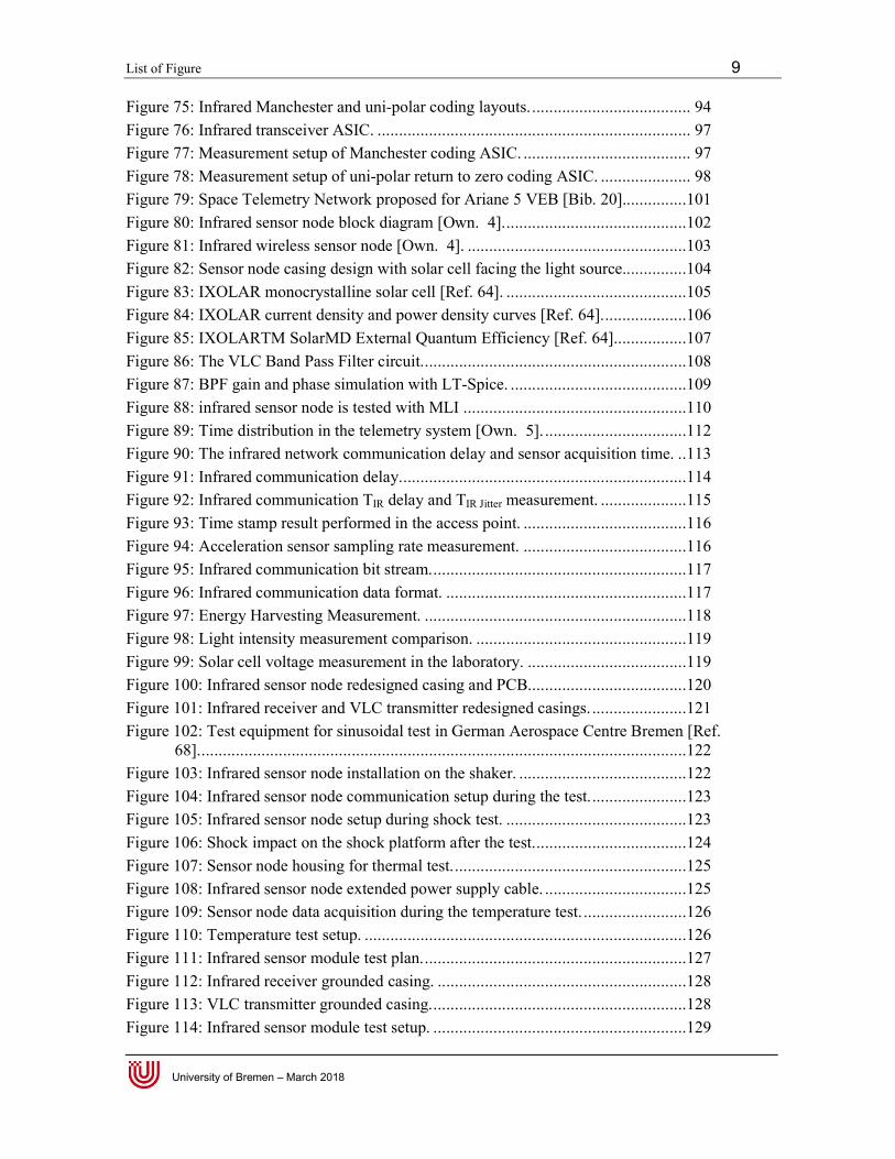
List of Figure 7
University of Bremen – March 2018
List of Figure Figure 1: Versatile analog mixed signal sensor module design constraints. ................. 15 Figure 2: The wireless sensor node placement for Ariane 5 upper stage [Ref. 3]. ........ 17 Figure 3: Example of space vehicle harness integration on ATV-2 “Johannes Kepler” [Ref. 5].
........................................................................................................................ 18 Figure 4: The wireless sensor network in the Vehicle Equipment Bay that is built with sensor
modules developed in the frame of this work [Ref. 6]. ..................................... 18 Figure 5: MicroWIS-based physical view [Ref. 81]. .................................................... 19 Figure 6: Ariane 5 launch sequence at Guiana Space Centre [Ref. 3]. ......................... 22 Figure 7: Typical longitudinal static acceleration during flight [Ref. 3]. ...................... 24 Figure 8: Sinusoidal vibration at the spacecraft base [Ref. 3]. ..................................... 24 Figure 9: Acoustic Vibration Spectrum [Ref. 3]. ......................................................... 25 Figure 10: Envelope shock spectrum for state separation and fairing separation [Ref. 3].26 Figure 11: Variation of static pressure inside the fairing compartment [Ref. 3]. .......... 27 Figure 12: Aerothermal fluxes on trajectory after fairing separation [Ref. 3]. .............. 28 Figure 13: The electromagnetic radiation/emission requirements [Ref. 3]. .................. 29 Figure 14: ECSS Sensor Module Development Flow [Ref. 1]. .................................... 31 Figure 15: Example of UWB transceiver architecture [Bib. 1]. .................................... 35 Figure 16: UWB Electromagnetic radiation measurement under the FCC limits [Bib. 4]. 36 Figure 17: Example of infrared transceiver architecture [Ref. 9]. ................................ 37 Figure 18: P2110-EVAL-01 RF Energy Harvesting Development Kit [Ref. 13]. ......... 38 Figure 19: TE-CORE Thermo Harvesting Power Module [Ref. 15]. ........................... 39 Figure 20: Protection layer of commercial piezoelectric element [Ref. 17]. ................. 40 Figure 21: A typical piezoelectric element installation on a holder [Ref. 18]. .............. 40 Figure 22: Solar cell efficiency graph [Ref. 21]. .......................................................... 41 Figure 23: The World’s first energy harvesting iBeacon [Ref. 22]. .............................. 42 Figure 24: Solar Cell Technology Overview [Ref. 24]. ............................................... 43 Figure 25: Vishay Semiconductors's infrared transceiver dimension [Ref. 28]. ............ 48 Figure 26: Classification of simple infrared links according to the degree of directionality of
the transmitter and receiver [Bib. 6]. ................................................................ 48 Figure 27: Basic construction of infrared receiver [Bib. 6]. ......................................... 50 Figure 28: LOS field of view [Bib. 6]. ........................................................................ 51 Figure 29: Non LOS field of view that increases the transmitter radiant intensity Ro[Bib. 6].
........................................................................................................................ 52 Figure 30: The first Visible Light Communication experiment in Japan [Ref. 29]. ...... 53 Figure 31: Frequency response of the typical solar cell [Bib. 8]. ................................. 54 Figure 32: Space qualified temperature sensor [Ref. 32]. ............................................ 57 Figure 33: Space qualified acceleration sensor [Ref. 33]. ............................................ 57 Figure 34: Space qualified absolute pressure sensor [Ref. 35]. .................................... 58 Figure 35: SHT11 internal block diagram [Ref. 38]. ................................................... 59 Figure 36: SHT11 relative humidity sensor [Ref. 38]. ................................................. 60

List of Figure 8
University of Bremen – March 2018
Figure 37: Pressure sensor MS5534A internal block diagram [Ref. 40]. ...................... 60 Figure 38: MS5534A pressure sensor dimension [Ref. 40]. ......................................... 61 Figure 39: Three axis acceleration sensor ADXL345 internal block diagram [Ref. 42]. 62 Figure 40: ADXL345 three axis acceleration sensor [Ref. 43]. .................................... 63 Figure 41: Visible and infrared light sensor TSL2560 internal block diagram [Ref. 45].64 Figure 42: TSL2560 visible and infrared light sensor [Ref. 45]. .................................. 64 Figure 43: Appolo 1 command module [Ref. 48]. ....................................................... 66 Figure 44: CNT application on the space material [Bib. 9]. ......................................... 66 Figure 45: MLI stacking arrangement in space shuttle Columbia [Ref. 49]. ................. 67 Figure 46: MLI physical view for cryognic hydrogen tanks [Ref. 50]. ......................... 68 Figure 47: MLI microscopic surface structure [Ref. 50]. ............................................. 69 Figure 48: Infrared Absorptance measurement on MLI [Ref. 50]. ............................... 70 Figure 49: Common MLI materials used: a) 10 layers, b) 20 layers. ............................ 70 Figure 50: MLI material on the VEB [Ref. 4]. ............................................................. 71 Figure 51: Experiment setup with MLI material. ......................................................... 72 Figure 52: The infrared transceiver schematic with pattern generator and current source.73 Figure 53: Unknown probability function of the experiment. ...................................... 74 Figure 54: Bit-error-rate (BER) measurement versus LED resistance in different illumination
conditions [Own. 2] ........................................................................................ 74 Figure 55: LED radiant intensity vs. forward current [Ref. 10]. ................................... 75 Figure 56: Bit-error-rate (BER) measurement results with infrared transceiver angle variation
[Own. 2] .......................................................................................................... 76 Figure 57: Infrared LED's propagation pattern [Ref. 10]. ............................................ 77 Figure 58: Infrared receiver gain pattern [Ref. 9]. ....................................................... 77 Figure 59: Manchester coding signal representation [Ref. 51]. .................................... 78 Figure 60: Pulse distance coding signal representation [Ref. 51]. ................................ 79 Figure 61: Pulse length coding signal representation [Ref. 51]. ................................... 79 Figure 62: Manchester coding and uni-polar return to zero spectral density comparison [Bib.
15]. .................................................................................................................. 81 Figure 63: Manchester and uni-polar return to zero spectral density simulation [Own. 3]. 83 Figure 64: Manchester coding transmitter and receiver block diagram. ....................... 85 Figure 65: Manchester transmitter and receiver simulation. ......................................... 86 Figure 66: FPGA prototype for testing the modulation methods. ................................. 86 Figure 67: Manchester coding infrared transceiver signal. ........................................... 87 Figure 68: Manchester recovered UART signal at the FPGA output. ........................... 88 Figure 69: The uni-polar return to zero coding transmitter and receiver block diagram.89 Figure 70: Uni-polar return to zero transmitter and receiver simulation. ...................... 89 Figure 71: Uni-polar return to zero coding infrared transceiver signal. ........................ 90 Figure 72: Uni-polar return to zero recovered UART signal at the FPGA output. ........ 91 Figure 73: Astabile multivibrator circuit for 3/16 pulse recovery block. ...................... 91 Figure 74: Astabile multivibrator circuit simulation. ................................................... 92
List of Figure 9
University of Bremen – March 2018
Figure 75: Infrared Manchester and uni-polar coding layouts. ..................................... 94 Figure 76: Infrared transceiver ASIC. ......................................................................... 97 Figure 77: Measurement setup of Manchester coding ASIC. ....................................... 97 Figure 78: Measurement setup of uni-polar return to zero coding ASIC. ..................... 98 Figure 79: Space Telemetry Network proposed for Ariane 5 VEB [Bib. 20]...............101 Figure 80: Infrared sensor node block diagram [Own. 4]. ..........................................102 Figure 81: Infrared wireless sensor node [Own. 4]. ...................................................103 Figure 82: Sensor node casing design with solar cell facing the light source...............104 Figure 83: IXOLAR monocrystalline solar cell [Ref. 64]. ..........................................105 Figure 84: IXOLAR current density and power density curves [Ref. 64]. ...................106 Figure 85: IXOLARTM SolarMD External Quantum Efficiency [Ref. 64]. ................107 Figure 86: The VLC Band Pass Filter circuit. .............................................................108 Figure 87: BPF gain and phase simulation with LT-Spice. .........................................109 Figure 88: infrared sensor node is tested with MLI . ...................................................110 Figure 89: Time distribution in the telemetry system [Own. 5]. .................................112 Figure 90: The infrared network communication delay and sensor acquisition time. ..113 Figure 91: Infrared communication delay. ..................................................................114 Figure 92: Infrared communication TIR delay and TIR Jitter measurement. ....................115 Figure 93: Time stamp result performed in the access point. ......................................116 Figure 94: Acceleration sensor sampling rate measurement. ......................................116 Figure 95: Infrared communication bit stream. ...........................................................117 Figure 96: Infrared communication data format. ........................................................117 Figure 97: Energy Harvesting Measurement. .............................................................118 Figure 98: Light intensity measurement comparison. .................................................119 Figure 99: Solar cell voltage measurement in the laboratory. .....................................119 Figure 100: Infrared sensor node redesigned casing and PCB. ....................................120 Figure 101: Infrared receiver and VLC transmitter redesigned casings. ......................121 Figure 102: Test equipment for sinusoidal test in German Aerospace Centre Bremen [Ref.
68]. .................................................................................................................122 Figure 103: Infrared sensor node installation on the shaker. .......................................122 Figure 104: Infrared sensor node communication setup during the test. ......................123 Figure 105: Infrared sensor node setup during shock test. ..........................................123 Figure 106: Shock impact on the shock platform after the test. ...................................124 Figure 107: Sensor node housing for thermal test. ......................................................125 Figure 108: Infrared sensor node extended power supply cable. .................................125 Figure 109: Sensor node data acquisition during the temperature test. ........................126 Figure 110: Temperature test setup. ...........................................................................126 Figure 111: Infrared sensor module test plan. .............................................................127 Figure 112: Infrared receiver grounded casing. ..........................................................128 Figure 113: VLC transmitter grounded casing. ...........................................................128 Figure 114: Infrared sensor module test setup. ...........................................................129

List of Figure 10
University of Bremen – March 2018
Figure 115: Uosat-3 localization of errors on earth orbit [Ref. 69]. .............................130 Figure 116: Particle interaction of space particle with a transistor [Bib. 21]. ..............133 Figure 117: Illustration of perfectly elastic and inelastic collisions [Ref. 72]. .............133 Figure 118: Proton stopping power for low- and high-Z materials [Ref. 73]. ..............134 Figure 119: Optical wireless sensor node for space [Bib. 26]. ....................................135 Figure 120: Threshold voltage shift of an NMOS (a) and PMOS (b) transistor vs. accumulated
dose [Bib. 43]. ................................................................................................138 Figure 121: Positive charged particles trapped into the "bird's beak" region [Bib. 44].138 Figure 122: Comparison between conventional and radiation hardened layout techniques [Bib.
22]. .................................................................................................................139 Figure 123: Guard rings layout enclosing MOS transistor [Bib. 23]. ..........................140 Figure 124: CMOS Memory Cell Modified with RG Resistors [Bib. 45]....................141 Figure 125: Schematic of a flip flop with two additional PMOS hold transistors [Bib. 46].
.......................................................................................................................142
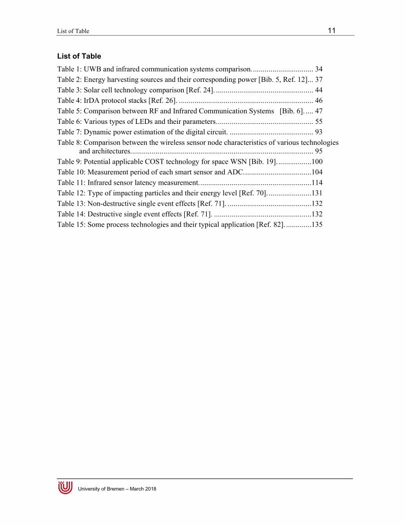
List of Table 11
University of Bremen – March 2018
List of Table Table 1: UWB and infrared communication systems comparison. ............................... 34 Table 2: Energy harvesting sources and their corresponding power [Bib. 5, Ref. 12]. .. 37 Table 3: Solar cell technology comparison [Ref. 24]. .................................................. 44 Table 4: IrDA protocol stacks [Ref. 26]. ..................................................................... 46 Table 5: Comparison between RF and Infrared Communication Systems [Bib. 6]. .... 47 Table 6: Various types of LEDs and their parameters. ................................................. 55 Table 7: Dynamic power estimation of the digital circuit. ........................................... 93 Table 8: Comparison between the wireless sensor node characteristics of various technologies
and architectures. ............................................................................................. 95 Table 9: Potential applicable COST technology for space WSN [Bib. 19]. .................100 Table 10: Measurement period of each smart sensor and ADC. ..................................104 Table 11: Infrared sensor latency measurement. .........................................................114 Table 12: Type of impacting particles and their energy level [Ref. 70]. ......................131 Table 13: Non-destructive single event effects [Ref. 71]. ...........................................132 Table 14: Destructive single event effects [Ref. 71]. ..................................................132 Table 15: Some process technologies and their typical application [Ref. 82]. .............135
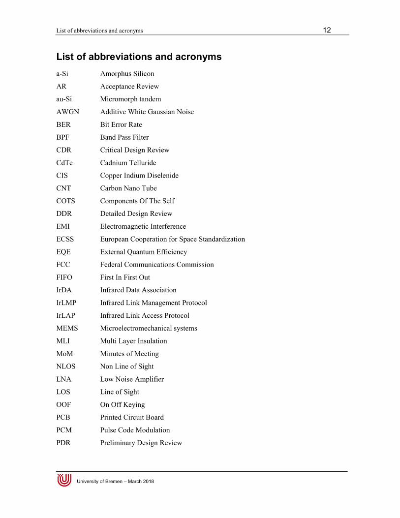
List of abbreviations and acronyms 12
University of Bremen – March 2018
List of abbreviations and acronyms a-Si Amorphus Silicon
AR Acceptance Review
au-Si Micromorph tandem
AWGN Additive White Gaussian Noise
BER Bit Error Rate
BPF Band Pass Filter
CDR Critical Design Review
CdTe Cadnium Telluride
CIS Copper Indium Diselenide
CNT Carbon Nano Tube
COTS Components Of The Self
DDR Detailed Design Review
EMI Electromagnetic Interference
ECSS European Cooperation for Space Standardization
EQE External Quantum Efficiency
FCC Federal Communications Commission
FIFO First In First Out
IrDA Infrared Data Association
IrLMP Infrared Link Management Protocol
IrLAP Infrared Link Access Protocol
MEMS Microelectromechanical systems
MLI Multi Layer Insulation
MoM Minutes of Meeting
NLOS Non Line of Sight
LNA Low Noise Amplifier
LOS Line of Sight
OOF On Off Keying
PCB Printed Circuit Board
PCM Pulse Code Modulation
PDR Preliminary Design Review

List of abbreviations and acronyms 13
University of Bremen – March 2018
PPM Pulse Position Modulation
PSD Power Spectral Density
PROM Programmable Read Only Memory
QR Quality Assurance
RFID Radio Frequency Identification
RTL Register Transfer Logic
RTZ Return to Zero
SEB Single Event Burnout
SED Single Event Disturb
SEDF Single Event Dielectric Failure
SEE Single Event Effects
SEGR Single Event Gate Rupture
SEL Single Event Latchup
SEU Single Event Upset
SES Single Event Snapback
SET Single Event Transient
SID Shock Inducing Device
SRR System Requirement Review
VEB Vehicle Equipment Bay
UWB Ultra Wide Band
1 Introduction 14
University of Bremen – March 2018
1 Introduction The development of space electronics especially for launcher such as Ariane 6 has to fulfill space standards and space requirements provided by the space industries. The standards of the European Cooperation for Space Standardiza-tion (ECSS) are used extensively to ensure a development process that meets the space requirements. This standard covers space project management, space product assurance and space engineering. The ECSS is a cooperative effort of the European Space Agency, national Space Agencies and European Industry Associations for the purpose of developing and maintaining common stan-dards[Ref. 1].
The work presented in this dissertation was carried out to fill the gap of devel-oping wireless sensor network for Ariane launchers [Own. 1]. The development process follows the space requirements that demand the sensor node to survive the environmental condition inside the launcher. This makes the work uniquely compared to commercial wireless sensor network development. The versatile analog mixed signal module proposed in this work consists of infra-red transmitter, VLC receiver, power management, data processing with digi-tal/analog sensor interface unit and solar cell as energy harvester. The signal conditioning circuits that comprise Wheatstone bridge and active filters are also included in the module. The sensor module is used to build wireless sen-sor network inside the Vehicle Equipment Bay (VEB) of Ariane 5.
After the process of development was completed, several measurements were taken to test the sensor module capability to withstand temperature, vibration, shock and Electromagnetic Interference (EMI) given by the Ariane 5 require-ments. These tests are categorized as engineering and are listed as following:
Temperature test Vibration test Shock test
1 Introduction 15
University of Bremen – March 2018
Electromagnetic interference (EMI) test. The requirements for these tests are taken from Ariane 5 user's manual pro-vided by the European Space Agency. The results of the test will be used to ensure higher technological readiness of the sensor module for the launcher [Ref. 2].
The functionality of the sensor module was also studied to support the devel-opment process towards the final products (this shall be done by the space in-dustry).
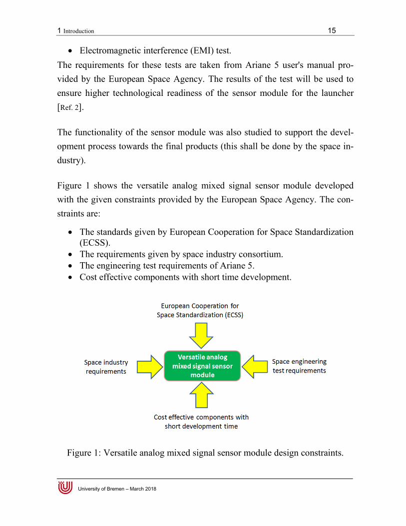
Figure 1 shows the versatile analog mixed signal sensor module developed with the given constraints provided by the European Space Agency. The con-straints are:
The standards given by European Cooperation for Space Standardization (ECSS).
The requirements given by space industry consortium. The engineering test requirements of Ariane 5. Cost effective components with short time development.
Figure 1: Versatile analog mixed signal sensor module design constraints.
1 Introduction 16
University of Bremen – March 2018
At the end, a radiation protection method is proposed in order to reduce the radiation effect caused by space radiation environment.
1.1 The Author’s Contribution Some of the author’s contributions to this work are:
- Development of wireless sensor network for Ariane Launcher especially
used inside Ariane’s 5 vehicle equipment bay (VEB) [Own. 1].
- Studying the impact of the multi layer insulator inside (MLI) the VEB
towards infrared communication profile [Own. 2].
- Development of low power infrared transceiver ASIC with AMS350 nm
technologies [Own. 3].
- Development of time stamp and time synchronization method that utilize
visible light communication to provide clock information concurrently
to all of the sensor nodes [Own. 5].
- Development of infrared sensor node for Ariane 5's telemetry subsystem
with various smart sensors [Own. 4].
- Development of energy harvesting method with visible light communi-
cation (VLC) that utilizes solar cell as receiver [Own. 5].
- Testing the infrared wireless sensor network that meets Ariane 5's re-
quirements [Ref. 3].
- Presenting an overview about the space radiation methods that can be
used to protect the infrared sensor network in future development.
1.2 Goal of developing the analog mixed signal sensor module
The main goal of developing a versatile analog mixed signal sensor module is to reduce the harness inside the launcher by using it as a wireless sensor. The
1 Introduction 17
University of Bremen – March 2018
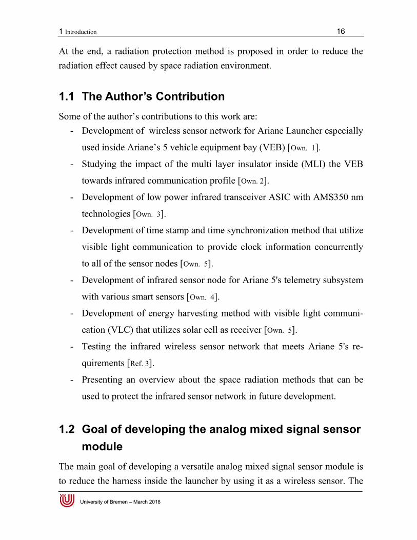
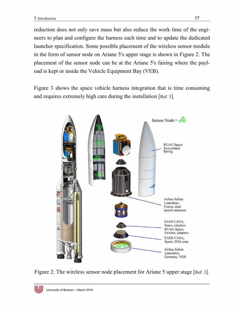
reduction does not only save mass but also reduce the work time of the engi-neers to plan and configure the harness each time and to update the dedicated launcher specification. Some possible placement of the wireless sensor module in the form of sensor node on Ariane 5's upper stage is shown in Figure 2. The placement of the sensor node can be at the Ariane 5's fairing where the payl-oad is kept or inside the Vehicle Equipment Bay (VEB). Figure 3 shows the space vehicle harness integration that is time consuming and requires extremely high care during the installation [Ref. 3].
Figure 2: The wireless sensor node placement for Ariane 5 upper stage [Ref. 3].
1 Introduction 18
University of Bremen – March 2018
The VEB contains the brain of the launch vehicle with on-board computer and it houses most of the electronics for the flight control [Ref. 4]. The implementa-tion of the sensor module in the frame of this work is for building wireless sensor networks that do not show electromagnetic emission that exceeds the limit permitted inside the launch vehicle.
Figure 3: Example of space vehicle harness integration on ATV-2 “Johannes Kepler” [Ref. 5].
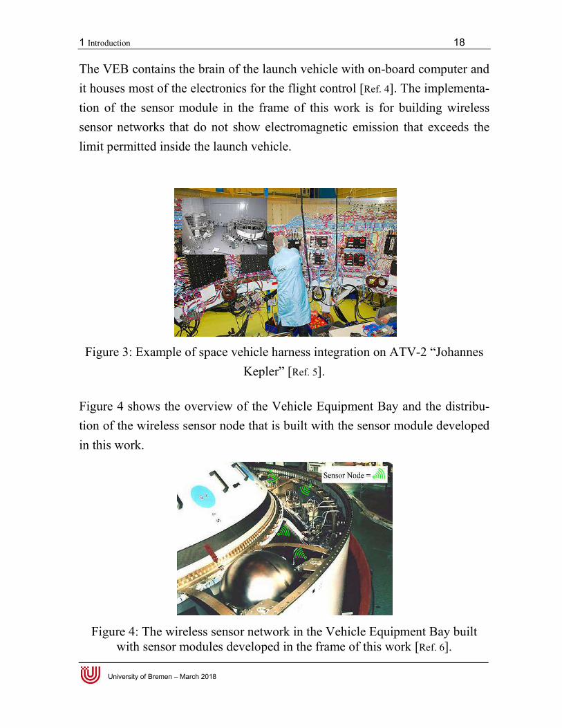
Figure 4 shows the overview of the Vehicle Equipment Bay and the distribu-tion of the wireless sensor node that is built with the sensor module developed in this work.
Figure 4: The wireless sensor network in the Vehicle Equipment Bay built with sensor modules developed in the frame of this work [Ref. 6].
1 Introduction 19
University of Bremen – March 2018
1.3 Wireless Sensor Node Development Overview on Space Application
Since sensor technologies and small scale (micro, nano-scaled technologies) electronics has shown in principle high dynamics in their evolution within a short time, this demands time to market of the product development becoming very fast. This also drives the development of the energy-autonomous sensor node. The development of such sensor has been shown by Swiss Center for Electronics and Microtechnology with WiseNET [Bib. 25] and Smart DUST, that incorporate System on Chip solution with bidirectional optical communi-cation [Bib. 26]. The new architecture that introduces satellite-on-a-chip “Space Chip” was also purpose in [Bib. 24]. Some considerations that shall be taken for designing wireless sensor network for space are discussed extensively in [Bib.
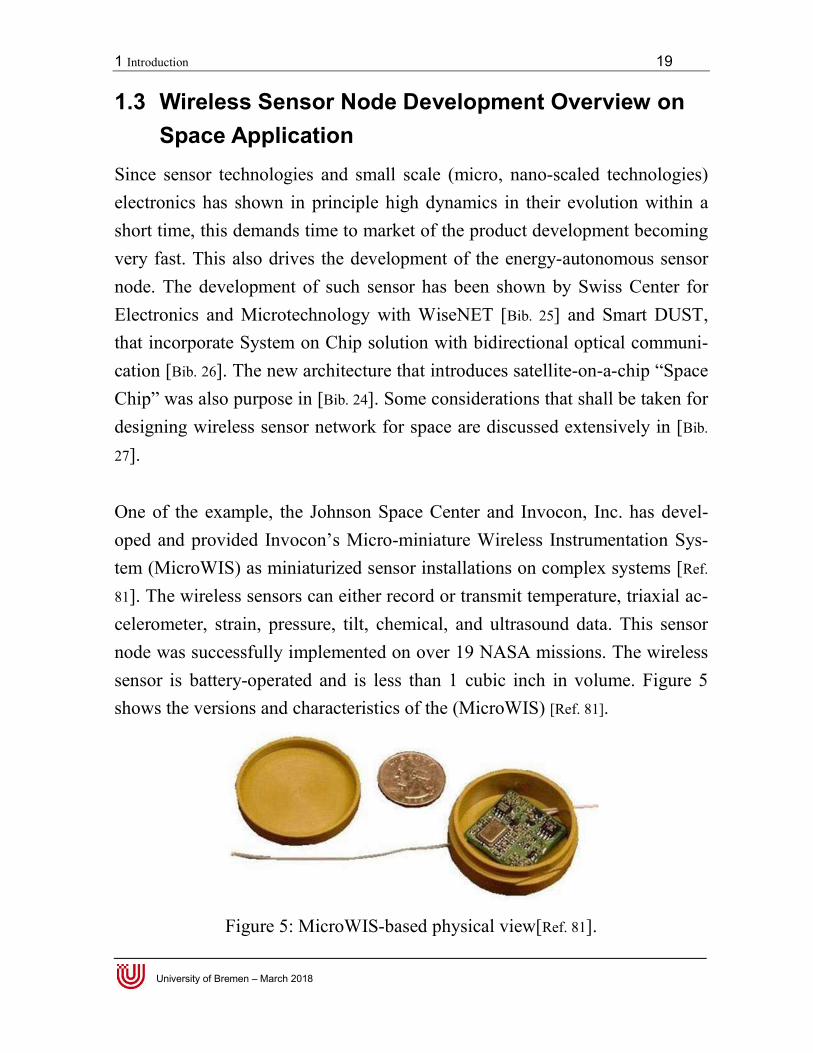
27]. One of the example, the Johnson Space Center and Invocon, Inc. has devel-oped and provided Invocon’s Micro-miniature Wireless Instrumentation Sys-tem (MicroWIS) as miniaturized sensor installations on complex systems [Ref.
81]. The wireless sensors can either record or transmit temperature, triaxial ac-celerometer, strain, pressure, tilt, chemical, and ultrasound data. This sensor node was successfully implemented on over 19 NASA missions. The wireless sensor is battery-operated and is less than 1 cubic inch in volume. Figure 5
shows the versions and characteristics of the (MicroWIS) [Ref. 81].
Figure 5: MicroWIS-based physical view[Ref. 81].
1 Introduction 20
University of Bremen – March 2018
1.4 Objectives Since the development of MicroWIS belongs to a private company such as Invocon, Inc., the know-how to develop such sensor poses challenges for Eu-ropean Space Agency to use similar technology for Ariane launcher [Own. 1]. This leads ESA to develop new sensor node entirely in Europe and the devel-opment processes are reflected in this work. The objectives of developing low power versatile mixed signal sensor module are: Designing sensor module that operates with lower voltage supply (e.g.
3.3V) compared to the current space modules that work with 28 V or 55
V.
Selecting low voltage COTS sensors that are smaller in size and lighter
in comparison with the current space sensors for benchmarking.
Designing reconfigurable interfaces between the COTS sensors and the
data formatting module that allow future COTS sensor products to be
accommodated on the sensor node.
Selecting wireless communication methods that have electromagnetic in-
terference below the given limit provided by the space industry.
Designing wireless charging method that allows the sensor module’s
battery to be fully charged before launching (this is important since the
battery cannot be recharged manually after launcher installation).
Building the prototype of a sensor module that is intended for test and
measurements in the Vehicle Equipment Bay of Ariane 5.
Building the prototype of a sensor module that is intended for engineer-
ing tests against given space requirements.
Purposing a space radiation protection method for sensor modules to
survive the radiation during the mission.
1 Introduction 21
University of Bremen – March 2018
1.5 Structure of the dissertation
The dissertation is divided into several parts covering the development processes starting with general requirements given by the space industry up to the engineering tests to fulfill the space environment requirements. The design methodology is also presented to achieve the best design that fit the given re-quirements. The information is provided in the following chapters: Chapter 2: Wireless Sensor Network System Design
- Selection of Wireless Communication Systems and Energy
Harvesting Methods
- Overview of Space Qualified Sensors and Smart Sensors
- Effect of Space Materials on Infrared Communication
Chapter 3: Infrared Transceiver Design to Optimized Power Con-
sumption
- Selection of Infrared Physical Layer Modulation
- Infrared Transceiver ASIC Design with AMS350 nm
Technology
- Infrared ASIC Test and Power Consumption Measurement
Chapter 4: Infrared Wireless Sensor Node Implementation
- Infrared Wireless Sensor Node Prototype
- Infrared Sensor Node Development
- Infrared Sensor Node Engineering Tests
Chapter 5: Space Radiation Protection Overview
Chapter 6: Summary and Discussion
1 Introduction 22
University of Bremen – March 2018
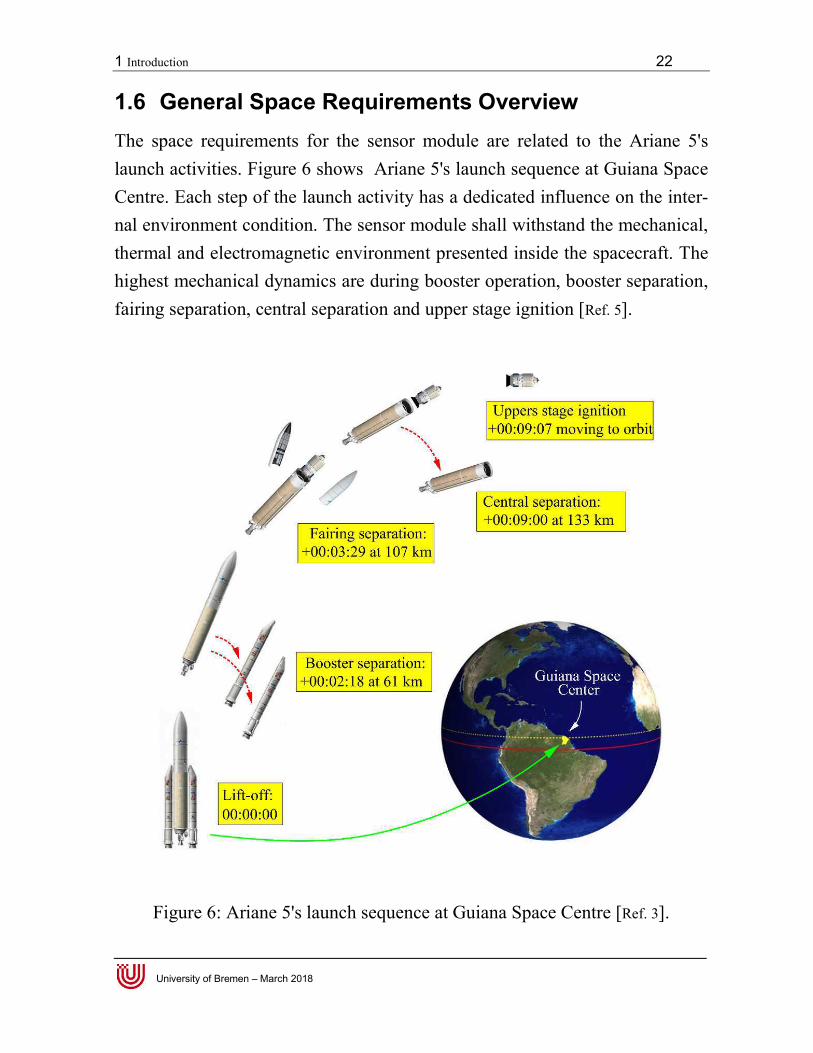
1.6 General Space Requirements Overview The space requirements for the sensor module are related to the Ariane 5's launch activities. Figure 6 shows Ariane 5's launch sequence at Guiana Space Centre. Each step of the launch activity has a dedicated influence on the inter-nal environment condition. The sensor module shall withstand the mechanical, thermal and electromagnetic environment presented inside the spacecraft. The highest mechanical dynamics are during booster operation, booster separation, fairing separation, central separation and upper stage ignition [Ref. 5].
Figure 6: Ariane 5's launch sequence at Guiana Space Centre [Ref. 3].
1 Introduction 23
University of Bremen – March 2018
At typical launch sequence, it is started with the lift-off event. On this event, the twin solid boosters are ignited and the spacecraft is flying with 51.6 de-grees inclination to orbit. The booster separation occurs after 2 minutes and 18 seconds at an altitude of 61 km. The first stage at that time is already ignited and it pushes the upper stage containing the payload to the orbit. At 3 minutes and 29 seconds with an altitude of 107 km, the fairing separation event occurs. The first stage falls after the separation happens at 9 minutes with an altitude of 133 km. 7 second thereafter; the upper stage is ignited and it moves the payload to the orbit. In the following sections, the overview of the space re-quirements are described in relation to launch sequence:
1.6.1 Mechanical environment requirements
The mechanical environment is affected by two factors. The first is the exter-nal factor caused by wind, gust or buffeting at transonic velocity. The second is internal factor caused by the launcher during lift-off, booster separation, fairing separation, central core separation and engine ignitions events.
In Flight Static Acceleration
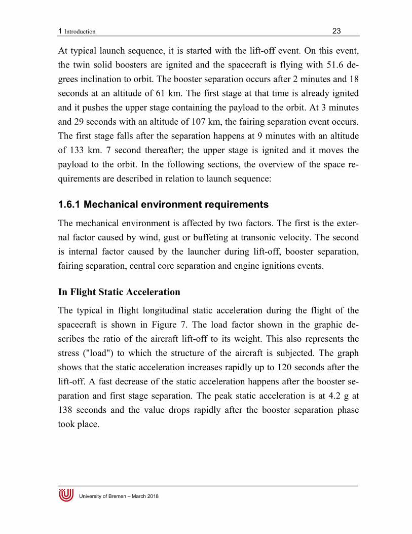
The typical in flight longitudinal static acceleration during the flight of the spacecraft is shown in Figure 7. The load factor shown in the graphic de-scribes the ratio of the aircraft lift-off to its weight. This also represents the stress ("load") to which the structure of the aircraft is subjected. The graph shows that the static acceleration increases rapidly up to 120 seconds after the lift-off. A fast decrease of the static acceleration happens after the booster se-paration and first stage separation. The peak static acceleration is at 4.2 g at 138 seconds and the value drops rapidly after the booster separation phase took place.
1 Introduction
University of Bremen – March 2018
Figure 7: Typical longitudinal static acceleration during flight [
In Flight Sinusoidal Vibration
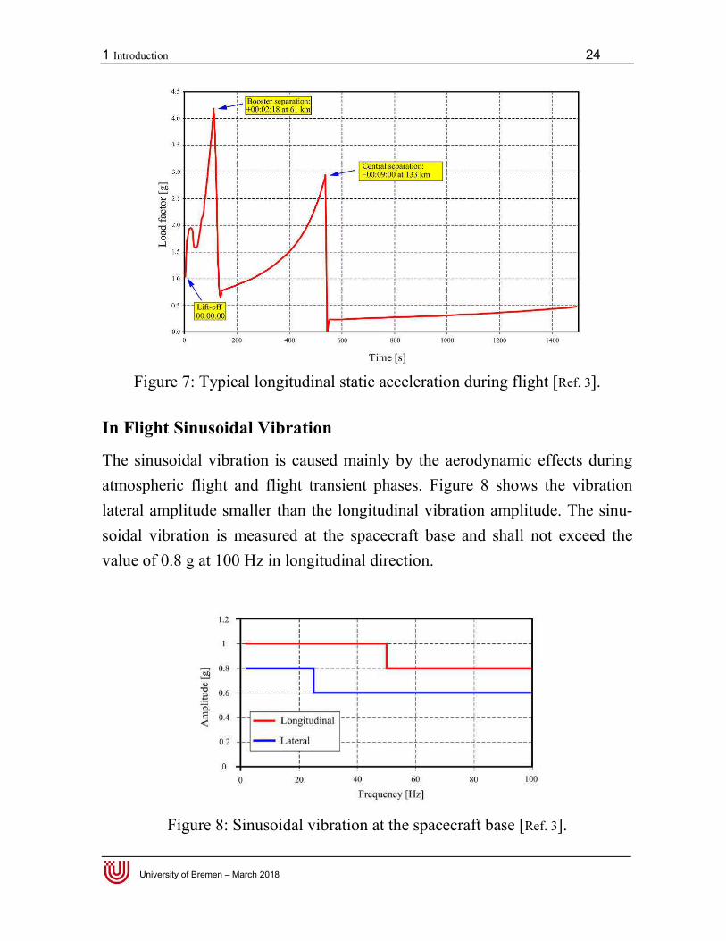
The sinusoidal vibration is caused mainly by the aerodynamic effects during atmospheric flight and flight transient phaseslateral amplitude smaller than the longitudinalsoidal vibration is measured at the spacecraft base and value of 0.8 g at 100 Hz in longitudinal direction.
Figure 8: Sinusoidal vibration at the
: Typical longitudinal static acceleration during flight [
In Flight Sinusoidal Vibration
The sinusoidal vibration is caused mainly by the aerodynamic effects during atmospheric flight and flight transient phases. Figure 8 shows
than the longitudinal vibration amplitude.soidal vibration is measured at the spacecraft base and shall not exceed the value of 0.8 g at 100 Hz in longitudinal direction.
: Sinusoidal vibration at the spacecraft base [Ref.
24
: Typical longitudinal static acceleration during flight [Ref. 3].
The sinusoidal vibration is caused mainly by the aerodynamic effects during shows the vibration
amplitude. The sinu-not exceed the
Ref. 3].
1 Introduction
University of Bremen – March 2018
In Flight Acoustic Vibration
The pressure created by the acoustic vibration is mainly caused by: Plume impingement on the launch pad during lift
Unsteady aerodynamic phenomena during atmospheric flight (e.g. turb
lence inside the boundary layer which is transmitted through the upper
composite structure to the interior of the launcher.
The transonic phase vibration in the range of Mach 0.8 to 1.0 that also
depends on the temperature of the airflow surrounding the spacecraft.
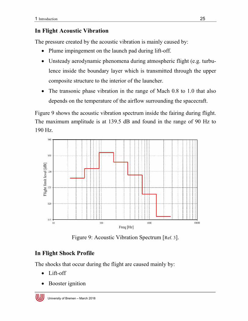
Figure 9 shows the acoustic vibration spectrum inside the fairing during flight. The maximum amplitude is at 139.5 dB and found in the range of190 Hz.
Figure 9: Acoustic Vibration Spectrum [
In Flight Shock Profile
The shocks that occur during the flight are caused mainly by: Lift-off
Booster ignition
In Flight Acoustic Vibration
The pressure created by the acoustic vibration is mainly caused by:Plume impingement on the launch pad during lift-off.
aerodynamic phenomena during atmospheric flight (e.g. turb
lence inside the boundary layer which is transmitted through the upper
composite structure to the interior of the launcher.
The transonic phase vibration in the range of Mach 0.8 to 1.0 that also
depends on the temperature of the airflow surrounding the spacecraft.
shows the acoustic vibration spectrum inside the fairing during flight. The maximum amplitude is at 139.5 dB and found in the range of
: Acoustic Vibration Spectrum [Ref. 3].
The shocks that occur during the flight are caused mainly by:
25
The pressure created by the acoustic vibration is mainly caused by:
aerodynamic phenomena during atmospheric flight (e.g. turbu-
lence inside the boundary layer which is transmitted through the upper
The transonic phase vibration in the range of Mach 0.8 to 1.0 that also
depends on the temperature of the airflow surrounding the spacecraft.
shows the acoustic vibration spectrum inside the fairing during flight. The maximum amplitude is at 139.5 dB and found in the range of 90 Hz to

1 Introduction 26
University of Bremen – March 2018
Booster separation
Fairing separation
Stage separation
The shock spectrum of the stage separation and fairing separation can reach 2000 g in the frequency range of 1 kHz up to 10 kHz (see Figure 10). The stage separation shock is mostly generated at the spacecraft base. The level of the shock for the payload is depending directly on the adapter type, interface diameter and the separation system.
Figure 10: Envelope shock spectrum for state separation and fairing separation [Ref. 3].
1.6.2 In Flight Pressure Requirement
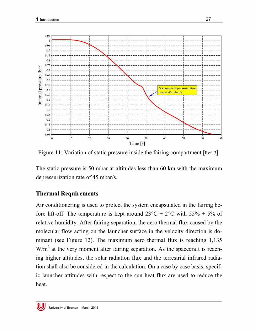
In order to ensure low depressurization rate in the fairing compartment to one way vent doors are utilized. This system ensures the depressurization rate not exceed 2.0 kPa/s that is equal to 20 mbar/s. Figure 11 shows the variation of static pressure inside the fairing compartment.
1 Introduction 27
University of Bremen – March 2018
Figure 11: Variation of static pressure inside the fairing compartment [Ref. 3].
The static pressure is 50 mbar at altitudes less than 60 km with the maximum depressurization rate of 45 mbar/s.
Thermal Requirements
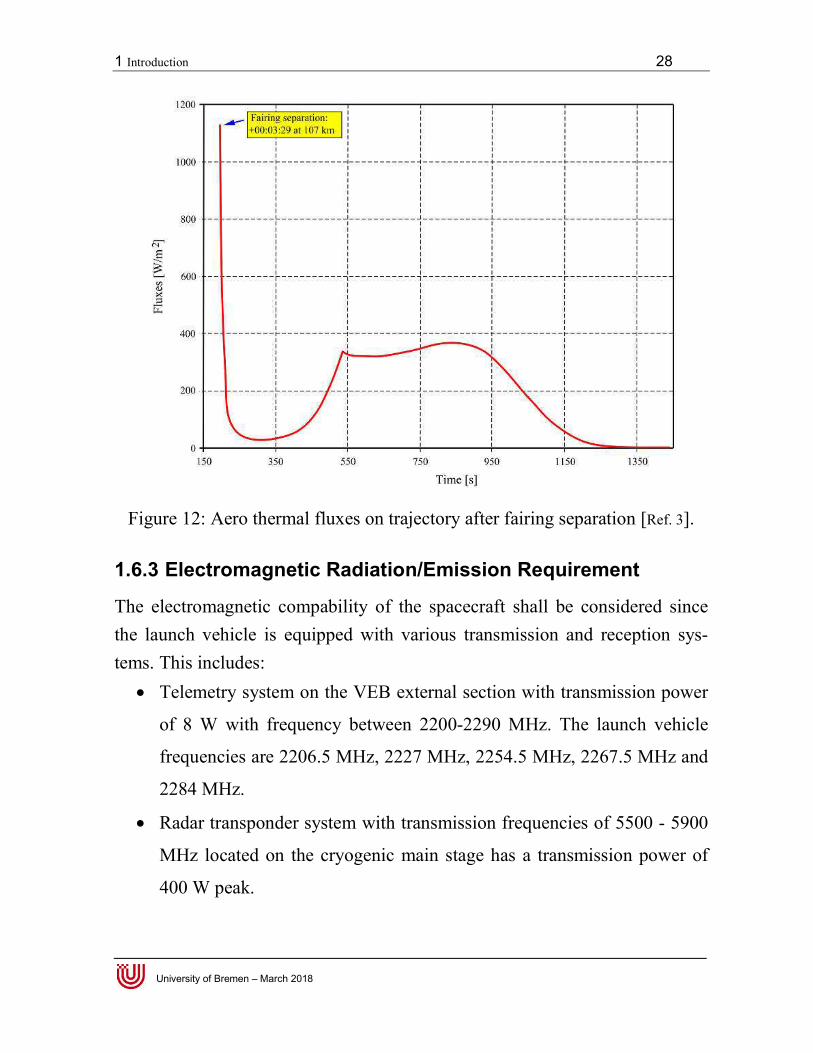
Air conditionering is used to protect the system encapsulated in the fairing be-fore lift-off. The temperature is kept around 23°C ± 2°C with 55% ± 5% of relative humidity. After fairing separation, the aero thermal flux caused by the molecular flow acting on the launcher surface in the velocity direction is do-minant (see Figure 12). The maximum aero thermal flux is reaching 1,135 W/m2 at the very moment after fairing separation. As the spacecraft is reach-ing higher altitudes, the solar radiation flux and the terrestrial infrared radia-tion shall also be considered in the calculation. On a case by case basis, specif-ic launcher attitudes with respect to the sun heat flux are used to reduce the heat.
1 Introduction 28
University of Bremen – March 2018
Figure 12: Aero thermal fluxes on trajectory after fairing separation [Ref. 3].
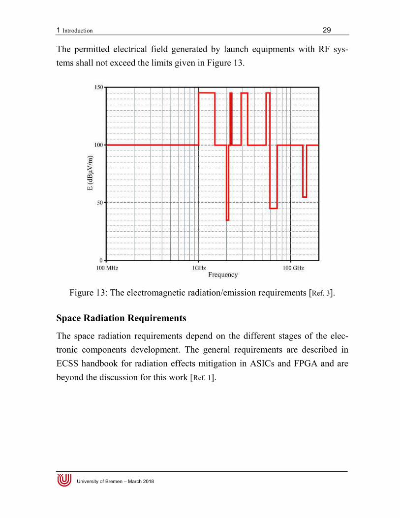
1.6.3 Electromagnetic Radiation/Emission Requirement
The electromagnetic compability of the spacecraft shall be considered since the launch vehicle is equipped with various transmission and reception sys-tems. This includes: Telemetry system on the VEB external section with transmission power
of 8 W with frequency between 2200-2290 MHz. The launch vehicle
frequencies are 2206.5 MHz, 2227 MHz, 2254.5 MHz, 2267.5 MHz and
2284 MHz.
Radar transponder system with transmission frequencies of 5500 - 5900
MHz located on the cryogenic main stage has a transmission power of
400 W peak.
1 Introduction 29
University of Bremen – March 2018
The permitted electrical field generated by launch equipments with RF sys-tems shall not exceed the limits given in Figure 13.
Figure 13: The electromagnetic radiation/emission requirements [Ref. 3].
Space Radiation Requirements
The space radiation requirements depend on the different stages of the elec-tronic components development. The general requirements are described in ECSS handbook for radiation effects mitigation in ASICs and FPGA and are beyond the discussion for this work [Ref. 1].

1 Introduction 30
University of Bremen – March 2018
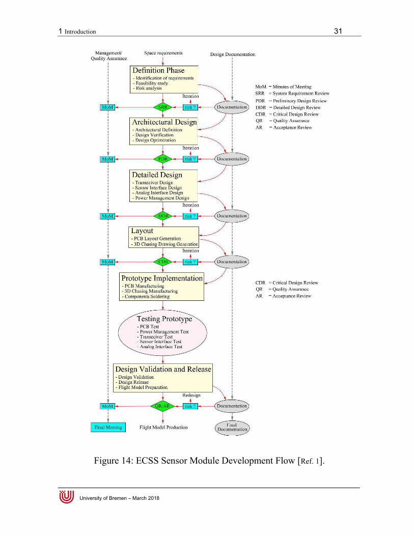
1.7 Design Flow According to the ECSS Standards In this section the design flow of the sensor module development is described according to the ECSS standards [Ref. 1]. The design flow guides the develop-ment process to fulfill the requirements provided by the ESA.
1.7.1 ECSS Sensor Module Development Flow
The design methodology comprises seven main phases (Figure 14). These phases are: Definition phase
Architectural design
Detailed design
Layout
Prototype implementation
Design validation and release
In the Definition phase, the requirements are identified. The feasibility of ful-filling the requirements is studied and the development risk of the design is analyzed. The system requirement review (SRR) is performed before moving to the next phase. The architectural design that comprises of architectural definition, and de-sign verification is required in the second phase. The preliminary design re-view (PDR) will be held for quality assurance. For the Detailed design, the sensor module design was divided in four parts. These are transceiver design, sensor interface design, analog interface design and power management design. At the end of this phase, the detailed design review was conducted.
1 Introduction 31
University of Bremen – March 2018
Figure 14: ECSS Sensor Module Development Flow [Ref. 1].

1 Introduction 32
University of Bremen – March 2018
The PCB layout is generated and a 3D drawing for the sensor module casing is created. This activity is carried out in the Layout phase. The critical design review (CDR) has to be successfully planed before building the prototype. The soldering of the components after manufacturing the PCB and 3D casing shall follow the design in the layout phase. In the Prototype implementation phase, the manufactured parts are tested. This includes PCB test, power man-agement test, transceiver test, sensor interface test and analog interface test. The flight model preparation is ready if the design is validated. Before the flight model is manufactured, the Quality assurance Review (QR) and the ac-ceptance review (AR) shall be performed. Implementation of the ECSS standard for the sensor module design flow will be described in the next sections.
2 Wireless Sensor Network System Design 33
University of Bremen – March 2018
2 Wireless Sensor Network System Design The design of the wireless sensor network system is described in this chapter and is separated in three sections. They are mainly: Selection of Wireless Communication Systems and Energy Harvesting
Methods
Space Qualified and Smart Sensor Overview
Effect of Space Materials on Infrared Communication
2.1 Selection of Wireless Communication Systems and Energy Harvesting Methods
The selection of wireless communication and energy harvesting methods are closely related to the electromagnetic radiation requirements as described in section 2.4. The overview of the commercial wireless communication and wireless energy transfer/harvesting methods are described as following:
2.1.1 Commercial Wireless Communication Overview
Some factors that should be considered to select wireless communication sys-tems for designing the sensor module that meets the electromagnetic require-ments described in section 2.4 are related to: Electromagnetic radiation limit
Communication speed
Communication distance
Power consumption
After considering the factors mentioned above, two communication systems have been selected and are evaluated. They are: short range radio frequency communication system (less EMI) and optical communication system. This is
2 Wireless Sensor Network System Design 34
University of Bremen – March 2018
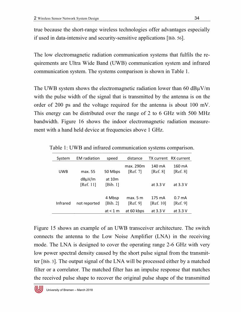
true because the short-range wireless technologies offer advantages especially if used in data-intensive and security-sensitive applications [Bib. 56]. The low electromagnetic radiation communication systems that fulfils the re-quirements are Ultra Wide Band (UWB) communication system and infrared communication system. The systems comparison is shown in Table 1. The UWB system shows the electromagnetic radiation lower than 60 dBµV/m with the pulse width of the signal that is transmitted by the antenna is on the order of 200 ps and the voltage required for the antenna is about 100 mV. This energy can be distributed over the range of 2 to 6 GHz with 500 MHz bandwidth. Figure 16 shows the indoor electromagnetic radiation measure-ment with a hand held device at frequencies above 1 GHz.
Table 1: UWB and infrared communication systems comparison.
System EM radiation speed distance TX current RX current
UWB max. 55 50 Mbps max. 290m
[Ref. 7] 140 mA [Ref. 8]
160 mA [Ref. 8]
dBµV/m [Ref. 11]
at 10m [Bib. 1] at 3.3 V at 3.3 V
Infrared not reported 4 Mbsp [Bib. 2]
max. 5 m [Ref. 9]
175 mA [Ref. 10]
0.7 mA [Ref. 9]
at < 1 m at 60 kbps at 3.3 V at 3.3 V
Figure 15 shows an example of an UWB transceiver architecture. The switch connects the antenna to the Low Noise Amplifier (LNA) in the receiving mode. The LNA is designed to cover the operating range 2-6 GHz with very low power spectral density caused by the short pulse signal from the transmit-ter [Bib. 3]. The output signal of the LNA will be processed either by a matched filter or a correlator. The matched filter has an impulse response that matches the received pulse shape to recover the original pulse shape of the transmitted

2 Wireless Sensor Network System Design 35
University of Bremen – March 2018
signal. A correlator is much simpler to build because it consists of a signal multiplicator and integrator [Bib. 1]. An adjustable high-gain threshold circuit is used to recover the original signal. A digital UWB receiver architecture was later introduced to realize Orthogonal Frequency Division Multiplexing (OFDM). The drawback of this method is that the receiver requires two high speed ADCs. If a flash ADC is used, the power consumption of the receiver part can reach 200 mW [Bib. 4]. This prob-lem can be solved in the optical communication system especially with the commercial infrared receiver that is mostly used for home appliances and con-sumes about 3 mW [Ref. 9].
Figure 15: Example of UWB transceiver architecture [Bib. 1].
Figure 17 shows an example of infrared transceiver architecture. The infrared transmitter consists of only one infrared LED that is modulated with on-off-keying (OOF). The transmitter current varies from 1 mA up to 1000 mA [Ref.
10]. The infrared LED has not been reported to generate electromagnetic radia-tion but the coverage area is limited by the transmitter/LED angle. The typical transmission distance is typically 5 meters (at 60 kbps) with transmission an-gle of ±17° [Ref. 9].
2 Wireless Sensor Network System Design 36
University of Bremen – March 2018
The commercial infrared receiver typically consists of built-in PIN diode, tran-simpedance amplifier and a pulse shaping block [Ref. 9]. This type of infrared receiver is embedded in an epoxy package that functions as an infrared optical filter. This is important to reduce the disturbance to the infrared signal from the ambient light.
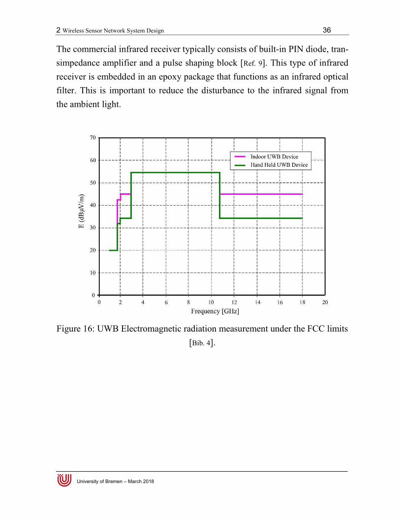
Figure 16: UWB Electromagnetic radiation measurement under the FCC limits [Bib. 4].

2 Wireless Sensor Network System Design 37
University of Bremen – March 2018
Figure 17: Example of infrared transceiver architecture [Ref. 9].
2.1.2 Commercial Energy Harvesting Overview
Other important aspect of realizing a wireless sensor module is the power supply. There are two ways to provide power to the sensor module. The con-ventional way is by using a battery and the other way is by using energy har-vesting elements. Several studies have been conducted to compare the energy harvested in the environment with various energy harvesting elements. The comparison of the power harvested with various energy sources are summa-rized in Table 2. Table 2: Energy harvesting sources and their corresponding power [Bib. 5, Ref.
12]. Energy source Type of source Performance
Light visible light 7500 µW/cm2
Vibration Car engine 100 µW/cm2
RF Wi-Fi 0.001 µW/cm2
GSM 0.1 µW/cm2
Thermal Car exhaust pipe 60 µW/cm2
2 Wireless Sensor Network System Design 38
University of Bremen – March 2018
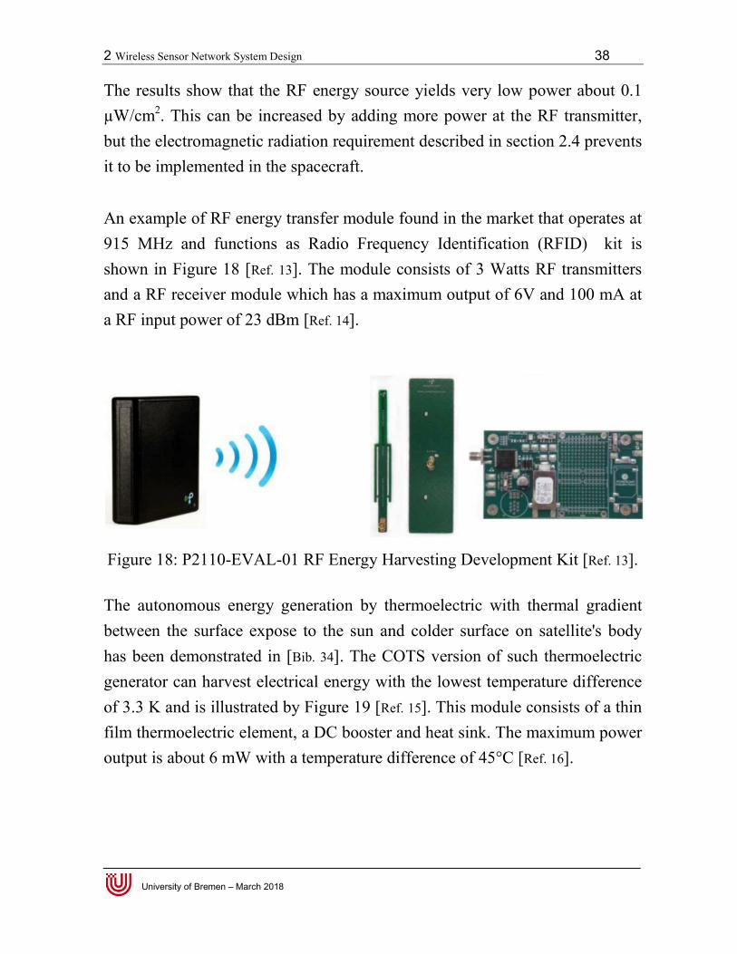
The results show that the RF energy source yields very low power about 0.1 µW/cm2. This can be increased by adding more power at the RF transmitter, but the electromagnetic radiation requirement described in section 2.4 prevents it to be implemented in the spacecraft. An example of RF energy transfer module found in the market that operates at 915 MHz and functions as Radio Frequency Identification (RFID) kit is shown in Figure 18 [Ref. 13]. The module consists of 3 Watts RF transmitters and a RF receiver module which has a maximum output of 6V and 100 mA at a RF input power of 23 dBm [Ref. 14].
Figure 18: P2110-EVAL-01 RF Energy Harvesting Development Kit [Ref. 13].
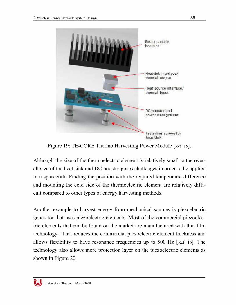
The autonomous energy generation by thermoelectric with thermal gradient between the surface expose to the sun and colder surface on satellite's body has been demonstrated in [Bib. 34]. The COTS version of such thermoelectric generator can harvest electrical energy with the lowest temperature difference of 3.3 K and is illustrated by Figure 19 [Ref. 15]. This module consists of a thin film thermoelectric element, a DC booster and heat sink. The maximum power output is about 6 mW with a temperature difference of 45°C [Ref. 16].
2 Wireless Sensor Network System Design 39
University of Bremen – March 2018
Figure 19: TE-CORE Thermo Harvesting Power Module [Ref. 15].
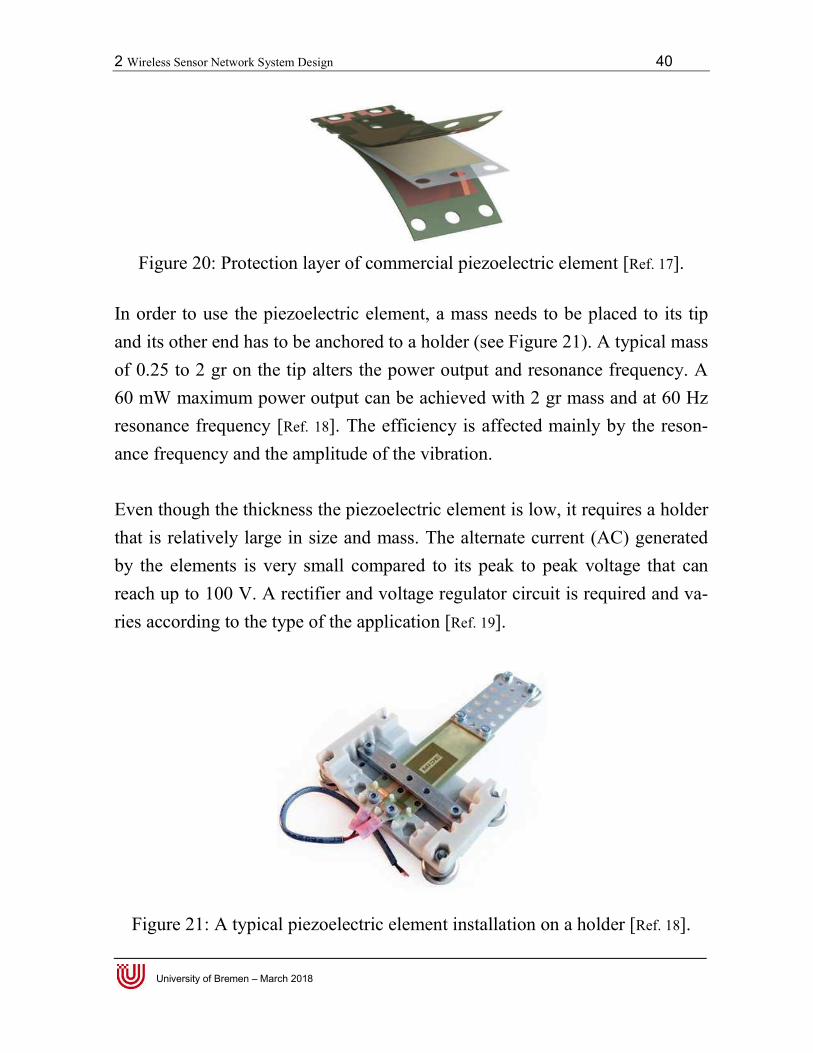
Although the size of the thermoelectric element is relatively small to the over-all size of the heat sink and DC booster poses challenges in order to be applied in a spacecraft. Finding the position with the required temperature difference and mounting the cold side of the thermoelectric element are relatively diffi-cult compared to other types of energy harvesting methods. Another example to harvest energy from mechanical sources is piezoelectric generator that uses piezoelectric elements. Most of the commercial piezoelec-tric elements that can be found on the market are manufactured with thin film technology. That reduces the commercial piezoelectric element thickness and allows flexibility to have resonance frequencies up to 500 Hz [Ref. 16]. The technology also allows more protection layer on the piezoelectric elements as shown in Figure 20.
2 Wireless Sensor Network System Design 40
University of Bremen – March 2018
Figure 20: Protection layer of commercial piezoelectric element [Ref. 17].
In order to use the piezoelectric element, a mass needs to be placed to its tip and its other end has to be anchored to a holder (see Figure 21). A typical mass of 0.25 to 2 gr on the tip alters the power output and resonance frequency. A 60 mW maximum power output can be achieved with 2 gr mass and at 60 Hz resonance frequency [Ref. 18]. The efficiency is affected mainly by the reson-ance frequency and the amplitude of the vibration.
Even though the thickness the piezoelectric element is low, it requires a holder that is relatively large in size and mass. The alternate current (AC) generated by the elements is very small compared to its peak to peak voltage that can reach up to 100 V. A rectifier and voltage regulator circuit is required and va-ries according to the type of the application [Ref. 19].
Figure 21: A typical piezoelectric element installation on a holder [Ref. 18].
2 Wireless Sensor Network System Design 41
University of Bremen – March 2018
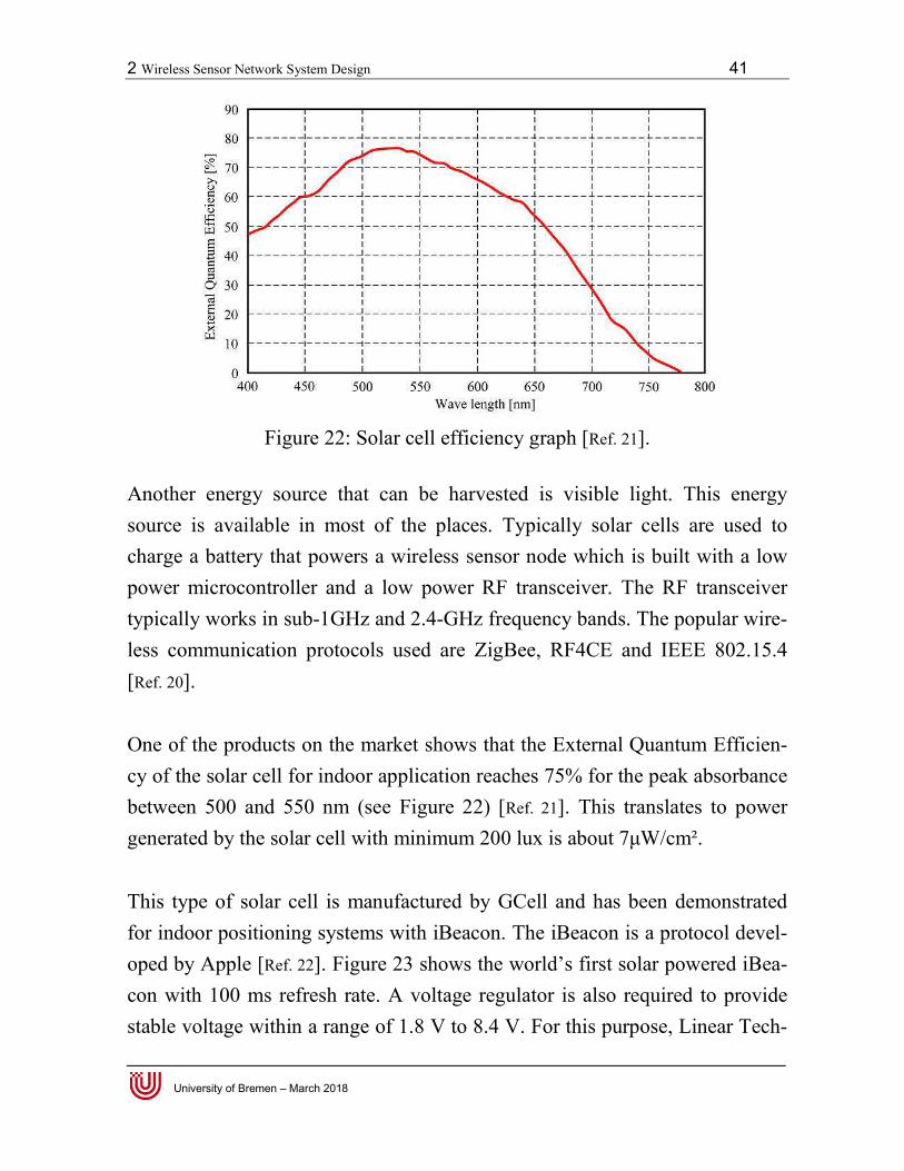
Figure 22: Solar cell efficiency graph [Ref. 21].
Another energy source that can be harvested is visible light. This energy source is available in most of the places. Typically solar cells are used to charge a battery that powers a wireless sensor node which is built with a low power microcontroller and a low power RF transceiver. The RF transceiver typically works in sub-1GHz and 2.4-GHz frequency bands. The popular wire-less communication protocols used are ZigBee, RF4CE and IEEE 802.15.4 [Ref. 20]. One of the products on the market shows that the External Quantum Efficien-cy of the solar cell for indoor application reaches 75% for the peak absorbance between 500 and 550 nm (see Figure 22) [Ref. 21]. This translates to power generated by the solar cell with minimum 200 lux is about 7μW/cm². This type of solar cell is manufactured by GCell and has been demonstrated for indoor positioning systems with iBeacon. The iBeacon is a protocol devel-oped by Apple [Ref. 22]. Figure 23 shows the world’s first solar powered iBea-con with 100 ms refresh rate. A voltage regulator is also required to provide stable voltage within a range of 1.8 V to 8.4 V. For this purpose, Linear Tech-

2 Wireless Sensor Network System Design 42
University of Bremen – March 2018
nology provides a voltage regulator with a minimum operational current of 1.6 µA with an input power of only 7.5 µW [Ref. 23]. Summarizing the commercial energy harvesting alternatives presented above, thermoelectric elements and piezoelectric elements require larger peripherals for an application. The size of the thermoelectric heat sink makes it difficult for installation in narrow places and it is also difficult to locate a heat source inside the spacecraft which shall provide enough temperature difference for a sufficient temperature gradient. The vibration during the launch requires the hot side of the thermoelectric element to be mounted firmly on the spacecraft’s structure. This is difficult since the heat sink is at least ten times larger and heavier than the thermoelectric element. In the case of piezoelectric elements, the mounting method related to the vibration orientation requires much time and effort. Both of these energy harvesting methods are not well suited for wireless energy transfer inside the spacecraft.
Figure 23: The World’s first energy harvesting iBeacon [Ref. 22].
On the other hand the RF and visible light energy harvesting allow energy and information transmission. Unfortunately for the RF case, it is not possible to harvest enough energy inside the spacecraft. This because the transmitter elec-tromagnetic radiation is limited by the requirement described in section 2.4.
2 Wireless Sensor Network System Design 43
University of Bremen – March 2018
As an exemption, the energy transmission through visible light does not vi-olate any of the requirements described in section 2. A solar cell shall be used to receive visible light from a light source positioned in the spacecraft. There are many types of commercial solar cell available which have been de-veloped in recent years. Figure 24 shows an overview of the solar cell tech-nologies that are ranging from thin film technology to organic technology.
There are several parameters to select solar cell for a sensor module. These parameters are [Ref. 24]: Solar cell material
Solar cell efficiency
Power output per surface area
Figure 24: Solar Cell Technology Overview [Ref. 24].
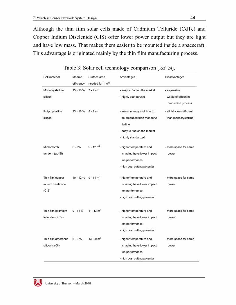
Table 3 shows a comparison of the current technologies available on the mar-ket. Until now, Monocrystalline and polycrystalline silicon deliver the highest power output per surface area [Ref. 24].
2 Wireless Sensor Network System Design 44
University of Bremen – March 2018
Although the thin film solar cells made of Cadmium Telluride (CdTe) and Copper Indium Diselenide (CIS) offer lower power output but they are light and have low mass. That makes them easier to be mounted inside a spacecraft. This advantage is originated mainly by the thin film manufacturing process.
Table 3: Solar cell technology comparison [Ref. 24]. Cell material Module Surface area Advantages Disadvantages
efficiency needed for 1 kW
Monocrystalline 15 - 18 % 7 - 9 m2 - easy to find on the market - expensive
silicon - highly standarized - waste of silicon in
production process
Polycrystalline 13 - 16 % 8 - 9 m2 - lesser energy and time to - slightly less efficient
silicon be produced than monocrys- than monocrystalline
talline
- easy to find on the market
- highly standarized
Micromorph 6 -9 % 9 - 12 m2 - higher temperature and - more space for same
tandem (aμ-Si) shading have lower impact power
on performance
- high cost cutting potential
Thin film copper 10 - 12 % 9 - 11 m2 - higher temperature and - more space for same
indium diselenide shading have lower impact power
(CIS) on performance
- high cost cutting potential
Thin film cadmium 9 - 11 % 11 -13 m2 - higher temperature and - more space for same
telluride (CdTe) shading have lower impact power
on performance
- high cost cutting potential
Thin film amorphus 6 - 8 % 13 -20 m2 - higher temperature and - more space for same
silicon (a-Si) shading have lower impact power
on performance
- high cost cutting potential

2 Wireless Sensor Network System Design 45
University of Bremen – March 2018
After considering many factors and performing commercial wireless commu-nication survey. Also checking the possible commercial energy harvesting technologies, the optical communication method and visible light energy har-vesting and transmission are chosen. This selection is also in line with the re-quirements described in section 2.4. The infrared communication and visible light energy transmission method are described in more detail hereafter:
2.1.3 IrDA Standard and Infrared Communication Link
Before designing an infrared communication system, it is important to under-stand the infrared communication link and infrared standardization. The stan-dardization for commercial infrared communication is drafted by the Infrared Data Association (IrDA). IrDA was founded in 1993 by around 50 companies to specify the protocols for wireless infrared communication that is mostly used for home appliances [Ref. 25]. The IrDA physical layer has three commu-nication speed categories, these are:
Asynchronous Serial IR with 9.6 – 115.2 kbaud, return-to-zero (RTZ)
modulation and reduced original pulse width to 3/16.
Synchronous Serial IR with 1.15 Mbaud, return-to-zero (RTZ) modula-
tion and reduced original pulse width to 1/4.
Synchronous Fast Serial IR with 4 Mbaud and 4 pulse position modula-
tion (PPM).
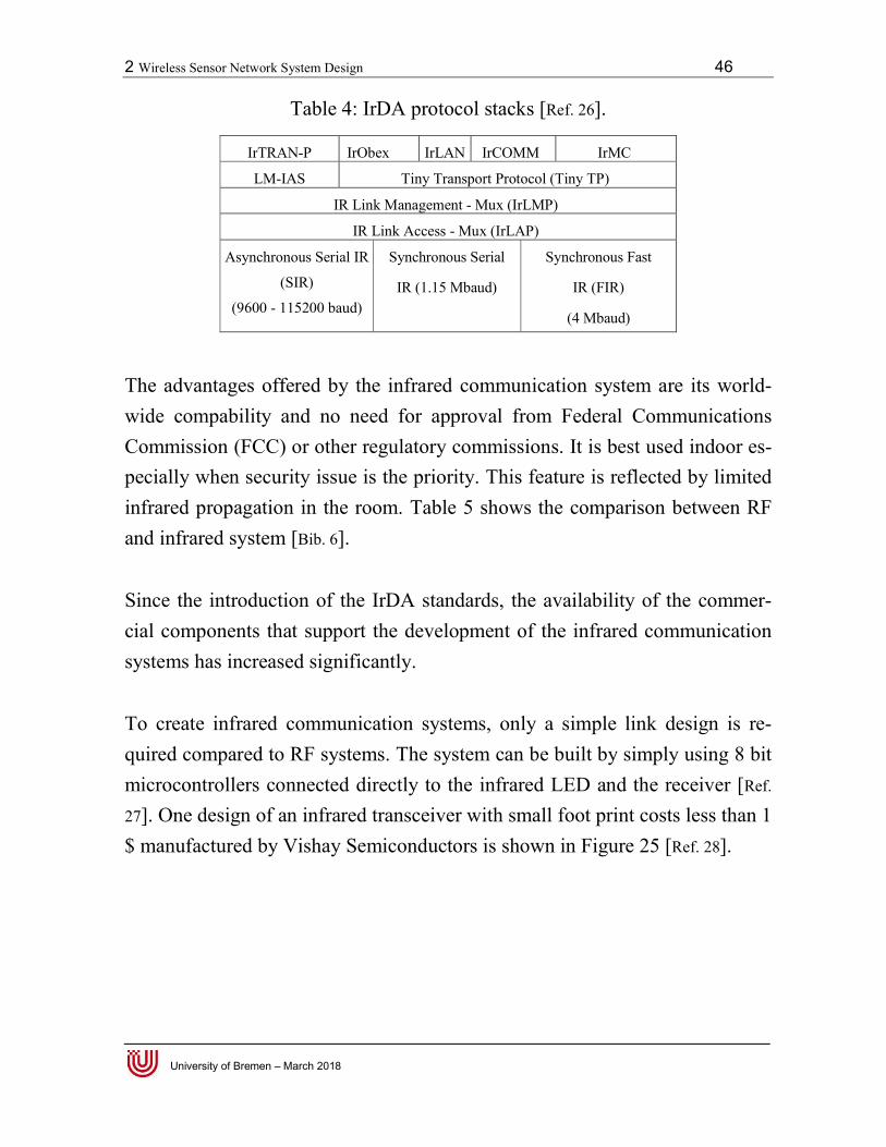
The standard communication range is 1 m with minimum transmission angle of ±15° and the infrared light wavelength is between 850 and 950 nm. On the top of the physical layer are the Link Access Protocol (IrLAP) and Link Man-agement Protocol (IrLMP) some other higher level protocol layers (see Table 4).
2 Wireless Sensor Network System Design 46
University of Bremen – March 2018
Table 4: IrDA protocol stacks [Ref. 26].
IrTRAN-P IrObex IrLAN IrCOMM IrMC
LM-IAS Tiny Transport Protocol (Tiny TP)
IR Link Management - Mux (IrLMP)
IR Link Access - Mux (IrLAP)
Asynchronous Serial IR
(SIR)
(9600 - 115200 baud)
Synchronous Serial
IR (1.15 Mbaud)
Synchronous Fast
IR (FIR)
(4 Mbaud)
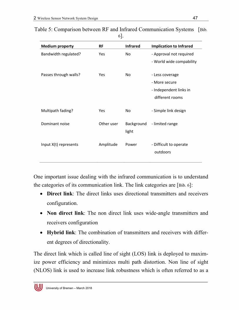
The advantages offered by the infrared communication system are its world-wide compability and no need for approval from Federal Communications Commission (FCC) or other regulatory commissions. It is best used indoor es-pecially when security issue is the priority. This feature is reflected by limited infrared propagation in the room. Table 5 shows the comparison between RF and infrared system [Bib. 6]. Since the introduction of the IrDA standards, the availability of the commer-cial components that support the development of the infrared communication systems has increased significantly. To create infrared communication systems, only a simple link design is re-quired compared to RF systems. The system can be built by simply using 8 bit microcontrollers connected directly to the infrared LED and the receiver [Ref.
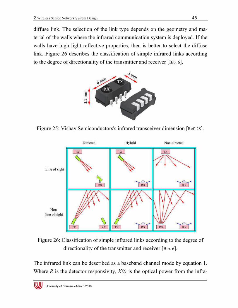
27]. One design of an infrared transceiver with small foot print costs less than 1 $ manufactured by Vishay Semiconductors is shown in Figure 25 [Ref. 28].
2 Wireless Sensor Network System Design 47
University of Bremen – March 2018
Table 5: Comparison between RF and Infrared Communication Systems [Bib. 6].
Medium property RF Infrared Implication to Infrared
Bandwidth regulated? Yes No - Approval not required
- World wide compability
Passes through walls? Yes No - Less coverage
- More secure
- Independent links in
different rooms
Multipath fading? Yes No - Simple link design
Dominant noise Other user Background - limited range
light
Input X(t) represents Amplitude Power - Difficult to operate
outdoors
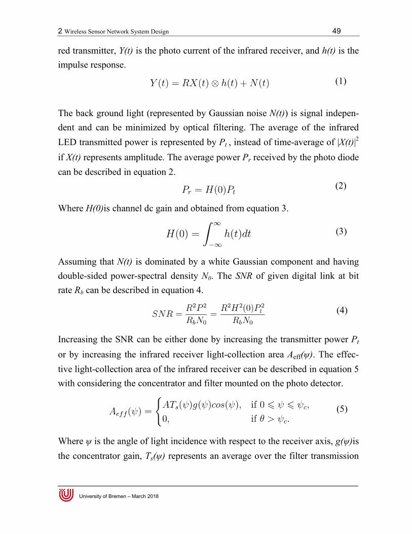
One important issue dealing with the infrared communication is to understand the categories of its communication link. The link categories are [Bib. 6]: Direct link: The direct links uses directional transmitters and receivers
configuration.
Non direct link: The non direct link uses wide-angle transmitters and
receivers configuration
Hybrid link: The combination of transmitters and receivers with differ-
ent degrees of directionality.
The direct link which is called line of sight (LOS) link is deployed to maxim-ize power efficiency and minimizes multi path distortion. Non line of sight (NLOS) link is used to increase link robustness which is often referred to as a
2 Wireless Sensor Network System Design 48
University of Bremen – March 2018
diffuse link. The selection of the link type depends on the geometry and ma-terial of the walls where the infrared communication system is deployed. If the walls have high light reflective properties, then is better to select the diffuse link. Figure 26 describes the classification of simple infrared links according to the degree of directionality of the transmitter and receiver [Bib. 6].
Figure 25: Vishay Semiconductors's infrared transceiver dimension [Ref. 28].
Figure 26: Classification of simple infrared links according to the degree of directionality of the transmitter and receiver [Bib. 6].
The infrared link can be described as a baseband channel mode by equation 1. Where R is the detector responsivity, X(t) is the optical power from the infra-
2 Wireless Sensor Network System Design 49
University of Bremen – March 2018
red transmitter, Y(t) is the photo current of the infrared receiver, and h(t) is the impulse response.
The back ground light (represented by Gaussian noise N(t)) is signal indepen-dent and can be minimized by optical filtering. The average of the infrared LED transmitted power is represented by Pt , instead of time-average of |X(t)|2 if X(t) represents amplitude. The average power Pr received by the photo diode can be described in equation 2.
Where H(0)is channel dc gain and obtained from equation 3.
Assuming that N(t) is dominated by a white Gaussian component and having double-sided power-spectral density N0. The SNR of given digital link at bit rate Rb can be described in equation 4.
Increasing the SNR can be either done by increasing the transmitter power Pt or by increasing the infrared receiver light-collection area Aeff(ψ). The effec-tive light-collection area of the infrared receiver can be described in equation 5 with considering the concentrator and filter mounted on the photo detector.
Where ψ is the angle of light incidence with respect to the receiver axis, g(ψ)is the concentrator gain, Ts(ψ) represents an average over the filter transmission
(1)
(2)
(3)
(4)
(5)
2 Wireless Sensor Network System Design 50
University of Bremen – March 2018
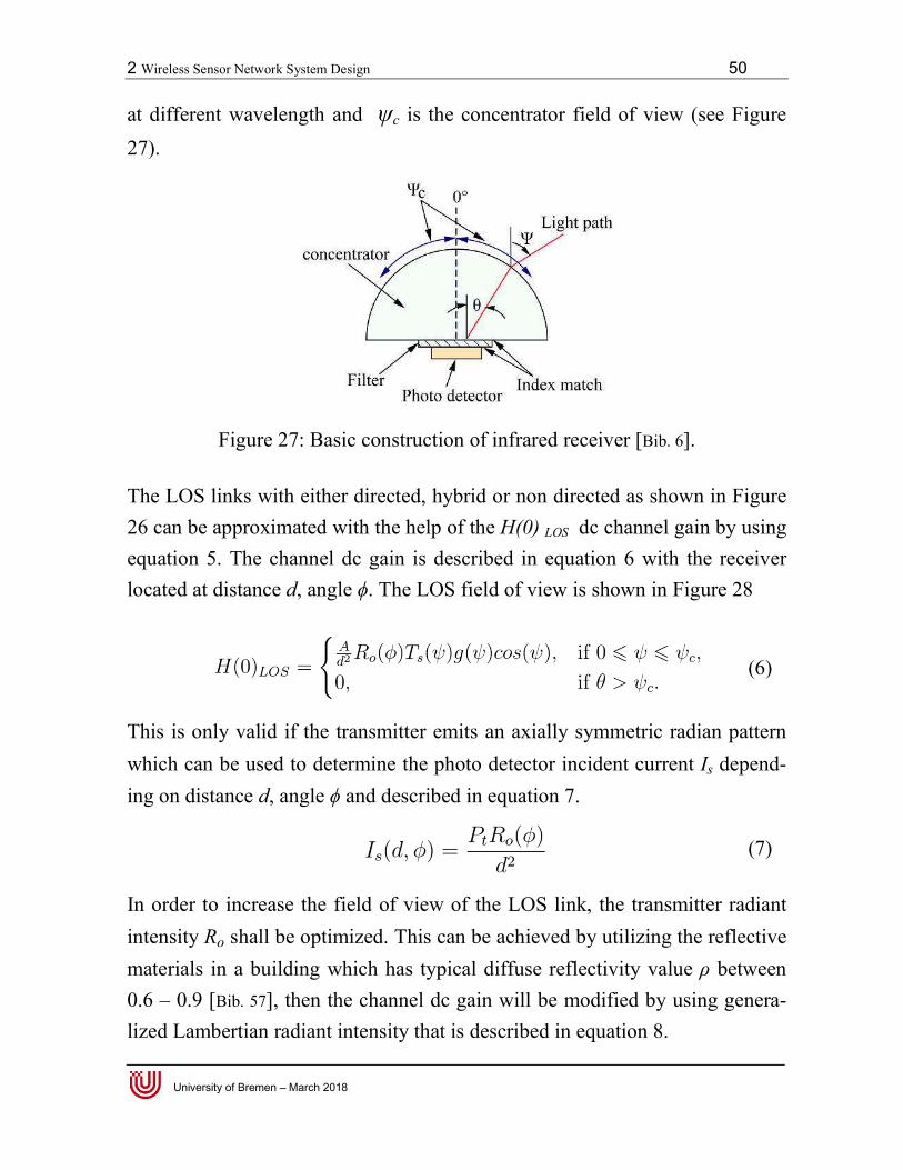
at different wavelength and ψc is the concentrator field of view (see Figure 27).
Figure 27: Basic construction of infrared receiver [Bib. 6].
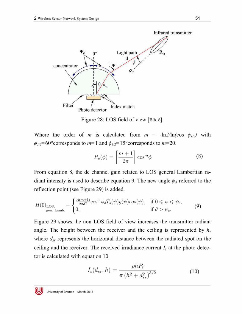
The LOS links with either directed, hybrid or non directed as shown in Figure 26 can be approximated with the help of the H(0) LOS dc channel gain by using equation 5. The channel dc gain is described in equation 6 with the receiver located at distance d, angle ϕ. The LOS field of view is shown in Figure 28
This is only valid if the transmitter emits an axially symmetric radian pattern which can be used to determine the photo detector incident current Is depend-ing on distance d, angle ϕ and described in equation 7.
In order to increase the field of view of the LOS link, the transmitter radiant intensity Ro shall be optimized. This can be achieved by utilizing the reflective materials in a building which has typical diffuse reflectivity value ρ between 0.6 – 0.9 [Bib. 57], then the channel dc gain will be modified by using genera-lized Lambertian radiant intensity that is described in equation 8.
(6)
(7)
2 Wireless Sensor Network System Design 51
University of Bremen – March 2018
Figure 28: LOS field of view [Bib. 6].
Where the order of m is calculated from m = -ln2/ln(cos ϕ1/2) with ϕ1/2=60°corresponds to m=1 and ϕ1/2=15°corresponds to m=20.
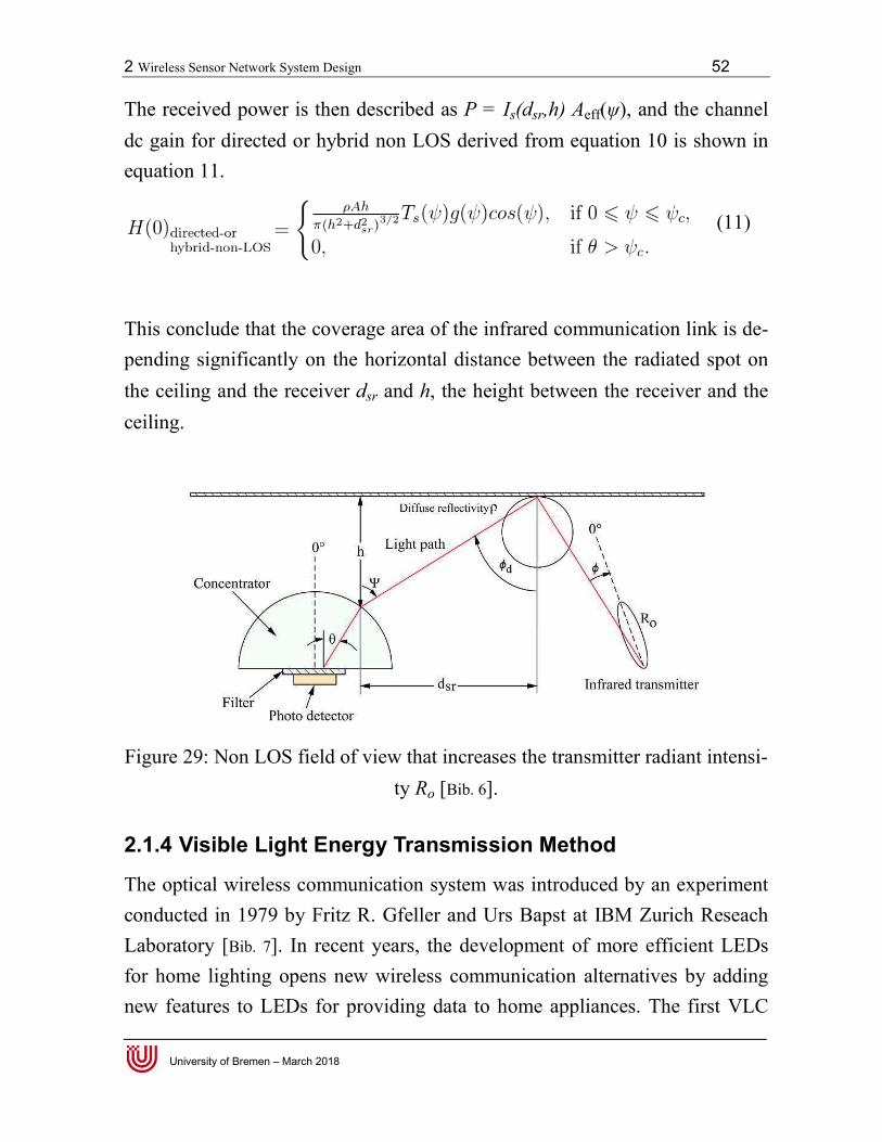
From equation 8, the dc channel gain related to LOS general Lambertian ra-diant intensity is used to describe equation 9. The new angle ϕd referred to the reflection point (see Figure 29) is added.
Figure 29 shows the non LOS field of view increases the transmitter radiant angle. The height between the receiver and the ceiling is represented by h, where dsr represents the horizontal distance between the radiated spot on the ceiling and the receiver. The received irradiance current Is at the photo detec-tor is calculated with equation 10.
(8)
(9)
(10)
2 Wireless Sensor Network System Design 52
University of Bremen – March 2018
The received power is then described as P = Is(dsr,h) Aeff(ψ), and the channel dc gain for directed or hybrid non LOS derived from equation 10 is shown in equation 11.
This conclude that the coverage area of the infrared communication link is de-pending significantly on the horizontal distance between the radiated spot on the ceiling and the receiver dsr and h, the height between the receiver and the ceiling.
Figure 29: Non LOS field of view that increases the transmitter radiant intensi-ty Ro [Bib. 6].
2.1.4 Visible Light Energy Transmission Method
The optical wireless communication system was introduced by an experiment conducted in 1979 by Fritz R. Gfeller and Urs Bapst at IBM Zurich Reseach Laboratory [Bib. 7]. In recent years, the development of more efficient LEDs for home lighting opens new wireless communication alternatives by adding new features to LEDs for providing data to home appliances. The first VLC
(11)
2 Wireless Sensor Network System Design 53
University of Bremen – March 2018
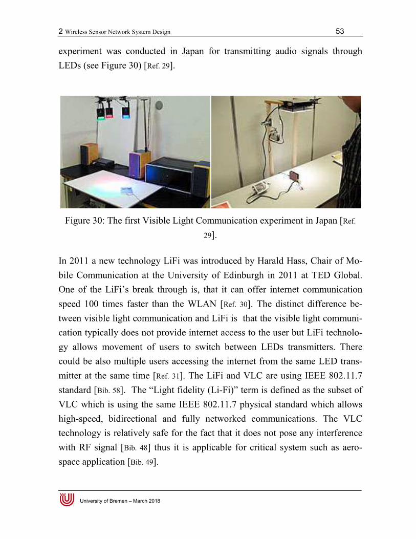
experiment was conducted in Japan for transmitting audio signals through LEDs (see Figure 30) [Ref. 29].
Figure 30: The first Visible Light Communication experiment in Japan [Ref.
29].
In 2011 a new technology LiFi was introduced by Harald Hass, Chair of Mo-bile Communication at the University of Edinburgh in 2011 at TED Global. One of the LiFi’s break through is, that it can offer internet communication speed 100 times faster than the WLAN [Ref. 30]. The distinct difference be-tween visible light communication and LiFi is that the visible light communi-cation typically does not provide internet access to the user but LiFi technolo-gy allows movement of users to switch between LEDs transmitters. There could be also multiple users accessing the internet from the same LED trans-mitter at the same time [Ref. 31]. The LiFi and VLC are using IEEE 802.11.7 standard [Bib. 58]. The “Light fidelity (Li-Fi)” term is defined as the subset of VLC which is using the same IEEE 802.11.7 physical standard which allows high-speed, bidirectional and fully networked communications. The VLC technology is relatively safe for the fact that it does not pose any interference with RF signal [Bib. 48] thus it is applicable for critical system such as aero-space application [Bib. 49].
2 Wireless Sensor Network System Design 54
University of Bremen – March 2018
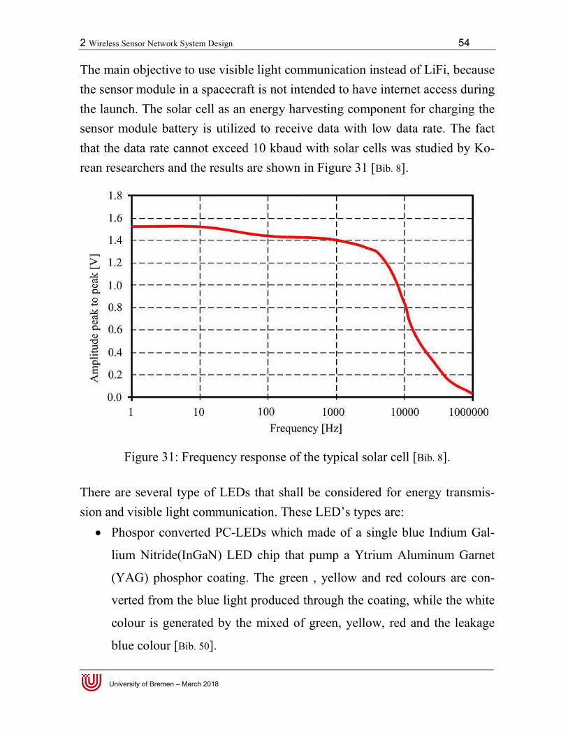
The main objective to use visible light communication instead of LiFi, because the sensor module in a spacecraft is not intended to have internet access during the launch. The solar cell as an energy harvesting component for charging the sensor module battery is utilized to receive data with low data rate. The fact that the data rate cannot exceed 10 kbaud with solar cells was studied by Ko-rean researchers and the results are shown in Figure 31 [Bib. 8].
Figure 31: Frequency response of the typical solar cell [Bib. 8].
There are several type of LEDs that shall be considered for energy transmis-sion and visible light communication. These LED’s types are: Phospor converted PC-LEDs which made of a single blue Indium Gal-
lium Nitride(InGaN) LED chip that pump a Ytrium Aluminum Garnet
(YAG) phosphor coating. The green , yellow and red colours are con-
verted from the blue light produced through the coating, while the white
colour is generated by the mixed of green, yellow, red and the leakage
blue colour [Bib. 50].
2 Wireless Sensor Network System Design 55
University of Bremen – March 2018
The multi chip LEDs are made of combination of 3 or more LED chips
which produce red, green, blue (RGB) color to created white color when
they are mixed.
The organic LEDs (OLED) are made of organic sandwiched layers with
positive and negative carriers. The drawback of this technology is its
low frequency response and mean while offering longer life time (≈
50000 hours) compare with inorganic LEDs [Bib. 51–Bib. 54].
Micro LEDs (μ-LED) consist of micro LED arrays and are made of Al-
GaN. This technology offer high density LEDs with minimum pixel size
of 14-84 μm [Bib. 55].
Table 6 summarizes the LED’s types with various parameters. The LEDs used in this work is a type of OLED that emits up to 4000 lux/m2 at a distance of 1 meter and consumes less than 3 W.
Table 6: Various types of LEDs and their parameters. Parameter pc-LED RGB LED µ-LED OLED Bandwidth 3-5 MHz 10-20 MHz ≥300 MHz ≤1 MHz Efficiency 130 lm/W 65 lm/W N/A 45 lm/w Cost Low High High Lowest Complexity Low Moderate Highest High
2 Wireless Sensor Network System Design 56
University of Bremen – March 2018
2.2 Overview of Space Qualified Sensors and Smart Sensors
In this section, some space qualified sensors and commercial smart sensors will be described. This includes temperature sensors, acceleration sensors, pressure sensors, humidity sensors and light sensors.
2.2.1 Space Qualified Sensor Overview
The examples of some sensors presented here are typically used for space ap-plication and they are manufactured to fit Ariane 5's requirement as described in section 2. The sensors are designed to operate in very harsh environmental conditions. Due to the vacuum in space, it requires the sensor to function in extremely high range of temperatures (typically – 40 to 120 °C). As air cool-ing is not possible, the sensors are designed with metallic casing to dissipate the heat to the spacecraft’s body. The casing and thick wiring also keep the sensors survive the vibrations and shock imposed during the launch especially when the stage separation events occur. There are some Ariane 5’s qualified sensors to illustrate the need of smaller and smarter sensors for future devel-opment. These sensors are described as following:
Temperature Sensor In space application, the temperature sensor is used for thermal control and thermal monitoring systems. This is important to keep the on board equip-ments and some sensors that need high stability inside their operational tem-perature limits such as optical sensor can operated efficiently. One example of a space temperature sensor is a K-type thermocouple with op-erating temperature from -74°C to 1200 °C (see Figure 32) [Ref. 32]. Typically this sensor is made of chromium – alumel material with sensitivity of approx-imately 41 µV/°C.
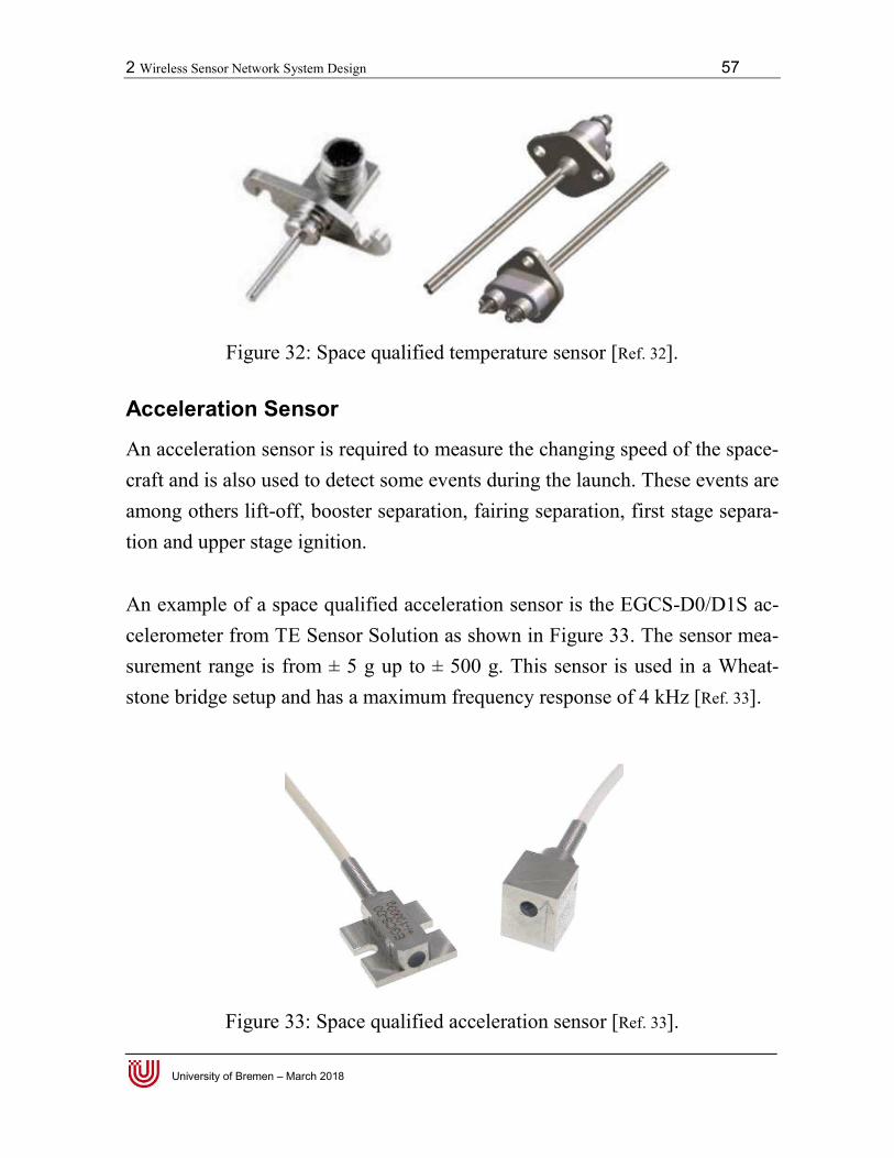
2 Wireless Sensor Network System Design 57
University of Bremen – March 2018
Figure 32: Space qualified temperature sensor [Ref. 32].
Acceleration Sensor
An acceleration sensor is required to measure the changing speed of the space-craft and is also used to detect some events during the launch. These events are among others lift-off, booster separation, fairing separation, first stage separa-tion and upper stage ignition. An example of a space qualified acceleration sensor is the EGCS-D0/D1S ac-celerometer from TE Sensor Solution as shown in Figure 33. The sensor mea-surement range is from ± 5 g up to ± 500 g. This sensor is used in a Wheat-stone bridge setup and has a maximum frequency response of 4 kHz [Ref. 33].
Figure 33: Space qualified acceleration sensor [Ref. 33].
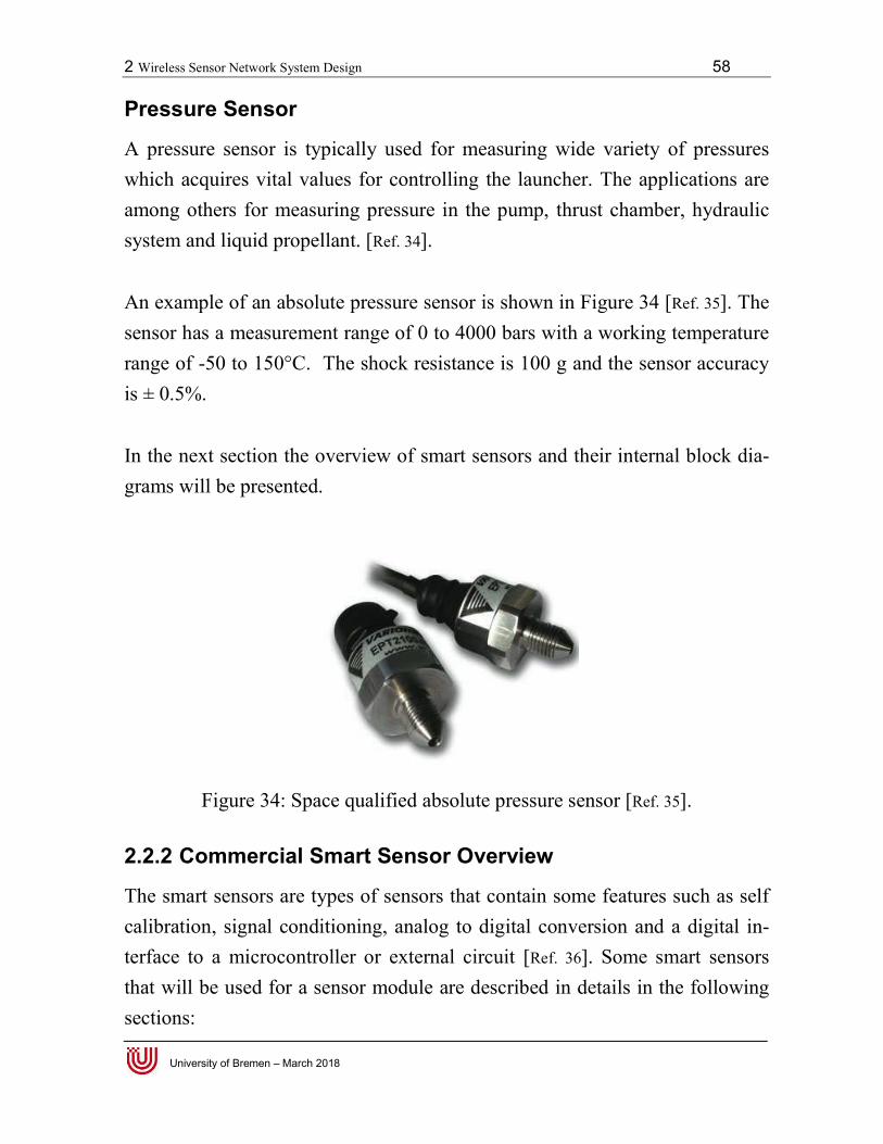
2 Wireless Sensor Network System Design 58
University of Bremen – March 2018
Pressure Sensor
A pressure sensor is typically used for measuring wide variety of pressures which acquires vital values for controlling the launcher. The applications are among others for measuring pressure in the pump, thrust chamber, hydraulic system and liquid propellant. [Ref. 34]. An example of an absolute pressure sensor is shown in Figure 34 [Ref. 35]. The sensor has a measurement range of 0 to 4000 bars with a working temperature range of -50 to 150°C. The shock resistance is 100 g and the sensor accuracy is ± 0.5%. In the next section the overview of smart sensors and their internal block dia-grams will be presented.
Figure 34: Space qualified absolute pressure sensor [Ref. 35].
2.2.2 Commercial Smart Sensor Overview
The smart sensors are types of sensors that contain some features such as self calibration, signal conditioning, analog to digital conversion and a digital in-terface to a microcontroller or external circuit [Ref. 36]. Some smart sensors that will be used for a sensor module are described in details in the following sections:
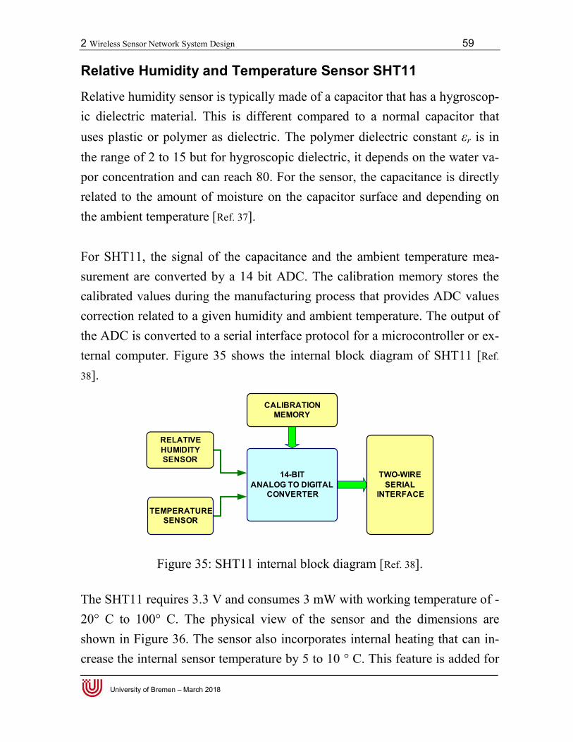
2 Wireless Sensor Network System Design 59
University of Bremen – March 2018
Relative Humidity and Temperature Sensor SHT11
Relative humidity sensor is typically made of a capacitor that has a hygroscop-ic dielectric material. This is different compared to a normal capacitor that uses plastic or polymer as dielectric. The polymer dielectric constant εr is in the range of 2 to 15 but for hygroscopic dielectric, it depends on the water va-por concentration and can reach 80. For the sensor, the capacitance is directly related to the amount of moisture on the capacitor surface and depending on the ambient temperature [Ref. 37]. For SHT11, the signal of the capacitance and the ambient temperature mea-surement are converted by a 14 bit ADC. The calibration memory stores the calibrated values during the manufacturing process that provides ADC values correction related to a given humidity and ambient temperature. The output of the ADC is converted to a serial interface protocol for a microcontroller or ex-ternal computer. Figure 35 shows the internal block diagram of SHT11 [Ref.
38].
RELATIVEHUMIDITYSENSOR
TEMPERATURESENSOR
14-BITANALOG TO DIGITAL
CONVERTER
CALIBRATIONMEMORY
TWO-WIRE SERIAL
INTERFACE
Figure 35: SHT11 internal block diagram [Ref. 38].
The SHT11 requires 3.3 V and consumes 3 mW with working temperature of -20° C to 100° C. The physical view of the sensor and the dimensions are shown in Figure 36. The sensor also incorporates internal heating that can in-crease the internal sensor temperature by 5 to 10 ° C. This feature is added for
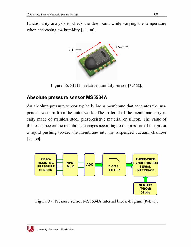
2 Wireless Sensor Network System Design 60
University of Bremen – March 2018
functionality analysis to check the dew point while varying the temperature when decreasing the humidity [Ref. 38].
Figure 36: SHT11 relative humidity sensor [Ref. 38].
Absolute pressure sensor MS5534A
An absolute pressure sensor typically has a membrane that separates the sus-pended vacuum from the outer world. The material of the membrane is typi-cally made of stainless steel, piezoresistive material or silicon. The value of the resistance on the membrane changes according to the pressure of the gas or a liquid pushing toward the membrane into the suspended vacuum chamber [Ref. 39].
DIGITALFILTER
PIEZO-RESISTIVEPRESSURE
SENSOR
INPUTMUX ADC
THREE-WIRESYNCHRONOUS
SERIALINTERFACE
MEMORY(PROM)64 bits
Figure 37: Pressure sensor MS5534A internal block diagram [Ref. 40].
7.47 mm 4.94 mm

2 Wireless Sensor Network System Design 61
University of Bremen – March 2018
The MS5534 absolute pressures sensor has a measurement range of 300 - 1100 mbar. It operates with 3.3 V and consumes 3.3 mW in measurement mode. There are several piezoresistors used for the measurements and these are con-nected to a multiplexer circuit in front of ADC input. Digital filtering is ap-plied to filter the ADC values before sending them to a serial interface circuit that communicates with a microcontroller or external processor. A programm-able read only memory (PROM) is required to store calibrated values during the manufacturing process. Figure 37 shows the internal block diagram of the MS5534A [Ref. 40].
Figure 38: MS5534A pressure sensor dimension [Ref. 40].
Three Axis Acceleration Sensor ADXL345
A Microelectromechanical systems (MEMS) acceleration sensor is used wide-ly and its application keeps growing in recent years [Ref. 41]. The MEMS acce-leration sensor is essential for automotive and consumer application such as handheld equipments because of its miniaturized size and its high precision. The sensor typically consists of capacitor array combs with mass connected to positive electrodes and placed in the middle. The negative electrodes are usually bounded to the body. The change of velocity alters the position of the combs. The change between the combs’ distance results in capacitor values as shows in Figure 40 a) [Ref. 42].
9.15 mm
9.15 mm
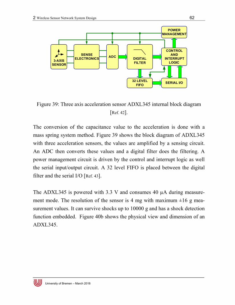
2 Wireless Sensor Network System Design 62
University of Bremen – March 2018
DIGITALFILTER3-AXIS
SENSOR
SENSEELECTRONICS ADC
CONTROL AND
INTERRUPT LOGIC
SERIAL I/O32 LEVELFIFO
POWERMANAGEMENT
Figure 39: Three axis acceleration sensor ADXL345 internal block diagram [Ref. 42].
The conversion of the capacitance value to the acceleration is done with a mass spring system method. Figure 39 shows the block diagram of ADXL345 with three acceleration sensors, the values are amplified by a sensing circuit. An ADC then converts these values and a digital filter does the filtering. A power management circuit is driven by the control and interrupt logic as well the serial input/output circuit. A 32 level FIFO is placed between the digital filter and the serial I/O [Ref. 43]. The ADXL345 is powered with 3.3 V and consumes 40 µA during measure-ment mode. The resolution of the sensor is 4 mg with maximum ±16 g mea-surement values. It can survive shocks up to 10000 g and has a shock detection function embedded. Figure 40b shows the physical view and dimension of an ADXL345.
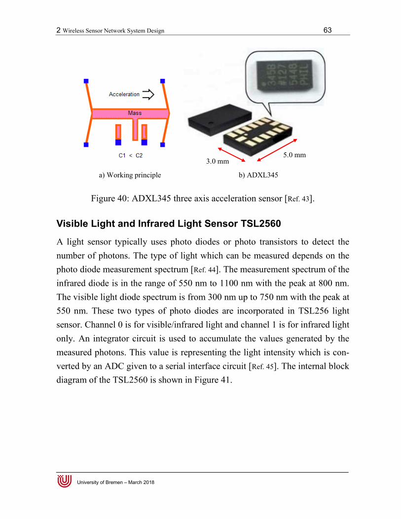
2 Wireless Sensor Network System Design 63
University of Bremen – March 2018
a) Working principle b) ADXL345
Figure 40: ADXL345 three axis acceleration sensor [Ref. 43].
Visible Light and Infrared Light Sensor TSL2560
A light sensor typically uses photo diodes or photo transistors to detect the number of photons. The type of light which can be measured depends on the photo diode measurement spectrum [Ref. 44]. The measurement spectrum of the infrared diode is in the range of 550 nm to 1100 nm with the peak at 800 nm. The visible light diode spectrum is from 300 nm up to 750 nm with the peak at 550 nm. These two types of photo diodes are incorporated in TSL256 light sensor. Channel 0 is for visible/infrared light and channel 1 is for infrared light only. An integrator circuit is used to accumulate the values generated by the measured photons. This value is representing the light intensity which is con-verted by an ADC given to a serial interface circuit [Ref. 45]. The internal block diagram of the TSL2560 is shown in Figure 41.
3.0 mm 5.0 mm
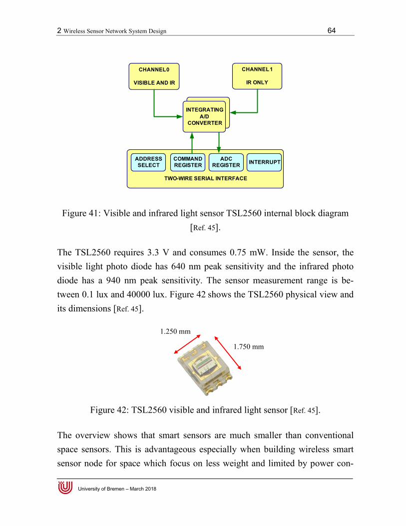
2 Wireless Sensor Network System Design 64
University of Bremen – March 2018
CHANNEL 0
VISIBLE AND IR
CHANNEL 1
IR ONLY
INTEGRATINGA/D
CONVERTER
TWO-WIRE SERIAL INTERFACE
ADDRESSSELECT
COMMANDREGISTER
ADCREGISTER INTERRUPT
Figure 41: Visible and infrared light sensor TSL2560 internal block diagram [Ref. 45].
The TSL2560 requires 3.3 V and consumes 0.75 mW. Inside the sensor, the visible light photo diode has 640 nm peak sensitivity and the infrared photo diode has a 940 nm peak sensitivity. The sensor measurement range is be-tween 0.1 lux and 40000 lux. Figure 42 shows the TSL2560 physical view and its dimensions [Ref. 45].
Figure 42: TSL2560 visible and infrared light sensor [Ref. 45].
The overview shows that smart sensors are much smaller than conventional space sensors. This is advantageous especially when building wireless smart sensor node for space which focus on less weight and limited by power con-
1.750 mm
1.250 mm
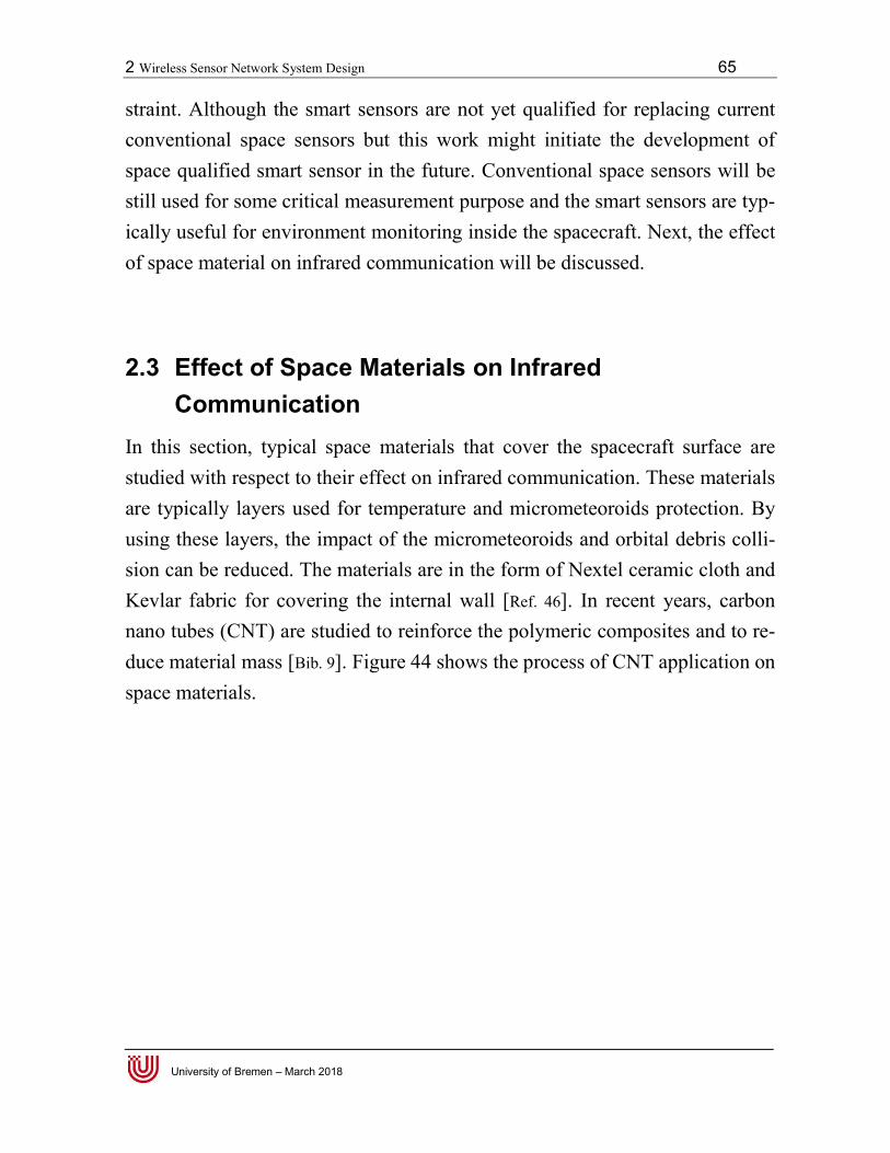
2 Wireless Sensor Network System Design 65
University of Bremen – March 2018
straint. Although the smart sensors are not yet qualified for replacing current conventional space sensors but this work might initiate the development of space qualified smart sensor in the future. Conventional space sensors will be still used for some critical measurement purpose and the smart sensors are typ-ically useful for environment monitoring inside the spacecraft. Next, the effect of space material on infrared communication will be discussed.
2.3 Effect of Space Materials on Infrared Communication
In this section, typical space materials that cover the spacecraft surface are studied with respect to their effect on infrared communication. These materials are typically layers used for temperature and micrometeoroids protection. By using these layers, the impact of the micrometeoroids and orbital debris colli-sion can be reduced. The materials are in the form of Nextel ceramic cloth and Kevlar fabric for covering the internal wall [Ref. 46]. In recent years, carbon nano tubes (CNT) are studied to reinforce the polymeric composites and to re-duce material mass [Bib. 9]. Figure 44 shows the process of CNT application on space materials.
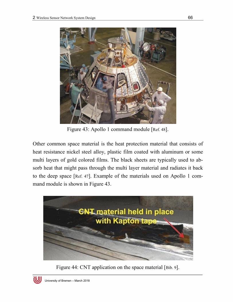
2 Wireless Sensor Network System Design
University of Bremen – March 2018
Figure 43: Apollo
Other common space material is the heat protection material that consists of heat resistance nickel steel alloy, plastic film coated with multi layers of gold coloredsorb heat that might pass through the multi layer material and radiates it back to the deep space [Ref. 47]. Example of the materials used on mand module is shown in Figure
Figure 44: CNT application on the space material [
Sensor Network System Design
Apollo 1 command module [Ref. 48].
Other common space material is the heat protection material that consists of ickel steel alloy, plastic film coated with aluminum
colored films. The black sheets are typically used to asorb heat that might pass through the multi layer material and radiates it back
]. Example of the materials used on ApolloFigure 43.
: CNT application on the space material [Bib.
66
Other common space material is the heat protection material that consists of aluminum or some
films. The black sheets are typically used to ab-sorb heat that might pass through the multi layer material and radiates it back
Apollo 1 com-
Bib. 9].
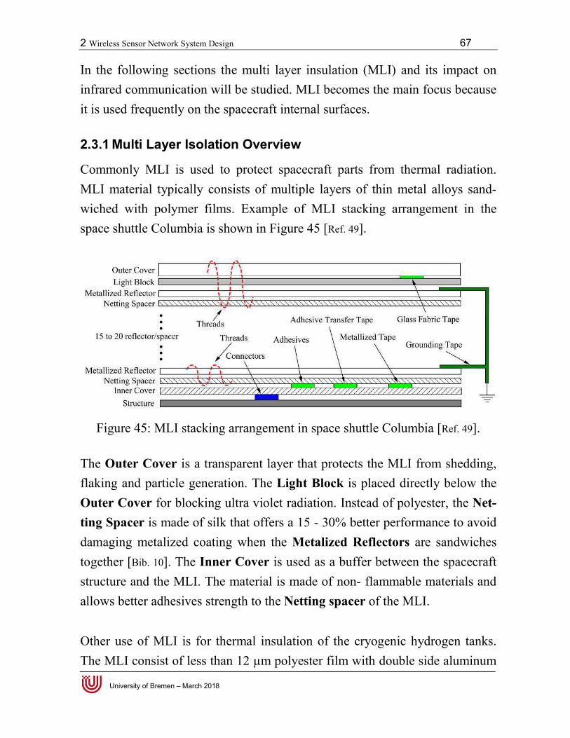
2 Wireless Sensor Network System Design 67
University of Bremen – March 2018
In the following sections the multi layer insulation (MLI) and its impact on infrared communication will be studied. MLI becomes the main focus because it is used frequently on the spacecraft internal surfaces.
2.3.1 Multi Layer Isolation Overview
Commonly MLI is used to protect spacecraft parts from thermal radiation. MLI material typically consists of multiple layers of thin metal alloys sand-wiched with polymer films. Example of MLI stacking arrangement in the space shuttle Columbia is shown in Figure 45 [Ref. 49].
Figure 45: MLI stacking arrangement in space shuttle Columbia [Ref. 49].
The Outer Cover is a transparent layer that protects the MLI from shedding, flaking and particle generation. The Light Block is placed directly below the Outer Cover for blocking ultra violet radiation. Instead of polyester, the Net-ting Spacer is made of silk that offers a 15 - 30% better performance to avoid damaging metalized coating when the Metalized Reflectors are sandwiches together [Bib. 10]. The Inner Cover is used as a buffer between the spacecraft structure and the MLI. The material is made of non- flammable materials and allows better adhesives strength to the Netting spacer of the MLI. Other use of MLI is for thermal insulation of the cryogenic hydrogen tanks. The MLI consist of less than 12 µm polyester film with double side aluminum
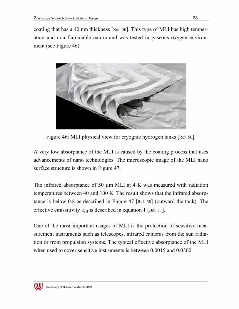
2 Wireless Sensor Network System Design 68
University of Bremen – March 2018
coating that has a 40 nm thickness [Ref. 50]. This type of MLI has high temper-ature and non flammable nature and was tested in gaseous oxygen environ-ment (see Figure 46).
Figure 46: MLI physical view for cryognic hydrogen tanks [Ref. 50].
A very low absorptance of the MLI is caused by the coating process that uses advancements of nano technologies. The microscopic image of the MLI nano surface structure is shown in Figure 47. The infrared absorptance of 50 µm MLI at 4 K was measured with radiation temperatures between 40 and 100 K. The result shows that the infrared absorp-tance is below 0.8 as described in Figure 47 [Ref. 50] (outward the tank). The effective emissitivity εeff is described in equation 1 [Bib. 11].
One of the most important usages of MLI is the protection of sensitive mea-surement instruments such as telescopes, infrared cameras from the sun radia-tion or from propulsion systems. The typical effective absorptance of the MLI when used to cover sensitive instruments is between 0.0015 and 0.0300.
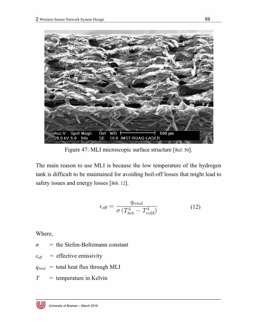
2 Wireless Sensor Network System Design 69
University of Bremen – March 2018
Figure 47: MLI microscopic surface structure [Ref. 50].
The main reason to use MLI is because the low temperature of the hydrogen tank is difficult to be maintained for avoiding boil-off losses that might lead to safety issues and energy losses [Bib. 12].
Where,
σ = the Stefen-Boltzmann constant
εeff = effective emissivity
qtotal = total heat flux through MLI
T = temperature in Kelvin
(12)
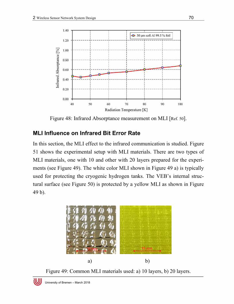
2 Wireless Sensor Network System Design
University of Bremen – March 2018
Figure 48: Infrared Absor
MLI Influence on Infrared Bit Error Rate
In this section, the MLI effect to the infrared communication is studied. 51 shows the experimental setup with MLI materials. There are two types of MLI materials, one with 10 and ments (see Figure 49). The white color MLI shown in used for protecting the cryogenic hydrogen tanks. The VEB’s internal strutural surface (see Figure 5049 b).
a)
Figure 49: Common MLI materials used: a) 10 layers, b) 20 layers.
Sensor Network System Design
: Infrared Absorptance measurement on MLI [Ref.
MLI Influence on Infrared Bit Error Rate
In this section, the MLI effect to the infrared communication is studied. shows the experimental setup with MLI materials. There are two types of
with 10 and other with 20 layers prepared for the experThe white color MLI shown in Figure 49 a) is typicryogenic hydrogen tanks. The VEB’s internal stru50) is protected by a yellow MLI as shown in
a) b)
MLI materials used: a) 10 layers, b) 20 layers.
70
Ref. 50].
In this section, the MLI effect to the infrared communication is studied. Figure shows the experimental setup with MLI materials. There are two types of
for the experi-a) is typically
cryogenic hydrogen tanks. The VEB’s internal struc-) is protected by a yellow MLI as shown in Figure
MLI materials used: a) 10 layers, b) 20 layers.
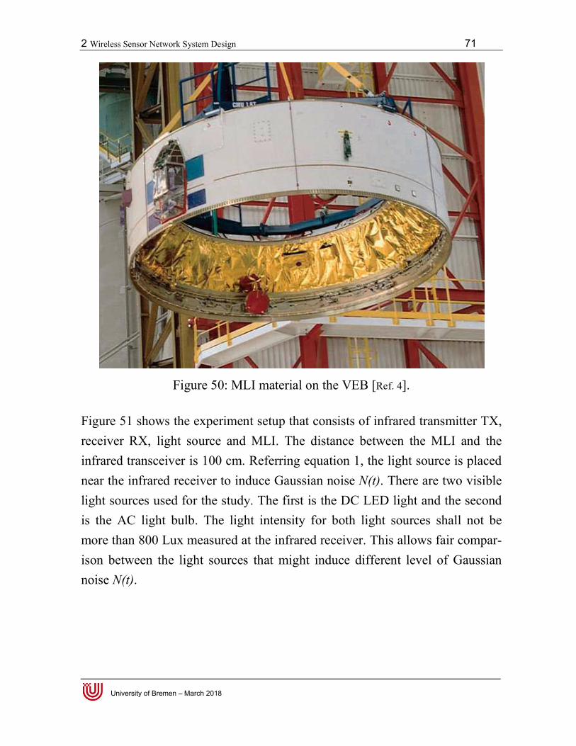
2 Wireless Sensor Network System Design 71
University of Bremen – March 2018
Figure 50: MLI material on the VEB [Ref. 4].
Figure 51 shows the experiment setup that consists of infrared transmitter TX, receiver RX, light source and MLI. The distance between the MLI and the infrared transceiver is 100 cm. Referring equation 1, the light source is placed near the infrared receiver to induce Gaussian noise N(t). There are two visible light sources used for the study. The first is the DC LED light and the second is the AC light bulb. The light intensity for both light sources shall not be more than 800 Lux measured at the infrared receiver. This allows fair compar-ison between the light sources that might induce different level of Gaussian noise N(t).
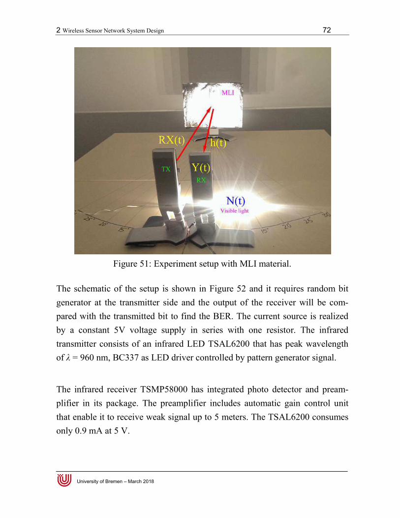
2 Wireless Sensor Network System Design 72
University of Bremen – March 2018
Figure 51: Experiment setup with MLI material.
The schematic of the setup is shown in Figure 52 and it requires random bit generator at the transmitter side and the output of the receiver will be com-pared with the transmitted bit to find the BER. The current source is realized by a constant 5V voltage supply in series with one resistor. The infrared transmitter consists of an infrared LED TSAL6200 that has peak wavelength of λ = 960 nm, BC337 as LED driver controlled by pattern generator signal.
The infrared receiver TSMP58000 has integrated photo detector and pream-plifier in its package. The preamplifier includes automatic gain control unit that enable it to receive weak signal up to 5 meters. The TSAL6200 consumes only 0.9 mA at 5 V.
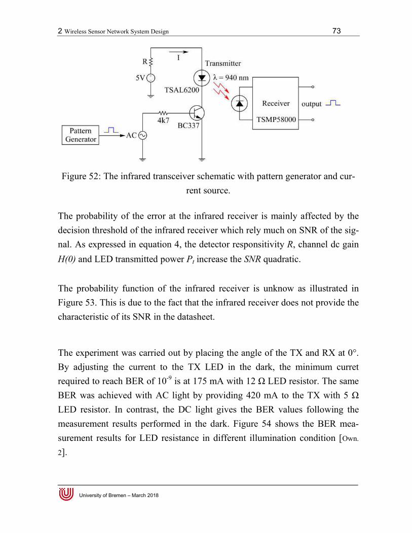
2 Wireless Sensor Network System Design
University of Bremen – March 2018
Figure 52: The infrared transceiver schematic with pattern
The probability of the error at the infrared receiver is mainly affected by the decision threshold of the infrared receivernal. As expressed in equation 4, the detector responsitivity H(0) and LED transmitted power The probability function of the infrared receiver is unknow as illustrated in Figure 53. This is due to the fact that the infrared receivecharacteristic of its SNR in the datasheet.
The experiment was carried out by placing the angle of the TX and RX By adjusting the current to the TX LED in the dark, the minimum curret required to reach BER of 10BER was achieved with AC light by providing 420 mA to the TX with 5 LED resistor. In contrast, the DC light givmeasurement results performed in the dark.surement results for LED resistance in different illumination condition [2].
Sensor Network System Design
: The infrared transceiver schematic with pattern generator and curent source.
The probability of the error at the infrared receiver is mainly affected by the of the infrared receiver which rely much on SNR of the si
nal. As expressed in equation 4, the detector responsitivity R, chanand LED transmitted power Pt increase the SNR quadratic.
The probability function of the infrared receiver is unknow as illustrated in . This is due to the fact that the infrared receiver does not provide the
characteristic of its SNR in the datasheet.
The experiment was carried out by placing the angle of the TX and RX By adjusting the current to the TX LED in the dark, the minimum curret required to reach BER of 10-9 is at 175 mA with 12 Ω LED resistor. The BER was achieved with AC light by providing 420 mA to the TX with 5
. In contrast, the DC light gives the BER values following the measurement results performed in the dark. Figure 54 shows the BER mesurement results for LED resistance in different illumination condition [
73
generator and cur-
The probability of the error at the infrared receiver is mainly affected by the SNR of the sig-
, channel dc gain
The probability function of the infrared receiver is unknow as illustrated in r does not provide the
The experiment was carried out by placing the angle of the TX and RX at 0°. By adjusting the current to the TX LED in the dark, the minimum curret
resistor. The same BER was achieved with AC light by providing 420 mA to the TX with 5 Ω
es the BER values following the shows the BER mea-
surement results for LED resistance in different illumination condition [Own.

2 Wireless Sensor Network System Design 74
University of Bremen – March 2018
Figure 53: Unknown probability function of the experiment.
One reason that might cause the AC light delivers such high noise to the infra-red channel because its light spectrum contains high infrared components.
Figure 54: Bit-error-rate (BER) measurement versus LED current in different illumination conditions [Own. 2]
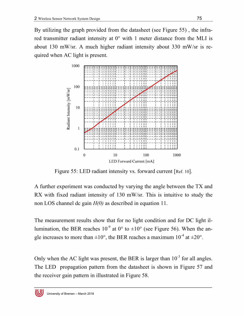
2 Wireless Sensor Network System Design 75
University of Bremen – March 2018
By utilizing the graph provided from the datasheet (see Figure 55) , the infra-red transmitter radiant intensity at 0° with 1 meter distance from the MLI is about 130 mW/sr. A much higher radiant intensity about 330 mW/sr is re-quired when AC light is present.
Figure 55: LED radiant intensity vs. forward current [Ref. 10].
A further experiment was conducted by varying the angle between the TX and RX with fixed radiant intensity of 130 mW/sr. This is intuitive to study the non LOS channel dc gain H(0) as described in equation 11. The measurement results show that for no light condition and for DC light il-lumination, the BER reaches 10-9 at 0° to ±10° (see Figure 56). When the an-gle increases to more than ±10°, the BER reaches a maximum 10-4 at ±20°.
Only when the AC light was present, the BER is larger than 10-3 for all angles. The LED propagation pattern from the datasheet is shown in Figure 57 and the receiver gain pattern in illustrated in Figure 58.
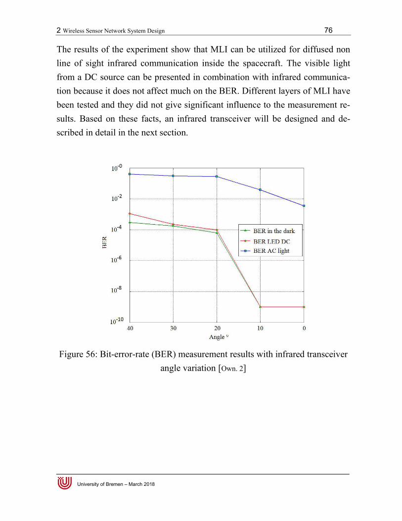
2 Wireless Sensor Network System Design 76
University of Bremen – March 2018
The results of the experiment show that MLI can be utilized for diffused non line of sight infrared communication inside the spacecraft. The visible light from a DC source can be presented in combination with infrared communica-tion because it does not affect much on the BER. Different layers of MLI have been tested and they did not give significant influence to the measurement re-sults. Based on these facts, an infrared transceiver will be designed and de-scribed in detail in the next section.
Figure 56: Bit-error-rate (BER) measurement results with infrared transceiver angle variation [Own. 2]
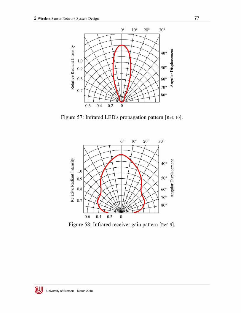
2 Wireless Sensor Network System Design 77
University of Bremen – March 2018
Figure 57: Infrared LED's propagation pattern [Ref. 10].
Figure 58: Infrared receiver gain pattern [Ref. 9].
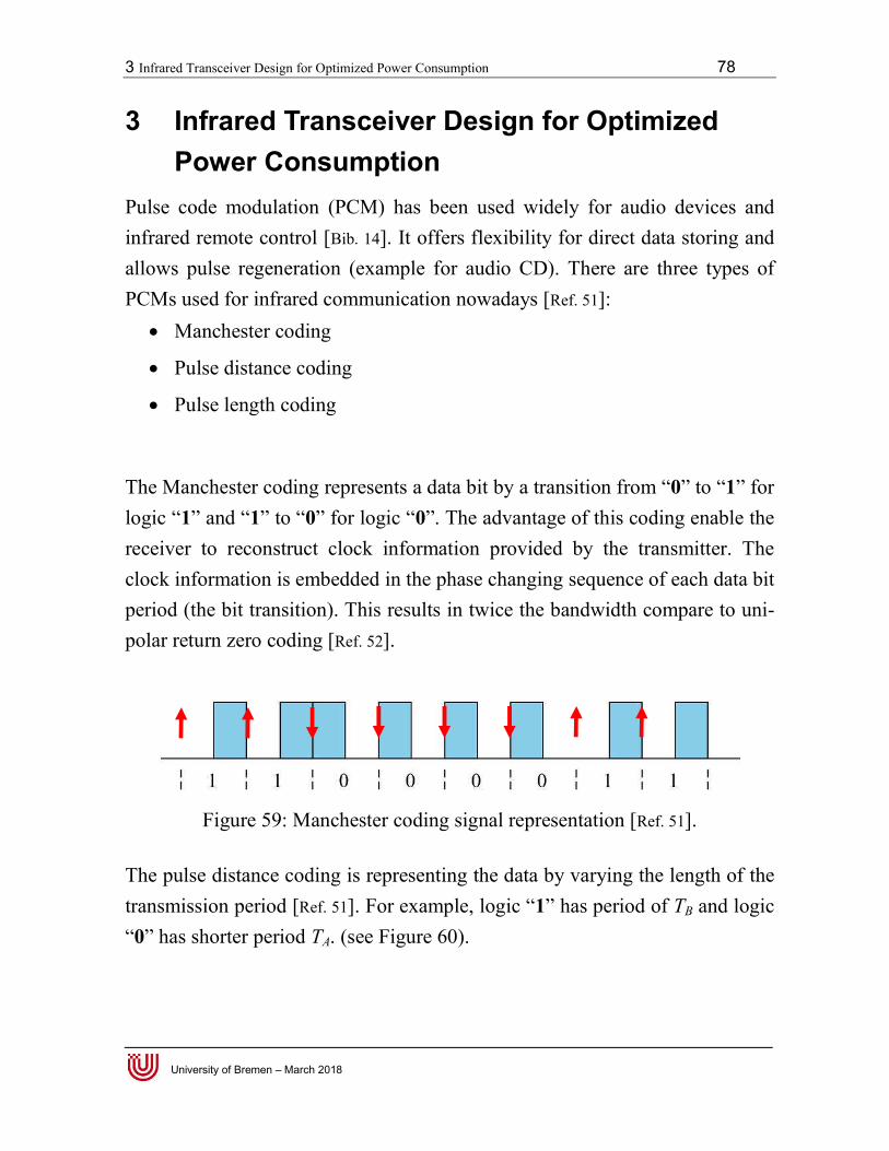
3 Infrared Transceiver Design for Optimized Power Consumption 78
University of Bremen – March 2018
3 Infrared Transceiver Design for Optimized Power Consumption
Pulse code modulation (PCM) has been used widely for audio devices and infrared remote control [Bib. 14]. It offers flexibility for direct data storing and allows pulse regeneration (example for audio CD). There are three types of PCMs used for infrared communication nowadays [Ref. 51]: Manchester coding
Pulse distance coding
Pulse length coding
The Manchester coding represents a data bit by a transition from “0” to “1” for logic “1” and “1” to “0” for logic “0”. The advantage of this coding enable the receiver to reconstruct clock information provided by the transmitter. The clock information is embedded in the phase changing sequence of each data bit period (the bit transition). This results in twice the bandwidth compare to uni-polar return zero coding [Ref. 52].
Figure 59: Manchester coding signal representation [Ref. 51].
The pulse distance coding is representing the data by varying the length of the transmission period [Ref. 51]. For example, logic “1” has period of TB and logic “0” has shorter period TA. (see Figure 60).
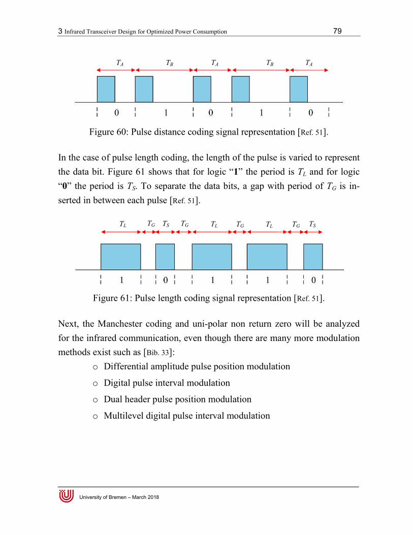
3 Infrared Transceiver Design for Optimized Power Consumption 79
University of Bremen – March 2018
Figure 60: Pulse distance coding signal representation [Ref. 51].
In the case of pulse length coding, the length of the pulse is varied to represent the data bit. Figure 61 shows that for logic “1” the period is TL and for logic “0” the period is TS. To separate the data bits, a gap with period of TG is in-serted in between each pulse [Ref. 51].
Figure 61: Pulse length coding signal representation [Ref. 51].
Next, the Manchester coding and uni-polar non return zero will be analyzed for the infrared communication, even though there are many more modulation methods exist such as [Bib. 33]:
o Differential amplitude pulse position modulation
o Digital pulse interval modulation
o Dual header pulse position modulation
o Multilevel digital pulse interval modulation
TA TB TB TA TA
TL TS TG TG TS TL TG TL TG

3 Infrared Transceiver Design for Optimized Power Consumption 80
University of Bremen – March 2018
3.1 Modulation Selection of the Infrared Physical Layer
The power spectral density of Manchester coding and uni-polar non return ze-ro coding are analyzed for better understanding of the design. Although the uni-polar non return zero power spectrum density (see equation 13, [Bib. 15]) shows that it requires more power as the signals move toward DC but it offers simpler hardware design.
Where A is the amplitude of the signal, Tb is the period of the signal represented by bandwidth Rb = 1/Tb. The more advance coding it the well known Manchester coding. This coding offer clock recovery and does not con-tain DC components (see equation 14, [Bib. 15]). This becomes challenging when designing the hardware because the incoming Manchester signal needs edge detection function for synchronizing the internal Manchester clock before the zeros and pulses can be generated. Although the Manchester clock at the receiver part is possible to be generated from the incoming signal edges, but that causes hardware overhead.
Figure 62 shows the spectral density comparison between Manchester coding and uni-polar non return zero coding. The Manchester coding PSD amplitude is normalized for better graph comparison.
(13)
(14)
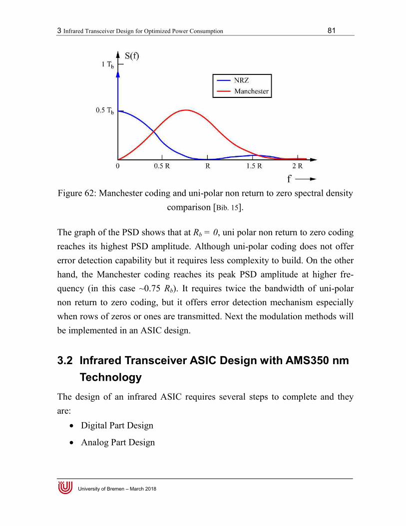
3 Infrared Transceiver Design for Optimized Power Consumption 81
University of Bremen – March 2018
Figure 62: Manchester coding and uni-polar non return to zero spectral density comparison [Bib. 15].
The graph of the PSD shows that at Rb = 0, uni polar non return to zero coding reaches its highest PSD amplitude. Although uni-polar coding does not offer error detection capability but it requires less complexity to build. On the other hand, the Manchester coding reaches its peak PSD amplitude at higher fre-quency (in this case ~0.75 Rb). It requires twice the bandwidth of uni-polar non return to zero coding, but it offers error detection mechanism especially when rows of zeros or ones are transmitted. Next the modulation methods will be implemented in an ASIC design.
3.2 Infrared Transceiver ASIC Design with AMS350 nm Technology
The design of an infrared ASIC requires several steps to complete and they are:
Digital Part Design
Analog Part Design
3 Infrared Transceiver Design for Optimized Power Consumption 82
University of Bremen – March 2018
Substituting Clock Synchronous Digital Part with Event Driven Analog
Part to save energy
The analog mixed signal 350 nm technologies are used to realize the infrared transceiver ASICs design. The technology is provided by an Austrian multina-tional semiconductor manufacturer, Austria Mikro Systeme AG (referred to as AMS) [Ref. 53].
The design of the ASICs is carried out to optimize power consumption. This is achieved by simplifying the hardware building blocks and by replacing the critical synchronous module with asynchronous circuit. Since the clock always present in synchronized circuit, the high current consumption during clock transition is happening all the time. This current consumption is minimized by either using asynchronous circuit or analog circuit with capacitor to store state when state machine is required [Bib. 59]. In this work, the asynchronous digital circuit is replaced by analog astabile multivibrator is to overcome the draw-back that might related to global clock issues (e.g. cross talk, critical path, etc.) [Bib. 60]. This implicates less energy consumptions by having the analog cir-cuit with simple design. This leads to less transistors compared with synthe-sized digital circuit [Bib. 61, Bib. 62]. Next section will show how a simple ana-log circuit is used to replace digital pulse detection and pulse recovery circuit.
A 9600 bandwidth is selected for realizing the infrared transceiver. The simu-lation for this bandwidth was performed in Matlab with P. Welch algorithm which estimates and compares the spectral density in of both modulation types [Bib. 47]. In the simulation, a random bit stream was generated for both cod-ings. The simulation results in Figure 63 show that at 9600 baud the uni-polar coding consumes less power than the Manchester coding by approximately -20dB. At 2400 baud, the Manchester coding reduces the power consumption by -6 dB. This result shows that minimum power consumption is achieved at 9600 baud with almost -65 dB for uni-polar coding.

3 Infrared Transceiver Design for Optimized Power Consumption 83
University of Bremen – March 2018
Such communication speed is sufficient especially for compacted data from smart sensors, such those temperature, air pressure, air humidity and accelera-tion sensors.
Figure 63: Manchester and uni-polar return to zero spectral density simulation [Own. 3].
3.2.1 Manchester coding ASIC development
The design of the hardware is initialized by grouping the hardware blocks ac-cording to their functionality. The block diagram of the Manchester coding transmitter is divided into sub blocks and they are described as following, UART to Manchester block contains the following sub blocks:
Manchester clock Generator block: This block generates Man-
chester clock with 19200 Hz or twice of the transmission baud (see
signal M_clk).
Manchester block: This block uses a logical operator XOR to
generate a Manchester output signal by inverting the UART_in
3 Infrared Transceiver Design for Optimized Power Consumption 84
University of Bremen – March 2018
signal and XORing it with the Manchester clock output. (see sig-
nal Manchester_out = UART_in XOR M_clk).
IrDA 3/16 pulse shaping block: The input signal Manchester_out is
shaped by reducing the pulse width to 3/16 of the baud period. In this
case the 9600 baud has period of 104 µs and was reduced to 20 µs (see
signal 3/16_out). The pulse shaping block is required to meet IrDa
physical layer standard in order to reduce power consumption of the in-
frared LED by 85 % [Ref. 26].
and the Manchester receiver blocks are: IrDA 3/16 pulse recovery block: The input signal from the infrared re-
ceiver IR_receiver is inverted (see signal 3/16_in) and its pulse period
is extended to 52 µs (because the Manchester code uses twice of the
bandwidth, see signal Manchester_in).
Manchester to UART block contains the following sub blocks:
Manchester edge detector block: This block detects the ris-
ing/falling edges of the 3/16_in signal from IrDA 3/16 pulse re-
covery block. When the rising edge from the start bit is detected,
the block will generate 21 short pulses (see signal edge_detector)
triggered by the input signal. The state machine in the edge detec-
tor compares the previous input state with the current input state
for detecting if any Manchester pulse transitions exist. A timer is
set to measure the length of each detected edge. If the timer is
valid and there is no edge detected at the input, the error flag is set
and the received bits are erased.
Manchester clock recovery block: The signal received from the
Manchester edge detector block is used to recover the Manches-
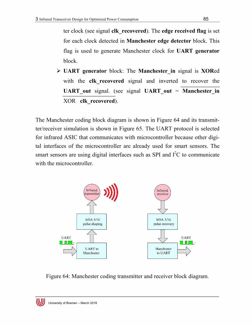
3 Infrared Transceiver Design for Optimized Power Consumption 85
University of Bremen – March 2018
ter clock (see signal clk_recovered). The edge received flag is set
for each clock detected in Manchester edge detector block. This
flag is used to generate Manchester clock for UART generator
block.
UART generator block: The Manchester_in signal is XORed
with the clk_recovered signal and inverted to recover the
UART_out signal. (see signal UART_out = Manchester_in
XOR clk_recovered).
The Manchester coding block diagram is shown in Figure 64 and its transmit-ter/receiver simulation is shown in Figure 65. The UART protocol is selected for infrared ASIC that communicates with microcontroller because other digi-tal interfaces of the microcontroller are already used for smart sensors. The smart sensors are using digital interfaces such as SPI and I2C to communicate with the microcontroller.
Figure 64: Manchester coding transmitter and receiver block diagram.
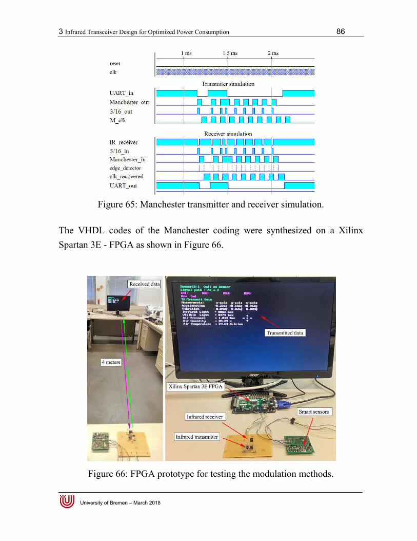
3 Infrared Transceiver Design for Optimized Power Consumption 86
University of Bremen – March 2018
Figure 65: Manchester transmitter and receiver simulation.
The VHDL codes of the Manchester coding were synthesized on a Xilinx Spartan 3E - FPGA as shown in Figure 66.
Figure 66: FPGA prototype for testing the modulation methods.
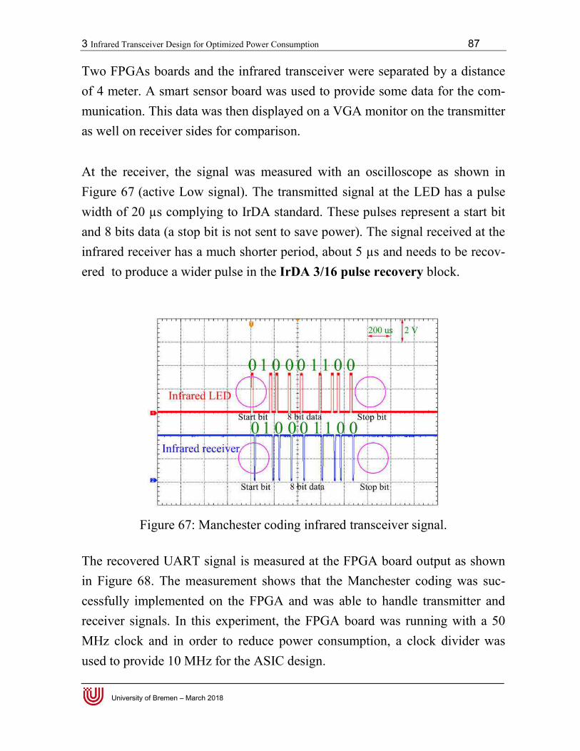
3 Infrared Transceiver Design for Optimized Power Consumption 87
University of Bremen – March 2018
Two FPGAs boards and the infrared transceiver were separated by a distance of 4 meter. A smart sensor board was used to provide some data for the com-munication. This data was then displayed on a VGA monitor on the transmitter as well on receiver sides for comparison. At the receiver, the signal was measured with an oscilloscope as shown in Figure 67 (active Low signal). The transmitted signal at the LED has a pulse width of 20 µs complying to IrDA standard. These pulses represent a start bit and 8 bits data (a stop bit is not sent to save power). The signal received at the infrared receiver has a much shorter period, about 5 µs and needs to be recov-ered to produce a wider pulse in the IrDA 3/16 pulse recovery block.
Figure 67: Manchester coding infrared transceiver signal.
The recovered UART signal is measured at the FPGA board output as shown in Figure 68. The measurement shows that the Manchester coding was suc-cessfully implemented on the FPGA and was able to handle transmitter and receiver signals. In this experiment, the FPGA board was running with a 50 MHz clock and in order to reduce power consumption, a clock divider was used to provide 10 MHz for the ASIC design.
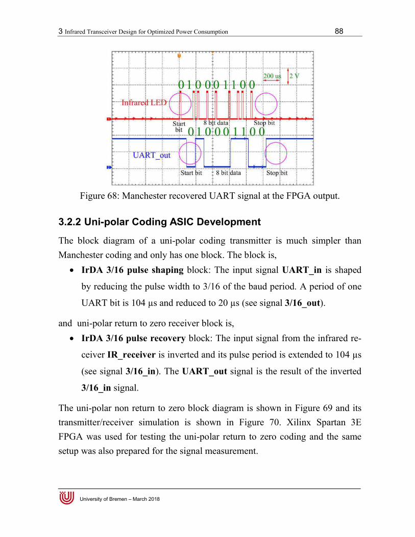
3 Infrared Transceiver Design for Optimized Power Consumption 88
University of Bremen – March 2018
Figure 68: Manchester recovered UART signal at the FPGA output.
3.2.2 Uni-polar Coding ASIC Development
The block diagram of a uni-polar coding transmitter is much simpler than Manchester coding and only has one block. The block is, IrDA 3/16 pulse shaping block: The input signal UART_in is shaped
by reducing the pulse width to 3/16 of the baud period. A period of one
UART bit is 104 µs and reduced to 20 µs (see signal 3/16_out).
and uni-polar return to zero receiver block is, IrDA 3/16 pulse recovery block: The input signal from the infrared re-
ceiver IR_receiver is inverted and its pulse period is extended to 104 µs
(see signal 3/16_in). The UART_out signal is the result of the inverted
3/16_in signal.
The uni-polar non return to zero block diagram is shown in Figure 69 and its transmitter/receiver simulation is shown in Figure 70. Xilinx Spartan 3E FPGA was used for testing the uni-polar return to zero coding and the same setup was also prepared for the signal measurement.
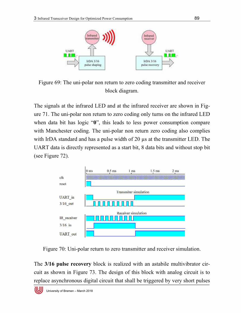
3 Infrared Transceiver Design for Optimized Power Consumption 89
University of Bremen – March 2018
Figure 69: The uni-polar non return to zero coding transmitter and receiver block diagram.
The signals at the infrared LED and at the infrared receiver are shown in Fig-ure 71. The uni-polar non return to zero coding only turns on the infrared LED when data bit has logic “0”, this leads to less power consumption compare with Manchester coding. The uni-polar non return zero coding also complies with IrDA standard and has a pulse width of 20 µs at the transmitter LED. The UART data is directly represented as a start bit, 8 data bits and without stop bit (see Figure 72).
Figure 70: Uni-polar return to zero transmitter and receiver simulation.
The 3/16 pulse recovery block is realized with an astabile multivibrator cir-cuit as shown in Figure 73. The design of this block with analog circuit is to replace asynchronous digital circuit that shall be triggered by very short pulses
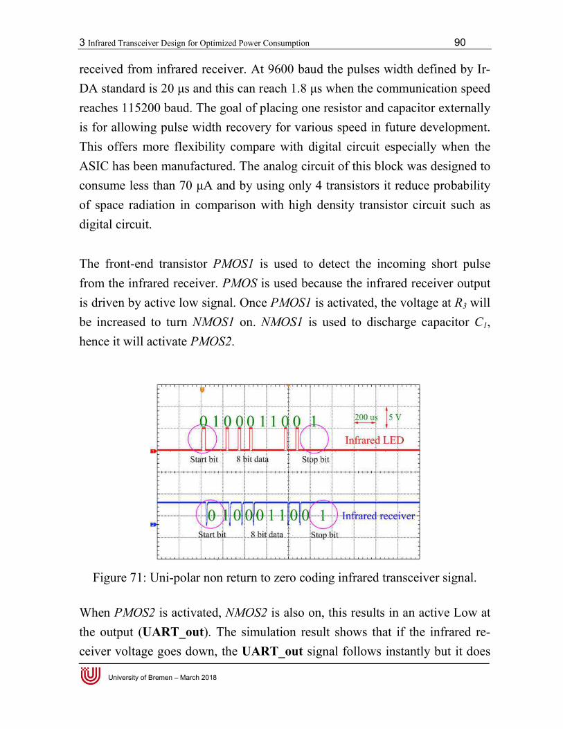
3 Infrared Transceiver Design for Optimized Power Consumption 90
University of Bremen – March 2018
received from infrared receiver. At 9600 baud the pulses width defined by Ir-DA standard is 20 μs and this can reach 1.8 μs when the communication speed reaches 115200 baud. The goal of placing one resistor and capacitor externally is for allowing pulse width recovery for various speed in future development. This offers more flexibility compare with digital circuit especially when the ASIC has been manufactured. The analog circuit of this block was designed to consume less than 70 μA and by using only 4 transistors it reduce probability of space radiation in comparison with high density transistor circuit such as digital circuit. The front-end transistor PMOS1 is used to detect the incoming short pulse from the infrared receiver. PMOS is used because the infrared receiver output is driven by active low signal. Once PMOS1 is activated, the voltage at R3 will be increased to turn NMOS1 on. NMOS1 is used to discharge capacitor C1, hence it will activate PMOS2.
Figure 71: Uni-polar non return to zero coding infrared transceiver signal.
When PMOS2 is activated, NMOS2 is also on, this results in an active Low at the output (UART_out). The simulation result shows that if the infrared re-ceiver voltage goes down, the UART_out signal follows instantly but it does
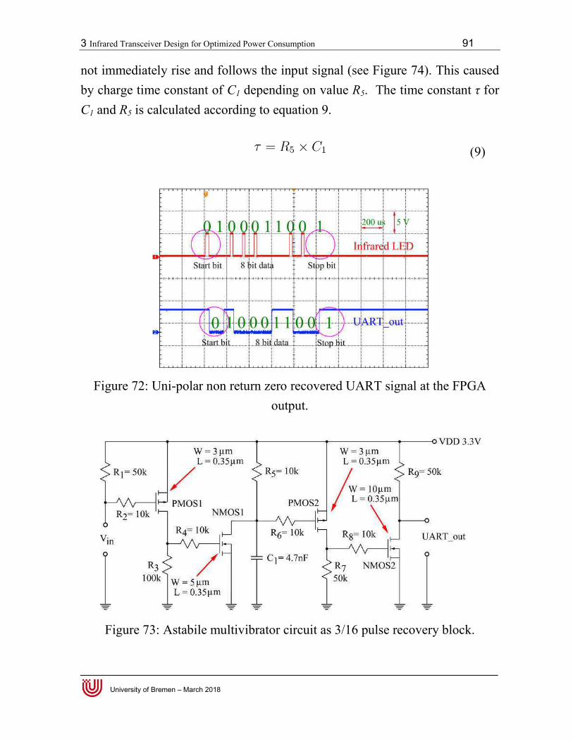
3 Infrared Transceiver Design for Optimized Power Consumption 91
University of Bremen – March 2018
not immediately rise and follows the input signal (see Figure 74). This caused by charge time constant of C1 depending on value R5. The time constant τ for C1 and R5 is calculated according to equation 9.
Figure 72: Uni-polar non return zero recovered UART signal at the FPGA output.
Figure 73: Astabile multivibrator circuit as 3/16 pulse recovery block.
(9)
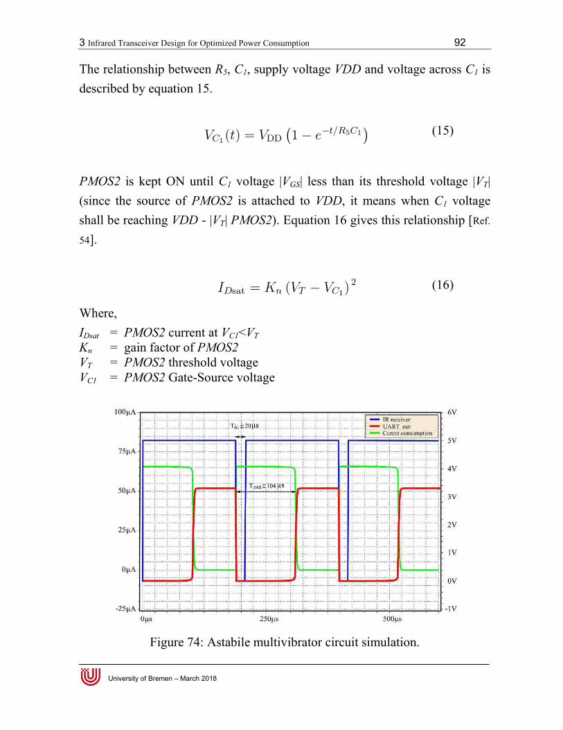
3 Infrared Transceiver Design for Optimized Power Consumption 92
University of Bremen – March 2018
The relationship between R5, C1, supply voltage VDD and voltage across C1 is described by equation 15.
PMOS2 is kept ON until C1 voltage |VGS| less than its threshold voltage |VT| (since the source of PMOS2 is attached to VDD, it means when C1 voltage shall be reaching VDD - |VT| PMOS2). Equation 16 gives this relationship [Ref.
54].
Where, IDsat = PMOS2 current at VC1<VT Kn = gain factor of PMOS2 VT = PMOS2 threshold voltage VC1 = PMOS2 Gate-Source voltage
Figure 74: Astabile multivibrator circuit simulation.
(16)
(15)

3 Infrared Transceiver Design for Optimized Power Consumption 93
University of Bremen – March 2018
The extended pulse width at UART_out is set to 104 µs by adjusting the val-ues of R5 and C1. The current consumption of the circuit was reduced to less than 75 µA through the selection of the transistors width and length (see Fig-ure 73 and Figure 74). The digital circuit has been replaced by this circuit for power optimization.
3.2.3 Infrared transceiver ASIC Design
In this section the layout of the infrared transceiver ASIC based on the mod-ulation methods is carried out. The Cadence Virtuoso Analog Design Envi-ronment [Ref. 56] was used to design the 3/16 pulse recovery circuit while C1 and R5 are placed externally. These two components allow calibration for achieving 104 µs pulse width after the ASIC is manufactured. The digital part was synthesized by Synopsys Design Compiler [Ref. 57] together with Cadence Encounter [Ref. 58]. The Manchester layout has a chip surface of 330 × 330 µm, the uni-polar TX is 130 × 130 µm, the Manchester recovery is 51 × 56 µm and the uni-polar RX is also 51 × 56 µm. The total area required for both of the designs, including 40 input/output pads, is 1800 × 1800 µm (see Figure 75). The power consump-tion estimated for the designs is summarized in Table 7. The Dynamic Power consumption was estimated with 10 ms of simulation using SimVision (from Cadence Design Systems), based on the AMS 350 nm technology parameters. The simulation results were exported as value change dump and were used to estimate the dynamic power consumption using the register transfer logic compiler (RTL).
Table 7: Dynamic power estimation of the digital circuit.
Layout name Instance Leakage Dynamic Total
Power (nW) Power (mW) Power (mW)
Manchester layout 628 0.598 39.89 39.89
Uni-Polar layout 261 0.248 1.47 1.47
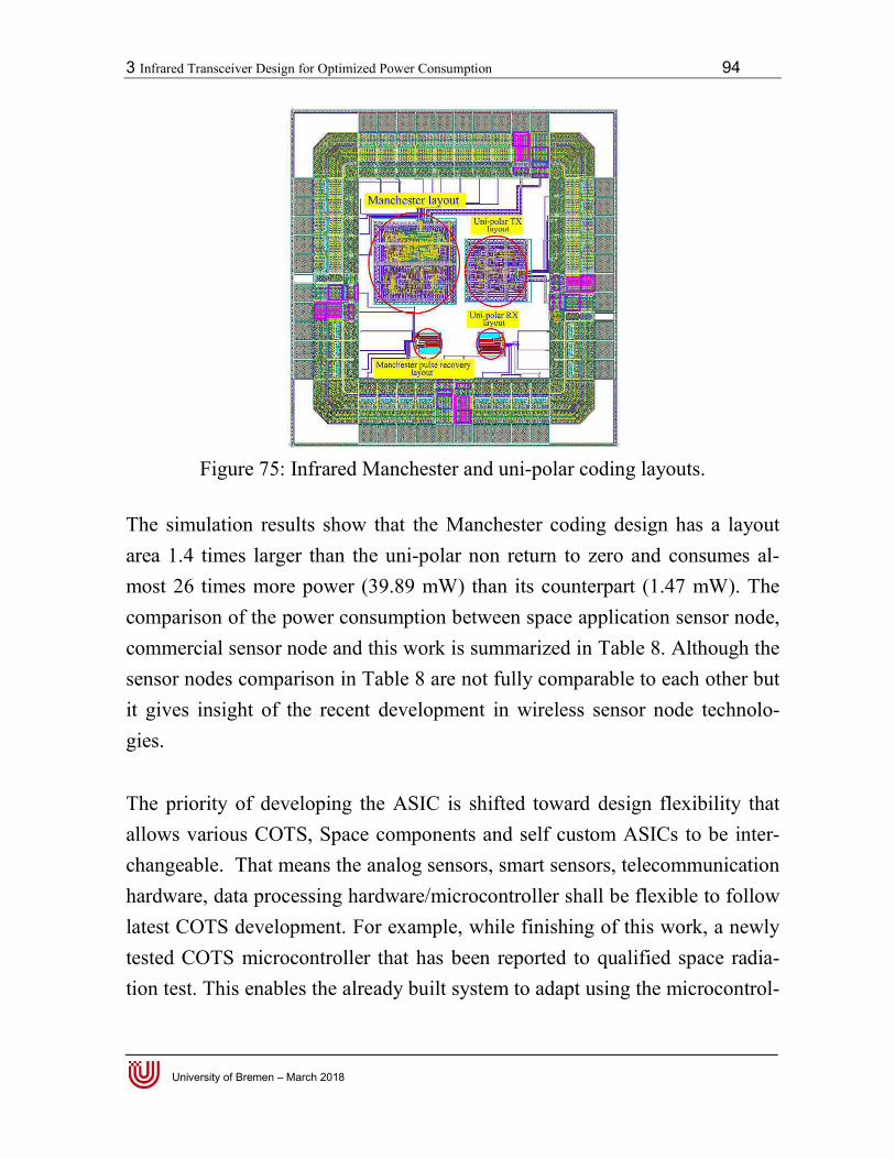
3 Infrared Transceiver Design for Optimized Power Consumption 94
University of Bremen – March 2018
Figure 75: Infrared Manchester and uni-polar coding layouts.
The simulation results show that the Manchester coding design has a layout area 1.4 times larger than the uni-polar non return to zero and consumes al-most 26 times more power (39.89 mW) than its counterpart (1.47 mW). The comparison of the power consumption between space application sensor node, commercial sensor node and this work is summarized in Table 8. Although the sensor nodes comparison in Table 8 are not fully comparable to each other but it gives insight of the recent development in wireless sensor node technolo-gies. The priority of developing the ASIC is shifted toward design flexibility that allows various COTS, Space components and self custom ASICs to be inter-changeable. That means the analog sensors, smart sensors, telecommunication hardware, data processing hardware/microcontroller shall be flexible to follow latest COTS development. For example, while finishing of this work, a newly tested COTS microcontroller that has been reported to qualified space radia-tion test. This enables the already built system to adapt using the microcontrol-
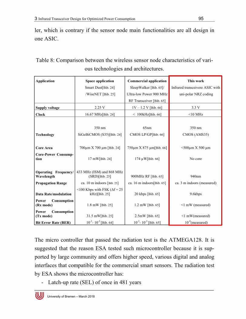
3 Infrared Transceiver Design for Optimized Power Consumption 95
University of Bremen – March 2018
ler, which is contrary if the sensor node main functionalities are all design in one ASIC.
Table 8: Comparison between the wireless sensor node characteristics of vari-ous technologies and architectures.
Application Space application Commercial application This work
Smart Dust[Bib. 24] SleepWalker [Bib. 65]/ Infrared transceivere ASIC with
/WiseNET [Bib. 25] Ultra-low Power 900 MHz uni-polar NRZ coding
RF Transceiver [Bib. 65]
Supply voltage 2.25 V 1V – 1.2 V [Bib. 66] 3.3 V
Clock 16.67 MHz[Bib. 24] < 100kHz[Bib. 66] <10 MHz
Technology
350 nm
SiGeBiCMOS (S35)[Bib. 24]
65nm
CMOS LP/GP[Bib. 66]
350 nm
CMOS (AMS35)
Core Area 700µm X 700 µm [Bib. 24] 750µm X 875 µm[Bib. 66] <500µm X 500 µm
Core-Power Consump-tion 17 mW[Bib. 24] 174 µW[Bib. 66] No core
Operating Frequency/ Wavelength
433 MHz (ISM) and 868 MHz (SRD)[Bib. 25] 900MHz RF [Bib. 65] 940nm
Propagation Range ca. 10 m indoors [Bib. 25] ca. 16 m indoors[Bib. 65] ca. 3 m indoors (measured)
Data Rate/modulation <100 Kbps with FSK (Δf = 25
kHz)[Bib. 25] 20 kbps [Bib. 65] 9.6kbps
Power Consumption (Rx mode) 1.8 mW [Bib. 25] 1.2 mW [Bib. 65] <1 mW (measured)
Power Consumption (Tx mode) 31.5 mW[Bib. 25] 2.5mW [Bib. 65] <1 mW(measured)
Bit Error Rate (BER) 10-3- 10-5 [Bib. 64] 10-3- 10-5 [Bib. 65] 10-9(measured)
The micro controller that passed the radiation test is the ATMEGA128. It is suggested that the reason ESA tested such microcontroller because it is sup-ported by large community and offers higher speed, various digital and analog interfaces that compatible for the commercial smart sensors. The radiation test by ESA shows the microcontroller has:
- Latch-up rate (SEL) of once in 481 years
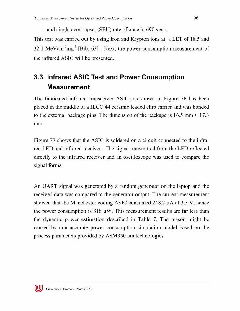
3 Infrared Transceiver Design for Optimized Power Consumption 96
University of Bremen – March 2018
- and single event upset (SEU) rate of once in 690 years
This test was carried out by using Iron and Krypton ions at a LET of 18.5 and
32.1 MeVcm-2mg-1 [Bib. 63] . Next, the power consumption measurement of
the infrared ASIC will be presented.
3.3 Infrared ASIC Test and Power Consumption Measurement
The fabricated infrared transceiver ASICs as shown in Figure 76 has been placed in the middle of a JLCC 44 ceramic leaded chip carrier and was bonded to the external package pins. The dimension of the package is 16.5 mm × 17.3 mm. Figure 77 shows that the ASIC is soldered on a circuit connected to the infra-red LED and infrared receiver. The signal transmitted from the LED reflected directly to the infrared receiver and an oscilloscope was used to compare the signal forms.
An UART signal was generated by a random generator on the laptop and the received data was compared to the generator output. The current measurement showed that the Manchester coding ASIC consumed 248.2 µA at 3.3 V, hence the power consumption is 818 µW. This measurement results are far less than the dynamic power estimation described in Table 7. The reason might be caused by non accurate power consumption simulation model based on the process parameters provided by ASM350 nm technologies.
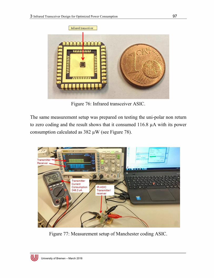
3 Infrared Transceiver Design for Optimized Power Consumption 97
University of Bremen – March 2018
Figure 76: Infrared transceiver ASIC.
The same measurement setup was prepared on testing the uni-polar non return to zero coding and the result shows that it consumed 116.8 µA with its power consumption calculated as 382 µW (see Figure 78).
Figure 77: Measurement setup of Manchester coding ASIC.
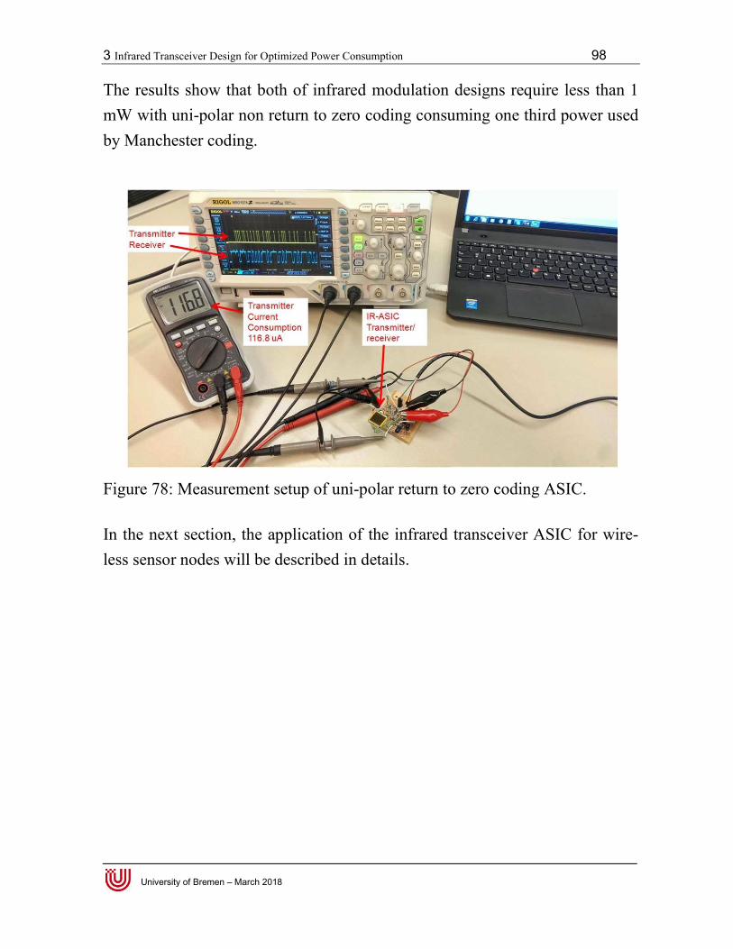
3 Infrared Transceiver Design for Optimized Power Consumption 98
University of Bremen – March 2018
The results show that both of infrared modulation designs require less than 1 mW with uni-polar non return to zero coding consuming one third power used by Manchester coding.
Figure 78: Measurement setup of uni-polar return to zero coding ASIC.
In the next section, the application of the infrared transceiver ASIC for wire-less sensor nodes will be described in details.
4 Infrared Wireless Sensor Node Implementation 99
University of Bremen – March 2018
4 Infrared Wireless Sensor Node Implementation
In this section the implementation of the sensor node in the VEB and the tests performed to meet the Ariane 5's requirements will be described:
4.1 Infrared Wireless Sensor Node Prototype for VEB
There have been many discussions to utilize wireless sensor networks (WSNs) in space applications. Several scenarios by using the available communication methods for various space applications are listed below: Autonomous formation flying (e.g. Scenario of measurement process of
an asteroid [Bib. 36])
Very small satellite cluster/swarm (e.g. ERMES nano satellite [Bib. 35],
ESPACENET [Bib. 37])
Segmented spacecraft
On board sensor network
Surface vehicles on moon, planets and asteroids
Table 9 describes the criteria of potential communication technologies for space-based WSNs. The symbols “++, +, o, - , - - ” summarize the degree of COTS technology applicability for the WSN.
For the segmented spacecraft like Ariane 5, the wireless energy transfer and clock synchronization are key issues on applying COTS technologies. Al-though the RFID technology for aerospace application was investigated by NASA for such purpose [Ref. 63], the development of wireless transfer and clock synchronization for a large segmented spacecraft like Ariane 5 mainly is carried out by ESA in the frame of this work.
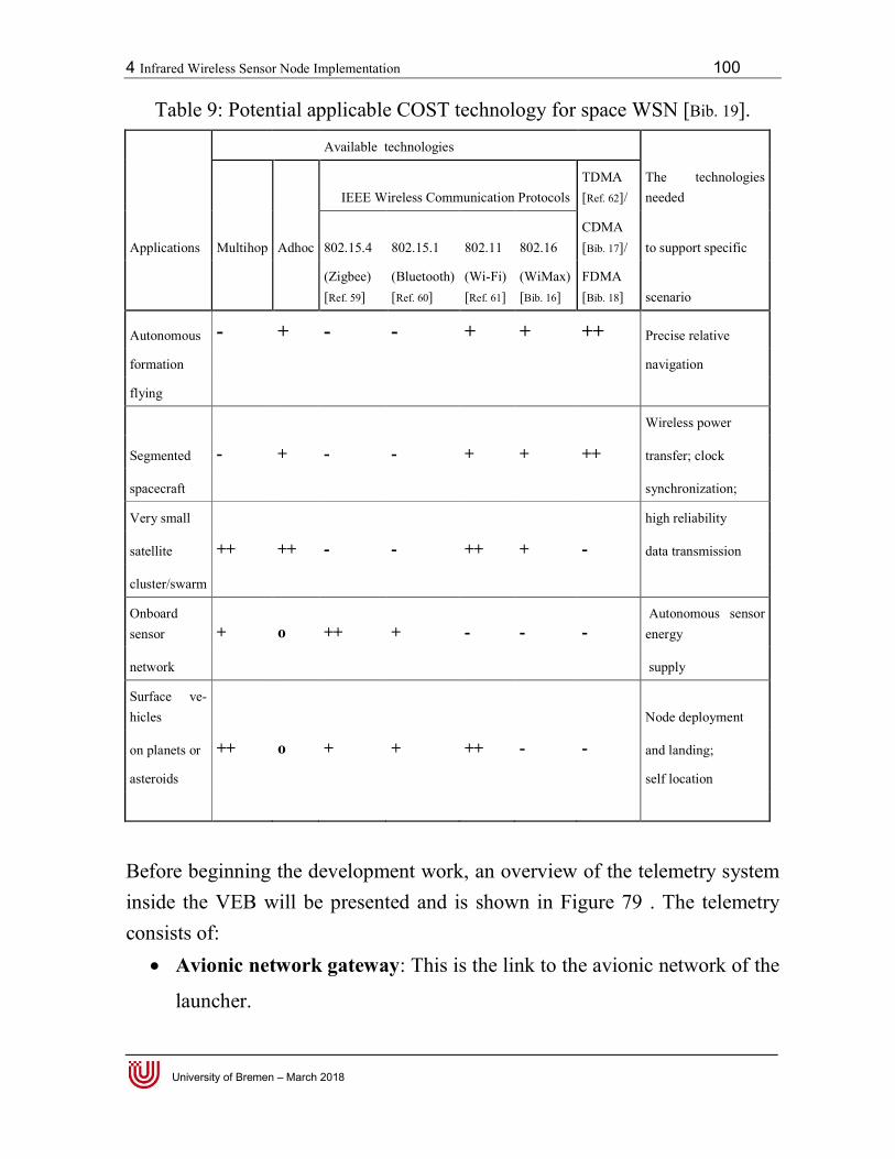
4 Infrared Wireless Sensor Node Implementation 100
University of Bremen – March 2018
Table 9: Potential applicable COST technology for space WSN [Bib. 19].
Available technologies
IEEE Wireless Communication Protocols TDMA [Ref. 62]/
The technologies needed
Applications Multihop Adhoc 802.15.4 802.15.1 802.11 802.16 CDMA [Bib. 17]/ to support specific
(Zigbee) [Ref. 59]
(Bluetooth) [Ref. 60]
(Wi-Fi) [Ref. 61]
(WiMax) [Bib. 16]
FDMA [Bib. 18] scenario
Autonomous - + - - + + ++ Precise relative
formation navigation
flying
Wireless power
Segmented - + - - + + ++ transfer; clock
spacecraft synchronization;
Very small high reliability
satellite ++ ++ - - ++ + - data transmission
cluster/swarm
Onboard sensor + o ++ + - - -
Autonomous sensor energy
network supply
Surface ve-hicles Node deployment
on planets or ++ o + + ++ - - and landing;
asteroids self location
Before beginning the development work, an overview of the telemetry system inside the VEB will be presented and is shown in Figure 79 . The telemetry consists of: Avionic network gateway: This is the link to the avionic network of the
launcher.

4 Infrared Wireless Sensor Node Implementation
University of Bremen – March 2018
Data concentrator: The information traffic and measurement sequences
from different kind of networks are managed in this layer.
Plain old sensors: analog space qualified sensors.
Smart sensors: smart sensors for future application.
UWB sensor network
Infrared wireless sensor network
Figure 79: Space Telemetry Network
The infrared wireless sensor network is part of the telemetry system and rquires sensor nodes and access points to operate. The chance was given to iplement the infrared transceiver ASIC and therefore to demonstrate its wirless communication ability in the a low power sensor node that consists of analog and digital sensors implemented. The steps of developments are described in details as following:
Wireless Sensor Node Implementation
: The information traffic and measurement sequences
from different kind of networks are managed in this layer.
: analog space qualified sensors.
: smart sensors for future application.
UWB sensor network: was investigated in other work.
Infrared wireless sensor network: focus of this work.
: Space Telemetry Network proposed for Ariane 5's VEB [
infrared wireless sensor network is part of the telemetry system and rquires sensor nodes and access points to operate. The chance was given to iplement the infrared transceiver ASIC and therefore to demonstrate its wirless communication ability in the network. As mentioned in the objectives of, a low power sensor node that consists of analog and digital sensors
he steps of developments are described in details as following:
101
: The information traffic and measurement sequences
VEB [Bib. 20].
infrared wireless sensor network is part of the telemetry system and re-quires sensor nodes and access points to operate. The chance was given to im-plement the infrared transceiver ASIC and therefore to demonstrate its wire-
network. As mentioned in the objectives of, a low power sensor node that consists of analog and digital sensors shall be
he steps of developments are described in details as following:
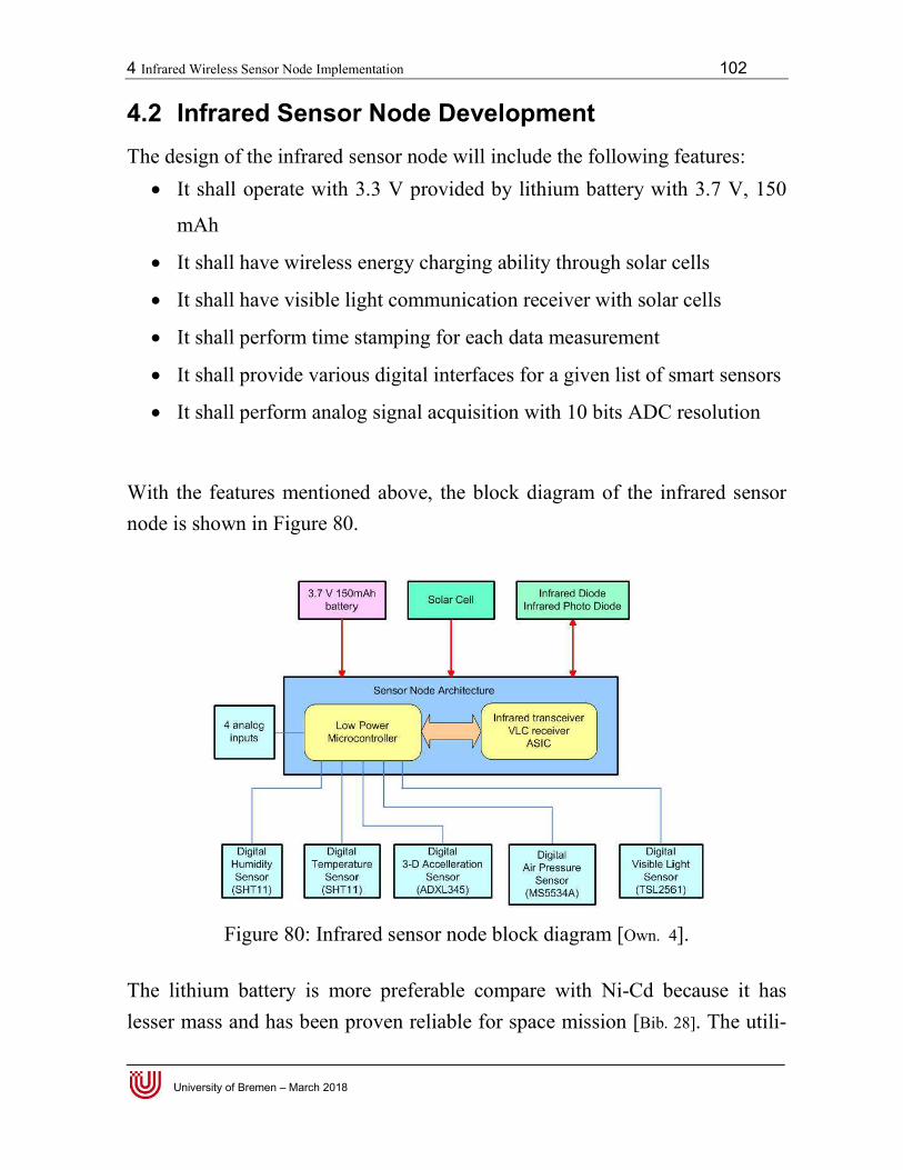
4 Infrared Wireless Sensor Node Implementation
University of Bremen – March 2018
4.2 Infrared Sensor Node DevelopmentThe design of the infrared sensor node will include the following features: It shall operate with 3.3 V
mAh
It shall have wireless energy charging
It shall have visible light communication
It shall perform time stamping for each data measurement
It shall provide various digital interfaces for a given list of smart sensors
It shall perform analog signal acquisition with 10 bits ADC resolution
With the features mentioned above, the blnode is shown in Figure 80.
Figure 80: Infrared sensor node block diagram [
The lithium battery is more preferable compare with Nilesser mass and has been proven reliable
Wireless Sensor Node Implementation
Infrared Sensor Node Development ed sensor node will include the following features:
operate with 3.3 V provided by lithium battery with 3.7 V
have wireless energy charging ability through solar cells
visible light communication receiver with solar
perform time stamping for each data measurement
provide various digital interfaces for a given list of smart sensors
perform analog signal acquisition with 10 bits ADC resolution
With the features mentioned above, the block diagram of the infrared sensor .
: Infrared sensor node block diagram [Own. 4
ore preferable compare with Ni-Cd because it has proven reliable for space mission [Bib. 28
102
ed sensor node will include the following features: lithium battery with 3.7 V, 150
through solar cells
solar cells
provide various digital interfaces for a given list of smart sensors
perform analog signal acquisition with 10 bits ADC resolution
ock diagram of the infrared sensor
4].
Cd because it has 28]. The utili-

4 Infrared Wireless Sensor Node Implementation 103
University of Bremen – March 2018
zation of the lithium battery for space technology has been performed by NASA and was successfully completed in 2005 [Bib. 29]. A PCB was designed for the sensors and infrared transceivers’ component and shown in Figure 81. This arrangement is compact in size compare with typical outdoor sensor node design[Bib. 32]. To increase the coverage area, infrared LEDs and receivers are located in four directions. The transceiver AS-IC was placed in the centre of the PCB with the smart sensors surrounding it.
Figure 81: Infrared wireless sensor node [Own. 4].
All sensors were tested and each sensor measurement period including ADC was recorded and is listed in Table 10. This information tells how long each sensor performs the measurement and therefore can be used to calculate the times needed for the time stamping algorithm.
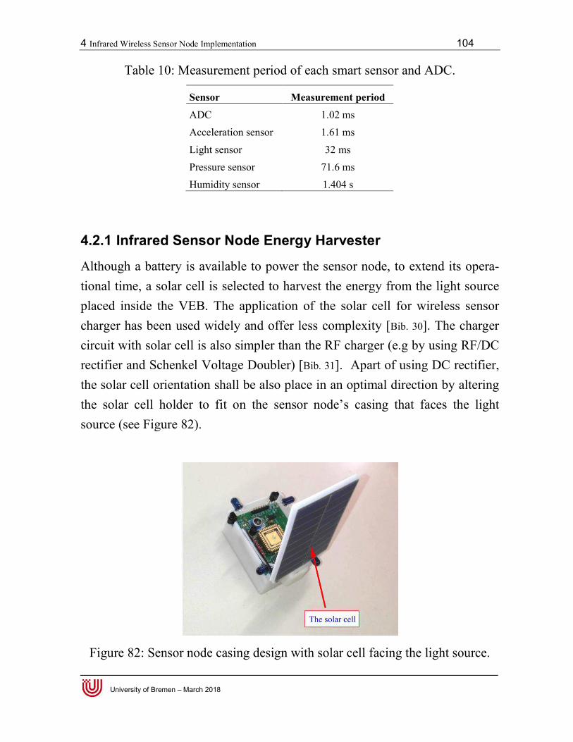
4 Infrared Wireless Sensor Node Implementation 104
University of Bremen – March 2018
Table 10: Measurement period of each smart sensor and ADC.
Sensor Measurement period ADC 1.02 ms
Acceleration sensor 1.61 ms
Light sensor 32 ms
Pressure sensor 71.6 ms
Humidity sensor 1.404 s
4.2.1 Infrared Sensor Node Energy Harvester
Although a battery is available to power the sensor node, to extend its opera-tional time, a solar cell is selected to harvest the energy from the light source placed inside the VEB. The application of the solar cell for wireless sensor charger has been used widely and offer less complexity [Bib. 30]. The charger circuit with solar cell is also simpler than the RF charger (e.g by using RF/DC rectifier and Schenkel Voltage Doubler) [Bib. 31]. Apart of using DC rectifier, the solar cell orientation shall be also place in an optimal direction by altering the solar cell holder to fit on the sensor node’s casing that faces the light source (see Figure 82).
Figure 82: Sensor node casing design with solar cell facing the light source.
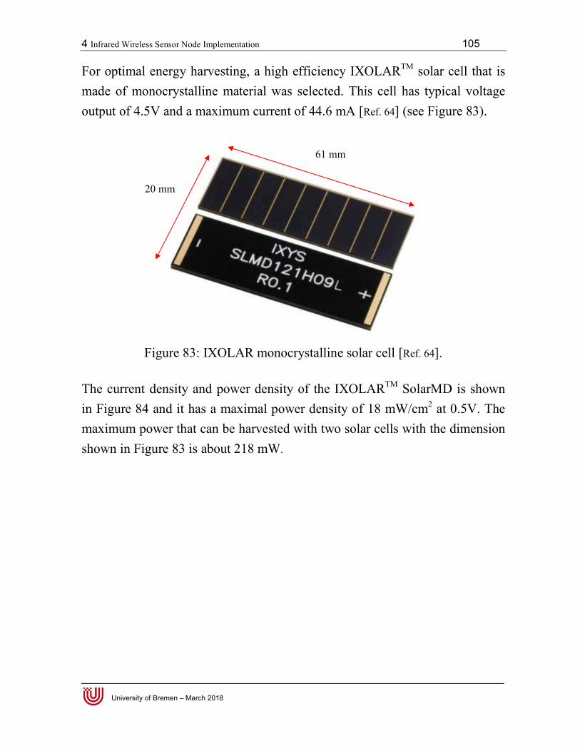
4 Infrared Wireless Sensor Node Implementation 105
University of Bremen – March 2018
For optimal energy harvesting, a high efficiency IXOLARTM solar cell that is made of monocrystalline material was selected. This cell has typical voltage output of 4.5V and a maximum current of 44.6 mA [Ref. 64] (see Figure 83).
Figure 83: IXOLAR monocrystalline solar cell [Ref. 64].
The current density and power density of the IXOLARTM SolarMD is shown in Figure 84 and it has a maximal power density of 18 mW/cm2 at 0.5V. The maximum power that can be harvested with two solar cells with the dimension shown in Figure 83 is about 218 mW.
20 mm
61 mm
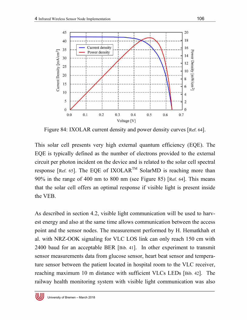
4 Infrared Wireless Sensor Node Implementation 106
University of Bremen – March 2018
Figure 84: IXOLAR current density and power density curves [Ref. 64].
This solar cell presents very high external quantum efficiency (EQE). The EQE is typically defined as the number of electrons provided to the external circuit per photon incident on the device and is related to the solar cell spectral response [Ref. 65]. The EQE of IXOLARTM SolarMD is reaching more than 90% in the range of 400 nm to 800 nm (see Figure 85) [Ref. 64]. This means that the solar cell offers an optimal response if visible light is present inside the VEB. As described in section 4.2, visible light communication will be used to harv-est energy and also at the same time allows communication between the access point and the sensor nodes. The measurement performed by H. Hematkhah et al. with NRZ-OOK signaling for VLC LOS link can only reach 150 cm with 2400 baud for an acceptable BER [Bib. 41]. In other experiment to transmit sensor measurements data from glucose sensor, heart beat sensor and tempera-ture sensor between the patient located in hospital room to the VLC receiver, reaching maximum 10 m distance with sufficient VLCs LEDs [Bib. 42]. The railway health monitoring system with visible light communication was also
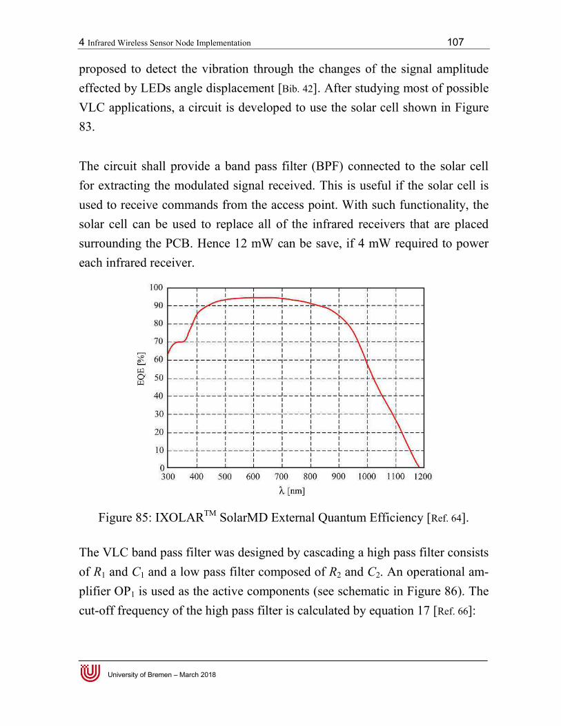
4 Infrared Wireless Sensor Node Implementation 107
University of Bremen – March 2018
proposed to detect the vibration through the changes of the signal amplitude effected by LEDs angle displacement [Bib. 42]. After studying most of possible VLC applications, a circuit is developed to use the solar cell shown in Figure 83. The circuit shall provide a band pass filter (BPF) connected to the solar cell for extracting the modulated signal received. This is useful if the solar cell is used to receive commands from the access point. With such functionality, the solar cell can be used to replace all of the infrared receivers that are placed surrounding the PCB. Hence 12 mW can be save, if 4 mW required to power each infrared receiver.
Figure 85: IXOLARTM SolarMD External Quantum Efficiency [Ref. 64].
The VLC band pass filter was designed by cascading a high pass filter consists of R1 and C1 and a low pass filter composed of R2 and C2. An operational am-plifier OP1 is used as the active components (see schematic in Figure 86). The cut-off frequency of the high pass filter is calculated by equation 17 [Ref. 66]:
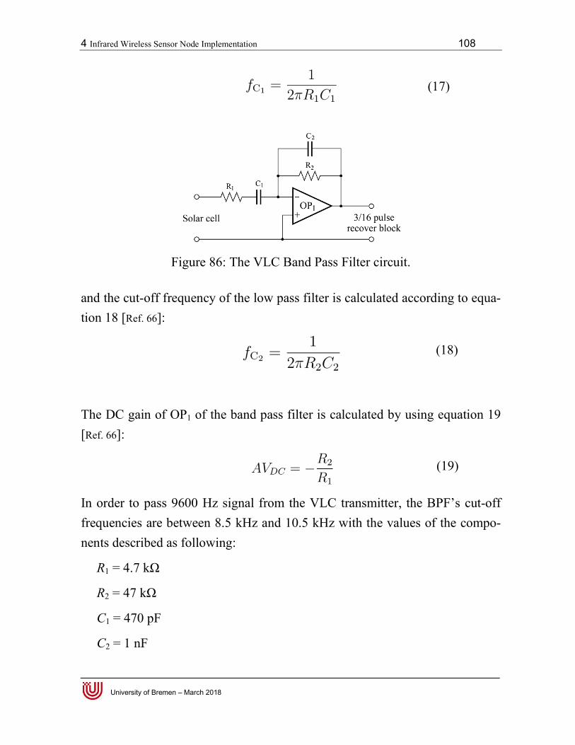
4 Infrared Wireless Sensor Node Implementation 108
University of Bremen – March 2018
Figure 86: The VLC Band Pass Filter circuit.
and the cut-off frequency of the low pass filter is calculated according to equa-tion 18 [Ref. 66]:
The DC gain of OP1 of the band pass filter is calculated by using equation 19 [Ref. 66]:
In order to pass 9600 Hz signal from the VLC transmitter, the BPF’s cut-off frequencies are between 8.5 kHz and 10.5 kHz with the values of the compo-nents described as following:
R1 = 4.7 kΩ
R2 = 47 kΩ
C1 = 470 pF
C2 = 1 nF
(17)
(18)
(19)

4 Infrared Wireless Sensor Node Implementation 109
University of Bremen – March 2018
The active component OP1 is LT1006 single supply operational amplifier that delivers low offset voltage 50 µV and a power consumption of less than 340 µW [Ref. 67]. Figure 87 shows the simulation results of the BPF gain by using the values of the components obtained from equation 18 and 19. The results simulated with LT1006 LTSPICE model shows tendency of a HPF gain. At the graph, the cut-off frequency is found at 10 kHz with maximum gain -25 dB. Although the realization of the circuit works fine with the solar cell, but many attempts were carried out to find optimal gain. As an example by varying the compo-nents values through LTSPICE parameters sweep. To obtain narrow Q value by using only one active filter stage is very challenging. The solution to keep high Q at narrow band width 2 kHz with resonant frequency 9600 Hz is nor-mally done by adding more filter stages. But this might lead to higher circuit complexity and more energy consumption.
Figure 87: BPF gain and phase simulation with LT-Spice.
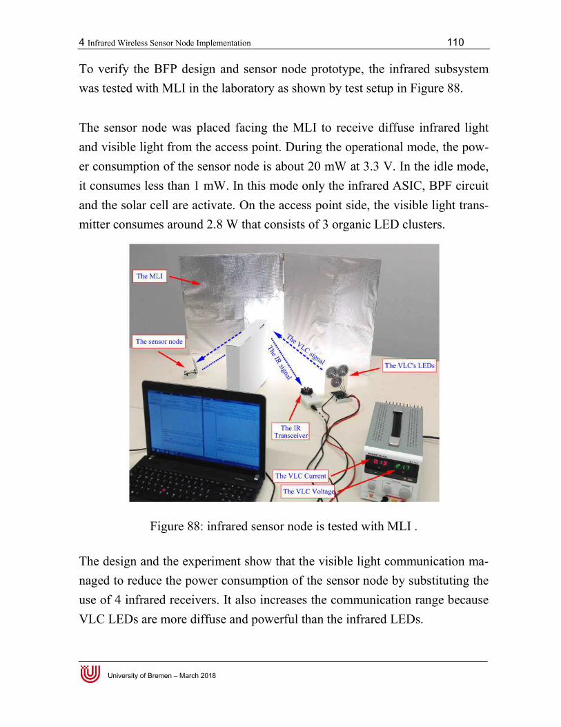
4 Infrared Wireless Sensor Node Implementation 110
University of Bremen – March 2018
To verify the BFP design and sensor node prototype, the infrared subsystem was tested with MLI in the laboratory as shown by test setup in Figure 88. The sensor node was placed facing the MLI to receive diffuse infrared light and visible light from the access point. During the operational mode, the pow-er consumption of the sensor node is about 20 mW at 3.3 V. In the idle mode, it consumes less than 1 mW. In this mode only the infrared ASIC, BPF circuit and the solar cell are activate. On the access point side, the visible light trans-mitter consumes around 2.8 W that consists of 3 organic LED clusters.
Figure 88: infrared sensor node is tested with MLI .
The design and the experiment show that the visible light communication ma-naged to reduce the power consumption of the sensor node by substituting the use of 4 infrared receivers. It also increases the communication range because VLC LEDs are more diffuse and powerful than the infrared LEDs.
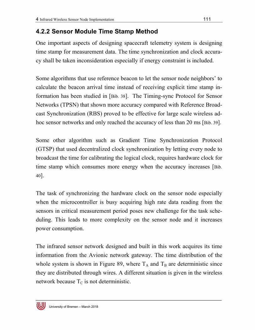
4 Infrared Wireless Sensor Node Implementation 111
University of Bremen – March 2018
4.2.2 Sensor Module Time Stamp Method
One important aspects of designing spacecraft telemetry system is designing time stamp for measurement data. The time synchronization and clock accura-cy shall be taken inconsideration especially if energy constraint is included. Some algorithms that use reference beacon to let the sensor node neighbors’ to calculate the beacon arrival time instead of receiving explicit time stamp in-formation has been studied in [Bib. 38]. The Timing-sync Protocol for Sensor Networks (TPSN) that shown more accuracy compared with Reference Broad-cast Synchronization (RBS) proved to be effective for large scale wireless ad-hoc sensor networks and only reached the accuracy of less than 20 ms [Bib. 39]. Some other algorithm such as Gradient Time Synchronization Protocol (GTSP) that used decentralized clock synchronization by letting every node to broadcast the time for calibrating the logical clock, requires hardware clock for time stamp which consumes more energy when the accuracy increases [Bib.
40]. The task of synchronizing the hardware clock on the sensor node especially when the microcontroller is busy acquiring high rate data reading from the sensors in critical measurement period poses new challenge for the task sche-duling. This leads to more complexity on the sensor node and it increases power consumption. The infrared sensor network designed and built in this work acquires its time information from the Avionic network gateway. The time distribution of the whole system is shown in Figure 89, where TA and TB are deterministic since they are distributed through wires. A different situation is given in the wireless network because TC is not deterministic.
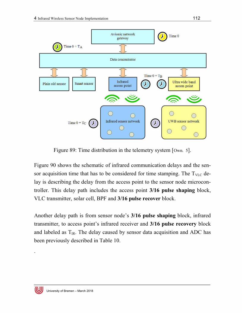
4 Infrared Wireless Sensor Node Implementation 112
University of Bremen – March 2018
Figure 89: Time distribution in the telemetry system [Own. 5].
Figure 90 shows the schematic of infrared communication delays and the sen-sor acquisition time that has to be considered for time stamping. The TVLC de-lay is describing the delay from the access point to the sensor node microcon-troller. This delay path includes the access point 3/16 pulse shaping block, VLC transmitter, solar cell, BPF and 3/16 pulse recover block. Another delay path is from sensor node’s 3/16 pulse shaping block, infrared transmitter, to access point’s infrared receiver and 3/16 pulse recovery block and labeled as TIR. The delay caused by sensor data acquisition and ADC has been previously described in Table 10.
.

4 Infrared Wireless Sensor Node Implementation 113
University of Bremen – March 2018
Figure 90: The infrared network communication delay and sensor acquisition time diagram.
In order to reduce the complexity and computational power, the time stamp activity is concentrated in the access point. This is justified since access point has higher computational power than sensor node and does not have energy constraints. On the other hand, the power consumption of the sensor node can be reduced by eliminating the use of real time clock hardware. The realization of this design is by subtracting the current time T0 with the infrared communi-cation delay TIR when the data is received by the access point.
The delay in the infrared communication for time stamp is shown in Figure 91.
Where Table 11 listed the communication latency (TVLC + Tsensor + TIR) and is mainly affected by the processing time of various smart sensors.
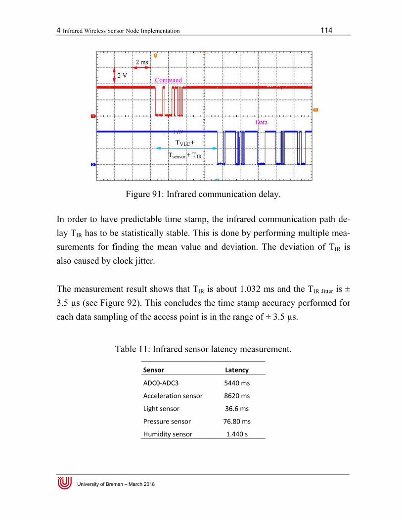
4 Infrared Wireless Sensor Node Implementation 114
University of Bremen – March 2018
Figure 91: Infrared communication delay.
In order to have predictable time stamp, the infrared communication path de-lay TIR has to be statistically stable. This is done by performing multiple mea-surements for finding the mean value and deviation. The deviation of TIR is also caused by clock jitter. The measurement result shows that TIR is about 1.032 ms and the TIR Jitter is ± 3.5 µs (see Figure 92). This concludes the time stamp accuracy performed for each data sampling of the access point is in the range of ± 3.5 µs.
Table 11: Infrared sensor latency measurement.
Sensor Latency
ADC0-ADC3 5440 ms
Acceleration sensor 8620 ms
Light sensor 36.6 ms
Pressure sensor 76.80 ms
Humidity sensor 1.440 s
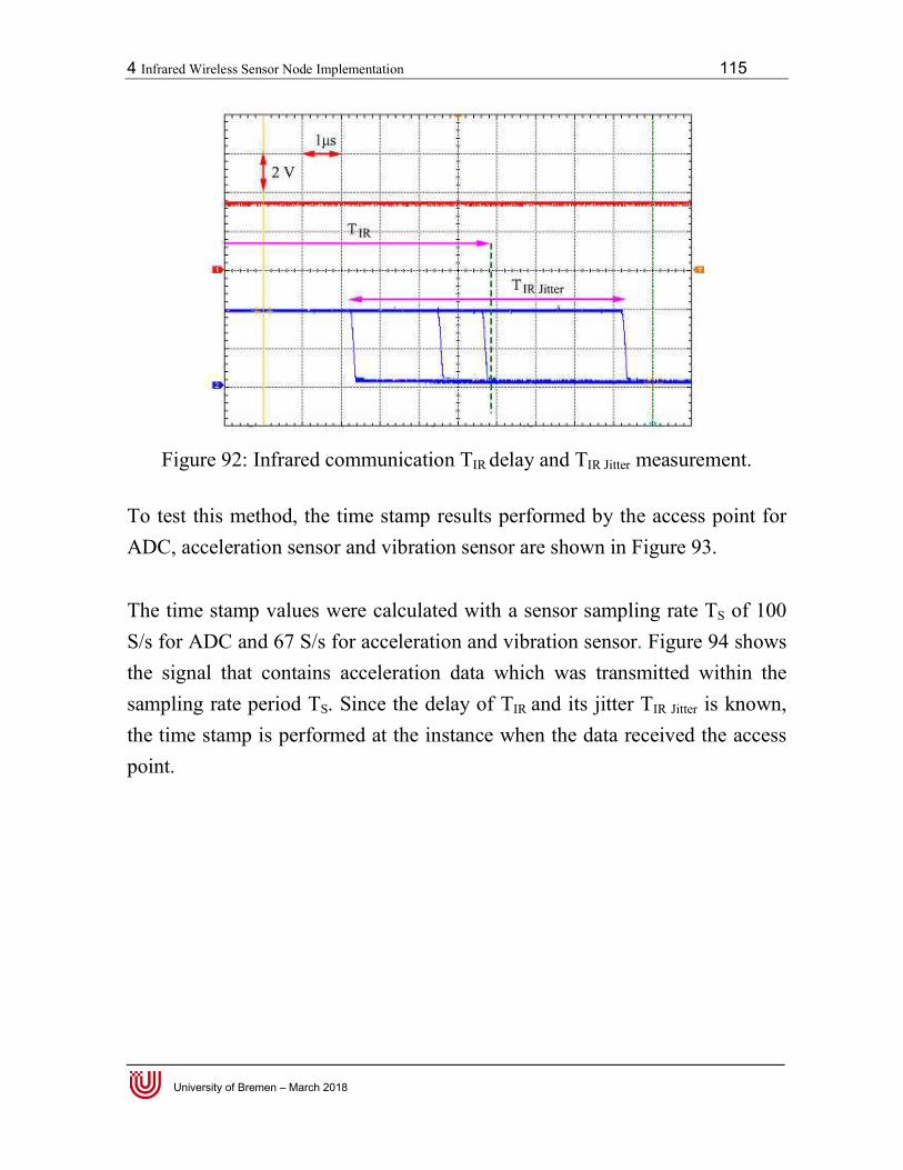
4 Infrared Wireless Sensor Node Implementation 115
University of Bremen – March 2018
Figure 92: Infrared communication TIR delay and TIR Jitter measurement.
To test this method, the time stamp results performed by the access point for ADC, acceleration sensor and vibration sensor are shown in Figure 93. The time stamp values were calculated with a sensor sampling rate TS of 100 S/s for ADC and 67 S/s for acceleration and vibration sensor. Figure 94 shows the signal that contains acceleration data which was transmitted within the sampling rate period TS. Since the delay of TIR and its jitter TIR Jitter is known, the time stamp is performed at the instance when the data received the access point.

4 Infrared Wireless Sensor Node Implementation 116
University of Bremen – March 2018
Figure 93: Time stamp result performed at the access point.
Figure 94: Acceleration sensor sampling rate signal measurement.
Time stamp
Data
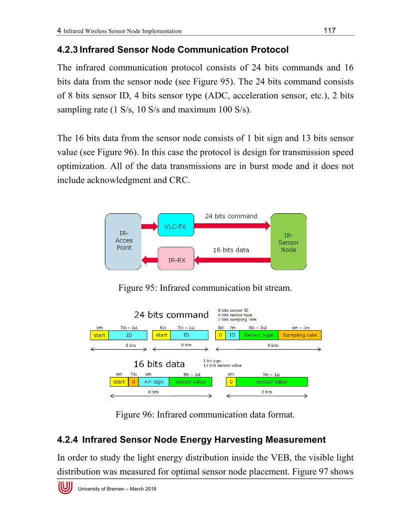
4 Infrared Wireless Sensor Node Implementation 117
University of Bremen – March 2018
4.2.3 Infrared Sensor Node Communication Protocol
The infrared communication protocol consists of 24 bits commands and 16 bits data from the sensor node (see Figure 95). The 24 bits command consists of 8 bits sensor ID, 4 bits sensor type (ADC, acceleration sensor, etc.), 2 bits sampling rate (1 S/s, 10 S/s and maximum 100 S/s). The 16 bits data from the sensor node consists of 1 bit sign and 13 bits sensor value (see Figure 96). In this case the protocol is design for transmission speed optimization. All of the data transmissions are in burst mode and it does not include acknowledgment and CRC.
Figure 95: Infrared communication bit stream.
Figure 96: Infrared communication data format.
4.2.4 Infrared Sensor Node Energy Harvesting Measurement
In order to study the light energy distribution inside the VEB, the visible light distribution was measured for optimal sensor node placement. Figure 97 shows
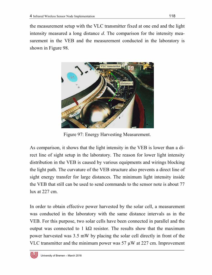
4 Infrared Wireless Sensor Node Implementation
University of Bremen – March 2018
the measurement setup with the VLC transmitter fixed at one end and the light intensity measured a long distance surement in the VEB and the measurement conducted in the laboratory is shown in Figure 98.
Figure 97: Energy Harvesting Measurement.
As comparison, it shows that the light intensity in the VEB is lower than a drect line of sight setup in the laboratory. The reason for lower light indistribution in the VEB is caused by various equipments and wirings blocking the light path. The curvature of the VEB structure also prevents a direct line of sight energy transfer for large distances. The minimum light intensity inside the VEB that still can be used to send commands to the sensor note is about 77 lux at 227 cm. In order to obtain effectivewas conducted in the laboratory with the same distance intervals as in the VEB. For this purpose, two solar cells have been connected in parallel and the output was connected to 1 kpower harvested was 3.5 mW by placing the solar cell directly in front of the VLC transmitter and the minimum power was 57 µW at 227 cm. Improvement
Wireless Sensor Node Implementation
the measurement setup with the VLC transmitter fixed at one end and the light distance d. The comparison for the intensity me
surement in the VEB and the measurement conducted in the laboratory is
: Energy Harvesting Measurement.
that the light intensity in the VEB is lower than a drect line of sight setup in the laboratory. The reason for lower light indistribution in the VEB is caused by various equipments and wirings blocking the light path. The curvature of the VEB structure also prevents a direct line of sight energy transfer for large distances. The minimum light intensity inside
t still can be used to send commands to the sensor note is about 77
effective power harvested by the solar cell, a measurement was conducted in the laboratory with the same distance intervals as in the
se, two solar cells have been connected in parallel and the output was connected to 1 kΩ resistor. The results show that the maximum power harvested was 3.5 mW by placing the solar cell directly in front of the VLC transmitter and the minimum power was 57 µW at 227 cm. Improvement
118
the measurement setup with the VLC transmitter fixed at one end and the light . The comparison for the intensity mea-
surement in the VEB and the measurement conducted in the laboratory is
that the light intensity in the VEB is lower than a di-rect line of sight setup in the laboratory. The reason for lower light intensity distribution in the VEB is caused by various equipments and wirings blocking the light path. The curvature of the VEB structure also prevents a direct line of sight energy transfer for large distances. The minimum light intensity inside
t still can be used to send commands to the sensor note is about 77
power harvested by the solar cell, a measurement was conducted in the laboratory with the same distance intervals as in the
se, two solar cells have been connected in parallel and the resistor. The results show that the maximum
power harvested was 3.5 mW by placing the solar cell directly in front of the VLC transmitter and the minimum power was 57 µW at 227 cm. Improvement
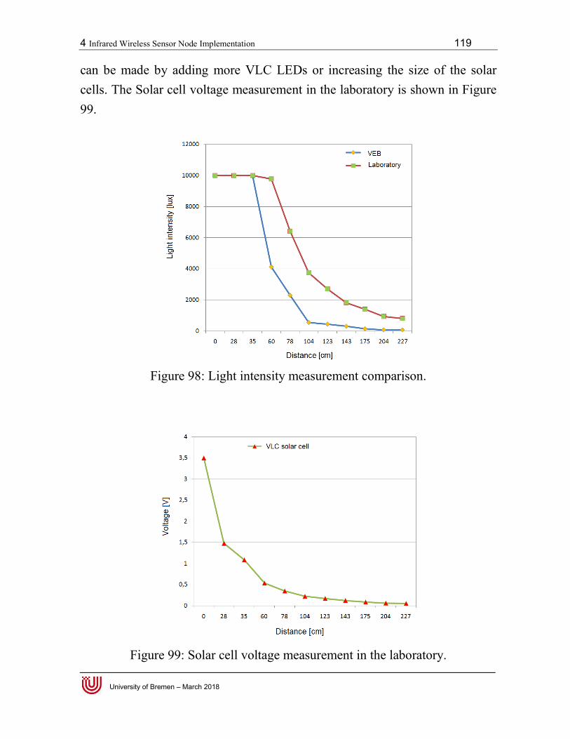
4 Infrared Wireless Sensor Node Implementation 119
University of Bremen – March 2018
can be made by adding more VLC LEDs or increasing the size of the solar cells. The Solar cell voltage measurement in the laboratory is shown in Figure 99.
Figure 98: Light intensity measurement comparison.
Figure 99: Solar cell voltage measurement in the laboratory.

4 Infrared Wireless Sensor Node Implementation 120
University of Bremen – March 2018
In the next section, the engineering test of the sensor node will be described in detail. The tests include mechanical tests, temperature tests and electromagnet-ic interference tests.
4.3 Infrared Sensor Node Engineering Tests
The engineering test is required to ensure the basic performance of the proto-type to fulfill the given specification. The tests of this section were carried out to identify design weakness affected by the space environment such as vibra-tion, shock, temperature shock and electromagnetic interferences. The test re-ports are still evaluated by European Space Agency at the moment of writing this dissertation and cannot be disclosed to the public.
4.3.1 Sensor Module Mechanical Tests
In order to survive the mechanical tests, the sensor node casing and PCB were redesigned (see Figure 100). The casing was designed to fit the vibration and shock test interface provided by the German Aerospace Centre. The casing of the infrared receiver and VLC transmitter were also redesigned and are shown in Figure 101.
Figure 100: Infrared sensor node redesigned casing and PCB.

4 Infrared Wireless Sensor Node Implementation 121
University of Bremen – March 2018
Figure 101: Infrared receiver and VLC transmitter redesigned casings.
The shaker available at the German Aerospace Centre test facilities has the ca-pability of [Ref. 68]: Maximum 150 g acceleration
Maximum speed of 1.8 m/s
Shaker frequency range 2 Hz to 6000 Hz
Maximum test object mass of 150 kg
The test equipment is shown in Figure 102 and the infrared sensor node instal-lation on the shaker in shown in Figure 103. At first, the sensor node is placed and fastened on the shaker structure interface. Several test sensors are place on various surface of the sensor node’s casing to monitor the sinusoidal wave and record the data for further analysis.
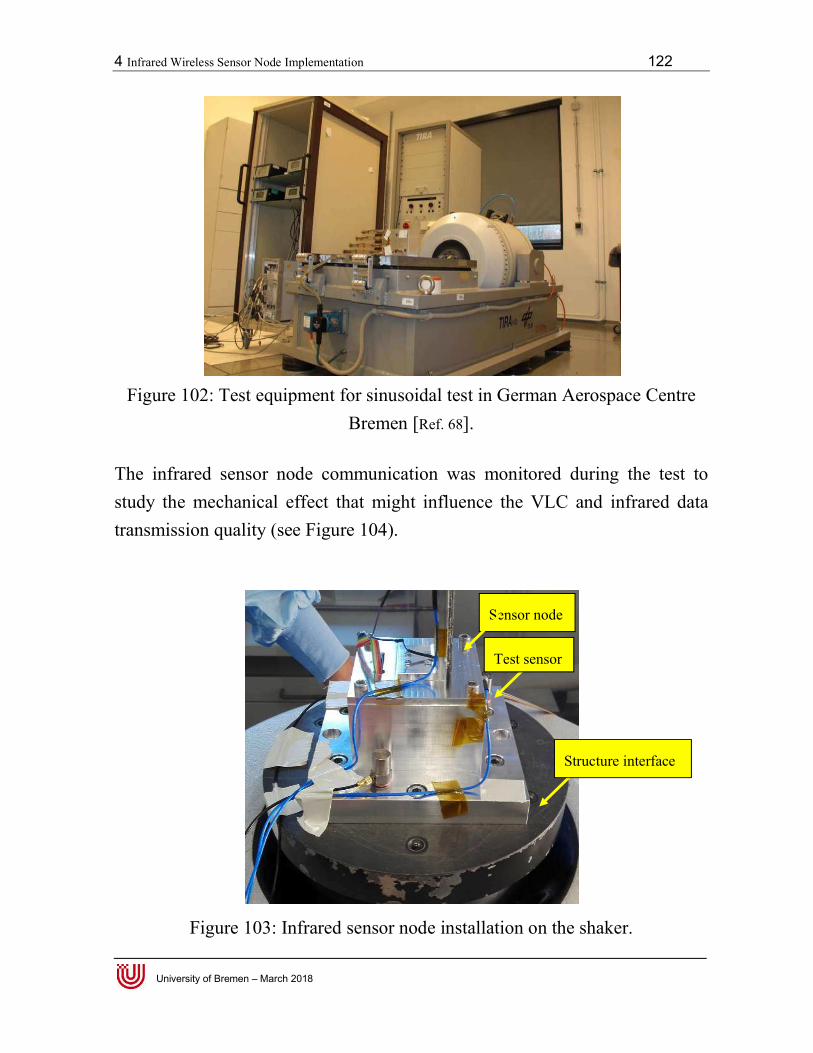
4 Infrared Wireless Sensor Node Implementation 122
University of Bremen – March 2018
Figure 102: Test equipment for sinusoidal test in German Aerospace Centre Bremen [Ref. 68].
The infrared sensor node communication was monitored during the test to study the mechanical effect that might influence the VLC and infrared data transmission quality (see Figure 104).
Figure 103: Infrared sensor node installation on the shaker.
Structure interface
Test sensor
Sensor node
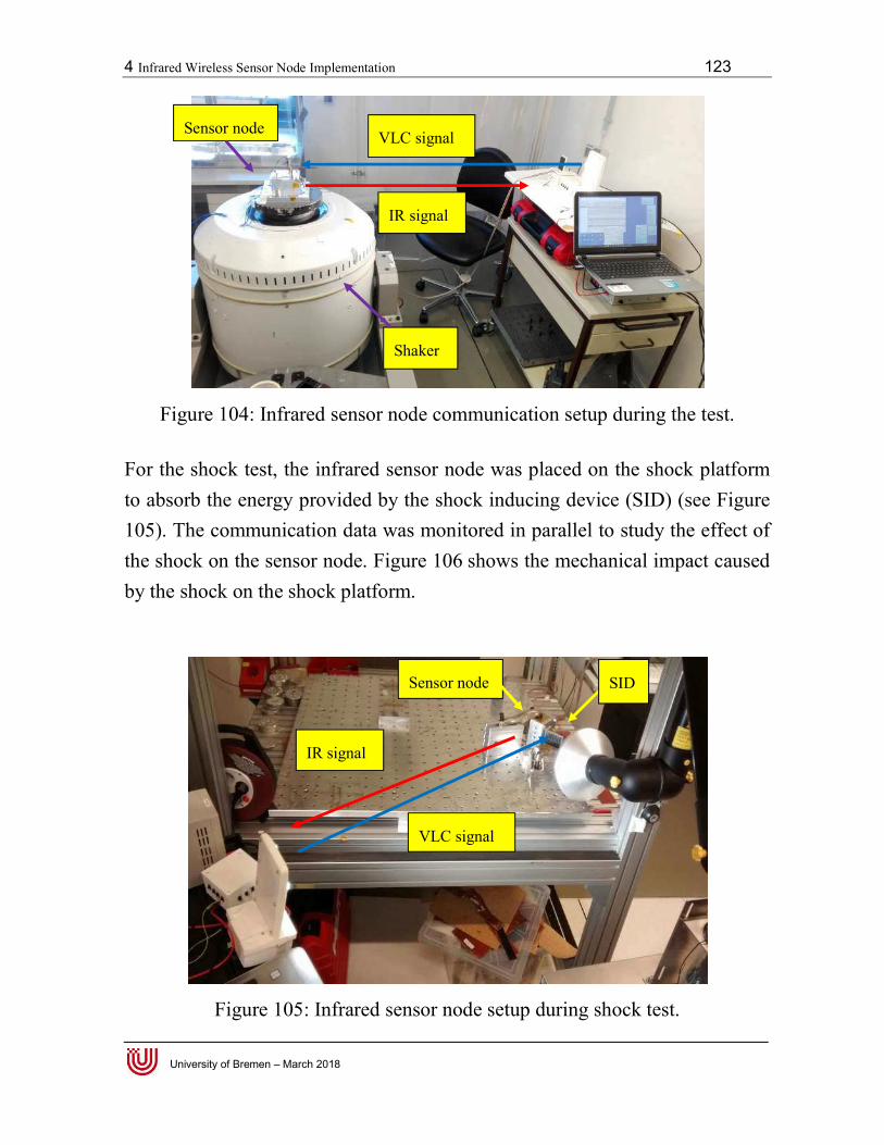
4 Infrared Wireless Sensor Node Implementation 123
University of Bremen – March 2018
Figure 104: Infrared sensor node communication setup during the test.
For the shock test, the infrared sensor node was placed on the shock platform to absorb the energy provided by the shock inducing device (SID) (see Figure 105). The communication data was monitored in parallel to study the effect of the shock on the sensor node. Figure 106 shows the mechanical impact caused by the shock on the shock platform.
Figure 105: Infrared sensor node setup during shock test.
IR signal
VLC signal Sensor node
Shaker
SID Sensor node
VLC signal
IR signal
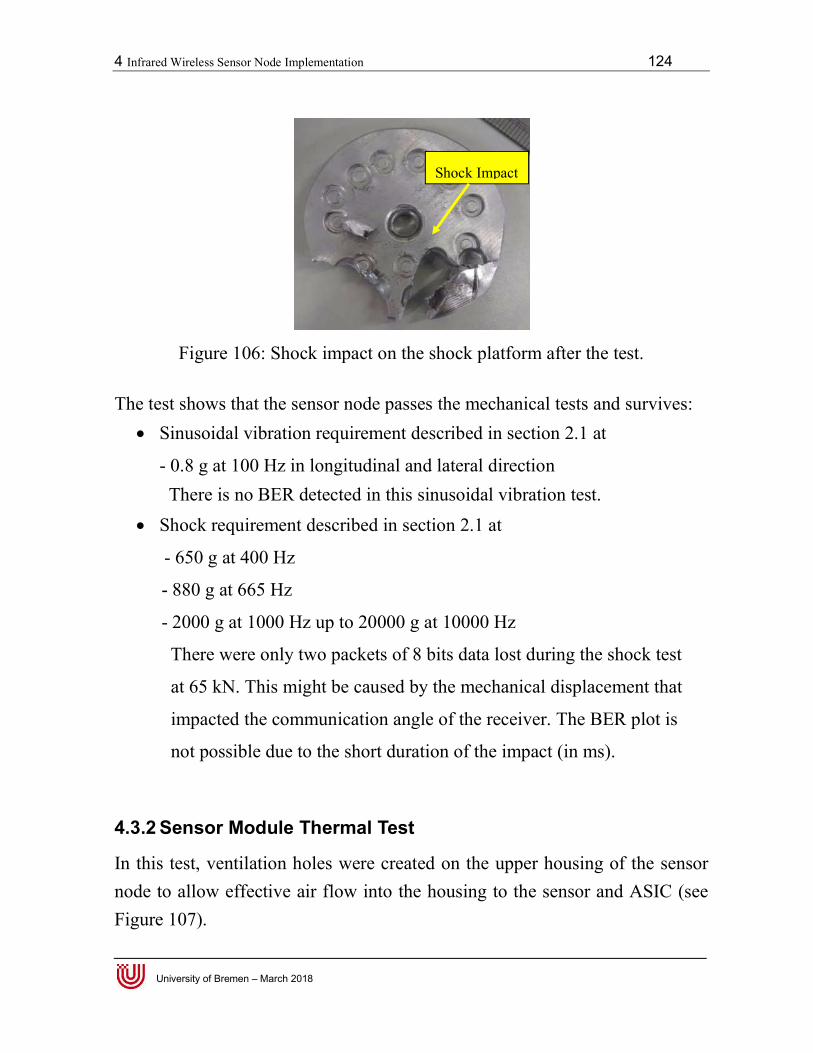
4 Infrared Wireless Sensor Node Implementation 124
University of Bremen – March 2018
Figure 106: Shock impact on the shock platform after the test.
The test shows that the sensor node passes the mechanical tests and survives: Sinusoidal vibration requirement described in section 2.1 at
- 0.8 g at 100 Hz in longitudinal and lateral direction There is no BER detected in this sinusoidal vibration test.
Shock requirement described in section 2.1 at
- 650 g at 400 Hz
- 880 g at 665 Hz
- 2000 g at 1000 Hz up to 20000 g at 10000 Hz
There were only two packets of 8 bits data lost during the shock test
at 65 kN. This might be caused by the mechanical displacement that
impacted the communication angle of the receiver. The BER plot is
not possible due to the short duration of the impact (in ms).
4.3.2 Sensor Module Thermal Test
In this test, ventilation holes were created on the upper housing of the sensor node to allow effective air flow into the housing to the sensor and ASIC (see Figure 107).
Shock Impact
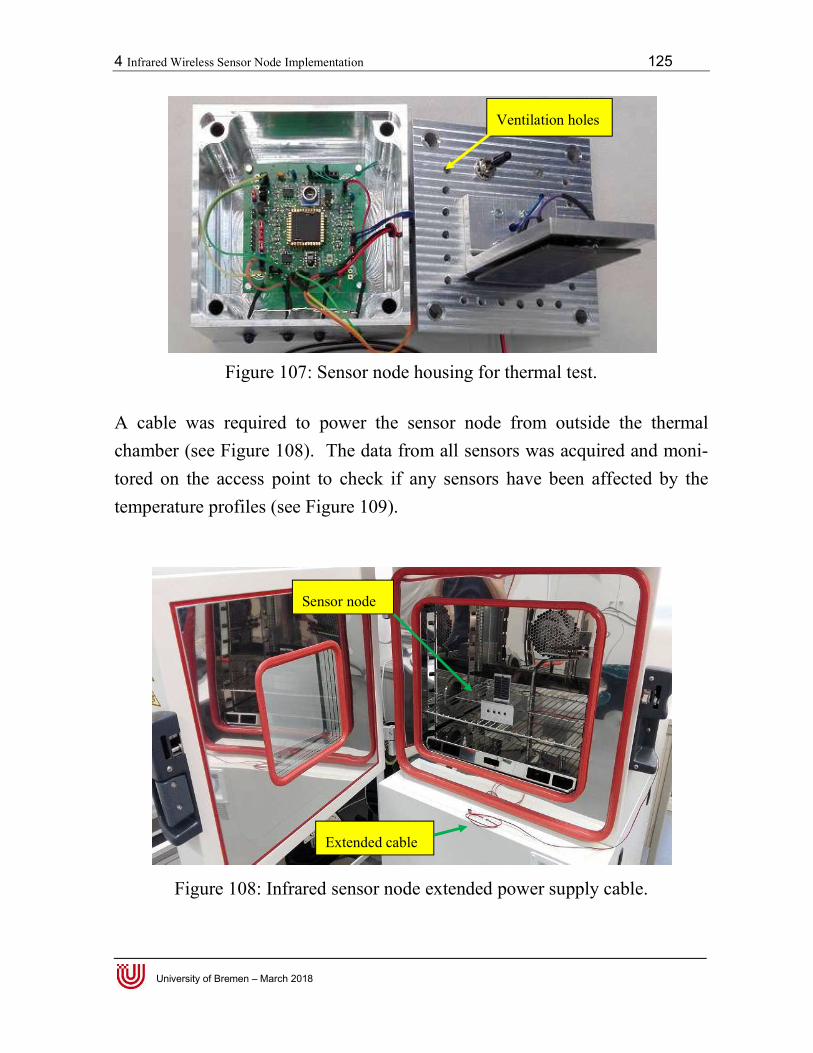
4 Infrared Wireless Sensor Node Implementation 125
University of Bremen – March 2018
Figure 107: Sensor node housing for thermal test.
A cable was required to power the sensor node from outside the thermal chamber (see Figure 108). The data from all sensors was acquired and moni-tored on the access point to check if any sensors have been affected by the temperature profiles (see Figure 109).
Figure 108: Infrared sensor node extended power supply cable.
Ventilation holes
Extended cable
Sensor node
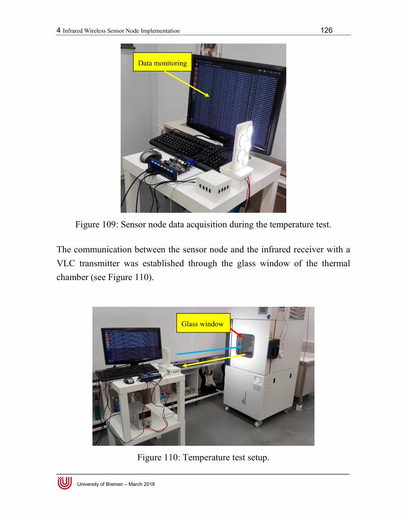
4 Infrared Wireless Sensor Node Implementation 126
University of Bremen – March 2018
Figure 109: Sensor node data acquisition during the temperature test.
The communication between the sensor node and the infrared receiver with a VLC transmitter was established through the glass window of the thermal chamber (see Figure 110).
Figure 110: Temperature test setup.
Data monitoring
Glass window
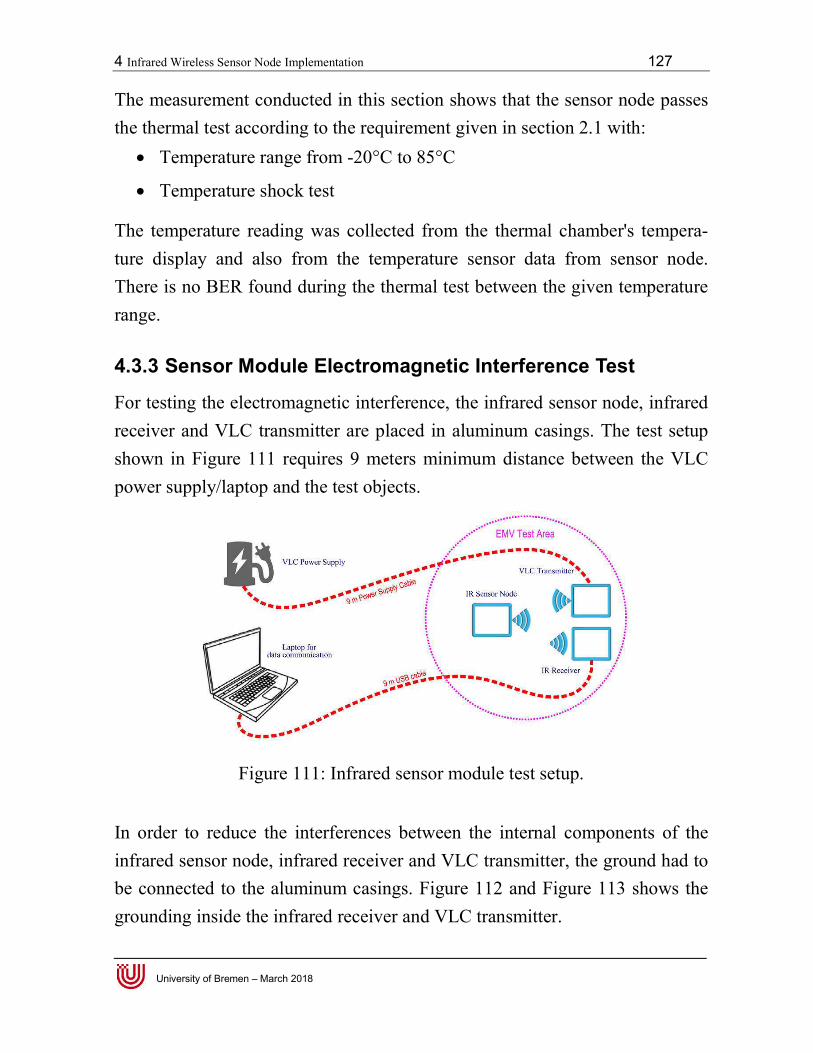
4 Infrared Wireless Sensor Node Implementation 127
University of Bremen – March 2018
The measurement conducted in this section shows that the sensor node passes the thermal test according to the requirement given in section 2.1 with: Temperature range from -20°C to 85°C
Temperature shock test
The temperature reading was collected from the thermal chamber's tempera-ture display and also from the temperature sensor data from sensor node. There is no BER found during the thermal test between the given temperature range.
4.3.3 Sensor Module Electromagnetic Interference Test
For testing the electromagnetic interference, the infrared sensor node, infrared receiver and VLC transmitter are placed in aluminum casings. The test setup shown in Figure 111 requires 9 meters minimum distance between the VLC power supply/laptop and the test objects.
Figure 111: Infrared sensor module test setup.
In order to reduce the interferences between the internal components of the infrared sensor node, infrared receiver and VLC transmitter, the ground had to be connected to the aluminum casings. Figure 112 and Figure 113 shows the grounding inside the infrared receiver and VLC transmitter.
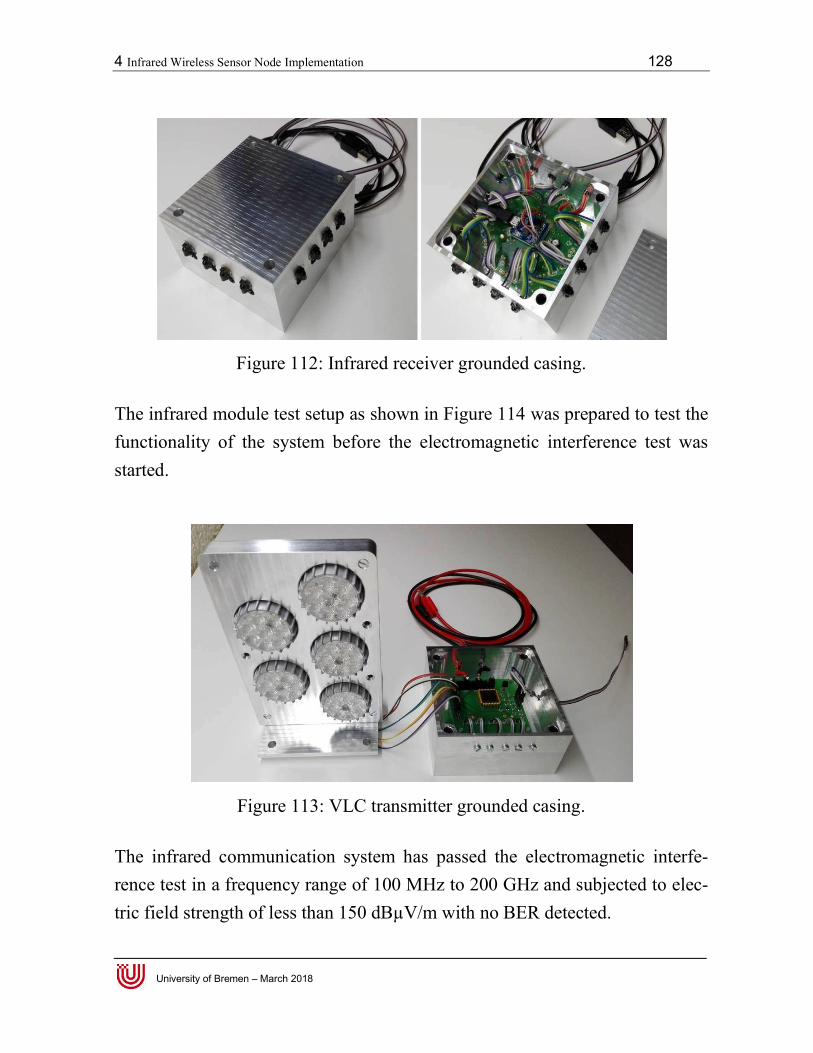
4 Infrared Wireless Sensor Node Implementation 128
University of Bremen – March 2018
Figure 112: Infrared receiver grounded casing.
The infrared module test setup as shown in Figure 114 was prepared to test the functionality of the system before the electromagnetic interference test was started.
Figure 113: VLC transmitter grounded casing.
The infrared communication system has passed the electromagnetic interfe-rence test in a frequency range of 100 MHz to 200 GHz and subjected to elec-tric field strength of less than 150 dBµV/m with no BER detected.
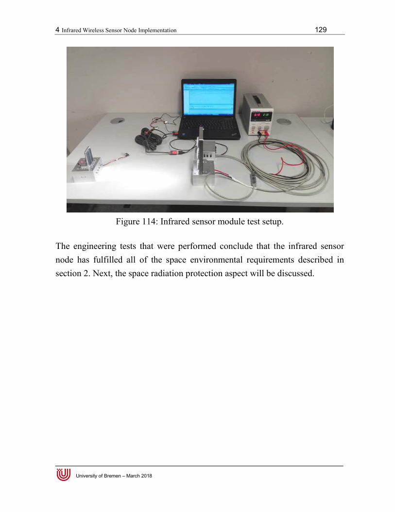
4 Infrared Wireless Sensor Node Implementation
University of Bremen – March 2018
Figure 114: Infrared sensor module test setup.
The engineering tests that were performed node has fulfilled all of the space environmental requirements described in section 2. Next, the space radiation protection aspect will be discussed.
Wireless Sensor Node Implementation
: Infrared sensor module test setup.
The engineering tests that were performed conclude that the infrared sensor filled all of the space environmental requirements described in
ace radiation protection aspect will be discussed.
129
that the infrared sensor filled all of the space environmental requirements described in
ace radiation protection aspect will be discussed.
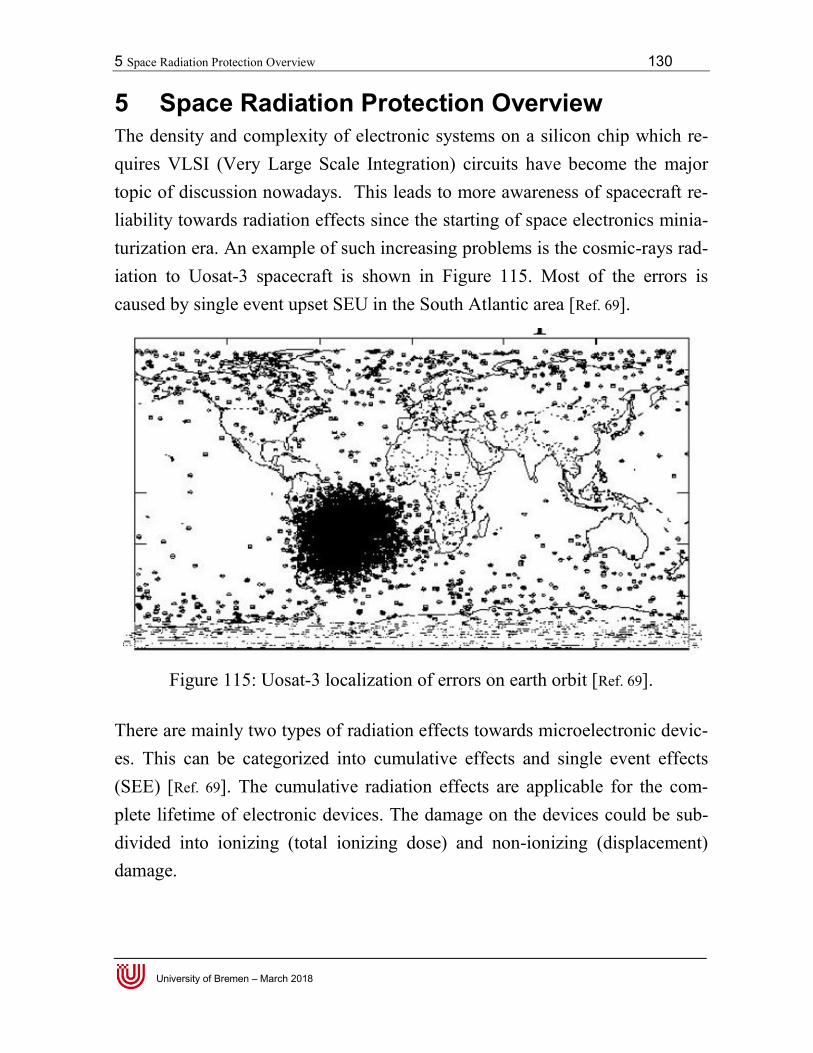
5 Space Radiation Protection Overview 130
University of Bremen – March 2018
5 Space Radiation Protection Overview The density and complexity of electronic systems on a silicon chip which re-quires VLSI (Very Large Scale Integration) circuits have become the major topic of discussion nowadays. This leads to more awareness of spacecraft re-liability towards radiation effects since the starting of space electronics minia-turization era. An example of such increasing problems is the cosmic-rays rad-iation to Uosat-3 spacecraft is shown in Figure 115. Most of the errors is caused by single event upset SEU in the South Atlantic area [Ref. 69].
Figure 115: Uosat-3 localization of errors on earth orbit [Ref. 69].
There are mainly two types of radiation effects towards microelectronic devic-es. This can be categorized into cumulative effects and single event effects (SEE) [Ref. 69]. The cumulative radiation effects are applicable for the com-plete lifetime of electronic devices. The damage on the devices could be sub-divided into ionizing (total ionizing dose) and non-ionizing (displacement) damage.

5 Space Radiation Protection Overview 131
University of Bremen – March 2018
All kinds of electronic components are subject to total ionizing dose (TID) ef-fects that are depending on the absorbed energy from the ions impacting the affected circuit. This absorption is independent of the type of radiation that is coming. The type of impacting particles, their energy level, the related shiel-ding efficiency, the particle sources and the orbits around the earth are sum-marized in Table 12.
Table 12: Type of impacting particles and their energy level [Ref. 70].
Solar flares Galactic cosmic rays Van Allen Belts Type of particles - Protons - Protons (85%) - Electrons (2 belts at
- Alpha particles (5-10%) - Alpha particles (14%) at 3000 and 20000 km)
- Heavy ions - Heavy ions (<1%) - Protons (1 belt at
- electrons 3000 km)
102…103 MeV per 400 MeV max for protons
Energy level Low nucleon 105 MeV for the most 7 MeV max for electrons
energetic
Exposed orbits High altitute orbits: - Polar orbits - Intermediary orbits
- Geosynchronous - High altitude orbits around 3000 km
- Far missions - Low orbits above
South Atlantic
The Single Event Effects (SEE) can be classified into non-destructive effects (so-called soft errors) and destructive effects producing damage (hard errors). The particle interaction with a MOS transistor that causes SEE is illustrated in Figure 116. The lists of non-destructive and destructive single event effects are described in Table 13 and Table 14 [Ref. 71]. There are mainly two methods used to increase the radiation tolerance of space electronics. The first is by selecting protective material that can absorb the energy of the particles and the second is by changing the transistor layout de-sign to be more radiation tolerant. Secondary solutions are software redundan-cy algorithm or circuit design redundancy techniques.

5 Space Radiation Protection Overview 132
University of Bremen – March 2018
Table 13: Non-destructive single event effects [Ref. 71].
Non-destructive effects
Type of effect Sensitive device Description
Single event registers, lat-ches change of the logic state of a latch or
upset (SEU) a memory cell
Single event combinational temporary deviation of an analog signal
transient (SET) logics, Opamps (analog equivalent of SEU)
Single event registers, lat-ches momentary corruption of the
disturb (SED) information stored in a bit
Table 14: Destructive single event effects [Ref. 71].
Destructive effects
Type of effect Sensitive device Description
Single event power transistors power devices are triggered in the OFF state
burnout (SEB) by a particle induced current transient. A par-
asitic or the main bipolar structure is turned
on and a positive feedback mechanism gner-
ates a destructive current by impac-ionisation
(avalanches).
Single event dielect-ric CMOS transistor heavi-ion-induced catastrophic failure of
failure (SEDF) DRAM or SRAM devices. Similar to the
SEGR phenomenon
Singel event Gate Power CMOS transistor A heavy-ion-induced localised dielectric break
rupture (SEGR) down of the gate oxide occuring in the tran-
sistor's OFF state (VGS < 0)
Single event latch-up CMOS transistor The triggering of a (parasitic) thyristor, typi-
(SEL) cally a combination of active and parasitic de-
vices, by a particle hit. The thyristor usually
operates between the power supplies and may
sustain destructive high currents.
Singel event CMOS transistor Switching a pn-junction to avalanche mode
snapback sustain a high current. Snapback does not in-
(SES) volve a positive feedback; imposes a maxi-
mum supply voltage constraint.
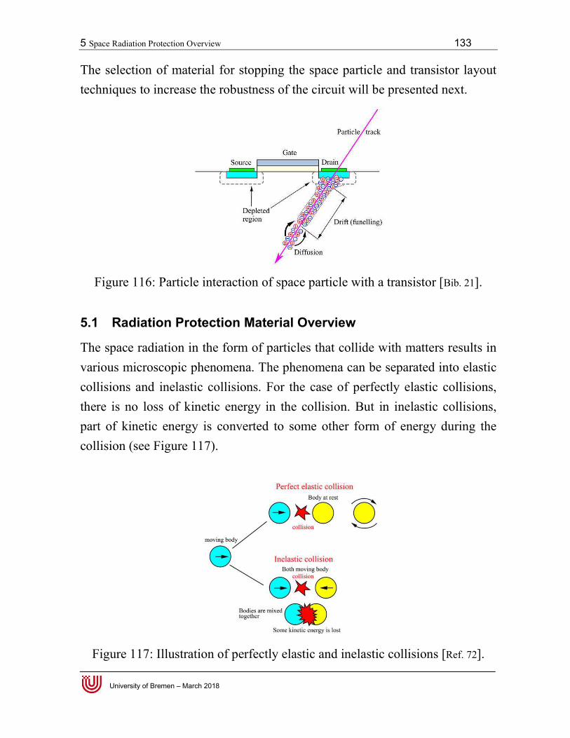
5 Space Radiation Protection Overview 133
University of Bremen – March 2018
The selection of material for stopping the space particle and transistor layout techniques to increase the robustness of the circuit will be presented next.
Figure 116: Particle interaction of space particle with a transistor [Bib. 21].
5.1 Radiation Protection Material Overview
The space radiation in the form of particles that collide with matters results in various microscopic phenomena. The phenomena can be separated into elastic collisions and inelastic collisions. For the case of perfectly elastic collisions, there is no loss of kinetic energy in the collision. But in inelastic collisions, part of kinetic energy is converted to some other form of energy during the collision (see Figure 117).
Figure 117: Illustration of perfectly elastic and inelastic collisions [Ref. 72].
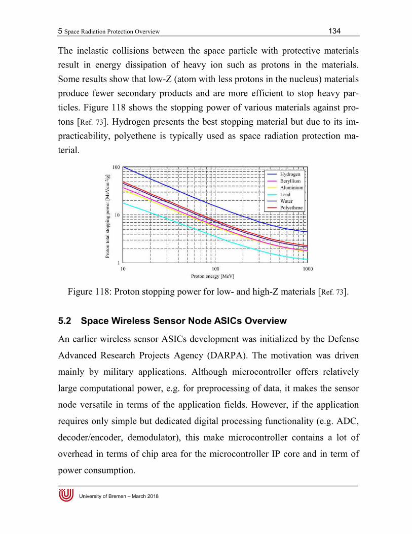
5 Space Radiation Protection Overview 134
University of Bremen – March 2018
The inelastic collisions between the space particle with protective materials result in energy dissipation of heavy ion such as protons in the materials. Some results show that low-Z (atom with less protons in the nucleus) materials produce fewer secondary products and are more efficient to stop heavy par-ticles. Figure 118 shows the stopping power of various materials against pro-tons [Ref. 73]. Hydrogen presents the best stopping material but due to its im-practicability, polyethene is typically used as space radiation protection ma-terial.
Figure 118: Proton stopping power for low- and high-Z materials [Ref. 73].
5.2 Space Wireless Sensor Node ASICs Overview
An earlier wireless sensor ASICs development was initialized by the Defense
Advanced Research Projects Agency (DARPA). The motivation was driven
mainly by military applications. Although microcontroller offers relatively
large computational power, e.g. for preprocessing of data, it makes the sensor
node versatile in terms of the application fields. However, if the application
requires only simple but dedicated digital processing functionality (e.g. ADC,
decoder/encoder, demodulator), this make microcontroller contains a lot of
overhead in terms of chip area for the microcontroller IP core and in term of
power consumption.

5 Space Radiation Protection Overview 135
University of Bremen – March 2018
In addition to that, this overhead is expensive for space applications because
all circuits must be radiation harden. An example of space wireless sensor
node based on ASIC with solar cell array, photo sensor and CCR receiver is
shown in Figure 119.
Figure 119: Optical wireless sensor node for space [Bib. 26].
In order to use the available ASICs process technologies effectively, the selec-tion of proper technologies shown in Table 15 is very important depending on the sensor node’s application.
Table 15: Some process technologies and their typical application [Ref. 82].
Technologies Specifications Common application BCD High voltage Actuators driving
High current driving Power stage driving
BiCMOS SiGe Low RF losses Gsps ADCs > 10 Gbit/s links Multi GHz RF
CMOS 250nm -130nm Standard analog circuit Standard Readout
Integrated Circuit
DSM 65nm - 22nm High Digital density FPGA, Processors, Mixed capabilities Telecom ASICs

5 Space Radiation Protection Overview 136
University of Bremen – March 2018
5.3 Radiation Layout Technique Overview Radiation hardened ASIC’s libraries for developing customized ASIC are normally very expensive. The libraries are typically not open because they are protected by intellectual properties (IP). This makes them very difficult for the scientific community to do transistor layout improvement for space ASIC de-sign. The well known radiation harden ASIC libraries are:
IMEC Design Against Radiation Effects (DARE) library [Ref. 74].
These libraries are provided by IMEC Belgium based research institute.
CERN 0.25 µm radiation hardened library [Ref. 75].
The libraries are provided by European Organization for Nuclear Re-
search (CERN) for particles accelerator in Switzerland.
BAE 0.15 µm radiation hardened library [Ref. 76].The libraries are de-
veloped and provided by BAE Systems PLC.
Ramon Chips 0.18 µm and 0.13 µm radiation hardened libraries [Ref.
77].The libraries are provided by Israel based company RAMON
CHIPS Ltd.
Cobham (former Aeroflex) 600, 250, 130 and 90 nm radiation hard-
ened libraries [Ref. 78].Cobham Semiconductor Solution in USA is pro-
viding various sizes of radiation hardened technologies libraries.
ST Microelectronics C65SPACE 65 nm radiation hardened library
[Ref. 79].These libraries are supplied by a French-Italian electronics
manufacturer STMicroelectronics.
Microchip MH1RT 0.35 µm and ATC18RHA 0.18 µm CMOS an-
dATMX150RHA 0.15 µm SOI CMOS radiation hardened libraries [Ref.
80].The libraries are provided by American based company ATMEL
Corporation.
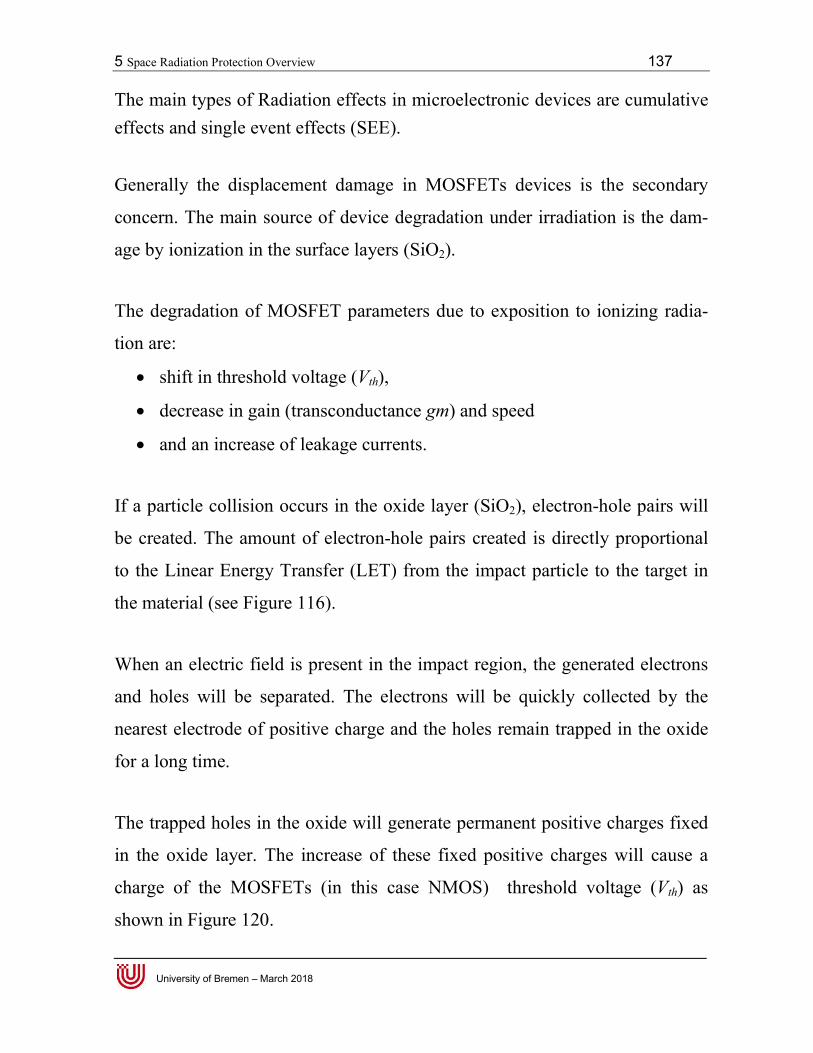
5 Space Radiation Protection Overview 137
University of Bremen – March 2018
The main types of Radiation effects in microelectronic devices are cumulative effects and single event effects (SEE).
Generally the displacement damage in MOSFETs devices is the secondary
concern. The main source of device degradation under irradiation is the dam-
age by ionization in the surface layers (SiO2).
The degradation of MOSFET parameters due to exposition to ionizing radia-
tion are:
shift in threshold voltage (Vth),
decrease in gain (transconductance gm) and speed
and an increase of leakage currents.
If a particle collision occurs in the oxide layer (SiO2), electron-hole pairs will
be created. The amount of electron-hole pairs created is directly proportional
to the Linear Energy Transfer (LET) from the impact particle to the target in
the material (see Figure 116).
When an electric field is present in the impact region, the generated electrons
and holes will be separated. The electrons will be quickly collected by the
nearest electrode of positive charge and the holes remain trapped in the oxide
for a long time.
The trapped holes in the oxide will generate permanent positive charges fixed
in the oxide layer. The increase of these fixed positive charges will cause a
charge of the MOSFETs (in this case NMOS) threshold voltage (Vth) as
shown in Figure 120.
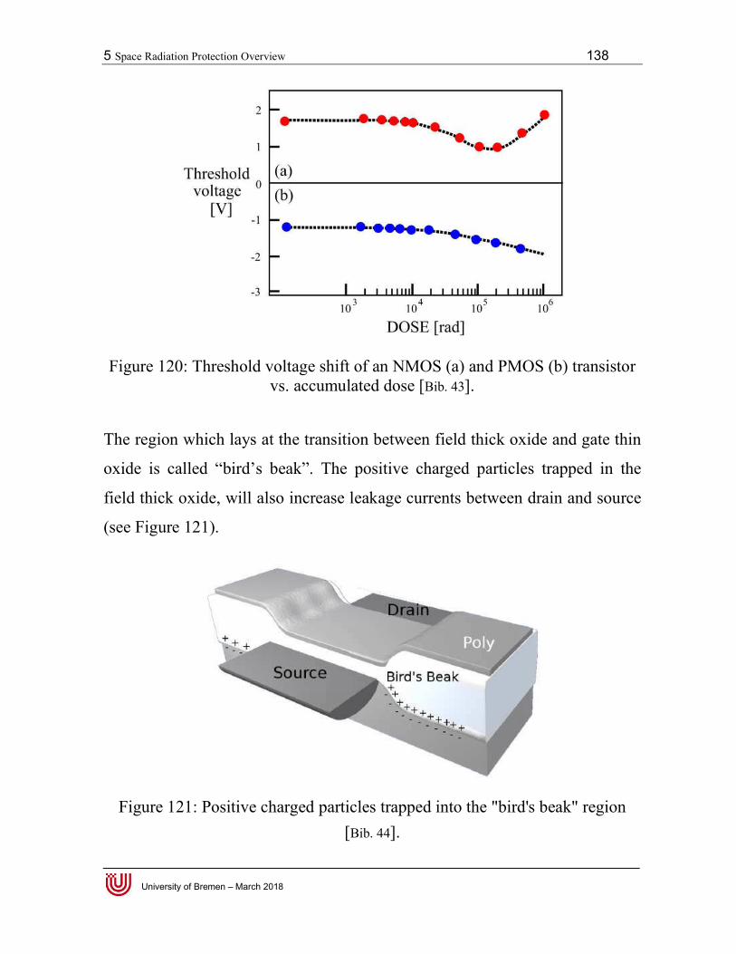
5 Space Radiation Protection Overview 138
University of Bremen – March 2018
Figure 120: Threshold voltage shift of an NMOS (a) and PMOS (b) transistor vs. accumulated dose [Bib. 43].
The region which lays at the transition between field thick oxide and gate thin
oxide is called “bird’s beak”. The positive charged particles trapped in the
field thick oxide, will also increase leakage currents between drain and source
(see Figure 121).
Figure 121: Positive charged particles trapped into the "bird's beak" region [Bib. 44].
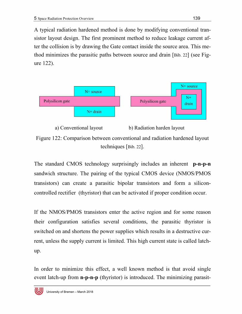
5 Space Radiation Protection Overview 139
University of Bremen – March 2018
A typical radiation hardened method is done by modifying conventional tran-sistor layout design. The first prominent method to reduce leakage current af-ter the collision is by drawing the Gate contact inside the source area. This me-thod minimizes the parasitic paths between source and drain [Bib. 22] (see Fig-ure 122).
a) Conventional layout b) Radiation harden layout
Figure 122: Comparison between conventional and radiation hardened layout techniques [Bib. 22].
The standard CMOS technology surprisingly includes an inherent p-n-p-n
sandwich structure. The pairing of the typical CMOS device (NMOS/PMOS
transistors) can create a parasitic bipolar transistors and form a silicon-
controlled rectifier (thyristor) that can be activated if proper condition occur.
If the NMOS/PMOS transistors enter the active region and for some reason
their configuration satisfies several conditions, the parasitic thyristor is
switched on and shortens the power supplies which results in a destructive cur-
rent, unless the supply current is limited. This high current state is called latch-
up.
In order to minimize this effect, a well known method is that avoid single event latch-up from n-p-n-p (thyristor) is introduced. The minimizing parasit-
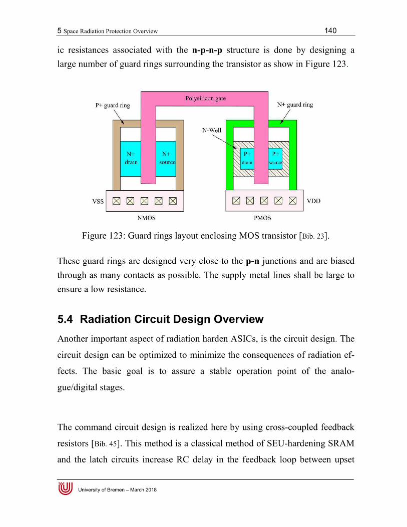
5 Space Radiation Protection Overview 140
University of Bremen – March 2018
ic resistances associated with the n-p-n-p structure is done by designing a large number of guard rings surrounding the transistor as show in Figure 123.
Figure 123: Guard rings layout enclosing MOS transistor [Bib. 23].
These guard rings are designed very close to the p-n junctions and are biased through as many contacts as possible. The supply metal lines shall be large to ensure a low resistance.
5.4 Radiation Circuit Design Overview Another important aspect of radiation harden ASICs, is the circuit design. The
circuit design can be optimized to minimize the consequences of radiation ef-
fects. The basic goal is to assure a stable operation point of the analo-
gue/digital stages.
The command circuit design is realized here by using cross-coupled feedback
resistors [Bib. 45]. This method is a classical method of SEU-hardening SRAM
and the latch circuits increase RC delay in the feedback loop between upset
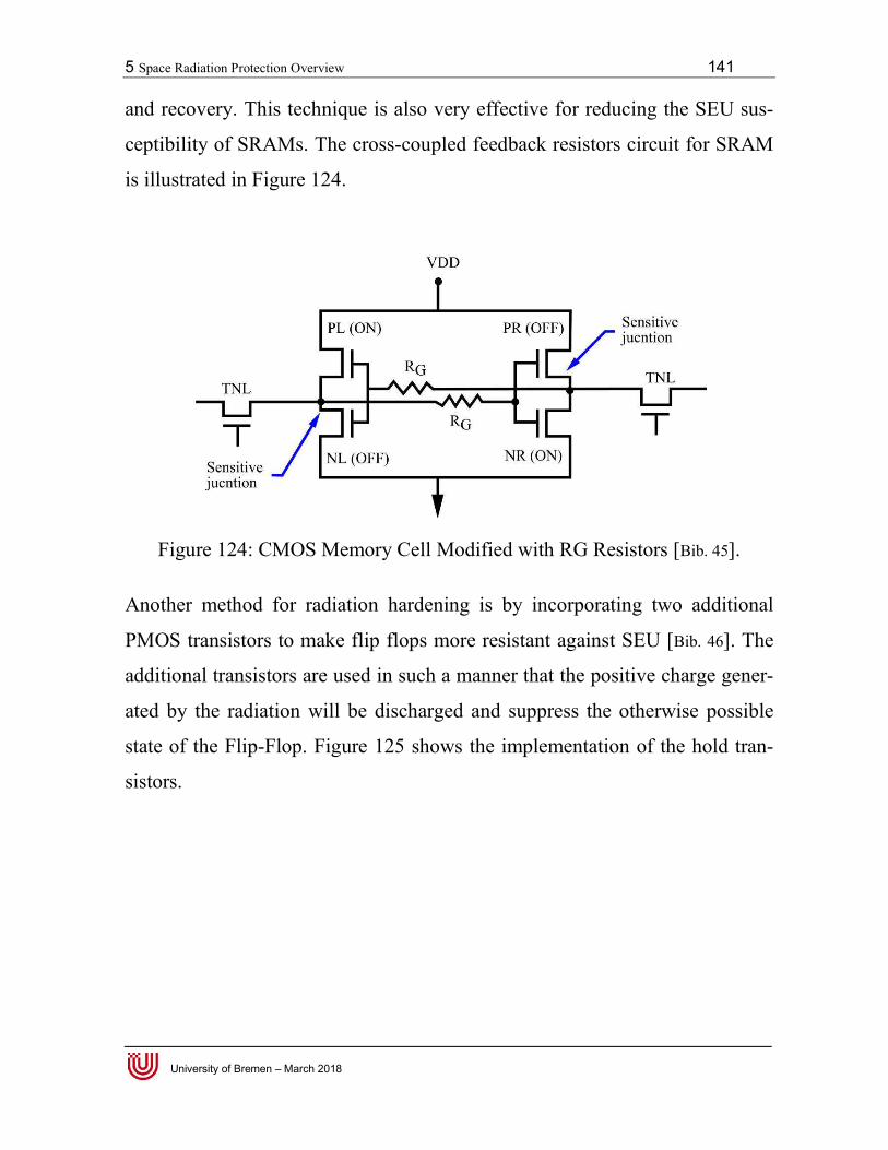
5 Space Radiation Protection Overview 141
University of Bremen – March 2018
and recovery. This technique is also very effective for reducing the SEU sus-
ceptibility of SRAMs. The cross-coupled feedback resistors circuit for SRAM
is illustrated in Figure 124.
Figure 124: CMOS Memory Cell Modified with RG Resistors [Bib. 45].
Another method for radiation hardening is by incorporating two additional
PMOS transistors to make flip flops more resistant against SEU [Bib. 46]. The
additional transistors are used in such a manner that the positive charge gener-
ated by the radiation will be discharged and suppress the otherwise possible
state of the Flip-Flop. Figure 125 shows the implementation of the hold tran-
sistors.

5 Space Radiation Protection Overview 142
University of Bremen – March 2018
Figure 125: Schematic of a flip flop with two additional PMOS hold transis-tors [Bib. 46].
In this section, the radiation effects, radiation harden by design layout and cir-cuit techniques have been introduced. There are many radiation hardened li-braries have been identified such as UMC180 or MH1RT 0.35 µm, which may be used for further development to build infrared transceivr ASIC against space radiation.
Furthermore, the ASIC the infrared transceiver with AMS35nm technologies
describes in the previous section is not typically for radiation hardened ASIC
development, but some consideration has been taken for radiation hardened
concept. This can be seen from the development of the pulse 3/16 pulse shap-
ing that replace digital circuit with analog circuit that uses single transistor to
invert the input signal. This circuit reduces forming parasitic thyristor effect
compare to typical digital cell that uses PMOS/NMOS pair to build inverter,
when single event latch-up occurs. The summary and discussion of all sec-
tions from this work will be concluded next.
6 Summary and Discussion 143
University of Bremen – March 2018
6 Summary and Discussion The steps taken to develop a low power design of a versatile analog mixed signal sensor module have been presented in this dissertation. The steps and their results are presented as following:
Step 1: General space requirement overview as described in section 2
provides information about the Ariane 5's requirements. The environ-
ment requirements such as mechanical, pressure, thermal and electro-
magnetic interference were used to design a sensor module prototype
that is suitable for European launcher. The first implication of the re-
quirements to the design is the selection of infrared and visible light
communication system which minimizes the electromagnetic interfer-
ence to the on board equipment in the VEB. The second implication of
the requirements is to design the infrared transceiver ASIC that allows
transition for future design with the commercial radiation hardened li-
braries in the market.
Step 2: The selection of commercial wireless communication systems
and energy harvesting methods as described in section 4 have been
made to increase sensor module lifetime during the mission. In order to
fulfil the electromagnetic interference requirements presented in section
2, a comparison was made between the existing wireless technologies
and this work. Although there are many available energy harvesting
products on the market, wireless energy transfer by using visible light
communication that powers solar cell as well as providing data trans-
mission has been proven to be the optimum solution to be used inside a
VEB.
Step 3: Some qualified space sensors and smart sensors have been pre-
sented in section 5. Although the smart sensors could not fully replace
6 Summary and Discussion 144
University of Bremen – March 2018
the space qualified sensors but they offer less energy consumption and
small in size if they are used together with wireless sensor nodes. The
miniaturization of sensor node makes them advantageous especially for
some places inside VEB that could not be easily equipped with space
qualified sensors.
Step 4: The characteristic of space material that is mostly covering the
spacecraft surface were studied in section 6. The investigation of MLI
effects on the infrared communication has shown promising results es-
pecially when the visible light from LED is used for energy transfer in a
confined room.
Step 5: The infrared transceiver ASIC design was done according to the
IrDA physical layer standard and was described in section 7. There are
two modulation methods that are realized on the ASICS. Both of them
show very low power consumption (less than 800 µW). The uni-polar
non return to zero modulation shows more promising results due to its
simplicity in the ASIC design.
Step 6: The implementation of the infrared ASIC on a wireless sensor
node is described in section 8 and shows various technologies as de-
scribed Table 8. Some capabilities for the sensor node are listed below:
- Energy harvesting capability (max. 3.5 mW)
- Visible light communication capability (max. 300 cm)
- Various digital interface capability to smart sensors
- Analog signal acquisition capability (with 10 bit ADC)
- Infrared communication capability (9600 baud at 3 m)
- Time stamping capability (accuracy ± 3µs)
6 Summary and Discussion 145
University of Bremen – March 2018
The infrared subsystem was fully functional and performed as expected
in the presence of MLI. The light distribution in the VEB and the com-
munication range of the sensor nodes were measured and the results
show that with 2.8 W visible light power, it able to provide commands
and energy that activate the sensor nodes in a distance of more than 200
cm with 77 lux light intensity.
Step 7: In order to fulfil the Arine 5 requirements as described in sec-
tion 2, engineering tests were carried out and the results have been pre-
sented in section 9. Aluminium casings were built for the sensor nodes,
infrared receivers and VLC transmitter. These casings were used for
protection during the engineering tests. The tests have been performed
with the following results:
- In the mechanical tests, the sensor node passed the mechanical
test and survived sinusoidal vibration at 0.8 g at 100 Hz in
longitudinal and lateral direction. It also survived shock test at:
- 650 g at 400 Hz
- 880 g at 665 Hz
- 2000 g at 1000 Hz up to 20000 g at 10000 Hz
- In the thermal test, the sensor node worked within the given
temperature range of -20°C to 85°C.
- In the electromagnetic interference test, the infrared subsystem
passed the electromagnetic interference tests within a frequency
range of 100 MHz to 200 GHz and subjected to electric field
strength of less than 150 dBµV/m.
Step 8: The space radiation protections were presented in section 10.
There are many radiation harden libraries that can be used to manufac-
tured an infrared transceiver ASIC with space radiation tolerant but they

6 Summary and Discussion 146
University of Bremen – March 2018
are mostly very costly and are protected by intellectual properties. An
alternative solution is to design the radiation hardened infrared trans-
ceiver ASIC with the current AMS350 nm technology enhanced by
space radiation hardened layout techniques.
All of the steps mentioned above conclude the work for developing a low power versatile analog mixed signal sensor module that fulfils the environ-mental requirements for Ariane 5’s VEB.
7 Bibliography 147
University of Bremen – March 2018
7 Bibliography
[Bib. 2] Hewlett-packard Company, "The IrDA Standards for High-Speed Infrared Communi-cation", The Hewlett-Packard Journal, 1998.
[Bib. 1] Intel Architecture Labs, Intel Corp, "Ultra-Wideband Technology for Short- or Me-dium-Range Wireless Communications", Intel Technology Journal Q2, 2001.
[Bib. 3] B. HU, X. YU, L. HE, W. M. LIM, K. S. Yeo, "Analysis and Design of Wideband Low Noise Amplifier with Digital Control", Radioengineering, Vol. 19, No. 4, 2010.
[Bib. 4] I. S. C. Lu, N. Weste, S. Parameswaran,"ADC Precision Requirement for Digital Ultra-Wideband Receivers with Sublinear Front-ends: a Power and Performance Perspec-tive", International Conference on VLSI Design (VLSID’06), 2016.
[Bib. 5] F. Ahmed, Y. L. Moullec, P. Annus, "Energy Harvesting Technologies - Potential ap-plication to Wearable Health-Monitoring", The 10th International Conference on Bio-electromagnetism, pp. 1-4, Tallin, 2015.
[Bib. 6] Joseph M. Kahn, and John R. Barry, "Wireless Infrared Communication," Proceedings of the IEEE, vol. 85, No. 2, pp. 265 - 298, February 1997.
[Bib. 7] Fritz R. Gfeller, and Urs Bapst, "Wireless In-House Data Communication via Diffuse Infrared Radiation," Proceedings of the IEEE, vol. 67, No. 11, pp. 1474- 1486, No-vember 1979.
[Bib. 8] S. M. Kim, J. S. Won, "Simultaneous reception of visible light communication and optical energy using a solar cell receiver ". ICT Convergence (ICTC), 2013. pp. 896 - 897, 2013
[Bib. 9] S. Gaddis, "NASA Space Technology Mission Directorate and Game Changing Devel-opment Program", AIAA Adaptive Structure Conference, 2013.
[Bib. 10] W. L. Johnson, D. J. Frank, T. C. Nast, J. E. Fesmire, "Thermal Performance Testing of Cryogenic Multilayer Insulation with Silk Net Spacers", IOP Conference, Vol. 101, 2015.
[Bib. 11] T. Miyakita, R. Hatakenaka, H. Guita, M. Saitoh, T. Hirai, "Evaluation of Thermal Insulation Performance of a New Multi-Layer Insulation with NonInterlayer-Contact Spacer", ICES conference, 2015.
[Bib. 12] J. Zhang, T. S. Fisher, "A Review of Heat Transfer Issues in Hydrogen Storage Tech-nologies", Journal of Heat transfer, 2005.
[Bib. 13] H. Park, J. R. Barry, "Modulation Analysis for Wireless Infrared Communications", IEEE International Conference on Communications, 1995.
7 Bibliography 148
University of Bremen – March 2018
[Bib. 14] D. H. Whalen, E. R. Wiley, P. E. Rubin, F. S. Cooper, "The Haskins Laboratories's Pulse Code Modulation (PCM) System", Haskins Laboratories Status Report on Speech Research, SR-103/104, pp. 125-136 1990.
[Bib. 15] L. W. Couch II, "Digital and Analog Communication Systems", 5th Edition, Prentice Hall, 1997.
[Bib. 16] M. Seyedzadegan, M. Othman, "IEEE 802.16: WiMAX Overview, WiMAX Architec-ture", International Journal of Computer Theory and Engineering, vol. 5, No. 5, 2013.
[Bib. 17] J. Saphira, S. Miller, "CDMA Radio with Repeaters", Springer, 2000.
[Bib. 18] M. Rahman, S. Manir, "Performance Analysis of Sc-FDMA and OFDMA in LTE Frame Structure", International Journal of Computer Application, Vol. 45, No. 23, 2012.
[Bib. 19] R. Sun, J. Guo, E. K. A. Gill, "Opportunities and Challenges of Wireless Sensor Net-work in Space", International Astronautical Congress, 2010
[Bib. 20] H. J. Besstermueller, J. Sebald, H.-J. Borchers, M. Schneider, H. Luttmann, V.Schmid,‘Wireless-Sensor Networks in Space Technology Demonstration on ISS’, Dresdner Sensor-Symposium 2015.
[Bib. 21] F. Anghinolfi, "Radiation Hard Electronics". CERN/EP, pp. 1-54., 2000.
[Bib. 22] W. Jing, X. Zuocheng, H. Ping, W. Tianran, F. Guitao,"Practice on Layout-Level Radi-ation Hardened Technologies for I/O cells" International Conference on Information, Networking and Automation, Vol. 1, pp. 365- 369, 2010.
[Bib. 23] L. Lingjuan, L. Ruping, L. Min, S. Zehua, Z. Shichang, Y. Genqing, "Performance comparison of radiatio-hardened layout techniques", Journal of Semiconductor, Vol.35, pp. 1-6 ,2014.
[Bib. 24] Barnhart, David J., " Design of self-powered wireless system-on-a-chip sensor nodes
for hostile environments," Circuits and Systems, p. 824 - 827, 2008.
[Bib. 25] Christian C., " WiseNET: an ultralow-power wireless sensor network solution,"
Computer, Journals & Magazines, p. 62 – 70, 2004.
[Bib. 26] Warneke, Brett A., " An autonomous 16 mm3 solar-powered node for
distributed wireless sensor networks," IEEE Sensors Proceedings, p. 1510 – 1515,
vol. 2, 2002.
[Bib. 27] K. Romer and F. Mattern., " The design space of wireless sensor network,"
IEEE Wireless Communications, p. 54 – 61, vol. 11, no. 6, Dec. 2004.
7 Bibliography 149
University of Bremen – March 2018
[Bib. 28] E. Sanchis, E. Maset, A. Ferreres, J. Ejea, "High-Power Battery Discharge Regulator for Space Applications", IEEE Journals & Magazines, v. 57, issue 12, pp. 3935 - 3943, 2010.
[Bib. 29] C. Pearson, K. Schrantz, J. Neubauer, "Lithium-ion space battery technology develop-ment and infusion", 2010 IEEE Aerospace Conference, pp. 1 -12, 2010.
[Bib. 30] M. Mangrulkar, S. Akojwar, "A simple and efficient solar energy harvesting for wire-less sensor node", IEEE International Conference on Research in Computational Intel-ligence and Communication Networks, pp. 95 -99, 2016.
[Bib. 31] A. Mouapi, N. Hakem, "Performance evaluation of wireless sensor node powered by RF energy harvesting", IEEE Mediterranean Microwave Symposium, pp. 1-4, 2016.
[Bib. 32] L. Perisoara, R. Stoian, L. Sucu, "Wireless sensor node for fruit growing monitoring", IEEE International Symposium for Design and Technology in Electronic Packaging, 2016.
[Bib. 33] Z. Ghassemlooy, W. O. Popoola, S. Rajbhandari, M. Amiri, S. Hashemi, "A synopsis of modulation techniques for wireless infrared communication", IEEE ICTON Mediter-ranean Winter Conference, pp. 1 - 6, 2007.
[Bib. 34] A. Takacs, H. Aubert, M. Bafleur, J. M. Dilhac, F. Courtade, S. Fredon, L. Despoisse, C. Vanhecke, G. Cluzet, "Energy Harvesting for Powering Wireless Sensor Networks On-Board Geostationary Broadcasting Satellites", IEEE International Conference on Green Computing and Communications, pp. 637 - 640, 2012.
[Bib. 35] M. Perelli, A. Negri, M. Marino, "Miniaturized bio-sensor for environment monitoring in manned space mission", IEEE 15th International Conference on Nanotechnology, pp 881 - 884, 2015.
[Bib. 36] F. Patlar, A. Zaim, G. Yilmaz, "Wireless sensor networks for space and Solar-system missions", 5th International Conference on Recent Advances in Space Technologies, pp. 616 - 618, 2011.
[Bib. 37] T. Vladimirova, X. Wu, C. Bridges, "Development of a Satellite Sensor Network for Future Space Missions", IEEE Aerospace Conference, pp. 1 - 10, 2008.
[Bib. 38] J. Elson, L. Girod, and D. Estrin, “Fine-grained network time synchronization using reference broadcasts,” SIGOPS Oper. Syst. Rev., vol. 36, no. SI, pp. 147–163, Dec. 2002.
[Bib. 39] S. Ganeriwal, R. Kumar, and M. B. Srivastava, “Timing-sync protocol for sensor net-works,” in Proceedings of the 1st International Conference on Embedded Networked Sensor Systems, ser. SenSys ’03. New York, NY, USA: ACM, 2003, pp. 138–149.
[Bib. 40] P. Sommer and R. Wattenhofer, “Gradient clock synchronization in wireless sensor networks,” in Information Processing in Sensor Networks, 2009. IPSN 2009. Interna-tional Conference on, April 2009, pp. 37–48.
[Bib. 41] A. Tahmasi; H. Hematkhah; Y. S. Kavian, "Visible light communication based optical link for data transmission in Wireless Sensor Networks", IEEE 10th International Sym-posium on Communication Systems, Networks and Digital Signal Processing (CSNDSP)pp. 1 - 6, 2016.
[Bib. 42] D. Krichen; W. Abdallah; N. Boudriga,"An optical wireless network for railways con-dition monitoring", IEEE 22nd Asia-Pacific Conference on Communications (APCC), pp. 153 - 160, 2016.
7 Bibliography 150
University of Bremen – March 2018
[Bib. 43] Daniel Baumeister, "Development and Characterisation of a Radiation Hard
Readout Chip for the LHCb-Experiment". Ruperto-Carola University of
Heidelberg 2003. p. 1 - 196.
[Bib. 44] A. Stabile, V. Liberali, C. Calligaro, "Design of a Rad-Hard Library of Digital
Cells for Space Applications". IEEE ICECS, p. 1 – 4, 2008.
[Bib. 45] J. L. Andrews, J. E. Schroeder, B. L. Gingerich, W. A. Kolasinski, R. Koga,
and S. E. Diehl, " Single event error immune CMOS RAM". IEEE Nuclear
Science, p. 2040 – 2043, 1982.
[Bib. 46] U. Jagdhold, "Creation of a Radiation Hard 0.30 Micron CMOS Library at
IHP". VDE-Verlag, p. 1 – 196, 2012.
[Bib. 47] P. Welch, “The use of fast Fourier transform for the estimation of power spectra: A method based on time averaging over short, modified periodograms”, IEEE Transac-tions on Audio and Electroacoustics,Vol.15, pp.70 - 73 , 1967.
[Bib. 48] S. Zhao, J. Xu, and O. Trescases, “A dimmable led driver for visible light communica-tion (vlc) based on llc resonant dc-dc converter operating in burst mode,” in 28th
Annual IEEE Applied Power Electronics Conference and Exposition (APEC), Long
Beach, California, USA, pp. 2144–2150, 2013.
[Bib. 49] H. Ma, L. Lampe, and S. Hranilovic, “Integration of indoor visible light and power
line communication systems,” in 17th IEEE International Symposium on Power Line
Communications and its Applications (ISPLC), Johannesburg, South Africa, pp.
291–296, 2013.
[Bib. 50] D. Steigerwald, J. Bhat, D. Collins, R. Fletcher, M. Holcomb, M. Ludowise, P. Martin, and S. Rudaz, “Illumination with solid state lighting technology,” IEEE Journal of Selected Topics in Quantum Electronics, vol. 8, no. 2, pp. 310–320, 2002.
[Bib. 51] H. Le Minh, Z. Ghassemlooy, A. Burton, and P. A. Haigh, “Equalization for organic light emitting diodes in visible light communications,” in IEEE GLOBECOM Work-shops (GC Wkshps), Houston, Texas, pp. 828–832, USA, 2011.
[Bib. 52] Z. Ghassemlooy, “Oled-based visible light communications,” in IEEE Photonics Socie-ty Summer Topical Meeting Series, Seattle, Washington, USA, pp. 102–104, 2012.
[Bib. 53] P. A. Haigh, Z. Ghassemlooy, M. Hoa Le, S. Rajbhandari, F. Arca, S. F. Tedde, O. Hayden, and I. Papakonstantinou, “Exploiting equalization techniques for improving data rates in organic optoelectronic devices for visible light communications,” Journal of Lightwave Technology, vol. 30, no. 19, pp. 3081–3088, 2012.
[Bib. 54] H. Chun, C.-J. Chiang, and D. C. O’Brien, “Visible light communication using oleds: Illumination and channel modeling,” in International Workshop on Optical Wireless Communications (IWOW), Pisa, Italy, pp. 1–3, 2012.
[Bib. 55] H. Jiang and J. Y. Lin, “Nitride micro-leds and beyond - a decade progress review,” Opt. Express, vol. 21, no. S3, pp. A475–A484, 2013.
7 Bibliography 151
University of Bremen – March 2018
[Bib. 56] Prasad, R, Mihovska, A. ; Cianca, E. ; Mukherjee, S., "Comparative overview of UWB and VLC for data-intensive and security-sensitive applications". IEEE International Conference on Ultra-Wideband (ICUWB), pp. 41 - 45, 17-20 Sept. 2012.
[Bib. 57] J. M. Kahn, W. J. Krause, and J. B. Carruthers, “Experimental characterization of non-directed indoor infrared channels,” IEEE Trans. Commun., vol. 43, pp. 1613–1623, 1995.
[Bib. 58] "IEEE 802.15 WPAN Task Group 7 (TG7) Visible Light Communication". IEEE Stan-dards Association. April 9, 2011.
[Bib. 59] J. Le, C. Hanken, M. Held, M. Hagedorm, K. Mayaram, and T. Fiez, “Comparison and impact of substrate noise generated by clocked and clockless digital circuitry,” in Cus-tom Integrated Circuits Conference, 2006. CICC’06. IEEE. IEEE, pp. 105–108, 2006.
[Bib. 60] S. Furber, Principles of asynchronous circuit design: a systems perspective. Springer Netherlands, 2001.
[Bib. 61] J. Le, C. Hanken, M. Held, M. Hagedorm, K. Mayaram, and T. Fiez, “Comparison and impact of substrate noise generated by clocked and clockless digital circuitry,” in Cus-tom Integrated Circuits Conference, 2006. CICC’06. IEEE. IEEE, pp. 105–108, 2006.
[Bib. 62] C. Hanken, J. Le, T. Fiez, and K. Mayaram, “Simulation and modeling of substrate noise generation from synchronous and asynchronous digital logic circuits,” CICC’07. IEEE. Custom Integrated Circuits Conference, pp. 845–848, 2007.
[Bib. 63] C. Monteleone, “Microcontrollers for Embedded Space Applications”, ESA/ESTEC ,
MESA conference 2010.
[Bib. 64] A. Heinig "Optical wireless data transmission with a sensor network integrated in atextile-reinforced composite", IEEE Sensors Proceedings, p 1- 5, 2010.
[Bib. 65] D. Bol, J. De Vos, C. Hocquet, F. Botman, F. Durvaux, S. Boyd, " SleepWalk er: A 25-MHz 0.4-V Sub- mm2 7- µW/MHz Microcontroller in 65-nm LP/GP CMOS for Low-Carbon Wireless Sensor Nodes", IEEE Solid-State Circuits, p. 1 – 13, 2013.
[Bib. 65] A. D. Molnar, "An Ultra-Low Power 900MHz RF Transceiver for Wireless Sensor Networks" IEEE Custom Integrated Circuits, p. 1 – 4, 2004.
[Bib. 66] Bol, D., De Vos, J.; Hocquet, C.; Botman, F.; Durvaux, F.; Boyd, S.," SleepWalker: A 25-MHz 0.4-V Sub- mm2 7- µW/MHz Microcontroller in 65-nm LP/GP CMOS for Low-Carbon Wireless Sensor Nodes", IEEE Solid-State Circuits, p. 1 – 13, 2013.
8 References 152
University of Bremen – March 2018
8 References [Ref. 1] ECSS Secretariat ESA-ESTEC Requirements & Standards Division Noordwijk, "The
European Cooperation for Space Standardization ECSS", The Netherlands, 2016. [Ref. 2 ] European Space Agency, "Space Engineering and Technology, About Future
launchers Praparatory Programme (FLPP)", ESA Communication Department ESRIN, Italy 2016.
[Ref. 3] Arianespace launch Service & Solution company, "Ariane 5 User's manual", issue 5 revision 1 July 2011.
[Ref. 4] “The VEB for Ariane 5G’s third and Last Qualification Flight” ESA/CNES/ Arianes-
pace, Id209081, 2004. [Ref. 5] Airbus Defence & Space S.A.S, "ATV-2, Johannes Kepler", January 2011. [Ref. 6] Ariane 5 Attitude Control System", Airbus Defense & Space, 2015. [Ref. 7] Decawave, "ScenSor DWM1000 Module", Decawave Ltd, 2015. [Ref. 8] Decawave, "ScenSor DWM1000 Module Product Overview", Decawave Ltd, 2015. [Ref. 9] "IR Sensor Module for Remote Control Systems, TSMP58000", Vishay corp. Rev. 1.2,
pp. 1-5, May 2014. [Ref. 10] "High Power Infrared Emitting Diode, 940 nm, GaAIAs, MQW, TSAL6200", Vishay
corp. Rev. 2.4, pp. 1-5, March 2014. [Ref. 11] B. S. Randhawa, "Conducted and Radiated Measurements for Low Level UWB Emis-
sions", ERA technology Ltd., 2007. [Ref. 12] M. Raju, "ULP meets energy harvesting, A game-changing combination for design
engineers", Texas Instruments Incorporated, 2008. [Ref. 13] "P2110-EVAL-01 Lifetime Power® Energy Harvesting Development Kit for Wireless
Sensors", Powercast Corporation, 2015. [Ref. 14] "P2110B 915 MHz RF Powerharvester® Receiver", Powercast Corporation, Rev. A,
2015 [Ref. 15] "ThermoHarvesting Module", EH4 GmbH, 2016. [Ref. 16] "TE-CORE ThermoHarvesting Power Module", Micropelt - preliminary - Datasheet
TE-CORE6 v3.1, 2015. [Ref. 17] "Midé’s piezo standard Piezo Protection Advantage (PPA) datasheet", MIDE Technol-
ogy Corp, Rev. Mo. 002, 2016. [Ref. 18] "Vibration Energy Harvesting with Piezoelectrics", MIDE Technology Corp, 2016.

8 References 153
University of Bremen – March 2018
[Ref. 19] "LTC3331 UPS System for Wireless Mesh Networks with Output Supercapacitor
Energy Storage", Linear Technology Corporation, 2014. [Ref. 20] "Energy Harvesting: Solar", Texas Instruments Incorporated, Rev. SLYY027, 2011. [Ref. 21] "Smart Sustainable Solar", G24 Power Limited, United Kingdom, 2016. [Ref. 22] "World’s first indoor solar powered iBeacon", G24 Power Limited, United Kingdom,
2016. [Ref. 23] "Solar Energy Harvesting", Linear Technology Corporation, 2014. [Ref. 24] "Solar Cell Technology - Latest Energy Efficiency News", Clixoo Solutions Private
Limited, 2016. [Ref. 25] C. Knutson, J. Brown, "IrDA Principles and Protocols", Infrared Data Association,
2011. [Ref. 26] Bonnie C. Baker, “Wireless Communication Using the IrDA Standard Protocol”, Mi-
crochip Technology, Inc., pp. 1-2, 2003 [Ref. 27] "Technical node: RF remote control as a replacement for IR remote control", Nordic
semiconductor, 2008. [Ref. 28] "TSSP77038, IR Receiver Modules for Remote Control Systems", Vishay Semicon-
ductors, Rev. 1.5, 2016. [Ref. 29] "Introduction of visible light communication", Visible Light Communications Consor-
tium, 2007. [Ref. 30] "Li-Fi is 100 times faster than WLAN", yeebase media, 2015. [Ref. 31] "About LiFi", pureLiFi Ltd, 2014. [Ref. 32] "Esterline Advance Sensors" Weston Aerospace Limited, 2016. [Ref. 33] "Accelerometer EGCS-D0/D1S", MEAS France SAS, 2015. [Ref. 35] "EPT2100 Pressure Sensor", Variohm EuroSensor, 2016. [Ref. 34] D. K. Huzel, "Modern engineering for design of Liquid-Propellant Rocket Engines"
Rocketdyne Division of Rockwell International, AIAA, 1992. [Ref. 36] J. Sauer, "Smart Sensors", Fraunhofer Institute for Integrated Circuit, 2013. [Ref. 37] "The Capacitive Humidity Sensor How it Works & Attributes of the Uncertainty Budg-
et", Rotronic Instrument Corp, 2016.
8 References 154
University of Bremen – March 2018
[Ref. 38] "Humidity and Temperature Sensor IC, SHT1x", Sensorion AG, The Sensor Company, version 5, 2011.
[Ref. 40] "Pressure Sensors Technical Guide", OMRON Corporation, 2016. [Ref. 40] "Barometer Module, MS5534A", Intersema, AMSYS GmbH, ECN 510, 2002. [Ref. 41] E. Mounier, "Future of MEMS: a Market & Technologies Perspective", Yole Devel-
opment, MEMS Tech Seminar, 2014 [Ref. 42] "MEMS Accelerometer", Instrumentation Electronics, 2016. [Ref. 43] "3-axis Digital Accelerometer, ADXL345”, Analog Devices Inc., Rev. 0, 2009. [Ref. 44] "Ambient Light Sensor Application in Portable Electronics", ROHM Semiconductor
LLC, 2009. [Ref. 45] "Light-to-Digital Converter, TSL2560", Texas Advanced Optoelectronic Solution,
TAOS059N, 2009. [Ref. 46] "Micrometeoroid and Orbital Debris Protection", National Aeronautics and Space Ad-
ministration, 2016. [Ref. 47] "About the space craft", National Air and Space Museum, 2016. [Ref. 48] B. Evans, "Phoenix From The Ashes: The Fall and Rise of Pad 34", American Space
LLC, 2016. [Ref. 49] M. M. Finckenor, D. Dooling, "Multilayer Insulation Material Guidelines", NASA/TP-
1999-209263, Marshall Space Flight Center, 1999. [Ref. 51] "Data Formats for IR Remote Control", Vishay corp., Rev. 2.1, 2013. [Ref. 52] "Manchester Coding Basics", Atmel corporation, 9164B-AUTO-07/15, 2015 [Ref. 53] "Analog and Mixed Signal ASICs", Austriamicrosystems AG, 2016. [Ref. 55] "Spartan-3E FPGA Family Data Sheet", Xilink inc., DS312 (v4.1), 2013. [Ref. 56] "Cadence Virtuoso Analog Design Environment", Cadence Design System, Inc., 2016. [Ref. 57] "DC Explorer accelerates development of high quality RTL", Synopsys, Inc., 2016. [Ref. 58] "Cadence First Encounter Design Exploration and Prototyping", Cadence Design Sys-
tem, Inc., 2016. [Ref. 59] M. Hillman, "An Overview of ZigBee Networks", MWR InfoSecurity, 2016. [Ref. 60] J. Kardach, "Bluethooth Architecture Overview", Intel Corporation, 1998.
8 References 155
University of Bremen – March 2018
[Ref. 61] "Wi-Fi: Overview of the 802.11 Physical Layer and Transmitter Measurements", Tex-tronix Inc., 2013
[Ref. 62] "Overview of Adaptive TDMA in iDX 3.2", iDirect Inc., 2015. [Ref. 63] W. Wilson, G. Atkinson, "Wireless Sensing Opportunities for Aerospace Application",
NASA Langley Research Center, 2010. [Ref. 64] "IXOLARTM High Efficiency Solar Module SLMD121H09L", IXYS Korea Ltd, 2010. [Ref. 65] "Spectral Characterisation of Photovoltaic Devices", Bentham Instruments Ltd., 2016. [Ref. 66] T. Kugelstadt, "Active Filter Design Techniques", Texas Instruments Inc., SLOA088,
2008 [Ref. 67] "LT1006 precision, Single Supply Op Amp", Linear Technology Corporation, LT/TP
1102 1K Rev A., 1988 [Ref. 68] "Mechanical shaker TIRAVIB 51010/LS", Deutsches Zentrum für Luft- und Raum-
fahrt e.V. Bremen, 2016. [Ref. 69] "Space Environment Radiaton Effects", European Space Agency, 2014. [Ref. 70] "Circumventing Radiation Effects by Logic Design", Mantra Marconi Space & IMEC,
R&D-NT-RAD-136-MMV, 1999. [Ref. 71] D. Baumeister, "Development and Characterisation of a Radiation Hard Readout Chip
for the LHCb-Experiment". Ruperto-Carola University of Heidelberg, [Ref. 72] S. Christian, "Introduction to elastic and inelastic collisions", Tangient LLC, 2016. [Ref. 73] "Calculation of radiation and its effects and margin policy handbook", ECSS Secreta-
riat, ESA-ESTEC, 2010. [Ref. 74] S. Redant, R. Marec, L. Baguena, E. Liegeon, J. Sourcarre, B. Van Thielen, G. Beeck-
man, P. Ribeiro, A. Fernandez-Leon, B. Glass, "The Design Against Radiation Effects (DARE) Library", IMEC Belgium, 2016.
[Ref. 75] K. Koukinas, F. Faccio, A. Marchioro, P. Moreira, "Development of a Radiation Tole-
rant 2.0V standard cell library using a commercial deep sub micron CMOS technology for the LHC experiments", CERN , 2016.
[Ref. 76] "Radiation-hardened application specific integrated circuits (ASICs)", Space products
and space system BAE systems, 2016. [Ref. 77] "Ramon chips Rad-Hard electronic components", RAMON CHIPS Ltd., 2016. [Ref. 78] "UT130nHBD Hardened-by-Design (HBD) Standard Cell", Cobham Semiconductor
Solutions, 2016.
8 References 156
University of Bremen – March 2018
[Ref. 79] "Rad hard 65nm CMOS technology platform for space applications", ST Microelec-
tronics, 2015. [Ref. 80] "Rad. Hard 0.18 µm CMOS Cell-based ASIC for Space Use", ATMEL Corporation,
2011.
[Ref. 81] K. Champaigne, "Wireless Sensor Systems for Near-term Space Shuttle Missions".
Invocon, Inc, p. 1-11, 2011.
[Ref. 82] L. Dugoujon, T. Brunet, " ST Technologies Snapshot for Analog & Mixed".
ST Microelectronic , p. 1 – 22, 2012.
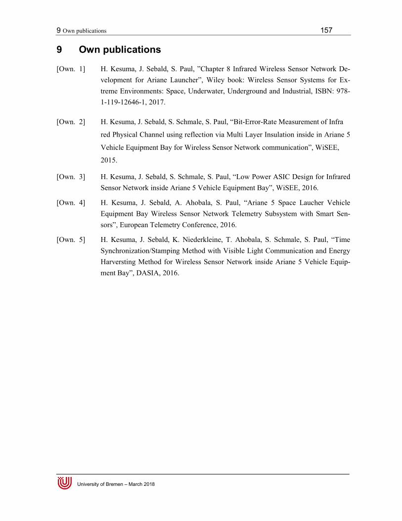
9 Own publications 157
University of Bremen – March 2018
9 Own publications
[Own. 1] H. Kesuma, J. Sebald, S. Paul, ”Chapter 8 Infrared Wireless Sensor Network De-velopment for Ariane Launcher”, Wiley book: Wireless Sensor Systems for Ex-treme Environments: Space, Underwater, Underground and Industrial, ISBN: 978-1-119-12646-1, 2017.
[Own. 2] H. Kesuma, J. Sebald, S. Schmale, S. Paul, “Bit-Error-Rate Measurement of Infra
red Physical Channel using reflection via Multi Layer Insulation inside in Ariane 5
Vehicle Equipment Bay for Wireless Sensor Network communication”, WiSEE,
2015.
[Own. 3] H. Kesuma, J. Sebald, S. Schmale, S. Paul, “Low Power ASIC Design for Infrared Sensor Network inside Ariane 5 Vehicle Equipment Bay”, WiSEE, 2016.
[Own. 4] H. Kesuma, J. Sebald, A. Ahobala, S. Paul, “Ariane 5 Space Laucher Vehicle Equipment Bay Wireless Sensor Network Telemetry Subsystem with Smart Sen-sors”, European Telemetry Conference, 2016.
[Own. 5] H. Kesuma, J. Sebald, K. Niederkleine, T. Ahobala, S. Schmale, S. Paul, “Time Synchronization/Stamping Method with Visible Light Communication and Energy Harversting Method for Wireless Sensor Network inside Ariane 5 Vehicle Equip-ment Bay”, DASIA, 2016.
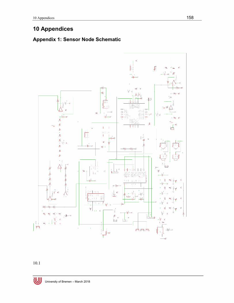
10 Appendices 158
University of Bremen – March 2018
10 Appendices
Appendix 1: Sensor Node Schematic
10.1
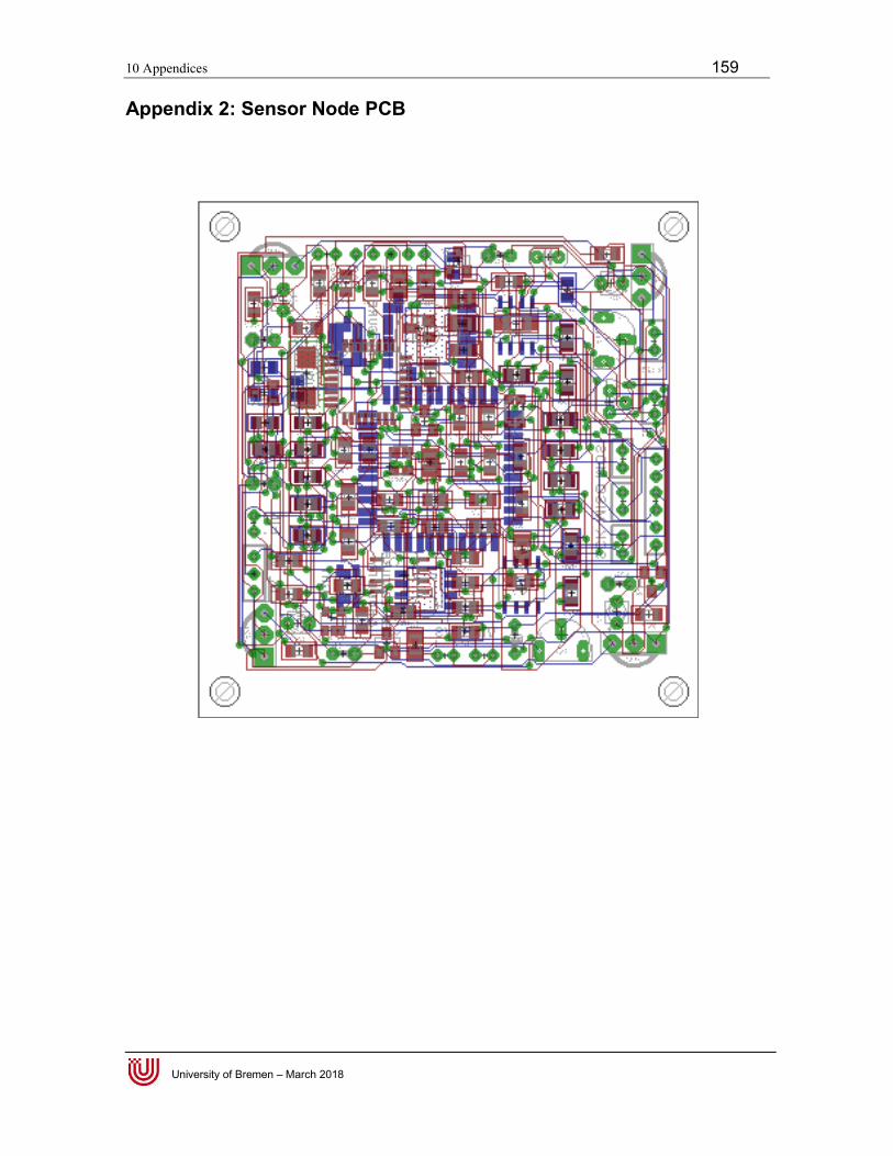
10 Appendices 159
University of Bremen – March 2018
Appendix 2: Sensor Node PCB
10 Appendices 160
University of Bremen – March 2018
Appendix 3: Infrared Receiver Schematic

10 Appendices 161
University of Bremen – March 2018
Appendix 4: Infrared Receiver PCB
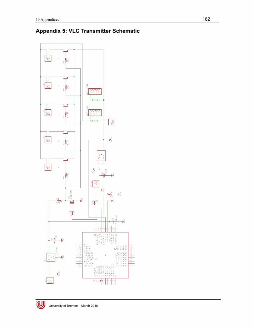
10 Appendices 162
University of Bremen – March 2018
Appendix 5: VLC Transmitter Schematic
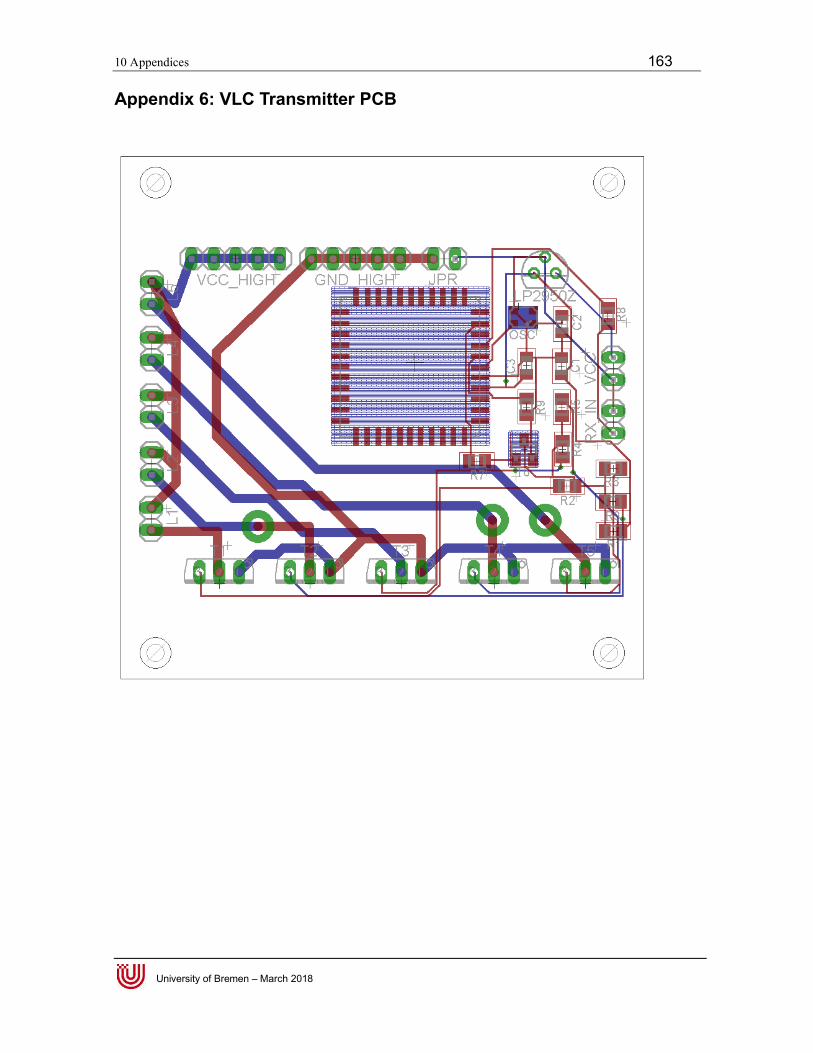
10 Appendices 163
University of Bremen – March 2018
Appendix 6: VLC Transmitter PCB