Embed Size (px)
Citation preview

Data Sheet Revision 2.0www.infineon.com 2018-12-06
BGA855N6
BGA855N6Low Noise Amplif ier for Lower L-Band GNSS Applications
Features
ApplicationThe BGA855N6 is designed to enhance GNSS signal sensitivity for band L2/L5 especially for very high accuracy.Besides GPS L5 and L2, the GNSS LNA also covers Galileo E5a, E5b, E6, Glonass G3, G2 and Beidou B3 and B2bands. The high linearity performance of BGA855N6 ensures best sensitivity for the operation in 4G & 5G NSAconfigurations.
Product ValidationQualified for industrial applications according to the relevant tests of JEDEC47/20/22
Block diagram
• Operating frequencies: 1164 - 1300 MHz• Insertion power gain: 17.8dB• Low noise figure: 0.60 dB• High linearity performance IIP3: 0 dBm• Low current consumption: 4.8 mA• Ultra small TSNP-6-10 leadless package (footprint: 0.7 x 1.1 mm2)• RF output internally matched to 50 Ohm• Only one external matching component needed• Specifically designed for:
- L2/L5 GPS Signals - E5a/E5b/E6 Galileo Signals - G2/G3 Glonass Signals - B2/B3 Beidou Signals
0.7 x 1.1 mm2
BGA855N6_Blockdiagram.vsd
AI AO
GND
ESD
VCC PON
Data Sheet 2 Revision 2.0 2018-12-06
BGA855N6Low Noise Amplifier for Lower L-Band GNSS Applications
Table of Contents
Table of Contents . . . . . . . . . . . . . . . . . . . . . . . . . . . . . . . . . . . . . . . . . . . . . . . . . . . . . . . . . . . . . . . . . . 2
1 Features . . . . . . . . . . . . . . . . . . . . . . . . . . . . . . . . . . . . . . . . . . . . . . . . . . . . . . . . . . . . . . . . . . . . . . . . . 3
2 Maximum Ratings . . . . . . . . . . . . . . . . . . . . . . . . . . . . . . . . . . . . . . . . . . . . . . . . . . . . . . . . . . . . . . . . . 5
3 Electrical Characteristics . . . . . . . . . . . . . . . . . . . . . . . . . . . . . . . . . . . . . . . . . . . . . . . . . . . . . . . . . . . 6
4 Application Information . . . . . . . . . . . . . . . . . . . . . . . . . . . . . . . . . . . . . . . . . . . . . . . . . . . . . . . . . . . . 9
5 Package Information . . . . . . . . . . . . . . . . . . . . . . . . . . . . . . . . . . . . . . . . . . . . . . . . . . . . . . . . . . . . . . 10
Table of Contents
Data Sheet 3 Revision 2.0 2018-12-06
BGA855N6Low Noise Amplifier for Lower L-Band GNSS Applications
Features
1 Features
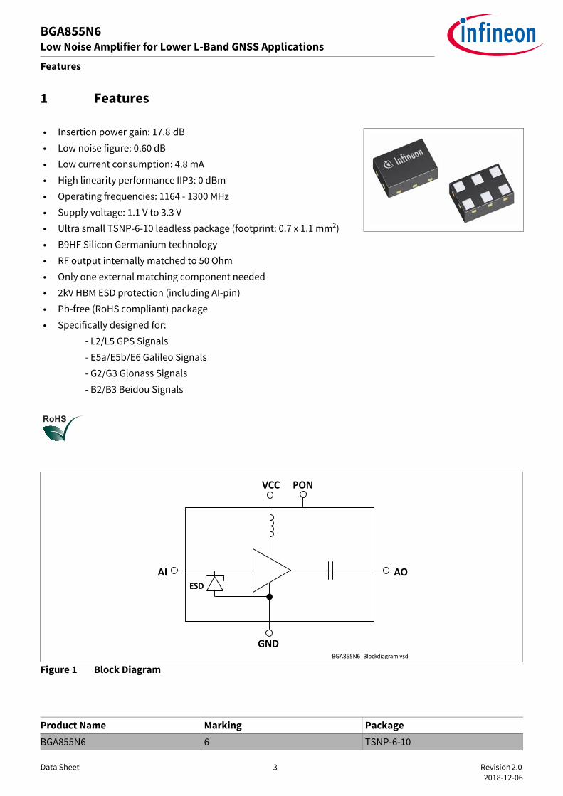
Figure 1 Block Diagram
• Insertion power gain: 17.8 dB• Low noise figure: 0.60 dB• Low current consumption: 4.8 mA• High linearity performance IIP3: 0 dBm• Operating frequencies: 1164 - 1300 MHz• Supply voltage: 1.1 V to 3.3 V• Ultra small TSNP-6-10 leadless package (footprint: 0.7 x 1.1 mm2)• B9HF Silicon Germanium technology• RF output internally matched to 50 Ohm• Only one external matching component needed• 2kV HBM ESD protection (including AI-pin)• Pb-free (RoHS compliant) package• Specifically designed for:
- L2/L5 GPS Signals - E5a/E5b/E6 Galileo Signals - G2/G3 Glonass Signals - B2/B3 Beidou Signals
Product Name Marking PackageBGA855N6 6 TSNP-6-10
BGA855N6_Blockdiagram.vsd
AI AO
GND
ESD
VCC PON

Data Sheet 4 Revision 2.0 2018-12-06
BGA855N6Low Noise Amplifier for Lower L-Band GNSS Applications
Features
DescriptionThe BGA855N6 is a front-end low noise amplifier for GPS L5 and L2, Galileo E5a, E5b, E6, Glonass G3, G2 andBeidou B3 and B2 bands for a frequency range from 1164 MHz to 1300 MHz. The LNA provides 17.8 dB gain and0.60 dB noise figure at a current consumption of 4.8 mA in the application configuration described in Chapter 4.The BGA855N6 is based upon Infineon Technologies‘ B9HF Silicon Germanium technology. It operates from 1.1 Vto 3.3 V supply voltage (device optimized for 1.8V operation / also prepared to support 1.2V and 2.8V operation).OFF-state can be enabled by PON pin.
Pin Definition and Function
Table 1 Pin Definition and FunctionPin No. Name Function1 GND Ground
2 VCC DC supply3 AO LNA output
4 GND Ground
5 AI LNA input6 PON Power On Control
Data Sheet 5 Revision 2.0 2018-12-06
BGA855N6Low Noise Amplifier for Lower L-Band GNSS Applications
Maximum Ratings
2 Maximum Ratings
Attention: Stresses above the max. values listed here may cause permanent damage to the device. Maximum ratings are absolute ratings; exceeding only one of these values may cause irreversible damage to the integrated circuit. Exposure to conditions at or below absolute maximum rating but above the specified maximum operation conditions may affect device reliability and life time. Functionality of the device might not be given under these conditions.
Table 2 Maximum RatingsParameter Symbol Values Unit Note or
Test ConditionMin. Typ. Max.Voltage at pin VCC1)
1) All voltages refer to GND-Node unless otherwise noted
VCC -0.3 – 3.6 V –Voltage at pin AI VAI -0.3 – 0.9 V –
Voltage at pin AO VAO -0.3 – VCC + 0.3 V –
Voltage at pin PON VPON -0.3 – VCC + 0.3 V –Voltage at pin GND VGND -0.3 – 0.3 V –
Current into pin VCC ICC – – 16 mA –
RF input power PIN – – +25 dBm –Total power dissipation, TS < 148 °C2)
2) TS is measured on the ground lead at the soldering point
Ptot – – 60 mW –
Junction temperature TJ – – 150 °C –
Ambient temperature range TA -40 – 85 °C –
Storage temperature range TSTG -55 – 150 °C –ESD capability all pins, HBM3)
3) Human Body Model ANSI/ESDA/JEDEC JS-001 (R = 1.5kΩ, C = 100pF)
VESD_HBM -2000 - +2000 V –
Data Sheet 6 Revision 2.0 2018-12-06
BGA855N6Low Noise Amplifier for Lower L-Band GNSS Applications
Electrical Characteristics
3 Electrical Characteristics
Table 3 Electrical Characteristics VCC = 1.2V1)
TA = 25 °C, VCC = 1.2 V, VPON = 1.2 V, f = 1164 - 1300 MHz
1) Based on the application described in Chapter 4
Parameter Symbol Values Unit Note or Test ConditionMin. Typ. Max.
Supply voltage VCC 1.1 1.2 3.3 V –
Supply current ICC – 4.4 5.4 mA ON Mode– 0.2 3 µA OFF Mode
Power on voltage VPON 1.0 – VCC V ON Mode
0 – 0.4 V OFF ModeSupply current IPON – 1.5 3 µA ON Mode
– – 1 µA OFF Mode
Insertion power gainf = 1214MHz
|S21|2 16.6 17.6 18.6 dB –
Noise figure2)
f = 1214 MHz, ZS = 50 Ω
2) PCB losses are subtracted
NF – 0.60 1.10 dB –
Input return loss3) f = 1214 MHz
3) Verification based on AQL; not 100% tested in production
RLIN 8 11 – dB –
Output return loss3) f = 1214 MHz
RLOUT 12 20 – dB –
Reverse isolation3)
f = 1214 MHz1/|S12|2 19 22 – dB –
Power on time4)7)
4) LNA Gain changed to 90% of final gain value (in dB)
tS – 3 5 µs OFF to ON ModeInband input 1dB-compression point, f = 1214 MHz3)
IP1dB -18 -14 – dBm –
Inband input 3rd-order intercept point3)5)
f1 = 1214 MHz, f2 = f1 +/- 1 MHz
5) Input power = -30 dBm for each tone
IIP3 -6 -1 – dBm –
Out of band input 3rd-order intercept point6)7)
f1 = 1850 MHz, f2 = 2500 MHz
6) Input power = -25 dBm for each tone
IIP3OOB -4 1 – dBm –
Stability7)
7) Guaranteed by device design; not tested in production
k > 1 – – f = 20 MHz ... 10 GHz

Data Sheet 7 Revision 2.0 2018-12-06
BGA855N6Low Noise Amplifier for Lower L-Band GNSS Applications
Electrical Characteristics
Table 4 Electrical Characteristics VCC = 1.8V1)
TA = 25 °C, VCC = 1.8 V, VPON = 1.8 V, f = 1164 - 1300 MHz
1) Based on the application described in Chapter 4
Parameter Symbol Values Unit Note or Test ConditionMin. Typ. Max.
Supply voltage VCC 1.1 1.8 3.3 V –
Supply current ICC – 4.8 5.8 mA ON Mode
– 0.2 3 µA OFF ModePower on voltage VPON 1.0 – VCC V ON Mode
0 – 0.4 V OFF Mode
Supply current IPON – 2.5 7.5 µA ON Mode– – 1 µA OFF Mode
Insertion power gainf = 1214MHz
|S21|2 16.8 17.8 18.8 dB –
Noise figure2)
f = 1214 MHz, ZS = 50 Ω
2) PCB losses are subtracted
NF – 0.60 1.10 dB –
Input return loss3) f = 1214 MHz
3) Verification based on AQL; not 100% tested in production
RLIN 9 12 – dB –
Output return loss3) f = 1214 MHz
RLOUT 12 20 – dB –
Reverse isolation3)
f = 1214 MHz1/|S12|2 19 22 – dB –
Power on time4)7)
4) LNA Gain changed to 90% of final gain value (in dB)
tS – 3 5 µs OFF to ON Mode
Inband input 1dB-compression point, f = 1214 MHz3)
IP1dB -15 -11 – dBm –
Inband input 3rd-order intercept point3)5)
f1 = 1214 MHz, f2 = f1 +/- 1 MHz
5) Input power = -30 dBm for each tone
IIP3 -5 0 – dBm –
Out of band input 3rd-order intercept point6)7)
f1 = 1850 MHz, f2 = 2500 MHz
6) Input power = -25 dBm for each tone
IIP3OOB -4 1 – dBm –
Stability7)
7) Guaranteed by device design; not tested in production
k > 1 – – f = 20 MHz ... 10 GHz

Data Sheet 8 Revision 2.0 2018-12-06
BGA855N6Low Noise Amplifier for Lower L-Band GNSS Applications
Electrical Characteristics
Table 5 Electrical Characteristics VCC = 2.8V1)
TA = 25 °C, VCC = 2.8 V, VPON = 2.8 V, f = 1164 - 1300 MHz
1) Based on the application described in Chapter 4
Parameter Symbol Values Unit Note or Test ConditionMin. Typ. Max.
Supply voltage VCC 1.1 2.8 3.3 V –
Supply current ICC – 5.4 6.4 mA ON Mode
– 0.2 3 µA OFF ModePower on voltage VPON 1.0 – VCC V ON Mode
0 – 0.4 V OFF Mode
Supply current IPON – 5 10 µA ON Mode– – 1 µA OFF Mode
Insertion power gainf = 1214MHz
|S21|2 16.9 17.9 18.9 dB –
Noise figure2)
f = 1214 MHz, ZS = 50 Ω
2) PCB losses are subtracted
NF – 0.60 1.10 dB –
Input return loss3) f = 1214 MHz
3) Verification based on AQL; not 100% tested in production
RLIN 10 13 – dB –
Output return loss3) f = 1214 MHz
RLOUT 12 20 – dB –
Reverse isolation3)
f = 1214 MHz1/|S12|2 19 22 – dB –
Power on time4)7)
4) LNA Gain changed to 90% of final gain value (in dB)
tS – 3 5 µs OFF to ON Mode
Inband input 1dB-compression point, f = 1214 MHz3)
IP1dB -12 -8 – dBm –
Inband input 3rd-order intercept point3)5)
f1 = 1214 MHz, f2 = f1 +/- 1 MHz
5) Input power = -30 dBm for each tone
IIP3 -4 1 – dBm –
Out of band input 3rd-order intercept point6)7)
f1 = 1850 MHz, f2 = 2500 MHz
6) Input power = -25 dBm for each tone
IIP3OOB -3 2 – dBm –
Stability7)
7) Guaranteed by device design; not tested in production
k > 1 – – f = 20 MHz ... 10 GHz

Data Sheet 9 Revision 2.0 2018-12-06
BGA855N6Low Noise Amplifier for Lower L-Band GNSS Applications
Application Information
4 Application Information
Application Board Configuration
Figure 2 Application Schematic BGA855N6
A list of all application notes is available at http://www.infineon.com/gpslna.appnotes
Table 6 Bill of MaterialsName Value Package Manufacturer FunctionC1 (optional) 1nF 0402 Various Input matching
C2 (optional) ≥ 1nF 0402 Various RF bypass 1)
1) RF bypass recommended to mitigate power supply noise
L1 9.4nH 0402 Murata LQW15 type Input matching
N1 BGA855N6 TSNP-6-10 Infineon SiGe LNA
BGA855N6_Schematic.vsd
N1 BGA855N6
AI, 5
PON, 6
GND, 4
GND, 1
AO, 3
VCC, 2
C1 (optional)L1
RFin
PON
VCC
C2(optional)
RFout

Data Sheet 10 Revision 2.0 2018-12-06
BGA855N6Low Noise Amplifier for Lower L-Band GNSS Applications
Package Information
5 Package Information
Figure 3 TSNP-6-10 Package Outline (top, side and bottom views)
Figure 4 Footprint Recommendation TSNP-6-10

Data Sheet 11 Revision 2.0 2018-12-06
BGA855N6Low Noise Amplifier for Lower L-Band GNSS Applications
Package Information
Figure 5 Marking Layout TSNP-6-10 (top view)
Figure 6 Date Code Marking TSNP-6-10
Figure 7 Tape & Reel Dimensions TSNP-6-10 (reel diameter 180 mm, pieces/reel 12000)
TSNP-6-10_MK.vsd
6
x x x x x x x x x x x x x x x x
Pin1 marking

Data Sheet 12 Revision 2.0 2018-12-06
BGA855N6Low Noise Amplifier for Lower L-Band GNSS Applications
Revision HistoryPage or Item Subjects (major changes since previous revision)Revision 2.0, 2018-12-06all Update to final status
4 Update Feature Description11 Update Tape and Reel Drawing
Other TrademarksAll referenced product or service names and trademarks are the property of their respective owners.
Edition 2018-12-06Published by Infineon Technologies AG81726 Munich, Germany
© 2018 Infineon Technologies AG.All Rights Reserved.
Do you have a question about any aspect of this document?Email: [email protected]
IMPORTANT NOTICEThe information given in this document shall in noevent be regarded as a guarantee of conditions orcharacteristics ("Beschaffenheitsgarantie"). With respect to any examples, hints or any typicalvalues stated herein and/or any information regardingthe application of the product, Infineon Technologieshereby disclaims any and all warranties and liabilitiesof any kind, including without limitation warranties ofnon-infringement of intellectual property rights of anythird party. In addition, any information given in this document issubject to customer's compliance with its obligationsstated in this document and any applicable legalrequirements, norms and standards concerningcustomer's products and any use of the product ofInfineon Technologies in customer's applications. The data contained in this document is exclusivelyintended for technically trained staff. It is theresponsibility of customer's technical departments toevaluate the suitability of the product for the intendedapplication and the completeness of the productinformation given in this document with respect tosuch application.
For further information on technology, delivery termsand conditions and prices, please contact the nearestInfineon Technologies Office (www.infineon.com).
WARNINGSDue to technical requirements products may containdangerous substances. For information on the typesin question please contact your nearest InfineonTechnologies office.
Except as otherwise explicitly approved by InfineonTechnologies in a written document signed byauthorized representatives of Infineon Technologies,Infineon Technologies’ products may not be used inany applications where a failure of the product or anyconsequences of the use thereof can reasonably beexpected to result in personal injury.
Please read the Important Notice and Warnings at the end of this document