Embed Size (px)
Citation preview
Low-Noise 24 GHz 0.15µm GaAs pHEMT Gilbert Cell Mixer for
Intelligent Transportation System Radar Receiver
By
Bashar Z. J. Asad
Thesis submitted to The Faculty of Graduate and Postdoctoral Studies in partial
fulfillment for the degree requirements of
Master of Applied Science
in
Electrical and Computer Engineering
Ottawa-Carleton Institute for Electrical and Computer Engineering
School of Electrical Engineering and Computer Science
University of Ottawa
Ottawa, Ontario, Canada
Copyright © Bashar Z.J. Asad, Ottawa, Canada, 2014

ii
ABSTRACT
Road traffic accidents are considered as the third cause of human deaths worldwide, while
leaving many others with severe injuries and/or in psychological and economical fragile
situations.
Therefore, several research works have been achieved to improve the reliability of transportation
systems. During the last few years, intelligent transportation systems (ITS) have been developed,
focusing on traffic-safety and traffic-assist systems, to name a few.
One of the most common ITS, that integrate between communications and information
technology, is the radar sensor working at 24 GHz.
In this work, the first mixer stage of a modified ITS radar receiver was designed with an output
intermediate frequency of 5.2 GHz, i.e., covering frequency bands accessible to emergency or
police services, two of the front-line services involved in road accidents.
The designed Gilbert cell mixer uses the 0.15 µm PHEMT GaAs technology. With a conversion
gain of 8.7 dB, a single sideband noise figure of 7 dB, a linearity of -13.5 dBm as well as an
isolation more than 30 dB, this mixer largely meets the Radar specifications.

iii
ACKNOWLEDGEMENTS
بسم هللا الرحمن الرحيم
First and foremost, I would like to give great thanks to my supervisor Prof. Mustapha C.E.
Yagoub who gave me this opportunity to join his research group at the University of Ottawa. I
really appreciate that. His keen knowledge, honest advises and great guidance have been the key
point to achieve this thesis and he is the good example I like to follow in my future.
I would like to thank my Co-supervisor Prof. Michel Nakhla for his support and encouragements
during this research work, I really appreciate that.
I would like to thank Professor Khelifa Hettak for his valuable guidance that is invaluable.
The thanks also given to Professor Roni Amaya for giving me the GaAs pHEMT Technology
that has been used in this thesis.
Last but the most I would like to thank my family and my friends for their support and
encouragements during this thesis work.

iv
TABLE OF CONTENTS
List of Figures ................................................................................................................................ vi
List of Tables ................................................................................................................................. xi
List of Acronyms and Abbreviations ............................................................................................ xii
CHAPTER 1 INTRODUCTION ................................................................................................... 1
1.1 Motivation ............................................................................................................................. 1
1.2 Thesis Contribution ............................................................................................................... 3
1.3 Thesis Organization............................................................................................................... 3
CHAPTER 2 RADAR RECEIVER ................................................................................................ 5
2.1 Radar Types and Selection .................................................................................................... 5
2.2 Radar Equations .................................................................................................................... 6
2.3 Wireless Communications System Architectures ................................................................. 7
2.4 Radar Receiver Design and Link Budget Analysis ............................................................. 11
2.4.1Modified radar receiver ................................................................................................. 11
2.4.2 Link budget analysis ..................................................................................................... 11
2.5 Conclusion ........................................................................................................................... 16
CHAPTER 3 MIXER THEORY AND CONFIGURATIONS .................................................... 17
3.1 Mixer Theory....................................................................................................................... 17
3.2 Mixer Characteristics .......................................................................................................... 18
3.2.1 Conversion gain ............................................................................................................ 18
3.2.2 Noise figure................................................................................................................... 18
3.2.3 Isolation ........................................................................................................................ 21
3.2.4 Linearity........................................................................................................................ 21
3.2.5 Dynamic range ............................................................................................................. 27
3.3 Mixer Topologies ................................................................................................................ 30
3.3.1 Passive mixers ............................................................................................................. 30
3.3.2 Active mixers ................................................................................................................. 33
3.4 Gilbert Cell Mixer Design ................................................................................................... 36
3.5 Conclusion ........................................................................................................................... 39

v
CHAPTER 4 COUPLER DESIGN .............................................................................................. 40
4.1 Introduction ......................................................................................................................... 40
4.2 24 GHz Rat-Race Coupler Design ..................................................................................... 42
4.2.1 Ideal design................................................................................................................... 42
4.2.2 Layout design ................................................................................................................ 43
4.3 18.8 GHz Rat-Race Coupler Design .................................................................................. 47
4.4 5.2GHz Rat- Race Coupler Design .................................................................................... 48
4.5 Conclusion .......................................................................................................................... 49
CHAPTER 5 MIXER DESIGN .................................................................................................... 50
5.1 Proposed Gilbert Cell Mixer ............................................................................................... 51
5.2 Transistor Sizing ................................................................................................................. 53
5.2.1 Transistor sizing for the RF-LO stages ........................................................................ 53
5.2.2 Transistor sizing for the source follower stage ............................................................ 55
5.2.3 Transistor sizing for the current mirror ....................................................................... 55
5.3 DC Analysis ........................................................................................................................ 55
5.4 Mixer Schematic ................................................................................................................. 58
5.5 CO-Simulation .................................................................................................................... 64
5.6 Discussion ........................................................................................................................... 72
5.7 Conclusion ........................................................................................................................... 79
CHAPTER 6 CONCLUSION AND FUTURE WORK ............................................................... 80
6.1 Conclusion .......................................................................................................................... 80
6.2 Future Work ....................................................................................................................... 80
REFERENCES ............................................................................................................................. 83
APPENDIX .................................................................................................................................. 93

vi
LIST OF FIGURES
Figure (1.1) Some vehicles benefits from ITS ........................................................................... 2
Figure (2.1) Monostatic and bistatic radar antenna ..................................................................... 6
Figure (2.2) Wave propagation for radar sensing. ...................................................................... 6
Figure (2.3) Simplified homodyne receiver ................................................................................ 8
Figure (2.4) Simplified super heterodyne receiver ..................................................................... 9
Figure (2.5) Effect of image at high IF ..................................................................................... 10
Figure (2.6) Effect of image frequency at low IF ..................................................................... 10
Figure (2.7) 24 GHz Modified Radar receiver .......................................................................... 11
Figure (2.8) 24 GHz radar receiver link budget analysis .......................................................... 14
Figure (3.1) Fundamental mixer block diagram ....................................................................... 17
Figure (3.2) Noise spectral density ........................................................................................... 19
Figure (3.3) (a) Single sideband noise figure, (b) Double sideband noise ............................... 20
Figure (3.4) Leakage directions between the ports ................................................................... 21
Figure (3.5) Intermodulation spectrum representations ............................................................ 22
Figure (3.6) P1-dB compression point ...................................................................................... 24
Figure (3.7) IP2, and IP3 compression points ........................................................................... 26
Figure (3.8) Third order intermodulation spectrum .................................................................. 27
Figure (3.9) Dynamic range ...................................................................................................... 29
Figure (3.10) Single diode mixer ................................................................................................ 31
Figure (3.11) Single balanced diode mixer ................................................................................. 31
Figure (3.12) Double balance mixer ........................................................................................... 32

vii
Figure (3.13) FET Resistive Mixer ............................................................................................. 32
Figure (3.14) The general structure of a gate mixer ................................................................... 33
Figure (3.15) Dual Gate mixer .................................................................................................... 34
Figure (3.16) Single balanced mixer ........................................................................................... 34
Figure (3.17) Single active balanced mixer representation ......................................................... 35
Figure (3.18) Fundamental Gilbert cell mixer parts ................................................................... 36
Figure (3.19) Gilbert cell mixer basic structure .......................................................................... 37
Figure (4.1) Hybrid Rat-Race coupler ...................................................................................... 40
Figure (4.2) Ideal 24 GHz rat-race coupler schematic .............................................................. 43
Figure (4.3) Simulated coupling ............................................................................................... 44
Figure (4.4) Simulated amplitude imbalance ............................................................................ 44
Figure (4.5) Simulated isolation and input return loss .............................................................. 44
Figure (4.6) Simulated phase imbalance ................................................................................... 44
Figure (4.7) 24 GHz rat- race coupler: transmission line schematic ........................................ 45
Figure (4.8) 24 GHz rat- race coupler layout ............................................................................ 45
Figure (4.9) Simulated coupling ............................................................................................... 46
Figure (4.10) Simulated amplitude imbalance ............................................................................ 46
Figure (4.11) Simulated isolation and input return loss .............................................................. 46
Figure (4.12) Simulated phase imbalance ................................................................................... 46
Figure (4.13) Simulated coupling ............................................................................................... 47
Figure (4.14) Simulated amplitude imbalance ............................................................................ 47
Figure (4.15) Simulated isolation and input return loss .............................................................. 47
Figure (4.16) Simulated phase imbalance ................................................................................... 47
Figure (4.17) Simulated coupling ............................................................................................... 48
viii
Figure (4.18) Simulated amplitude imbalance ............................................................................ 48
Figure (4.19) Simulated isolation and input return loss .............................................................. 48
Figure (4.20) Simulated phase imbalance ................................................................................... 48
Figure (4.21) Simulated coupling ............................................................................................... 49
Figure (4.22) Simulated amplitude imbalance ............................................................................ 49
Figure (4.23) Simulated isolation and input return loss .............................................................. 49
Figure (4.24) Simulated phase imbalance ................................................................................... 49
Figure (5.1) 24 GHz Gilbert Cell mixer: proposed schematic. ................................................. 51
Figure (5.2) Current bleeding technique ................................................................................... 53
Figure (5.3) Simulated minimum noise figure over drain current ............................................ 54
Figure (5.4) Simulated unity current gain frequency (ft) .......................................................... 54
Figure (5.5) Threshold voltage curve for the 0.15µ pHEMT GaAs technology . .................... 56
Figure (5.6) Differential pair bias point ................................................................................... 56
Figure (5.7) Switching stage transistor bias point.................................................................... 57
Figure (5.8) Depletion mode current mirror ............................................................................ 57
Figure (5.9) Current mirror bias point ..................................................................................... 58
Figure (5.10) Common drain (buffer stage) transistor bias point ............................................... 58
Figure (5.11) Gilbert mixer schematic including the couplers ................................................... 59
Figure (5.12) Final configuration: Mixer with couplers and input/output matching networks . 59
Figure (5.13) Simulated SSB noise figure versus LO power ...................................................... 60
Figure (5.14) Simulated conversion gain versus LO power ....................................................... 60
Figure (5.15) Simulated linearity versus RF power .................................................................... 61
Figure (5.16) Simulated SSB noise figure versus input RF frequency ....................................... 61
Figure (5.17) Simulated conversion gain versus input RF frequency ......................................... 62
ix
Figure (5.18) Simulated leakage versus input RF frequency ...................................................... 62
Figure (5.19) Simulated return losses: (a) at the input, (b) at the output .................................... 63
Figure (5.20) Simulated mixer spectrum: (a) at the input, (b) at the output. .............................. 64
Figure (5.21) 24 GHz Gilbert Cell Mixer Layout ....................................................................... 66
Figure (5.22) Simulated noise figure versus LO Power .............................................................. 67
Figure (5.23) Simulated gain versus LO power .......................................................................... 67
Figure (5.24) Simulated 1-dB Compression Point Versus RF Input power ............................... 68
Figure (5.25) Simulated noise figure versus input RF frequency ............................................... 68
Figure (5.26) Simulated gain versus input RF frequency. .......................................................... 69
Figure (5.27) Simulated Leakage versus RF Frequency ............................................................. 69
Figure (5.28) Simulated mixer spectrum: (a) at the input, (b) at the output ............................... 70
Figure (5.29) Simulated return losses: (a) at the input, (b) at the output .................................... 71
Figure (5.30) Noise figure curves for both schematic and layout over LO power. .................... 72
Figure (5.31) Conversion gain curves for both schematic and layout over LO power. .............. 73
Figure (5.32) Noise figure curves for both schematic and layout over RF frequency. ............... 73
Figure (5.33) Conversion gain curves for both schematic and layout over RF frequency . ....... 74
Figure (5.34) Conversion gain curves for both schematic and layout over RF power. .............. 74
Figure (5.35) Isolation between LO-RF ports over RF frequency. ............................................. 75
Figure (5.36) Isolation between LO-IF ports over RF frequency. .............................................. 75
Figure (5.37) Isolation between RF-IF ports over RF frequency. .............................................. 76
Figure (5.38) Isolation between the LO-RF ports over LO power. ............................................ 76
Figure (6.1) Parasitic positions in single balanced mixer. ........................................................ 81
Figure (A.1) Receiver schematic ............................................................................................... 93
Figure (A.2) The attenuations values for the 3, 4, 5 dB attenuators .......................................... 97
x
Figure (A.3) NF, gain, P1dB, and OIP3 specifications for ADL 5542 ...................................... 98
Figure (A.4) (BFCN-2900+) electrical specifications ............................................................. 101
Figure (B.1) GaAs substrate layers. ......................................................................................... 102
Figure (B.2) SiN substrate layers. ............................................................................................ 103
Figure (B.3) Air substrate layers. ............................................................................................. 104
xi
LIST OF TABLES
Table (2.1) System specifications of the 24-GHz system .......................................................... 12
Table (2.2) Link budget analysis for 24-GHz system. ............................................................... 13
Table (2.3) Mixer specifications ................................................................................................ 15
Table (3.1) Summary of distortion components......................................................................... 23
Table (4.1) Conventional rat- race Coupler operation ............................................................... 42
Table (5.1) Gilbert Cell Mixer Specifications ............................................................................ 50
Table (5.2) Layout, schematic and design specifications comparisons ..................................... 77
Table (5.3) Performance comparison with published works...................................................... 78
Table (A.1) HMC 751 parameters............................................................................................... 95

xii
LIST OF ACRONYMS AND ABBREVIATIONS
BB Base Band.
BPF Band pass filter.
DSB Double side band.
F Noise factor.
ft Unity current gain frequency .
GaAs Gallium Arsenide.
G Gain.
Gm Transconductance.
IF Intermediate Frequency.
IIP3 Third order input intercept point.
IMD Intermodulation distortion.
ITS Intelligent Transportation System.
LNA Low noise amplifier.
LO Local Oscillator.
MMIC Monolithic Microwave Integrated Circuit.
NF Noise figure.
OIP Output intercept point.
P1-dB 1-dB compression point.
PHEMT High Electron Mobility Transistor.
RF Radio Frequency.
SNR Signal to noise ratio.
SSB Single Side Band.

1
Chapter 1
Introduction
1.1 Motivations
With about 1.2 million deaths on the roads, road crashes are considers as the third leading
cause of death in the world. When it comes to Canada, five to six persons are dying daily
because of road accidents [1], [2]. In parallel, road traffic injuries have social and economic
costs, psychological effects, and lots of care should be given to the injured people by their
families or by special caregivers.
On the other hand, road crashes are very expensive in terms of both material cost (damages to
vehicles and infrastructures) and human cost for treatment of injured/disabled people. So road
accidents have received unprecedented attention and the safety in transportation systems
becomes a global concern [2].
A recent joint report launched by the World Health Organization (WHO) and the World Bank,
demonstrates that much could be done to increase the safety on the roads and to reduce the toll of
deaths and injuries [1].
Increasing road safety and enhancing the transportation system involve improving services to
travelers, helping meeting targets related to journey time reliability, providing real-time
information to assist route planning, reducing congestions and subsequently road accidents,
pollution, travel time, travel cost, and greenhouse gases, while increasing traffic mobility and
economic productivity. These enhancements and improvements lead to the design of Intelligent
Transportation Systems (ITS) [3]-[5] (Figure (1.1), [5]).
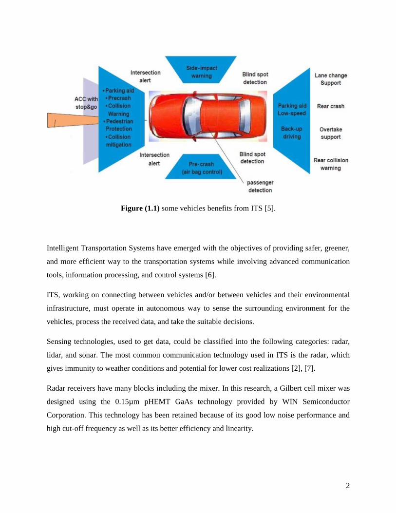
2
Figure (1.1) some vehicles benefits from ITS [5].
Intelligent Transportation Systems have emerged with the objectives of providing safer, greener,
and more efficient way to the transportation systems while involving advanced communication
tools, information processing, and control systems [6].
ITS, working on connecting between vehicles and/or between vehicles and their environmental
infrastructure, must operate in autonomous way to sense the surrounding environment for the
vehicles, process the received data, and take the suitable decisions.
Sensing technologies, used to get data, could be classified into the following categories: radar,
lidar, and sonar. The most common communication technology used in ITS is the radar, which
gives immunity to weather conditions and potential for lower cost realizations [2], [7].
Radar receivers have many blocks including the mixer. In this research, a Gilbert cell mixer was
designed using the 0.15µm pHEMT GaAs technology provided by WIN Semiconductor
Corporation. This technology has been retained because of its good low noise performance and
high cut-off frequency as well as its better efficiency and linearity.
3
1.2 Thesis Contributions
In this thesis, the main contribution has been to propose a modified configuration of a 24 GHz
radar receiver for intelligent transportation systems (ITS). With two conversion stages, the
suggested receiver configuration approach increases the ability for image rejection while
reducing its sensitivity to DC offset, figure noise and second order intermodulation. The first
mixer converts the input 24 GHz to 5.2 GHz, thus giving direct access to WLAN systems used
by emergency or police cars. The second conversion stage will give access to Next Generation
Weather Radar (NEXRAD) systems that use the 2.7-3.1 GHz frequency band for meteorological
purposes and whether forecast
Designing the first mixer while meeting the ITS/WLAN standards was the second contribution
of the present work. The circuit was designed using the 0.15 µm GaAs PHEMT low noise
technology, thus assuring the desired high dynamic range and low noise.
1.3 Thesis Organization
The content of this thesis is divided into six chapters. After this introductory Chapter,
Chapter 2 provides general information about radar receivers used in ITS, particularly in the 24
GHz ISM band. Then, the radar receiver link budget is discussed.
Chapter 3 introduces the basic mixer design parameters and the different types of mixers. Then,
the advantages of the Gilbert cell mixer over other types of mixers are highlighted.
Chapter 4 presents the design of three microstrip hybrid couplers required at the mixer ports. In
fact, beside the mixer itself, three 3dB 180o micro strip couplers were designed, i.e., one for each
of the three mixer ports (RF, IF, LO); two of them convert the two single input signals (RF and
LO) to differential ones while the third coupler combines the output differential signals to a
single IF signal.
Chapter 5 presents the design process of the Gilbert cell mixer. Both schematic and layout
simulations were performed and compared, leading to a successful mixer design, largely meeting
the required specs.

4
Finally, Chapter 6 summarizes the contents of this thesis and provides ideas for future research
on the topics discussed in this thesis.
5
Chapter 2
Radar Receiver
2.1 Radar Types and Selection
Radar is the most promising and robust solution to vehicle sensing requirements in terms of
environmental conditions, measurement capabilities, and ease of installation. The best frequency
to use for radar depends upon the targeted application. In fact, this choice of frequency involves
trade-offs between several factors such as transmitted and received powers, physical receiver
size, antenna beam width, and atmospheric attenuation. Radars for vehicle applications usually
use two frequencies: 77 GHz and 24 GHz; this later being the most used because of its higher
reliability, accuracy, and sensitivity over the 77 GHz. Also, 24 GHz radar is easier to handle; its
level gauge is smaller and is more suitable for high directivity antenna array systems. It has also
better performance in azimuth angle and in range measurements, thus, suitable for automotive
applications like parking aid, pre-crash detection, and blind spot detection [8]-[10].
A radar is a complex electronic and electromagnetic system constituted by a transmitter, receiver
and antenna. It is composed of many different sub-systems, themselves composed of many
different components. The basic principle behind the radar depends on bursts of radio energy
transmitted into the air “these bursts are electromagnetic (EM) waves at microwave frequencies.
If there is an object in the path of the radio wave, it reflects some of the electromagnetic energy,
and the radio wave will bounce back to the radar device” [11].
With respect to the radar itself, the transmitter and the receiver could have two separate antennas,
thus called bistatic radar. A radar having same antenna for both transmitter and receiver, is called
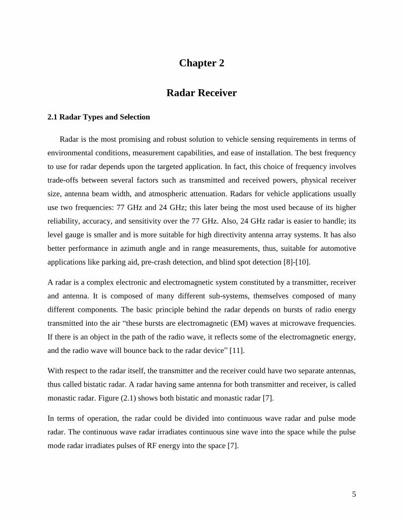
monastic radar. Figure (2.1) shows both bistatic and monastic radar [7].
In terms of operation, the radar could be divided into continuous wave radar and pulse mode
radar. The continuous wave radar irradiates continuous sine wave into the space while the pulse
mode radar irradiates pulses of RF energy into the space [7].
6
In terms of covered area or distance that can be reached, the radar can be divided into short range
radar, medium range radar, and long range radar. Short range radar works in pulse mode and has
wide horizontal angular coverage with a covered distance of about 30 meters. It also requires
wide bandwidth. Medium range radar works at continuous wave mode with a distance up to
approximately 70 meters. It uses a narrow ISM band system, and the angular coverage is from
40o to 50
o. Long range radar works in continuous wave mode. It uses a narrow bandwidth and an
angular coverage from 4o to 8
o with a covered distance of about 200 meters [7].
Figure (2.1) Monostatic and bistatic radar antenna [7].
2.2 Radar Equations
The ability of a radar to detect the presence of a target is expressed in terms of radar
equations used to predict the echo power and the interfering power. They help designing the
radar to meet the required specifications, establishing the relationship between the power of the
received signal and the target parameters, and providing means of predicting signal-to-noise
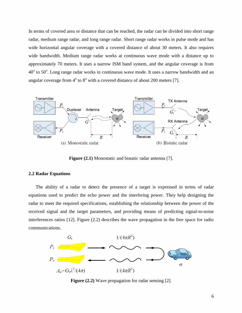
interferences ratios [12]. Figure (2.2) describes the wave propagation in the free space for radio
communications.
Figure (2.2) Wave propagation for radar sensing [2].

7
The relationship between the peak transmitted power Pt and the received power Pr, also called
bistatic equation, is presented by
( )
(2.1)
In this equation, Gt and Gr represent the transmitter and received gain, respectively. λ is the radar
operation wavelength and σ the target non fluctuating cross section. L is the general loss factor
that accounts for both system and propagating losses. Rt and Rr state for the distance between the
target and respectively the transmitter and the receiver. If the radar is monastic, the transmitter
and receiver distances are identical [13].
In real conditions, there is a difference between the received signal power and the transmitter
signal power due to factors like loss in the transmitted signal (from the transmitter to the
antenna), loss in the received signal (from the antenna to the receiver), attenuation of the signal
through the atmosphere, etc. [14]
( ) (2.2)
with the power radiated by the antenna, G the antenna gain, R the distance from radar to the
target, the effective noise temperature, λ the operating wavelength, and σ the radar target
cross section. F is the receiver noise factor and the equivalent noise bandwidth (Hz).
2.3 Wireless Communications System Architectures
The architectures of the receiver could be classified upon the topology of the down
conversion: homodyne receiver and super heterodyne receiver.
The homodyne receiver, or direct conversion receiver, converts the input radio frequency (RF) to
the zero intermediate frequency (IF), which means that the input frequency (radio frequency) is
equal to the local oscillator frequency (LO). Figure (2.3) shows a simplified homodyne receiver.

8
Figure (2.3) Simplified homodyne receiver [15].
This topology holds some advantages and disadvantages. The main advantage of this receiver is
that it does not need a band-pass filter between the low noise amplifier and the mixer to reject the
image frequency because the image is the signal itself. It also usually uses a quadrature mixing
configuration to separate the upper sideband signal from the lower sideband one (the quadrature
topology helps removing the problem of phase mismatch between the input frequency and the
local oscillator frequency). The homodyne receiver uses the double sideband to reconstruct the
desired signal in the baseband and allows high level of integration and high performance [16]-
[18].
The first disadvantage of this topology is the DC offset. In fact, the DC offset at the baseband
frequency, whether due to self-mixing or mismatches will be amplified by the large gain present
at the baseband chain. Another issue is the flicker noise. This is primarily due to the fact that the
signal has not been significantly amplified before encountering the high flicker noise region of
the receiver. Also, the non-linearity of the homodyne receiver is characterized by the 2nd
order
intermodulation distortion [16], [17] and more stringent dynamic range and reverse isolation.
The frequency drift problem is also a constraint, where the small drift can cause the direct
conversion receiver to become unstable [18], [19].
The second receiver topology is the super heterodyne receiver. In this most widely used
topology, the input frequency (RF) is converted to a non-zero intermediate frequency (IF) [19].
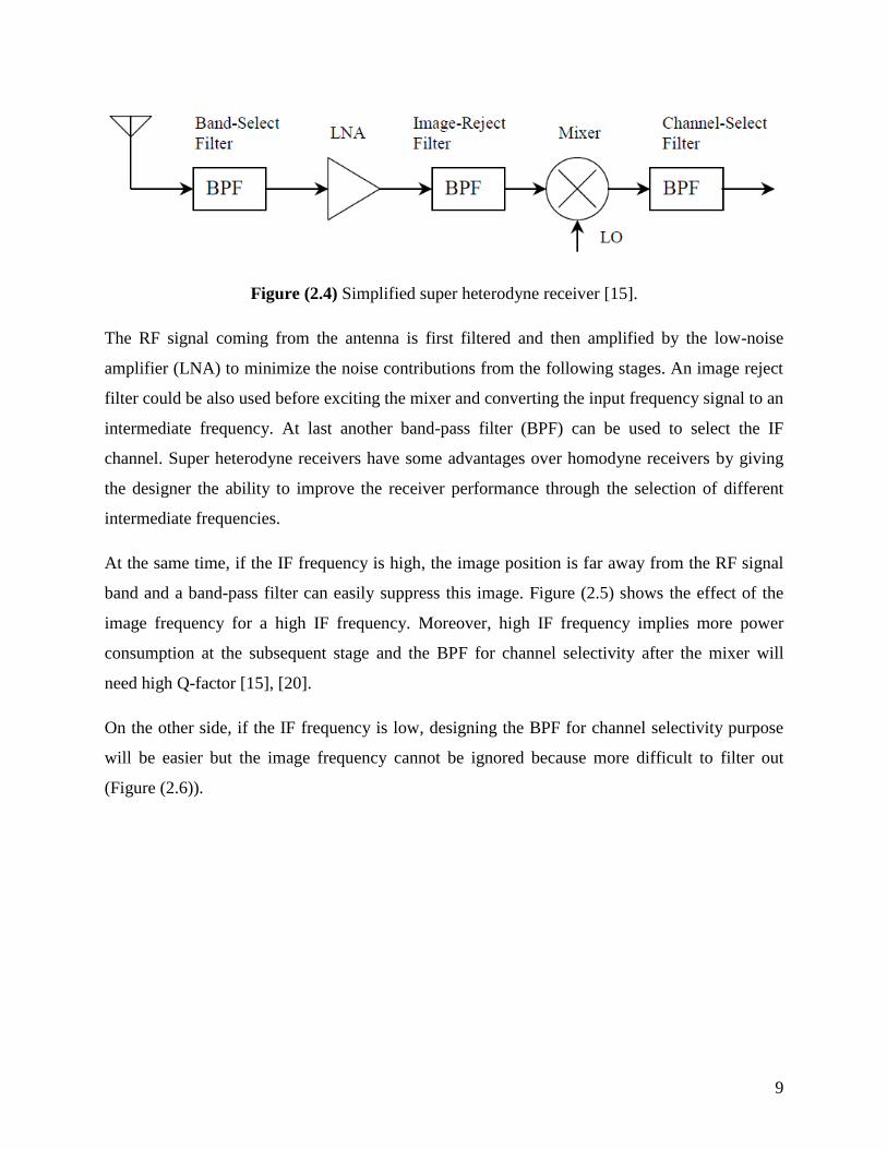
Figure (2.4) shows a simplified super heterodyne receiver.
9
Figure (2.4) Simplified super heterodyne receiver [15].
The RF signal coming from the antenna is first filtered and then amplified by the low-noise
amplifier (LNA) to minimize the noise contributions from the following stages. An image reject
filter could be also used before exciting the mixer and converting the input frequency signal to an
intermediate frequency. At last another band-pass filter (BPF) can be used to select the IF
channel. Super heterodyne receivers have some advantages over homodyne receivers by giving
the designer the ability to improve the receiver performance through the selection of different
intermediate frequencies.
At the same time, if the IF frequency is high, the image position is far away from the RF signal
band and a band-pass filter can easily suppress this image. Figure (2.5) shows the effect of the
image frequency for a high IF frequency. Moreover, high IF frequency implies more power
consumption at the subsequent stage and the BPF for channel selectivity after the mixer will
need high Q-factor [15], [20].
On the other side, if the IF frequency is low, designing the BPF for channel selectivity purpose
will be easier but the image frequency cannot be ignored because more difficult to filter out
(Figure (2.6)).

10
Figure (2.5) Effect of image at high IF [15].
Figure (2.6) Effect of image frequency at low IF [15].
So to alleviate the problem between low and high IF frequencies, a dual conversion receiver can
be proposed with double-conversion stages in super heterodyne receiver allowing higher IF for
the first conversion stage (so that the image is easier to filter out) and allowing lower IF for the
second stage (for better channel selectivity) [15], [21].
So for these aforementioned advantages for super heterodyne receiver, a modified dual
conversion super heterodyne receiver for radar applications is proposed in this thesis.
11
2.4 Radar Receiver Design and Link Budget Analysis
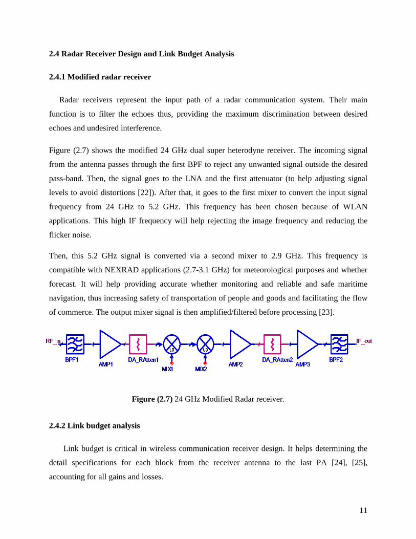
2.4.1 Modified radar receiver
Radar receivers represent the input path of a radar communication system. Their main
function is to filter the echoes thus, providing the maximum discrimination between desired
echoes and undesired interference.
Figure (2.7) shows the modified 24 GHz dual super heterodyne receiver. The incoming signal
from the antenna passes through the first BPF to reject any unwanted signal outside the desired
pass-band. Then, the signal goes to the LNA and the first attenuator (to help adjusting signal
levels to avoid distortions [22]). After that, it goes to the first mixer to convert the input signal
frequency from 24 GHz to 5.2 GHz. This frequency has been chosen because of WLAN
applications. This high IF frequency will help rejecting the image frequency and reducing the
flicker noise.
Then, this 5.2 GHz signal is converted via a second mixer to 2.9 GHz. This frequency is
compatible with NEXRAD applications (2.7-3.1 GHz) for meteorological purposes and whether
forecast. It will help providing accurate whether monitoring and reliable and safe maritime
navigation, thus increasing safety of transportation of people and goods and facilitating the flow
of commerce. The output mixer signal is then amplified/filtered before processing [23].
Figure (2.7) 24 GHz Modified Radar receiver.
2.4.2 Link budget analysis
Link budget is critical in wireless communication receiver design. It helps determining the
detail specifications for each block from the receiver antenna to the last PA [24], [25],
accounting for all gains and losses.
12
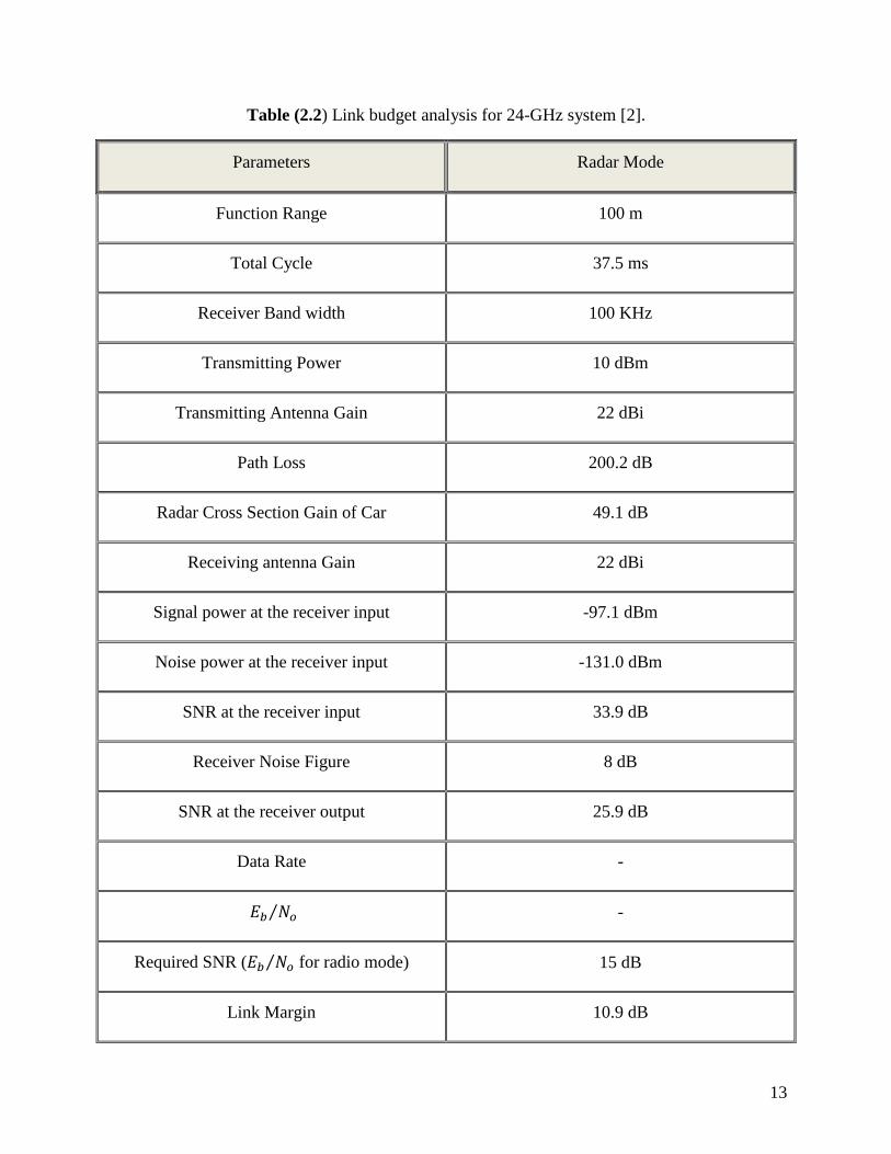
In 24 GHz automotive radar applications, the requirements are based on the FCC’s standards [2],
summarized in Table (2.1), while the corresponding link budget analysis is reported in Table
(2.2). From these tables, the radar will be long range radar type with a bandwidth of 100 kHz.
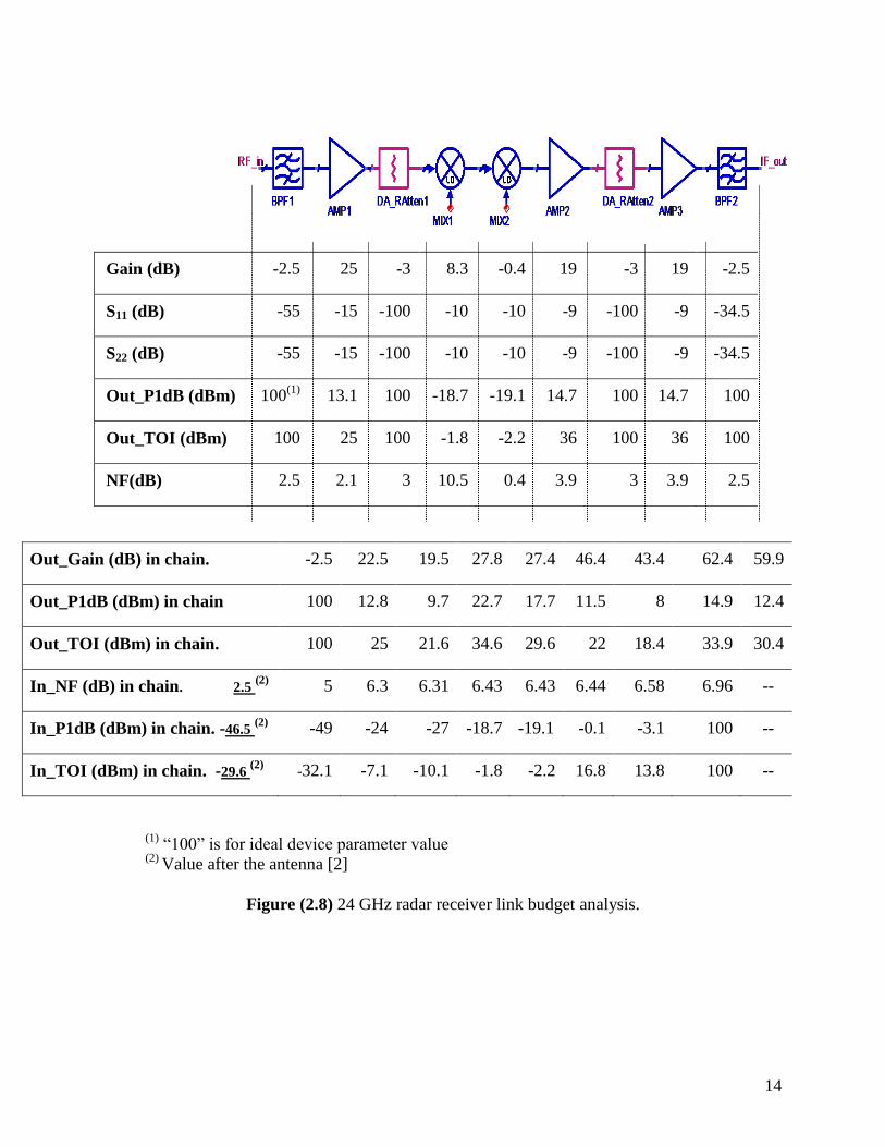
In order to meet the radar specifications, the link budget of the receiver was evaluated. The
required values for each block of the receiver have been selected carefully to meet the
specifications for the radar receiver (Figure (2.8), with details given in the appendix).
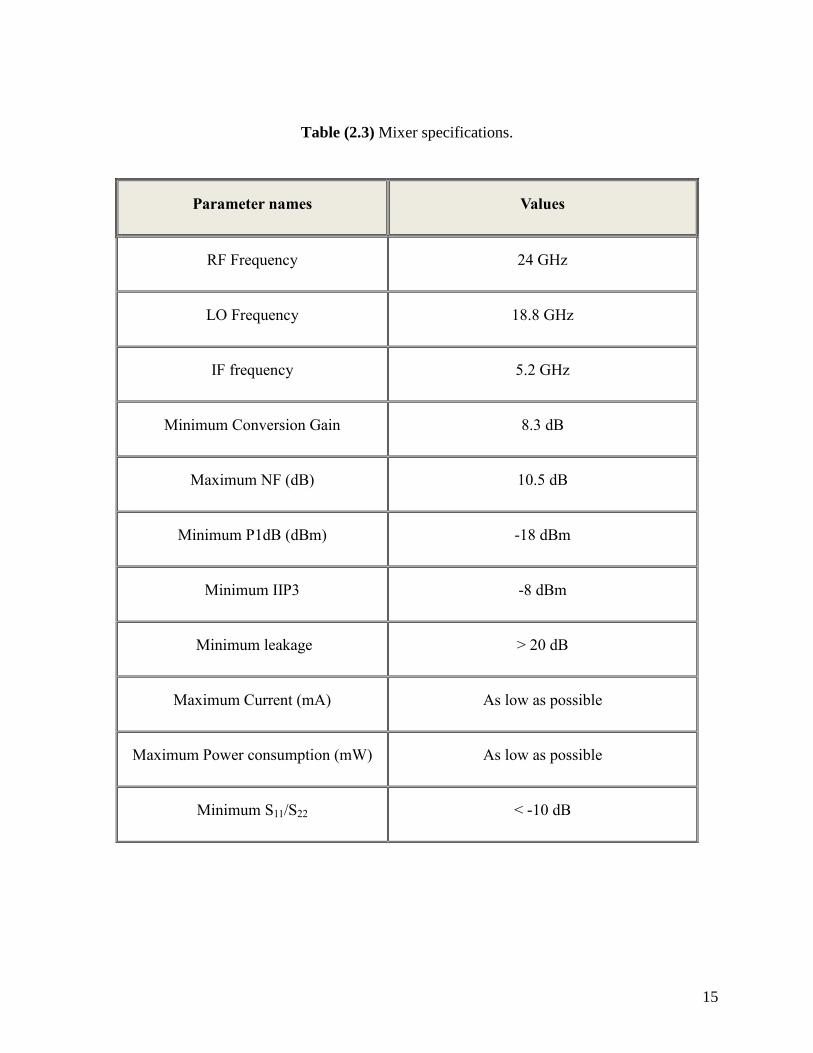
Because in this work concentrate on the first mixer, its design parameters (obtained from the link
budget) are summarized in Table (2.3).
Table (2.1) System specifications of the 24-GHz system [2].
Mode Specifications Values
Radar
Frequency Range 24.075 to 24.175 GHz
Maximum Detectable Range 100 m
Range resolution 1.5 m
Maximum Detectable Velocity ± 260 km/h (69.44m/s)
Velocity Resolution ± 1.8 km/h (0.5m/s)
Probability of False Alarm 1e-6
Probability of Detection 0.9
13
Table (2.2) Link budget analysis for 24-GHz system [2].
Parameters Radar Mode
Function Range 100 m
Total Cycle 37.5 ms
Receiver Band width 100 KHz
Transmitting Power 10 dBm
Transmitting Antenna Gain 22 dBi
Path Loss 200.2 dB
Radar Cross Section Gain of Car 49.1 dB
Receiving antenna Gain 22 dBi
Signal power at the receiver input -97.1 dBm
Noise power at the receiver input -131.0 dBm
SNR at the receiver input 33.9 dB
Receiver Noise Figure 8 dB
SNR at the receiver output 25.9 dB
Data Rate -
⁄ -
Required SNR ( ⁄ for radio mode) 15 dB
Link Margin 10.9 dB
14
Gain (dB) -2.5 25 -3 8.3 -0.4 19 -3 19 -2.5
S11 (dB) -55 -15 -100 -10 -10 -9 -100 -9 -34.5
S22 (dB) -55 -15 -100 -10 -10 -9 -100 -9 -34.5
Out_P1dB (dBm) 100(1)
13.1 100 -18.7 -19.1 14.7 100 14.7 100
Out_TOI (dBm) 100 25 100 -1.8 -2.2 36 100 36 100
NF(dB) 2.5 2.1 3 10.5 0.4 3.9 3 3.9 2.5
Out_Gain (dB) in chain. -2.5 22.5 19.5 27.8 27.4 46.4 43.4 62.4 59.9
Out_P1dB (dBm) in chain 100 12.8 9.7 22.7 17.7 11.5 8 14.9 12.4
Out_TOI (dBm) in chain. 100 25 21.6 34.6 29.6 22 18.4 33.9 30.4
In_NF (dB) in chain. 2.5 (2)
5 6.3 6.31 6.43 6.43 6.44 6.58 6.96 --
In_P1dB (dBm) in chain. -46.5 (2)
-49 -24 -27 -18.7 -19.1 -0.1 -3.1 100 --
In_TOI (dBm) in chain. -29.6 (2)
-32.1 -7.1 -10.1 -1.8 -2.2 16.8 13.8 100 --
(1) “100” is for ideal device parameter value
(2) Value after the antenna [2]
Figure (2.8) 24 GHz radar receiver link budget analysis.
15
Table (2.3) Mixer specifications.
Parameter names Values
RF Frequency 24 GHz
LO Frequency 18.8 GHz
IF frequency 5.2 GHz
Minimum Conversion Gain 8.3 dB
Maximum NF (dB) 10.5 dB
Minimum P1dB (dBm) -18 dBm
Minimum IIP3 -8 dBm
Minimum leakage > 20 dB
Maximum Current (mA) As low as possible
Maximum Power consumption (mW) As low as possible
Minimum S11/S22 < -10 dB

16
2.5 Conclusion
In this chapter, a 24 GHz ISM band radar for ITS system was investigated, highlighting the
advantages of this band over other dedicated bands.
A dual super heterodyne receiver has been selected as the proposed receiver for this system. A
link budget and desired specifications were then obtained, allowing deducing the target
specifications for the first mixer, the aim of this work. The next chapter will discuss the mixer
properties and design.

17
Chapter 3
Mixer Theory and Configurations
3.1 Mixer Theory
The rapid growth in wireless communications technology has made increasing demands on
low power, low cost, and high performance receivers. As a major building block in front-end
receivers, the mixer performance significantly affects the response of the whole receiver. For
instance, a high mixing gain can suppress the noise contributions from the proceeding stages; a
low noise figure can reduce the gain requirement on the previous amplifiers, while a high
linearity mixer can increase the overall system linearity and dynamic range [26].
As shown in Figure (3.1), a mixer is a three port nonlinear circuit used to achieve frequency
conversion. The input signal is the radiofrequency (RF) signal, which frequency fRF is combined
to a local oscillator (LO) frequency fLO to generate an output signal at a frequency called
intermediate frequency (IF).
Figure (3.1) Fundamental mixer block diagram [27].
This input signal could be brought to a higher IF frequency ( ) when it is transmitted;
the mixer is then called up-converter and is associated in the modulation process in the
transmitter. It can be also brought to a lower frequency ( ), thus becoming a down-
converter involved in the receiver demodulation process.

18
3.2 Mixer Characteristics
3.2.1 Conversion gain
Conversion gain is the efficiency at which the input RF signal is converted to the desired IF
frequency. It can be expressed as the ratio between the output IF power and the input RF power
P
PGainConv
RF
IF. (3.1)
The conversion gain of the mixer determines the signal level at its output, thus the mixer
linearity and dynamic range performance [28].
3.2.2 Noise figure
There are several types of noise sources in electrical circuits:
1. Thermal noise: this noise is produced by the thermal agitation of the charges in an electric
conductor and is proportional to the absolute temperature of the conductor, the most common
being the resistor noise. The thermal noise spectral density in a resistor R is given by
KTRN res 4 (3.2)
with K the Boltzmann’s constant (1.38*10-23
J/K) and T the Kelvin temperature of the resistor.
The maximum amount of noise power that a resistor can deliver to a load is when the resistance
of the load is equal to R.
The output power spectral density Sout is then given by
BTkSout (3.3)
with B the noise bandwidth. It is important noticing that this available thermal noise power is
independent of the value of the resistor. Therefore, it is possible to get maximum transfer of
power to the load through matching without compromising the transfer thermal noise power.
19
2. Shot Noise: this noise, which normally occurs when there is a potential barrier, is proportional
to the current passing through the device and is considered as white noise [29].
3. Flicker Noise: this noise (also called 1/f Noise or pink noise or excess noise) is due to the
random generation and recombination of carriers at the interface. The generation and
recombination life time of these carriers is large; thus this kind of noise is very dominant in
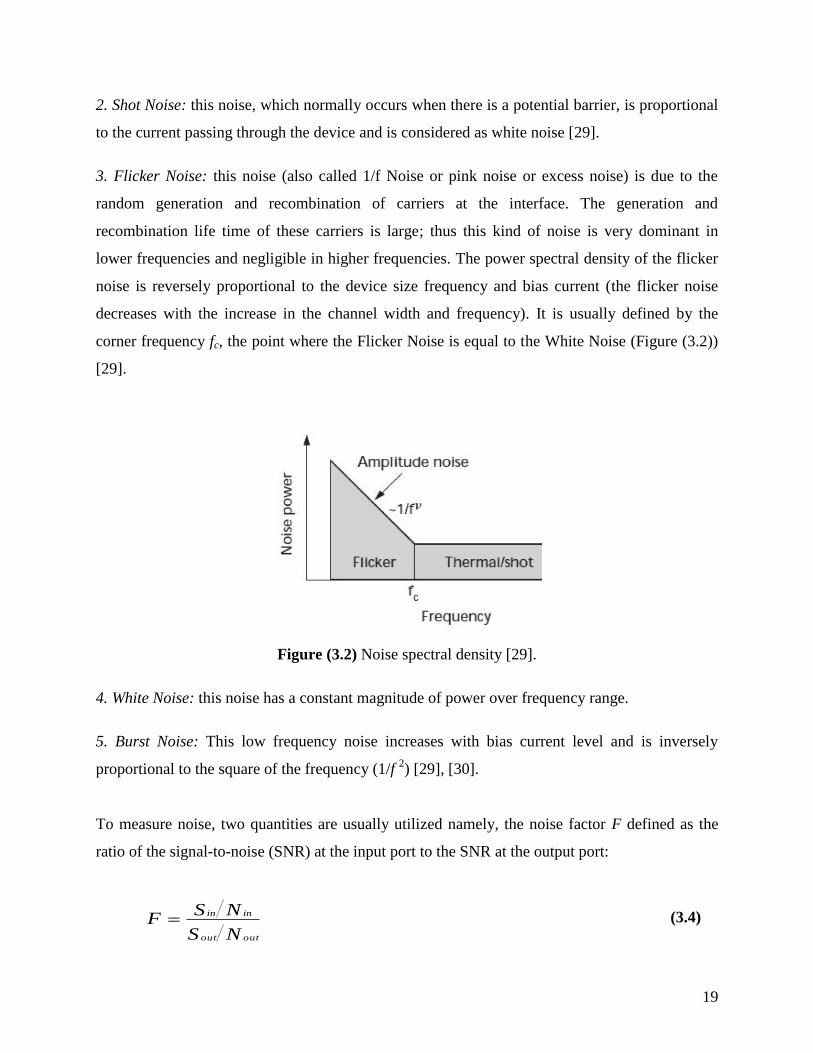
lower frequencies and negligible in higher frequencies. The power spectral density of the flicker
noise is reversely proportional to the device size frequency and bias current (the flicker noise
decreases with the increase in the channel width and frequency). It is usually defined by the
corner frequency fc, the point where the Flicker Noise is equal to the White Noise (Figure (3.2))
[29].
Figure (3.2) Noise spectral density [29].
4. White Noise: this noise has a constant magnitude of power over frequency range.
5. Burst Noise: This low frequency noise increases with bias current level and is inversely
proportional to the square of the frequency (1/f 2) [29], [30].
To measure noise, two quantities are usually utilized namely, the noise factor F defined as the
ratio of the signal-to-noise (SNR) at the input port to the SNR at the output port:
NS
NSF
outout
inin (3.4)
20
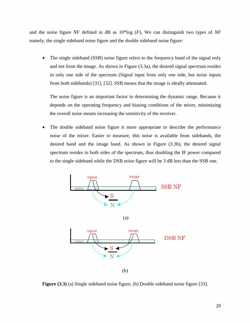
and the noise figure NF defined in dB as 10*log (F), We can distinguish two types of NF
namely, the single sideband noise figure and the double sideband noise figure:
The single sideband (SSB) noise figure refers to the frequency band of the signal only
and not from the image. As shown in Figure (3.3a), the desired signal spectrum resides
in only one side of the spectrum (Signal input from only one side, but noise inputs
from both sidebands) [31], [32]. SSB means that the image is ideally attenuated.
The noise figure is an important factor in determining the dynamic range. Because it
depends on the operating frequency and biasing conditions of the mixer, minimizing
the overall noise means increasing the sensitivity of the receiver.
The double sideband noise figure it more appropriate to describe the performance
noise of the mixer. Easier to measure, this noise is available from sidebands, the
desired band and the image band. As shown in Figure (3.3b), the desired signal
spectrum resides in both sides of the spectrum, thus doubling the IF power compared
to the single sideband while the DSB noise figure will be 3 dB less than the SSB one.
(a)
(b)
Figure (3.3) (a) Single sideband noise figure, (b) Double sideband noise figure [33].

21
3.2.3 Isolation
It quantifies the amount of signal leakage that may occur between two ports as reported in Figure
(3.4). Since the local oscillator is the most important signal, the isolations of the LO port vs. the
RF input port and the IF output port are critical parameters to consider. In fact, for some mixer
applications, the isolation should be as high as possible because the leakage to the input port can
remix with the input frequency (RF) and produce a (DC) offset Voltage, causing lost in the
information signal.
Figure (3.4) Leakage directions between the ports [34].
This LO leakage can also interfere with an incoming signal, therefore causing second harmonic
distortion, a serious problem in homodyne receivers. On the other side, if the leakage from the
LO port to the output IF port is large, this may degrade the performance of the next blocks,
causing processing errors and/or saturation.
The isolation is also a good indication of how the system is balanced. This effect will be the
same if the input (RF) or output (IF) frequency leaks to the local oscillator port. This effect can
be removed by either AC coupling or sub harmonic mixing [35].
3.2.4 Linearity
Any nonlinear transfer function can be described (approximated) mathematically by a power
series expansion such as a Taylor series expansion; the number of terms in the series determining
how strongly nonlinear is the function [36].
..........33
2210 VKVKVKKV inininout (3.5)
22
In this polynomial function the first term is a constant involving dc component, while the second
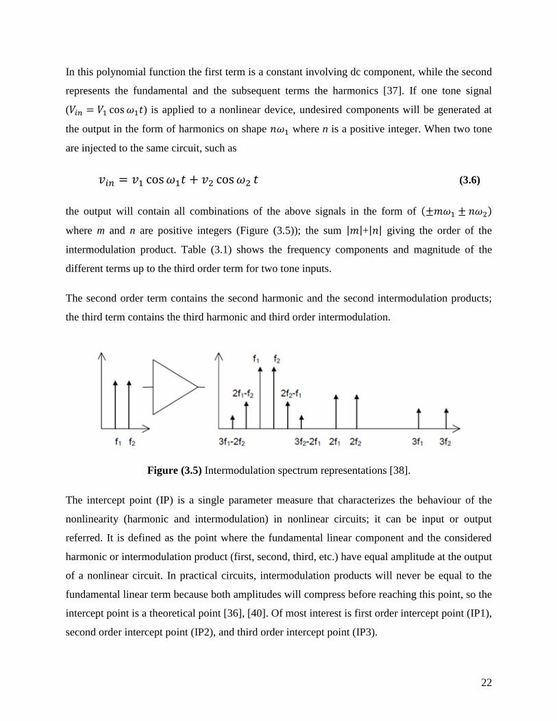
represents the fundamental and the subsequent terms the harmonics [37]. If one tone signal
( ) is applied to a nonlinear device, undesired components will be generated at
the output in the form of harmonics on shape where n is a positive integer. When two tone
are injected to the same circuit, such as
(3.6)
the output will contain all combinations of the above signals in the form of ( )
where m and n are positive integers (Figure (3.5)); the sum | |+| | giving the order of the
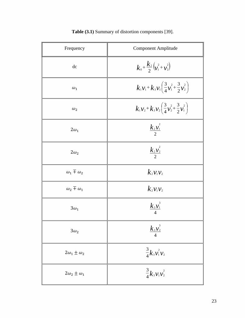
intermodulation product. Table (3.1) shows the frequency components and magnitude of the
different terms up to the third order term for two tone inputs.
The second order term contains the second harmonic and the second intermodulation products;
the third term contains the third harmonic and third order intermodulation.
Figure (3.5) Intermodulation spectrum representations [38].
The intercept point (IP) is a single parameter measure that characterizes the behaviour of the
nonlinearity (harmonic and intermodulation) in nonlinear circuits; it can be input or output
referred. It is defined as the point where the fundamental linear component and the considered
harmonic or intermodulation product (first, second, third, etc.) have equal amplitude at the output
of a nonlinear circuit. In practical circuits, intermodulation products will never be equal to the
fundamental linear term because both amplitudes will compress before reaching this point, so the
intercept point is a theoretical point [36], [40]. Of most interest is first order intercept point (IP1),
second order intercept point (IP2), and third order intercept point (IP3).
23
Table (3.1) Summary of distortion components [39].
Frequency Component Amplitude
dc vvk
k2
2
2
1
2
0 2
vvvkvk
2
2
2
11311 2
3
4
3
vvvkvk
2
1
2
22321 2
3
4
3
2
2
12vk
2
2
22vk
vvk 212
vvk 212
4
3
13vk
4
3
23vk
vvk 2
2
134
3
vvk2
2134
3
24
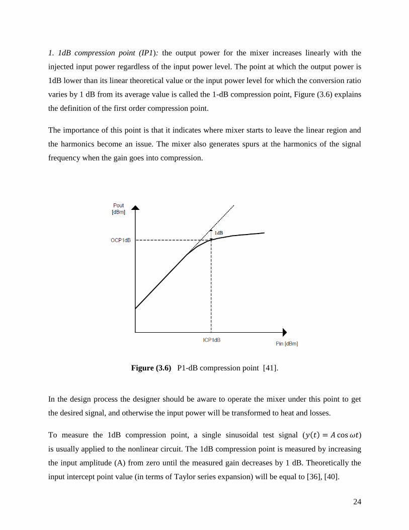
1. 1dB compression point (IP1): the output power for the mixer increases linearly with the
injected input power regardless of the input power level. The point at which the output power is
1dB lower than its linear theoretical value or the input power level for which the conversion ratio
varies by 1 dB from its average value is called the 1-dB compression point, Figure (3.6) explains
the definition of the first order compression point.
The importance of this point is that it indicates where mixer starts to leave the linear region and
the harmonics become an issue. The mixer also generates spurs at the harmonics of the signal
frequency when the gain goes into compression.
Figure (3.6) P1-dB compression point [41].
In the design process the designer should be aware to operate the mixer under this point to get
the desired signal, and otherwise the input power will be transformed to heat and losses.
To measure the 1dB compression point, a single sinusoidal test signal ( ( ) )
is usually applied to the nonlinear circuit. The 1dB compression point is measured by increasing
the input amplitude (A) from zero until the measured gain decreases by 1 dB. Theoretically the
input intercept point value (in terms of Taylor series expansion) will be equal to [36], [40].
25
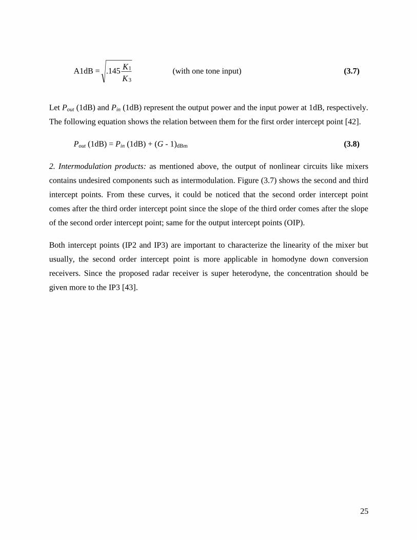
A1dB =K
K
3
1145. (with one tone input) (3.7)
Let Pout (1dB) and Pin (1dB) represent the output power and the input power at 1dB, respectively.
The following equation shows the relation between them for the first order intercept point [42].
Pout (1dB) = Pin (1dB) + (G - 1)dBm (3.8)
2. Intermodulation products: as mentioned above, the output of nonlinear circuits like mixers
contains undesired components such as intermodulation. Figure (3.7) shows the second and third
intercept points. From these curves, it could be noticed that the second order intercept point
comes after the third order intercept point since the slope of the third order comes after the slope
of the second order intercept point; same for the output intercept points (OIP).
Both intercept points (IP2 and IP3) are important to characterize the linearity of the mixer but
usually, the second order intercept point is more applicable in homodyne down conversion
receivers. Since the proposed radar receiver is super heterodyne, the concentration should be
given more to the IP3 [43].
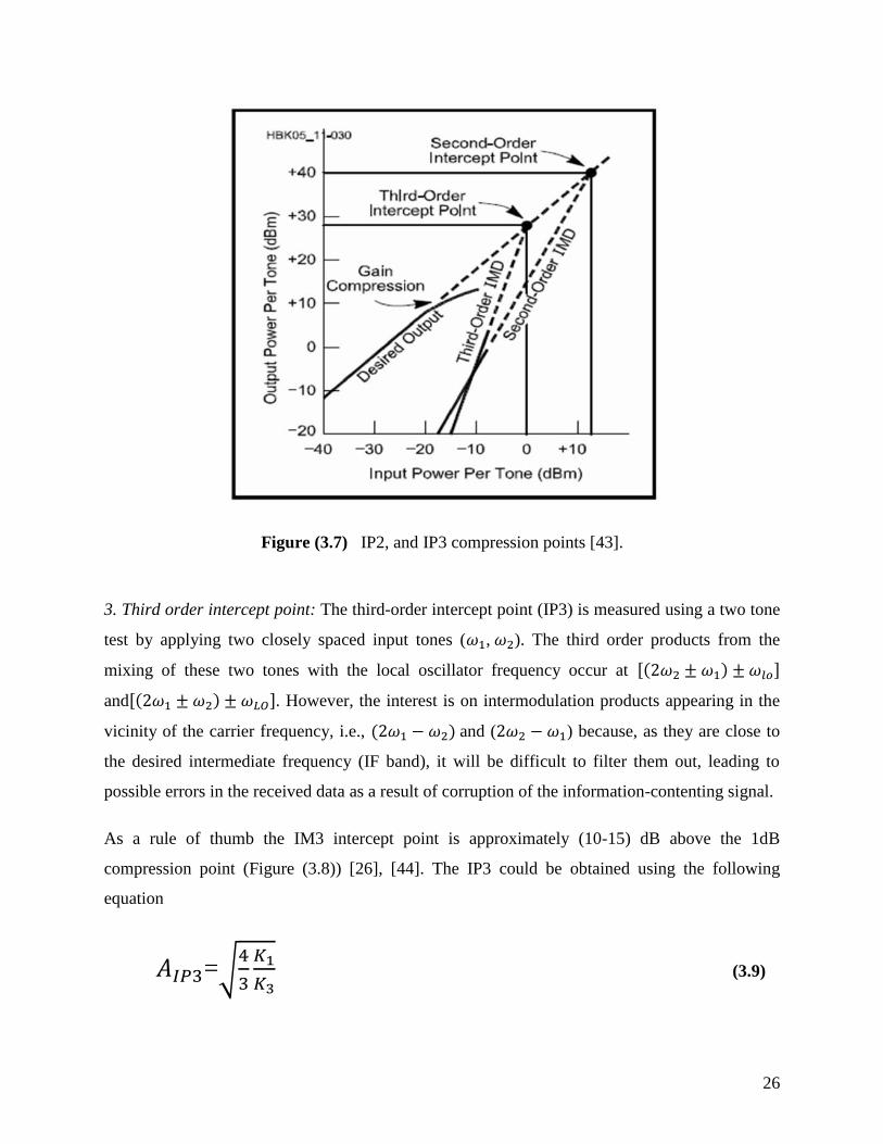
26
Figure (3.7) IP2, and IP3 compression points [43].
3. Third order intercept point: The third-order intercept point (IP3) is measured using a two tone
test by applying two closely spaced input tones ( , ). The third order products from the
mixing of these two tones with the local oscillator frequency occur at [( ) ]
and[( ) ]. However, the interest is on intermodulation products appearing in the
vicinity of the carrier frequency, i.e., ( ) and ( ) because, as they are close to
the desired intermediate frequency (IF band), it will be difficult to filter them out, leading to
possible errors in the received data as a result of corruption of the information-contenting signal.
As a rule of thumb the IM3 intercept point is approximately (10-15) dB above the 1dB
compression point (Figure (3.8)) [26], [44]. The IP3 could be obtained using the following
equation
=√
(3.9)
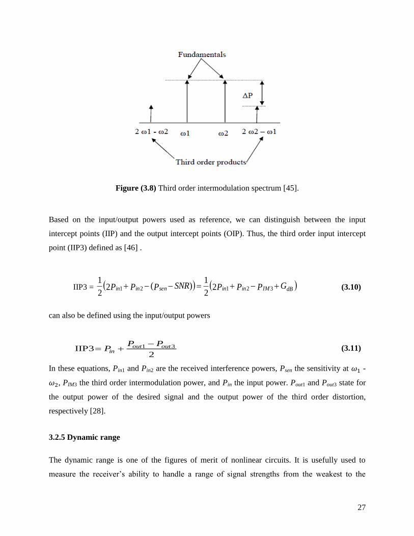
27
Figure (3.8) Third order intermodulation spectrum [45].
Based on the input/output powers used as reference, we can distinguish between the input
intercept points (IIP) and the output intercept points (OIP). Thus, the third order input intercept
point (IIP3) defined as [46] .
IIP3 = dBIMininseninin GPPPSNRPPP 32121 22
1)(2
2
1 (3.10)
can also be defined using the input/output powers
2IIP3 31 outout
in
PPP
(3.11)
In these equations, Pin1 and Pin2 are the received interference powers, Psen the sensitivity at -
, PIM3 the third order intermodulation power, and Pin the input power. Pout1 and Pout3 state for
the output power of the desired signal and the output power of the third order distortion,
respectively [28].
3.2.5 Dynamic range
The dynamic range is one of the figures of merit of nonlinear circuits. It is usefully used to
measure the receiver’s ability to handle a range of signal strengths from the weakest to the
28
strongest. It also shows the capability of the receiver to detect weak signals in the presence of
large-amplitude signals.
The dynamic range could be defined either as the ratio of the smallest usable signal to the largest
tolerable signal or the amplitude range over which a mixer can operate without degradation of
performance.
The lower limit of the dynamic range is the receiver noise floor set by the receiver sensitivity,
i.e., the lowest input signal power that the receiver can successfully process (or the minimum
signal strength that can be detected).
The receiver sensitivity can be measured by the minimum detectable signal (MDS) which is
related to the receiver noise and the system bandwidth. The minimum detectable signal is the
smallest signal power that can be received or the smallest signal that can be detected above
noise, and it determines the minimum signal-to-noise ratio at the output of the receiver (SNRout).
Larger negative numbers are generally better but, at the same time, too much sensitivity can
reduce strong signal dynamic range and IIP3 [30], [47]-[49].
The minimum detectable signal can be calculated using the following equation
dBoutdBdBmin SNRNFBP log10174min, (3.12)
Where -174 represents the noise power (in dBm) and NF the noise figure for the receiver. SNRout
is the minimum signal-to-noise power ratio at the output [50].
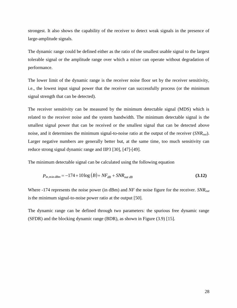
The dynamic range can be defined through two parameters: the spurious free dynamic range
(SFDR) and the blocking dynamic range (BDR), as shown in Figure (3.9) [15].

29
Figure (3.9) Dynamic range [51].
The spurious free dynamic range (SFDR) is a commonly used figure of merit to describe
the dynamic range of an RF system. It could be defined as the input signal range from the
intercept of noise floor and fundamental signal power to the intercept of noise floor and the
3rd
order intermodulation distortion power. It could be also defined as the input range from
the minimum detectable signal to the maximum undistorted signal [28] [52]-[54]:
MDSGIPSNRFloorNoiseIIPSFDR 33
23
3
2min (3.13)
where is the minimum detectable signal, IP3 the third order intercept point, G the
gain in dB and MDS the minimum detectable signal.
The blocking dynamic range (BDR) shows when the receiver's sensitivity begins to drop in
the presence of strong nearby signals. It could be then defined as the input power range
from the intercept of noise floor and fundamental signal power to the input 1-dB
compression point. It is often used to measure a receiver's ability to tolerate a strong signal
without losing its sensitivity [55]-[57].
30
3.3 Mixer topologies
Mixers can be classified into passive mixers and active mixers.
3.3.1 Passive mixers
This type of mixer exhibits losses instead of gain, so there is no amplification for the input
signal. However, it is widely used because of its relatively low cost, simplicity in the design,
high bandwidth, and high linearity [58], [59]. Also, it needs high local oscillator power which is
considered as one of the main disadvantages for this type of mixers.
Passive mixing can be obtained using passive switches driven by the local oscillator frequency.
By this way, the multiplication is realized by each switch commutating the input radio frequency
signal: the switch is turn on when the LO signal is above a certain voltage, and the mixing
process could be expressed mathematically by multiplying the RF frequency with a square wave,
this square wave being the LO signal.
In practice, such mixers are made of nonlinear diodes or FETs; diode mixers having important
advantage over FET mixers because of their wider bandwidth (FET mixers exhibit high-Q gate-
input impedance that cause difficulties in achieving flat wide bandwidth).
Passive mixers in general exhibit better noise performance and lower distortion but very low port
isolation [24], [47].
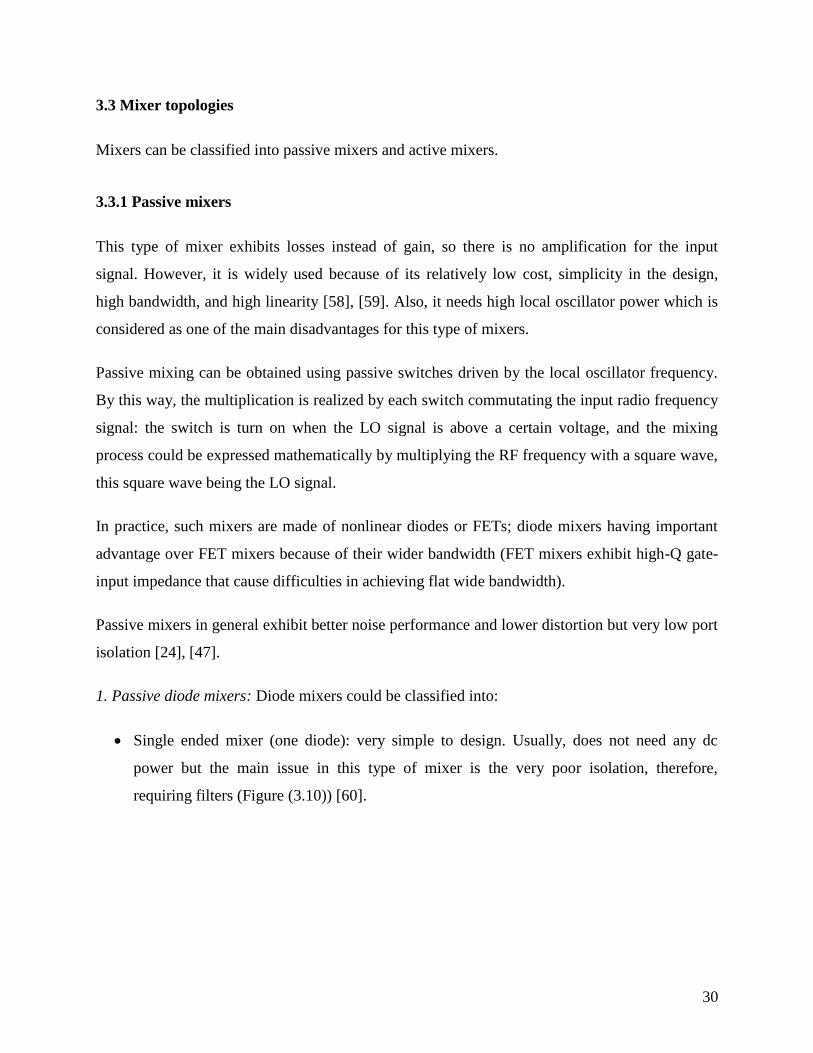
1. Passive diode mixers: Diode mixers could be classified into:
Single ended mixer (one diode): very simple to design. Usually, does not need any dc
power but the main issue in this type of mixer is the very poor isolation, therefore,
requiring filters (Figure (3.10)) [60].
31
Figure (3.10) Single diode mixer [60].
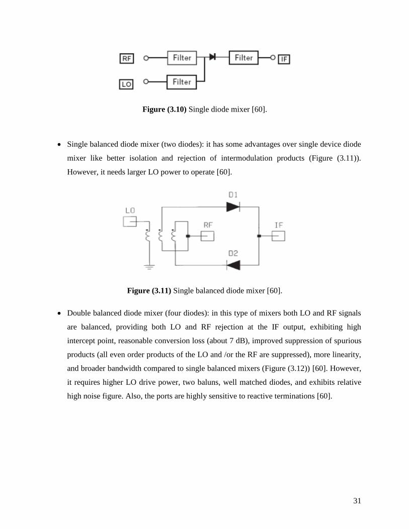
Single balanced diode mixer (two diodes): it has some advantages over single device diode
mixer like better isolation and rejection of intermodulation products (Figure (3.11)).
However, it needs larger LO power to operate [60].
Figure (3.11) Single balanced diode mixer [60].
Double balanced diode mixer (four diodes): in this type of mixers both LO and RF signals
are balanced, providing both LO and RF rejection at the IF output, exhibiting high
intercept point, reasonable conversion loss (about 7 dB), improved suppression of spurious
products (all even order products of the LO and /or the RF are suppressed), more linearity,
and broader bandwidth compared to single balanced mixers (Figure (3.12)) [60]. However,
it requires higher LO drive power, two baluns, well matched diodes, and exhibits relative
high noise figure. Also, the ports are highly sensitive to reactive terminations [60].

32
Figure (3.12) Double balance mixer [60].
2. Passive FET mixers: FET resistive mixers use the resistive channel of a FET to provide low-
distortion mixing with the similar conversion loss as diode mixers. Also, it exists single ended
FET mixer, single balanced and double balanced FET mixers as shown in Figure (3.13) [60].
Compared to diode mixers, FET mixers have better P-1dB compression point performance.
Figure (3.13) FET Resistive Mixer [60].
33
3.3.2 Active mixers
These transistor mixers can provide gain from RF to IF signals, which, in turn, reduces the noise
contributions of the mixer and succeeding receiver stages. However, it is more difficult to
achieve good linearity, i.e., to obtain high third-order intercepts and 1-dB compression points [5].
As for passive mixers, active mixers can be classified as:
1. Active single device mixers: they use the LO signal to vary the transconductance of the
transistor. Among such mixers, we have:
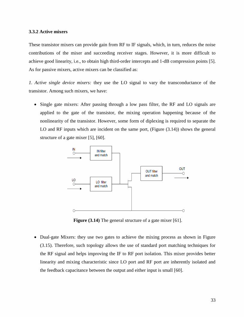
Single gate mixers: After passing through a low pass filter, the RF and LO signals are
applied to the gate of the transistor, the mixing operation happening because of the
nonlinearity of the transistor. However, some form of diplexing is required to separate the
LO and RF inputs which are incident on the same port, (Figure (3.14)) shows the general
structure of a gate mixer [5], [60].
Figure (3.14) The general structure of a gate mixer [61].
Dual-gate Mixers: they use two gates to achieve the mixing process as shown in Figure
(3.15). Therefore, such topology allows the use of standard port matching techniques for
the RF signal and helps improving the IF to RF port isolation. This mixer provides better
linearity and mixing characteristic since LO port and RF port are inherently isolated and
the feedback capacitance between the output and either input is small [60].
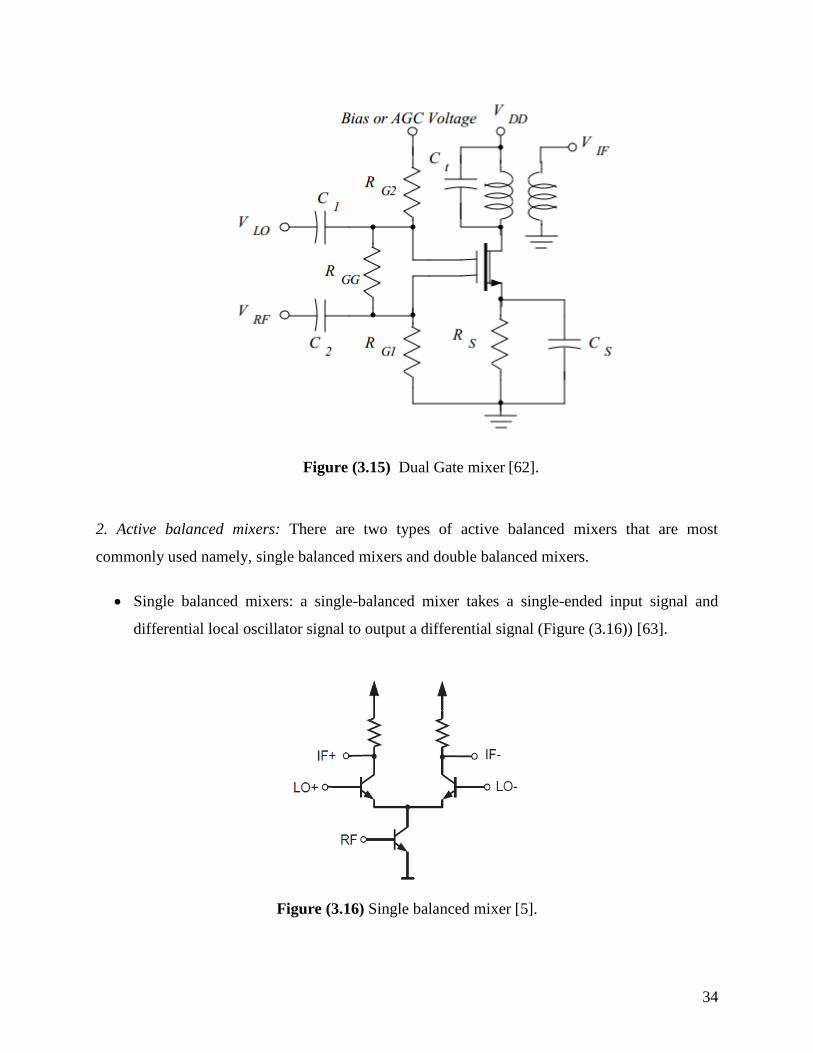
34
Figure (3.15) Dual Gate mixer [62].
2. Active balanced mixers: There are two types of active balanced mixers that are most
commonly used namely, single balanced mixers and double balanced mixers.
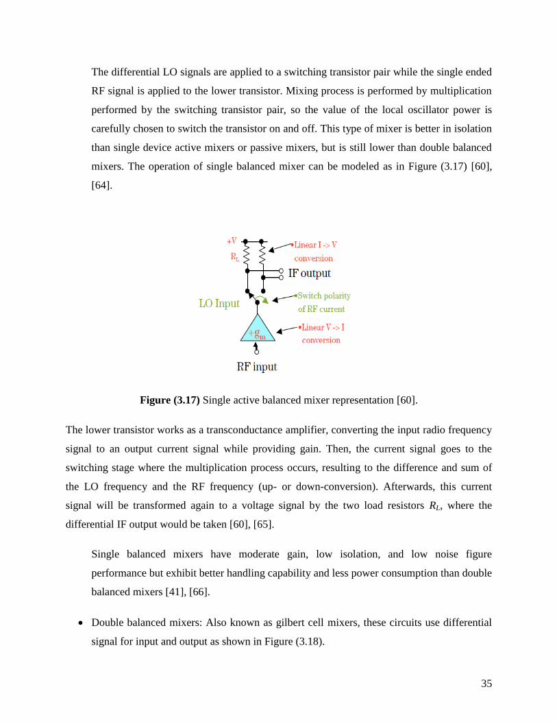
Single balanced mixers: a single-balanced mixer takes a single-ended input signal and
differential local oscillator signal to output a differential signal (Figure (3.16)) [63].
Figure (3.16) Single balanced mixer [5].
35
The differential LO signals are applied to a switching transistor pair while the single ended
RF signal is applied to the lower transistor. Mixing process is performed by multiplication
performed by the switching transistor pair, so the value of the local oscillator power is
carefully chosen to switch the transistor on and off. This type of mixer is better in isolation
than single device active mixers or passive mixers, but is still lower than double balanced
mixers. The operation of single balanced mixer can be modeled as in Figure (3.17) [60],
[64].
Figure (3.17) Single active balanced mixer representation [60].
The lower transistor works as a transconductance amplifier, converting the input radio frequency
signal to an output current signal while providing gain. Then, the current signal goes to the
switching stage where the multiplication process occurs, resulting to the difference and sum of
the LO frequency and the RF frequency (up- or down-conversion). Afterwards, this current
signal will be transformed again to a voltage signal by the two load resistors RL, where the
differential IF output would be taken [60], [65].
Single balanced mixers have moderate gain, low isolation, and low noise figure
performance but exhibit better handling capability and less power consumption than double
balanced mixers [41], [66].
Double balanced mixers: Also known as gilbert cell mixers, these circuits use differential
signal for input and output as shown in Figure (3.18).
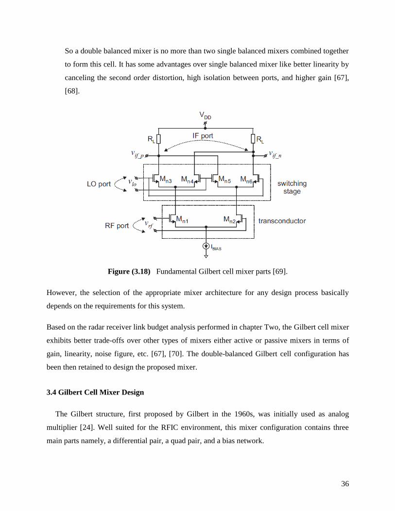
36
So a double balanced mixer is no more than two single balanced mixers combined together
to form this cell. It has some advantages over single balanced mixer like better linearity by
canceling the second order distortion, high isolation between ports, and higher gain [67],
[68].
Figure (3.18) Fundamental Gilbert cell mixer parts [69].
However, the selection of the appropriate mixer architecture for any design process basically
depends on the requirements for this system.
Based on the radar receiver link budget analysis performed in chapter Two, the Gilbert cell mixer
exhibits better trade-offs over other types of mixers either active or passive mixers in terms of
gain, linearity, noise figure, etc. [67], [70]. The double-balanced Gilbert cell configuration has
been then retained to design the proposed mixer.
3.4 Gilbert Cell Mixer Design
The Gilbert structure, first proposed by Gilbert in the 1960s, was initially used as analog
multiplier [24]. Well suited for the RFIC environment, this mixer configuration contains three
main parts namely, a differential pair, a quad pair, and a bias network.
37
By taking advantage of this differential pair (considered as differential amplifier), the Gilbert cell
can fix feed through issues and provide high port-to-port isolations as well as high gain and low
noise figure. Indeed, because LO and RF stages are balanced, this circuit shows high LO and RF
rejection at the IF output (all the ports being inherently isolated from each other), increased
linearity resulting on high intercept points, improved suppression of spurious (all even products
of LO and RF frequencies being suppressed) [71]-[73].
At the same time there are some disadvantages for the Gilbert cell mixer mainly because it
requires a high LO drive level and three baluns. Also, the ports are highly sensitive to reactive
terminations, any small phase mismatch between the LO+ and LO- can lead to significant local
oscillator leakage. Furthermore, the Gilbert cell is not suitable for low voltage applications [74]-
[76].
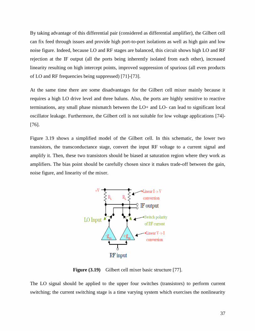
Figure 3.19 shows a simplified model of the Gilbert cell. In this schematic, the lower two
transistors, the transconductance stage, convert the input RF voltage to a current signal and
amplify it. Then, these two transistors should be biased at saturation region where they work as
amplifiers. The bias point should be carefully chosen since it makes trade-off between the gain,
noise figure, and linearity of the mixer.
Figure (3.19) Gilbert cell mixer basic structure [77].
The LO signal should be applied to the upper four switches (transistors) to perform current
switching; the current switching stage is a time varying system which exercises the nonlinearity
38
property to perform mixing operation. These four transistors should be biased in the deep triode
region (around pinch-off region) and the LO signal voltage should be high enough to perform
valid switching and to switch the RF current from one side to the other side of the differential
output pairs [28], [78]-[81].
Now suppose the input RF signal is ( ). This voltage is amplified and
transformed to a current signal gm by the differential pair, with gm the transconductance. This
current signal goes to the upper quad transistors along with the LO input signal which function as
a switch to perform current switching. In fact, the LO input signal is a kind of square wave signal
whose amplitude is between -1 and 1 and frequency fLO, therefore, generating odd harmonics and
leading to
(3.14)
Now the harmonic terms could be filtered out and the result will be transformed to a voltage
signal by using the two load resistors RL, thus giving,
(3.15)
To calculate the desired voltage gain for a down conversion mixer, the up conversion term
should be filtered out and by dividing the output voltage over the input voltage the following
expressions can be deduced [82].
(3.16)

39
3.5 Conclusion
In this chapter, the mixing theory as well as the different mixer configurations and properties
have been introduced and discussed. The preference has been given to Gilbert cell mixers for
radar applications because of their advantages over other types of mixers like higher gain, higher
linearity, higher isolation, etc. However they require two baluns to convert the single RF and LO
input signals to differential pairs as well as a combiner to combine the output differential signals
into a single signal. Therefore, three 3dB 180o baluns should be built. This will be the purpose of
the next chapter.
40
Chapter 4
Coupler Design
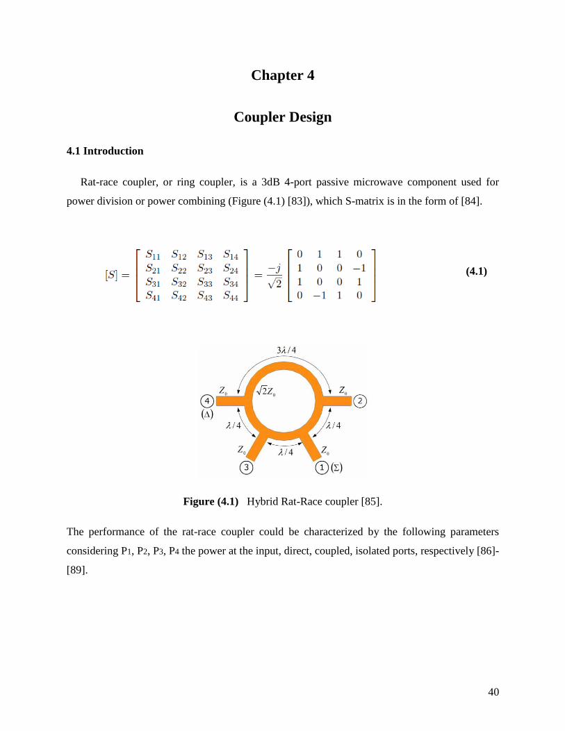
4.1 Introduction
Rat-race coupler, or ring coupler, is a 3dB 4-port passive microwave component used for
power division or power combining (Figure (4.1) [83]), which S-matrix is in the form of [84].
(4.1)
Figure (4.1) Hybrid Rat-Race coupler [85].
The performance of the rat-race coupler could be characterized by the following parameters
considering P1, P2, P3, P4 the power at the input, direct, coupled, isolated ports, respectively [86]-
[89].

41
Coupling (K): the level of the input power that is coupled to the output port or the Ratio
between the power at the input port to the power at the coupled port
dBK SP
P ,log20log10 13
3
1 (4.2)
Directivity (D): shows the input power transferred to the coupled port without reflection
dBDS
S
P
P ,log20log1014
13
4
3
(4.3)
Through (G): the level of the input power transferred to the direct port or the ratio between
the input signal power and the output power at the direct port
dBG SP
P ,log20log10 12
2
1 (4.4)
Isolation (I): the amount of the input power that exist at the isolation port or the ability of
the coupler to prevent the input signal to travel toward the isolated port
dBI SP
P ,log20log10 14
4
1 (4.5)
Return losses (RL): measures the input impedance matching or the level of power that is
reflected from the input port
dBRL S ,log20 11 (4.6)
The other parameters are the amplitude imbalance, i.e., the difference in the amplitude power
between the two signals at the output ports, and the phase imbalance, i.e., the difference in the
42
phase between the two outputs ports signals phases. An amplitude imbalance of 1dB and a phase
difference less than 5o are generally accepted [90].
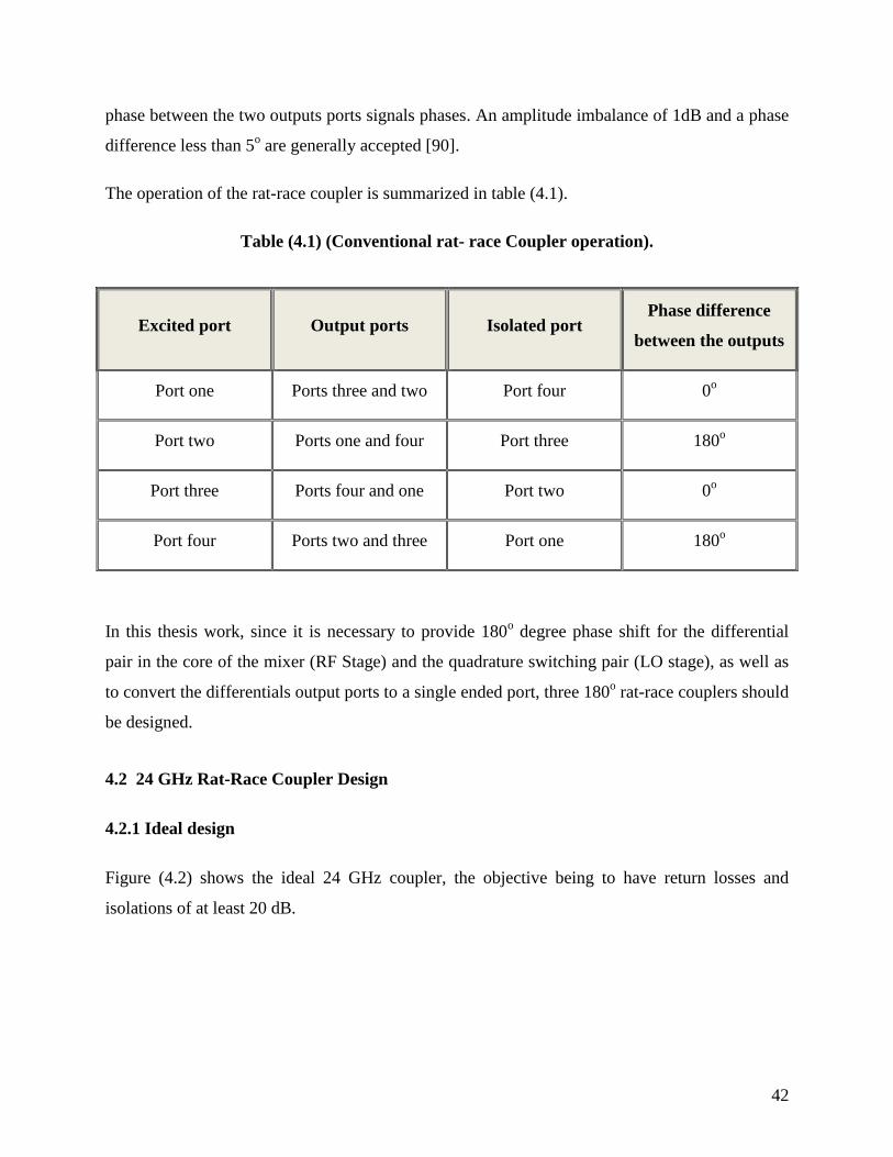
The operation of the rat-race coupler is summarized in table (4.1).
Table (4.1) (Conventional rat- race Coupler operation).
Excited port Output ports Isolated port Phase difference
between the outputs
Port one Ports three and two Port four 0o
Port two Ports one and four Port three 180o
Port three Ports four and one Port two 0o
Port four Ports two and three Port one 180o
In this thesis work, since it is necessary to provide 180o degree phase shift for the differential
pair in the core of the mixer (RF Stage) and the quadrature switching pair (LO stage), as well as
to convert the differentials output ports to a single ended port, three 180o rat-race couplers should
be designed.
4.2 24 GHz Rat-Race Coupler Design
4.2.1 Ideal design
Figure (4.2) shows the ideal 24 GHz coupler, the objective being to have return losses and
isolations of at least 20 dB.

43
Figure (4.2) Ideal 24 GHz rat-race coupler schematic.
Figures (4.3) to (4.6) show the coupler performance in terms of coupling, return loss, isolation
and imbalance.
4.2.2 Layout design
A substrate with a relative permittivity of 12.9, a height of 100 μm, a conductor thickness of
1μm, and a dielectric loss tangent of 0.001 has been used to design the coupler through
transmission line models from the pHEMT GaAs package provided by Win Semiconductor
Corporation (Figure (4.7), leading to the layout shown in Figure (4.8).
44
Figure (4.3) Simulated coupling.
Figure (4.4) Simulated amplitude imbalance.
Figure (4.5) Simulated isolation and input return loss.
Figure (4.6) Simulated phase imbalance.
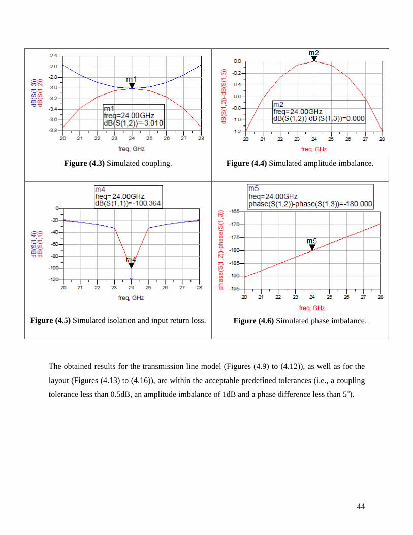
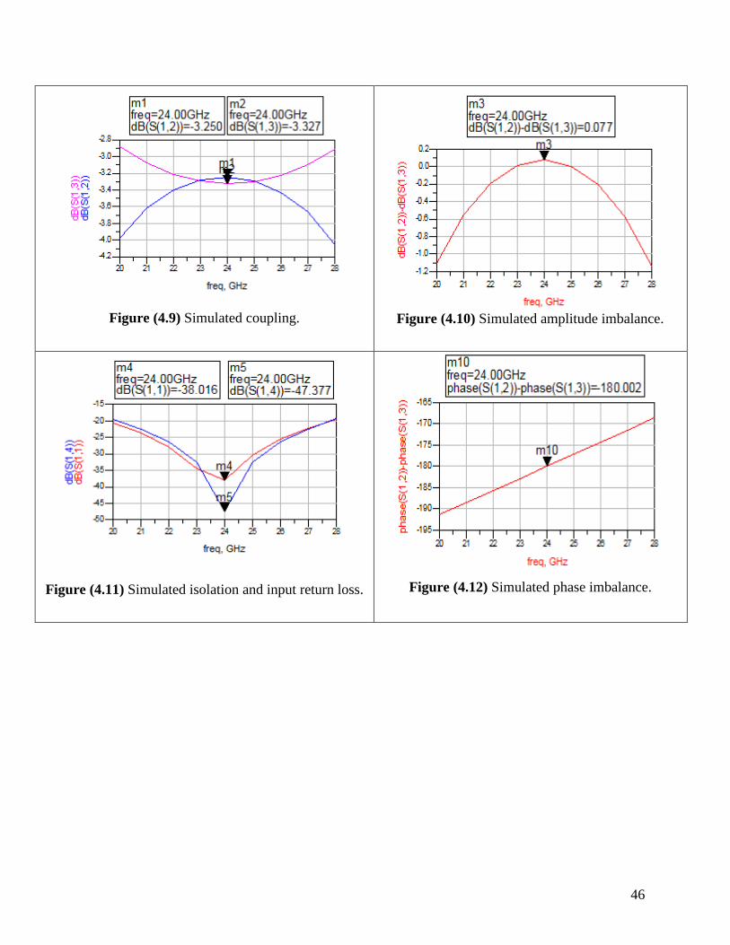
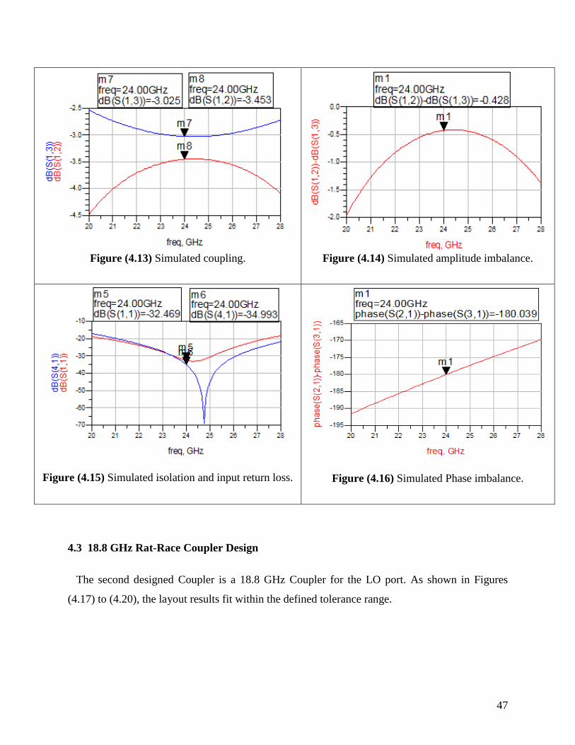
The obtained results for the transmission line model (Figures (4.9) to (4.12)), as well as for the
layout (Figures (4.13) to (4.16)), are within the acceptable predefined tolerances (i.e., a coupling
tolerance less than 0.5dB, an amplitude imbalance of 1dB and a phase difference less than 5o).

45
Figure (4.7) 24 GHz rat- race coupler: transmission line schematic.
Figure (4.8) 24 GHz rat- race coupler layout.
46
Figure (4.9) Simulated coupling.
Figure (4.10) Simulated amplitude imbalance.
Figure (4.11) Simulated isolation and input return loss.
Figure (4.12) Simulated phase imbalance.
47
Figure (4.13) Simulated coupling.
Figure (4.14) Simulated amplitude imbalance.
Figure (4.15) Simulated isolation and input return loss.
Figure (4.16) Simulated Phase imbalance.
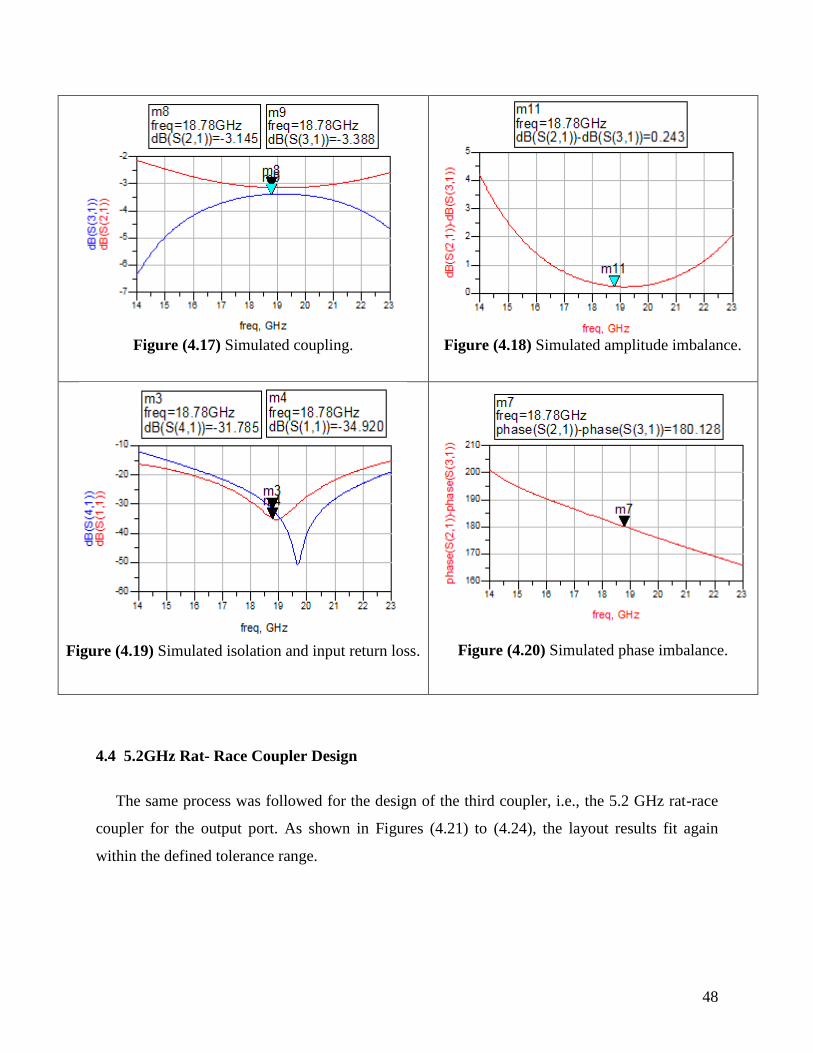
4.3 18.8 GHz Rat-Race Coupler Design
The second designed Coupler is a 18.8 GHz Coupler for the LO port. As shown in Figures
(4.17) to (4.20), the layout results fit within the defined tolerance range.
48
Figure (4.17) Simulated coupling.
Figure (4.18) Simulated amplitude imbalance.
Figure (4.19) Simulated isolation and input return loss.
Figure (4.20) Simulated phase imbalance.
4.4 5.2GHz Rat- Race Coupler Design
The same process was followed for the design of the third coupler, i.e., the 5.2 GHz rat-race
coupler for the output port. As shown in Figures (4.21) to (4.24), the layout results fit again
within the defined tolerance range.
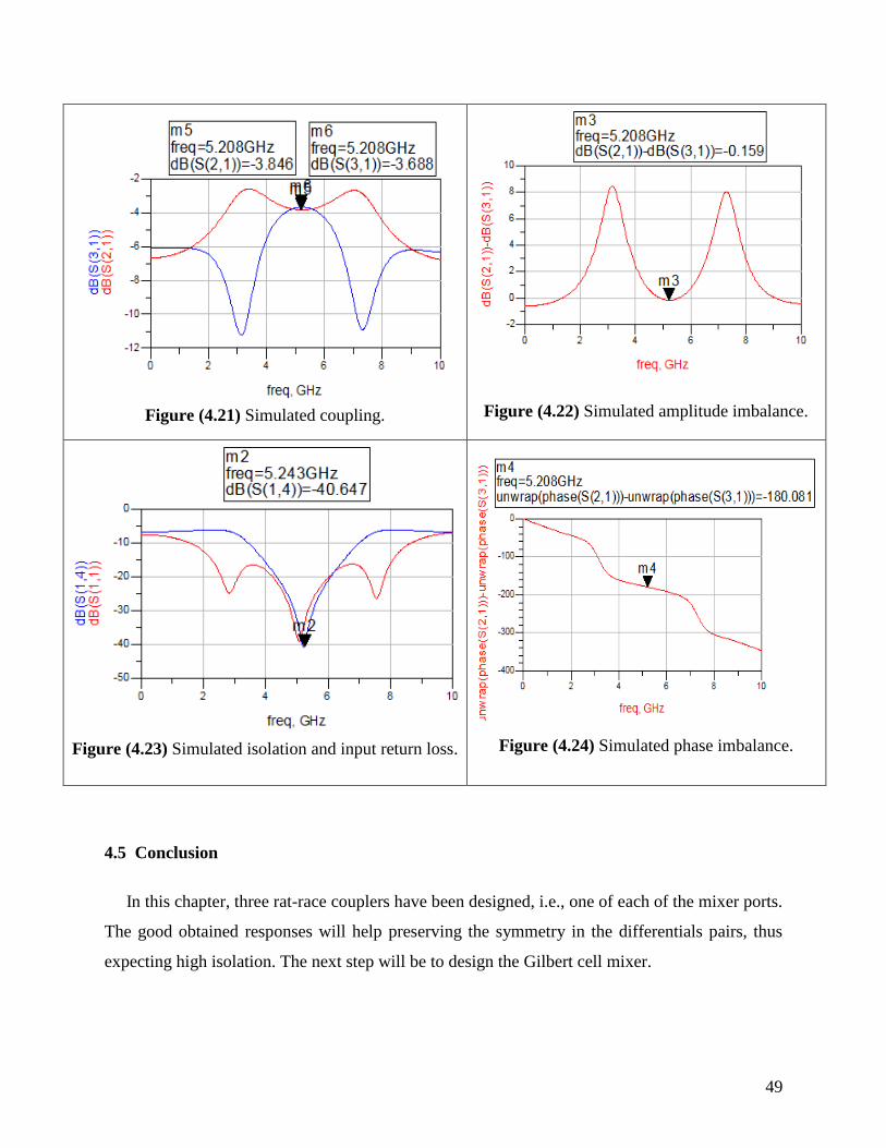
49
Figure (4.21) Simulated coupling.
Figure (4.22) Simulated amplitude imbalance.
Figure (4.23) Simulated isolation and input return loss.
Figure (4.24) Simulated phase imbalance.
4.5 Conclusion
In this chapter, three rat-race couplers have been designed, i.e., one of each of the mixer ports.
The good obtained responses will help preserving the symmetry in the differentials pairs, thus
expecting high isolation. The next step will be to design the Gilbert cell mixer.

50
Chapter 5
Mixer Design
The mixer to design should meet certain requirements as detailed in Chapter 2. They are
summarized in Table (5.1) for reader convenience.
Table (5.1) Gilbert Cell Mixer Specifications.
Parameters Values
RF Frequency 24 GHz
LO Frequency 18.8 GHz
IF Frequency 5.2 GHz
Minimum Conversion Gain 8.3 dB
Maximum NF 10.5 dB
Minimum P1dB -18 dBm
Minimum IIP3 -8 dBm
Minimum Leakage 20 dB
Minimum S11 and S22 -10 dB
51
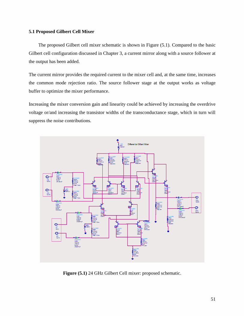
5.1 Proposed Gilbert Cell Mixer
The proposed Gilbert cell mixer schematic is shown in Figure (5.1). Compared to the basic
Gilbert cell configuration discussed in Chapter 3, a current mirror along with a source follower at
the output has been added.
The current mirror provides the required current to the mixer cell and, at the same time, increases
the common mode rejection ratio. The source follower stage at the output works as voltage
buffer to optimize the mixer performance.
Increasing the mixer conversion gain and linearity could be achieved by increasing the overdrive
voltage or/and increasing the transistor widths of the transconductance stage, which in turn will
suppress the noise contributions.
Figure (5.1) 24 GHz Gilbert Cell mixer: proposed schematic.

52
However, increasing the current through the transconductance stage will increase the current
through the switching stage and load resistors, causing some drawbacks like increasing the
thermal noise and the voltage drop across these resistors; so voltage head room issues could
appear and the output voltage signal may clip.
Also, increasing the current through the switching stage will increase the noise figure, thus
requiring larger sizes for the transistors to handle the extra current in the switching pairs, leading
to more switching time. In fact, increasing the width of the switching transistors increases the
device capacitance. Thus, the unity gain frequency ft, which is responsible for the switching
speed, will be reduced and the switching process will be slower [91]-[94].
Moreover, increasing the size of the switching transistors needs more LO drive power to
complete the switching process, therefore, more dc power [95, 96]. Because of these drawbacks
in increasing the current through the load resistors and switching stages, a current bleeding
technique can be used to increase the current through the transconductance stage only without
increasing the currents through the load resistors or the switching stages [97].
This technique is shown in Figure (5.2); it has two current sources connected at the drain of the
switching stages and considered as part of the input stage. So the current flowing at the quad
switching stages is the difference between the currents in the differential pair and the currents
provided by the currents sources [98]; by this way, the current will be higher in the
transconductance stage, while the current through the load resistors and switching stage could be
reduced .
Therefore, this technique has been used in the present work to improve the design. In Figure
(5.1), this stage is represented by the two resistors connected from the main voltage source to the
drain of the transconductance stages.

53
Figure (5.2) Current bleeding technique [98].
5.2 Transistor Sizing
The Gilbert cell mixer design process can be sequenced through different steps, the first being
to adequately size the different transistors
5.2.1 Transistor sizing for the RF-LO stages
The transistor sizing for the RF and LO stages is a trade-off between mixer gain, noise figure,
linearity, power consumption, and unity current gain frequency.
In this design, the transistors of the RF stage were sized so that the current passing through them
ensures minimum noise figure. As shown in Figure (5.3), the required current for minimum noise
figure is around 6.7 mA for each single transistor of the differential pair, leading to a width of
(4*25µm). This relatively small width is desired because a small current achieving a high gm
means low power consumption. Also, losses and leakage through the capacitive substrate will be
reduced as well [99].

54
Figure (5.3) Simulated minimum noise figure over drain current.
For the LO switching stage, the transistors should be sized to work close to their ft to ensure
complete and fast switching [26]. For that reason, the width is kept the same as for the RF stage
(4*25µm). Under these conditions, the ft is larger than 200 GHz, i.e., sufficiently large for the
present design (Figure (5.4)).
Figure (5.4) Simulated unity current gain frequency (ft).

55
5.2.2 Transistor sizing for the source follower stage
As mentioned above, the common drain is used as a buffer voltage, i.e., high input impedance
and low output impedance and high output current [78], [100]. So choosing large widths (i.e.,
large gm) will lead to low output; the widths of the source follower stages transistors were then
assigned to (6*100) µm, large enough to minimize the loss at the output and to work as voltage
buffer.
5.2.3 Transistor sizing for the current mirror
To ensure a current of 6.7 mA in the differential pair, the current passing through the current
mirror transistor should be around 13.4 mA. So the width of the current mirror transistor was
chosen as (4*40) µm.
5.3 DC Analysis
After sizing the transistor, the following step is to adequately bias these transistors. As
mentioned above, the two transistors of the differential pair should be biased in the saturation
region to work as amplifiers. Figure (5.5) shows that the threshold voltage for this transistor is
around -0.7V; thus, a VGS voltage of -0.3V, Figure (5.6) shows that the current is, as expected,
about 6.7 mA.
The LO switching transistor pair should be biased according to Figure (5.7), with VGS = -0.45V,
VDS = 0.7V and a current ID of about 2mA, i.e., enough to keep the transistor working beside the
pinch off region for better switching efficiency while providing enough voltage headroom at the
output without clipping at higher input signals.
Two resistors of 10 Ω have been included in the current mirror configuration (Figure (5.8)) for
thermal stability and to provide the desired bias point as in Figure (5.9), i.e., a current of about
15mA, which leads to a drain resistor of 172 Ω and a current bleeding resistor of 500 Ω.
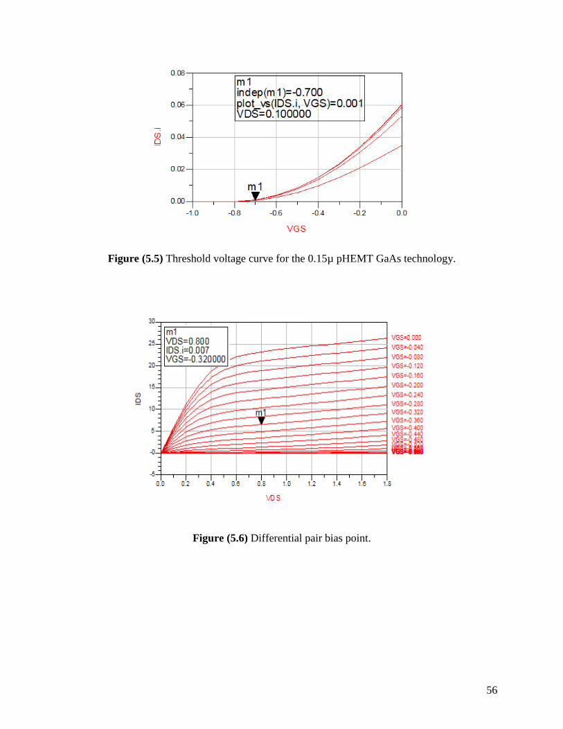
56
Figure (5.5) Threshold voltage curve for the 0.15µ pHEMT GaAs technology.
Figure (5.6) Differential pair bias point.

57
Figure (5.7) Switching stage transistor bias point.
The last block to bias was the output buffer. The values of the two resistors at the source of these
transistors were tuned for best output gain, leading to the bias point shown in Figure (5.10).
Figure (5.8) Depletion mode current mirror.
To the input of the
differential pair
To the main
voltage source
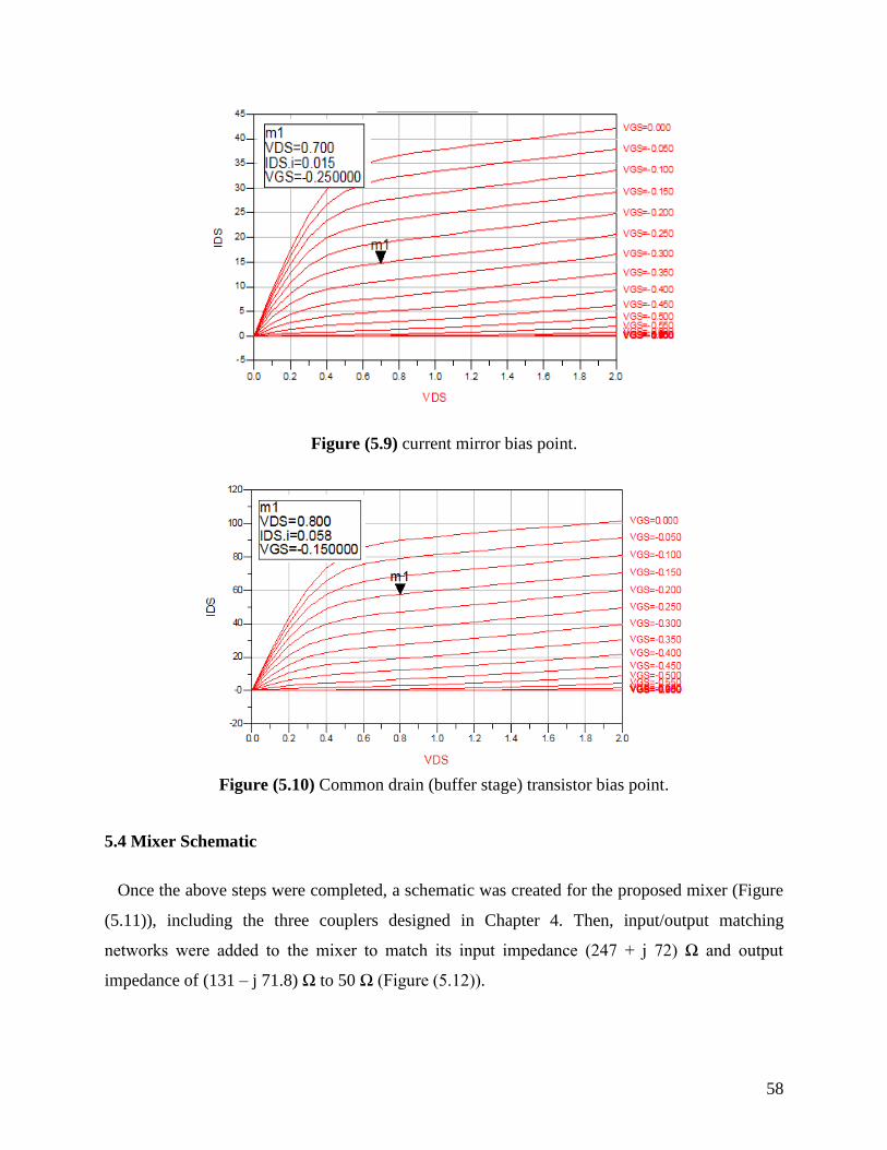
58
Figure (5.9) current mirror bias point.
Figure (5.10) Common drain (buffer stage) transistor bias point.
5.4 Mixer Schematic
Once the above steps were completed, a schematic was created for the proposed mixer (Figure
(5.11)), including the three couplers designed in Chapter 4. Then, input/output matching
networks were added to the mixer to match its input impedance (247 + j 72) Ω and output
impedance of (131 – j 71.8) Ω to 50 Ω (Figure (5.12)).
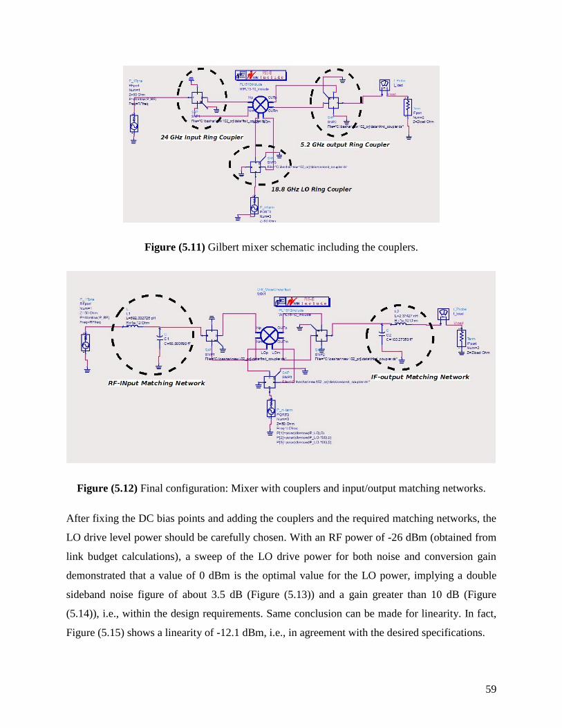
59
Figure (5.11) Gilbert mixer schematic including the couplers.
Figure (5.12) Final configuration: Mixer with couplers and input/output matching networks.
After fixing the DC bias points and adding the couplers and the required matching networks, the
LO drive level power should be carefully chosen. With an RF power of -26 dBm (obtained from
link budget calculations), a sweep of the LO drive power for both noise and conversion gain
demonstrated that a value of 0 dBm is the optimal value for the LO power, implying a double
sideband noise figure of about 3.5 dB (Figure (5.13)) and a gain greater than 10 dB (Figure
(5.14)), i.e., within the design requirements. Same conclusion can be made for linearity. In fact,
Figure (5.15) shows a linearity of -12.1 dBm, i.e., in agreement with the desired specifications.

60
Figures (5.16) and (5.17) show that this LO power level gives an optimum respective noise
figure and gain over the operating bandwidth. Further simulations demonstrated that the
designed mixer exhibits high isolation between ports (e.g., -72dB between the LO-RF ports, as
shown in Figure (5.18)). Note that the mixer input/output spectrums (Figure (5.19)) and
input/output return losses (Figure (5.20)) further confirmed the efficiency of the proposed design.
Figure (5.13) Simulated SSB noise figure versus LO power.
Figure (5.14) Simulated conversion gain versus LO power.
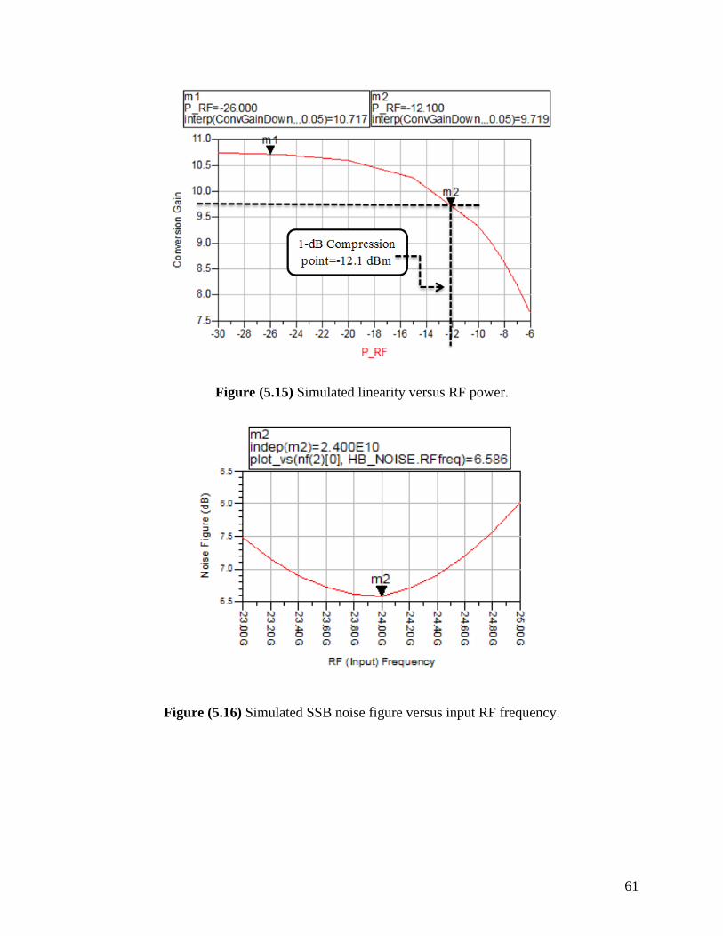
61
Figure (5.15) Simulated linearity versus RF power.
Figure (5.16) Simulated SSB noise figure versus input RF frequency.
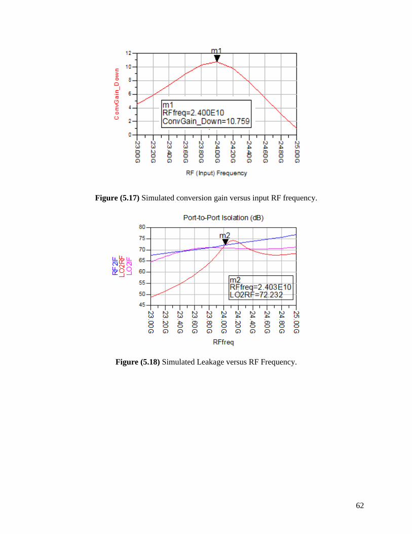
62
Figure (5.17) Simulated conversion gain versus input RF frequency.
Figure (5.18) Simulated Leakage versus RF Frequency.
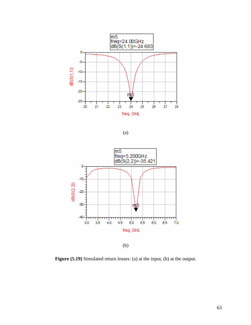
63
(a)
(b)
Figure (5.19) Simulated return losses: (a) at the input, (b) at the output.
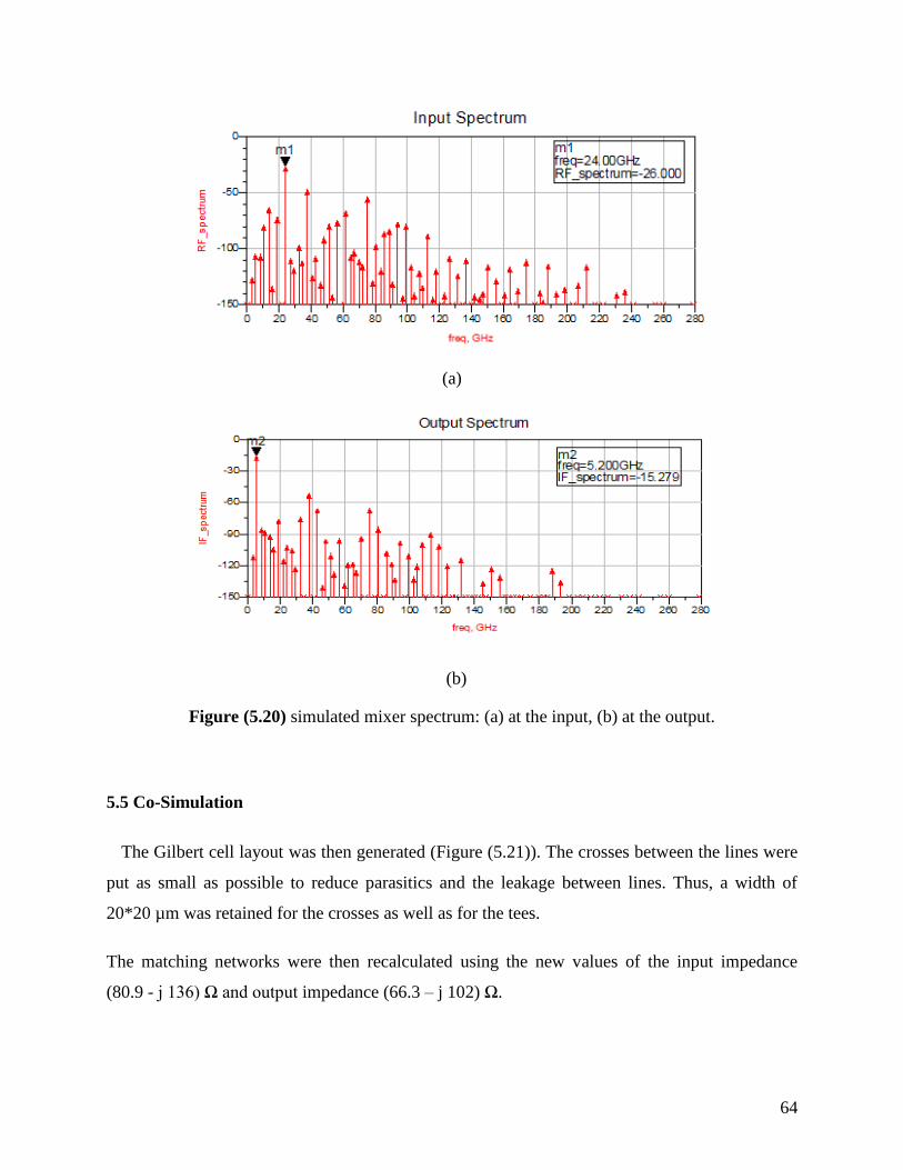
64
(a)
(b)
Figure (5.20) simulated mixer spectrum: (a) at the input, (b) at the output.
5.5 Co-Simulation
The Gilbert cell layout was then generated (Figure (5.21)). The crosses between the lines were
put as small as possible to reduce parasitics and the leakage between lines. Thus, a width of
20*20 µm was retained for the crosses as well as for the tees.
The matching networks were then recalculated using the new values of the input impedance
(80.9 - j 136) Ω and output impedance (66.3 – j 102) Ω.

65
Then, the LO power was swept to get its optimal value. Figures (5.22) and (5.23) shows the
simulated noise figure and conversion gain over the LO power, respectively. From these figures,
we can see that a LO power of -2 dBm allows getting a single sideband noise figure of around 7
dB (i.e., a double sideband noise figure of around 4 dB) and a conversion gain of 8.8 dB thus,
largely agreeing with the link budget values. We therefore, fixed the LO power to -2 dBm for the
rest of the simulations.
Note that the schematic value (0 dBm) gives quite close values as well. Figure (5.24) shows a
simulated conversion gain of 8.7 dB and a 1 dB compression point of -13.5 dBm, i.e., within the
link budget specifications. By sweeping the input frequency, Figure (5.25) and (5.26) show a
respective minimum SSB noise figure of 7 dB and gain of 8.8 dB at the center frequency.
The simulated isolation between the three ports reported good values (Figure (5.27). The
simulated input /output power spectrum shown in Figures (5.28), respectively, are also within the
desired specifications. Similar conclusions can be made for the simulated input/output return loss
shown in Figure (5.29), respectively.
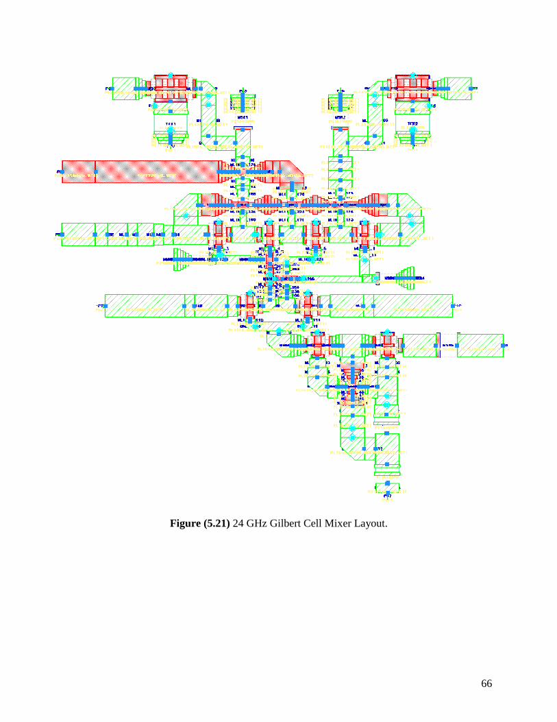
66
Figure (5.21) 24 GHz Gilbert Cell Mixer Layout.

67
Figure (5.22) Simulated noise figure versus LO Power.
Figure (5.23) Simulated gain versus LO power.

68
Figure (5.24) Simulated 1-dB Compression Point Versus RF Input power.
Figure (5.25) Simulated noise figure versus input RF frequency.
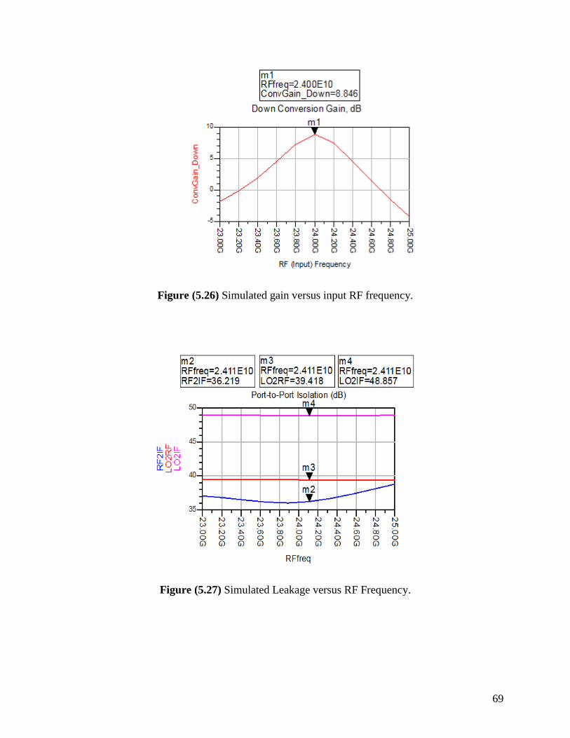
69
Figure (5.26) Simulated gain versus input RF frequency.
Figure (5.27) Simulated Leakage versus RF Frequency.

70
(a)
(b)
Figure (5.28) simulated mixer spectrum: (a) at the input, (b) at the output.
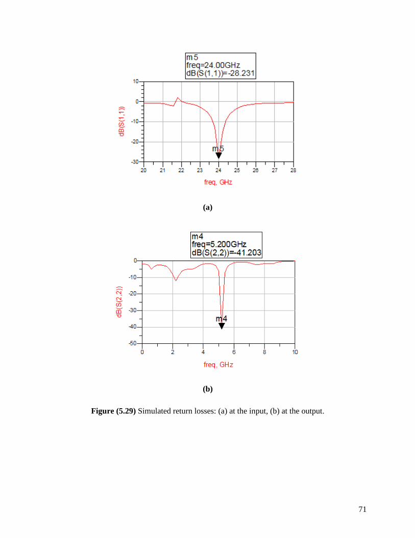
71
(a)
(b)
Figure (5.29) Simulated return losses: (a) at the input, (b) at the output.

72
5.6 Discussion
After presenting the schematic and the layout results separately, this section combines these
two results, highlighting the good agreement between them.
In fact, Figure (5.30), displaying the noise figure curves over the LO power, enhances that
despite the fact that the LO power is different, the minimum noise figure difference between the
schematic (with LO power set to 0 dB) and the layout (with LO power set to -2dB) is moderate.
Same for the conversion gain as shown in Figure (5.31).
By sweeping the RF frequency as well as the RF power, similar acceptable differences can be
found between the two designs (Figures (5.32) - (5.33) and (5.34), respectively).
Figure (5.30) noise figure curves for both schematic and layout over LO power.
6.5
6.6
6.7
6.8
6.9
7
7.1
7.2
7.3
-6 -4 -2 0 2 4
No
ise
Fiq
ure
,dB
LO Power,dBm
Schematic Layout

73
Figure (5.31) Conversion gain curves for both schematic and layout over LO power.
Figure (5.32) Noise figure curves for both schematic and layout over RF frequency.
5
6
7
8
9
10
11
-8 -6 -4 -2 0 2 4 6 8
Co
nv
ersi
on
Ga
in,d
B
LO Power,dBm
Schematic Layout
6.00
6.50
7.00
7.50
8.00
8.50
9.00
9.50
10.00
10.50
11.00
23 23.25 23.5 23.75 24 24.25 24.5 24.75 25
No
ise
Fiq
ure
,(d
B)
RF Frequency (GHz)
Schematic Layout
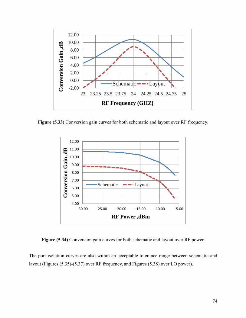
74
Figure (5.33) Conversion gain curves for both schematic and layout over RF frequency.
Figure (5.34) Conversion gain curves for both schematic and layout over RF power.
The port isolation curves are also within an acceptable tolerance range between schematic and
layout (Figures (5.35)-(5.37) over RF frequency, and Figures (5.38) over LO power).
-2.00
0.00
2.00
4.00
6.00
8.00
10.00
12.00
23 23.25 23.5 23.75 24 24.25 24.5 24.75 25
Co
nv
ersi
on
Ga
in ,d
B
RF Frequency (GHZ)
Schematic Layout
4.00
5.00
6.00
7.00
8.00
9.00
10.00
11.00
12.00
-30.00 -25.00 -20.00 -15.00 -10.00 -5.00
Co
nv
ersi
on
Gain
,d
B
RF Power ,dBm
Schematic Layout
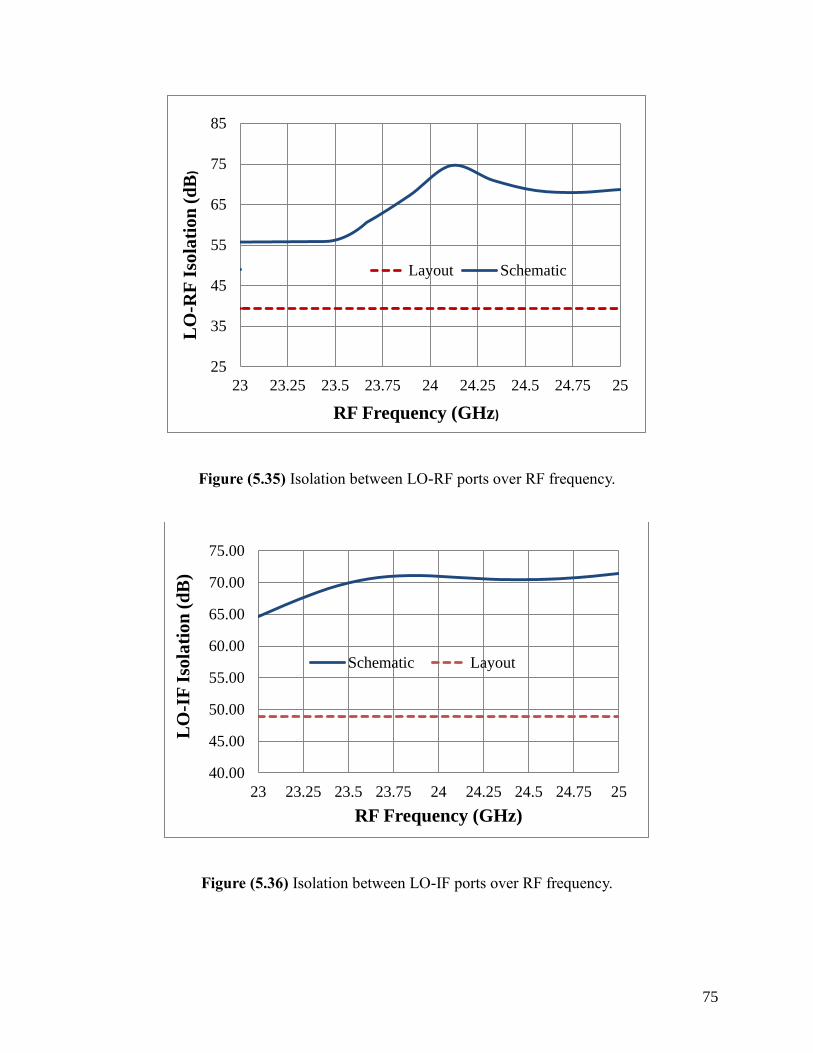
75
Figure (5.35) Isolation between LO-RF ports over RF frequency.
Figure (5.36) Isolation between LO-IF ports over RF frequency.
25
35
45
55
65
75
85
23 23.25 23.5 23.75 24 24.25 24.5 24.75 25
LO
-RF
Iso
lati
on
(d
B)
RF Frequency (GHz)
Layout Schematic
40.00
45.00
50.00
55.00
60.00
65.00
70.00
75.00
23 23.25 23.5 23.75 24 24.25 24.5 24.75 25
LO
-IF
Iso
lati
on
(d
B)
RF Frequency (GHz)
Schematic Layout
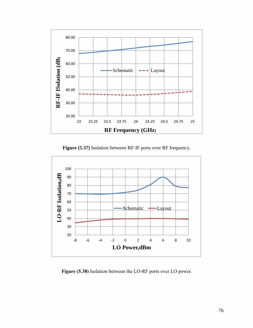
76
Figure (5.37) Isolation between RF-IF ports over RF frequency.
Figure (5.38) Isolation between the LO-RF ports over LO power.
20.00
30.00
40.00
50.00
60.00
70.00
80.00
23 23.25 23.5 23.75 24 24.25 24.5 24.75 25
RF
-IF
IS
ola
tio
n (
dB
)
RF Frequency (GHz)
Schematic Layout
20
30
40
50
60
70
80
90
100
-8 -6 -4 -2 0 2 4 6 8 10
LO
-RF
Iso
lati
on
,dB
LO Power,dBm
Schematic Layout
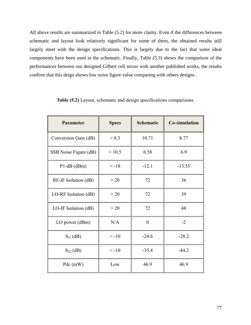
77
All above results are summarized in Table (5.2) for more clarity. Even if the differences between
schematic and layout look relatively significant for some of them, the obtained results still
largely meet with the design specifications. This is largely due to the fact that some ideal
components have been used in the schematic. Finally, Table (5.3) shows the comparison of the
performances between our designed Gilbert cell mixer with another published works, the results
confirm that this deign shows low noise figure value comparing with others designs .
Table (5.2) Layout, schematic and design specifications comparisons.
Parameter Specs Schematic Co-simulation
Conversion Gain (dB) > 8.3 10.71 8.77
SSB Noise Figure (dB) < 10.5 6.58 6.9
P1-dB (dBm) > -18 -12.1 -13.55
RF-IF Isolation (dB) > 20 72 36
LO-RF Isolation (dB) > 20 72 39
LO-IF Isolation (dB) > 20 72 48
LO power (dBm) N/A 0 -2
S11 (dB) < -10 -24.6 -28.2
S22 (dB) < -10 -35.4 -44.2
Pdc (mW) Low 46.9 46.9
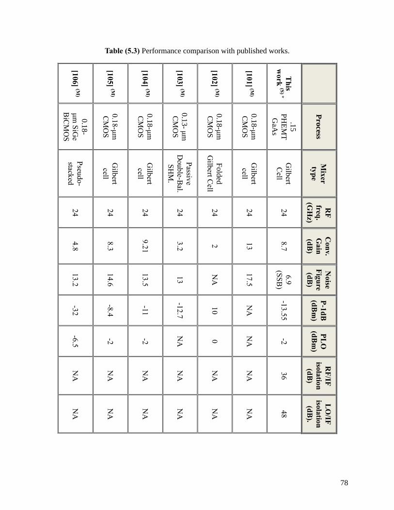
78
Table (5.3) Performance comparison with published works.
[106] (M
)
[105] (M
)
[104] (M
)
[103] (M
)
[102] (M
)
[101] (M
)
Th
is
work
(S) *
0.1
8-
μm
SiG
e
BiC
MO
S
0.1
8-μ
m
CM
OS
0.1
8-μ
m
CM
OS
0.1
3- μ
m
CM
OS
0.1
8-μ
m
CM
OS
0.1
8-μ
m
CM
OS
.15
PH
EM
T
GaA
s
Pro
cess
Pseu
do
-
stacked
Gilb
ert
cell
Gilb
ert
cell
Passiv
e
Double-B
al.
SH
M.
Fold
ed
Gilb
ert Cell
Gilb
ert
cell
Gilb
ert
Cell
Mix
er
typ
e
24
24
24
24
24
24
24
RF
freq.
(GH
z)
4.8
8.3
9.2
1
3.2
2
13
8.7
Con
v.
Gain
(dB
)
13.2
14.6
13.5
13
NA
17.5
6.9
(SS
B)
Noise
Fig
ure
(dB
)
-32
-8.4
-11
-12.7
10
NA
-13.5
5
P-1
dB
(dB
m)
-6.5
-2
-2
NA
0
NA
-2
PL
O
(dB
m)
NA
NA
NA
NA
NA
NA
36
RF
/IF
isola
tion
(dB
)
NA
NA
NA
NA
NA
NA
48
LO
/IF
isola
tion
(dB
).
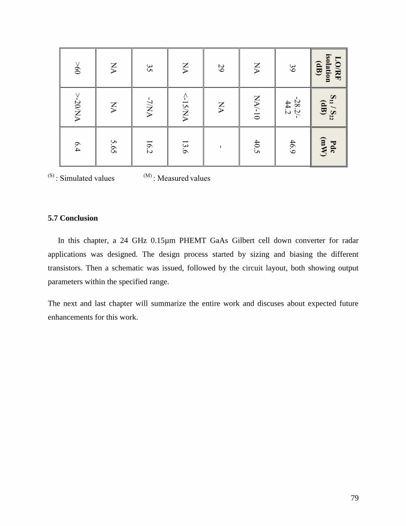
79
>60
NA
35
NA
29
NA
39
LO
/RF
isola
tion
(dB
)
>-2
0/N
A
NA
-7/N
A
<-1
5/N
A
NA
NA
/-10
-28.2
/-
44.2
S11 / S
22
(dB
)
6.4
5.6
5
16.2
13.6
-
40.5
46.9
Pd
c
(mW
)
(S) : Simulated values
(M) : Measured
values
5.7 Conclusion
In this chapter, a 24 GHz 0.15µm PHEMT GaAs Gilbert cell down converter for radar
applications was designed. The design process started by sizing and biasing the different
transistors. Then a schematic was issued, followed by the circuit layout, both showing output
parameters within the specified range.
The next and last chapter will summarize the entire work and discuses about expected future
enhancements for this work.
80
Chapter 6
Conclusions and Future Works
6.1 Conclusions
In this thesis, a 24 GHz mixer for Intelligent Transportation System (ITS) radar receiver was
designed. ITS have attracted a lot of attention because of their importance in increasing safety
and reducing road accidents.
The super-heterodyne receiver type with two mixers has been adopted. The first mixer, the
purpose of the present work, converts the 24 GHz to 5.2 GHz because of its compatible with
WLAN applications that cover emergency or police services, two of the front-line services
involved in road accidents.
The retained mixer configuration is the Gilbert cell type because, along with high gain, high
linearity, and high port isolation, it can exhibit high sensitivity, a key point in ITS receivers.
Indeed, with a conversion gain of 8.7 dB, a (SSB) noise figure of 6.9 dB, a linearity of -13.5
dBm as well as an isolation better than 30 dB, this 0.15µm pHEMT GaAs mixer largely meets
the required specifications obtained through a complete receiver link budget.
Three microstrip couplers were also designed to transform the single input/output signals to
differential signals.
6.2 Future works
In this thesis, the first mixer of a modified 24 GHz radar receiver has been designed, largely
meeting the required specification values obtained from the link budget.
However some improvements and future works can be done for this mixer and/or for the whole
the radar receiver for better performance. Some of these recommendations are as follows:
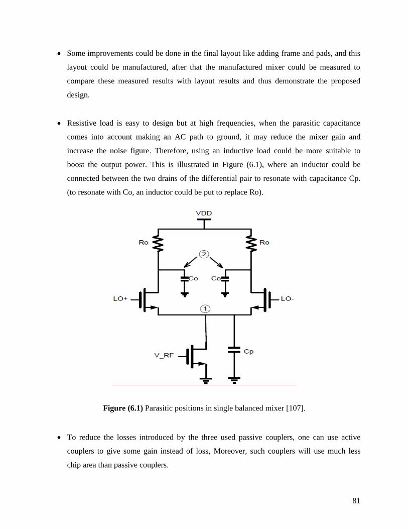
81
Some improvements could be done in the final layout like adding frame and pads, and this
layout could be manufactured, after that the manufactured mixer could be measured to
compare these measured results with layout results and thus demonstrate the proposed
design.
Resistive load is easy to design but at high frequencies, when the parasitic capacitance
comes into account making an AC path to ground, it may reduce the mixer gain and
increase the noise figure. Therefore, using an inductive load could be more suitable to
boost the output power. This is illustrated in Figure (6.1), where an inductor could be
connected between the two drains of the differential pair to resonate with capacitance Cp.
(to resonate with Co, an inductor could be put to replace Ro).
Figure (6.1) Parasitic positions in single balanced mixer [107].
To reduce the losses introduced by the three used passive couplers, one can use active
couplers to give some gain instead of loss, Moreover, such couplers will use much less
chip area than passive couplers.

82
The GaAs pHEMT has low noise performance, but at the same time consumes higher
power than CMOS technology. Therefore, some techniques like current reuse could be
used to reduce the power consumption.
The bandwidth for this mixer is narrow and it is fine for this application. However, to
expand the bandwidth for large bandwidth applications, the matching networks and
couplers could be redesigned for this purpose; another reported way to expand the
bandwidth is to put an inductor between the transconductance and the switching stage
[108].
This design could be expanded to include the whole radar receiver parts like the amplifiers,
the second mixer, the filters, etc., based on the values obtained from the receiver link
budget.

83
References
[1] World Health Organization, Official WHO health days, Last access, June 25, 2014.
http://www.who.int/mediacentre/events/official_days/en/ .
[2] L. Han, “Integrated comunication and radar scheme for future intelligent transportation
systems,” Ph.D. Thesis, École Polytechnique de Montréal, Canada, 2011.
[3] “Intelligent Transportation Systems (ITS) Strategic Plan” ITS Task Group, Alberta
Infrastructure, Last access, June 25, 2014.
http://www.transportation.alberta.ca/Content/docType52/Production/StratPlan.pdf.
[4] J. Wahle, “Information in intelligent transportation systems,” Ph.D. Thesis, Vom
Fachbereich Physik – Technologie der Universitat, 2002.
[5] L. Wang, “Millimeter-wave integrated circuits in SiGe:C technology,” Ph.D. Thesis,
Brandenburg Technical University Cottbus, 2008.
[6] K. Trichias, “Modeling and evaluation of LTE in intelligent transportation systems,”
M.Sc. Thesis, University of Twente and TNO, 2011.
[7] I. Vadim, Microwave Circuits for 24 GHz Automotive Radar in Silicon-Based
Technologies, Springer, 2010.
[8] P. Heide, M. Vossiek, M. Nalezinski, L. Oreans, R. Schubert, and M. Kunert, “24 GHz
short-range microwave sensors for industrial and vehicular Applications,” Short-Range
Radar Workshop, Il-Menau, Germany, 1999.
[9] S. Luo, R. Hung, S. Weng, Y. Ye, C. Chuang, C. Lin, and H. Chang, "24-GHz MMIC
development using 0.15-µm GaAs PHEMT process for automotive radar applications,"
Asia-Pacific Microwave Conf., pp. 1-4, 2008.
[10] V. Cojocaru, H. Kurata, D. Humphrey, B. Clarke, T. Yokoyama, V. Napijalo, T. Young,
and T. Adachi, "A 24GHz low-cost, long-range, narrow-band, monopulse radar front end
system for automotive ACC applications," Int. IEEE/MTT Microwave Symp., pp. 1327-
1330, 2007.
84
[11] L. Varshney, “Radar system components and system design,” Technical Report,
Syracuse Research Corp., Last access, June 25, 2014.
http://www.ifp.illinois.edu/~varshney/cornell/publications/radar%20system%20compone
nts%20and%20system%20design.pdf.
[12] Radar Range equation, Last access, June 26, 2014,
http://www.ece.uah.edu/courses/material/EE6192011/RadarRangeEquation%282%29201
1.pdf.
[13] Math Works, Radar Equation, Last access, June, 2014.
http://www.mathworks.com/help/phased/ug/radar-equation.html.
[14] Y. Chan and V. Koo, “An introduction to synthetic Aperture Radar (SAR)”, Progress In
Electromagnetic research B, Vol. 2, pp. 27-60, 2008.
[15] D. Ma, “RF receiver systems and circuits,” 1371 Term Paper, Last access, June 25, 2014
http://qtwork.tudelft.nl/~schouten/linkload/rfreceivers1.pdf.
[16] P. Yue, “Receiver architecture slides-source”, Last access, June 25, 2014
http://course.ee.ust.hk/elec528/Notes/Lec4-1-basic-Rx-arch.pdf.
[17] M.T. Safdar, “Super-regenerative receiver for short-range HF band applications,” M.Sc.
Thesis, Halmstad University, 2008.
[18] A. Behzad, Wireless LAN Radios: System Definition to Transistor Design, Wiley-IEEE
Press, 2007.
[19] X. Wang, “Linear zero-IF direct conversion receiver,” M.Sc. Thesis, Universität
Duisburg-Essen, 2006.
[20] C. Hsieh, “Wide frequency range superhetrodyne receiver design and simulation,” M.Sc.
Thesis, Concordia University, 2011.
[21] A. Niknejad, “Receiver architectures,” Course Notes, Advanced Communication
Integrated Circuits, University of California, Last access, 26 June 2014
http://rfic.eecs.berkeley.edu/~niknejad/ee242/pdf/eecs242_lect3_rxarch.pdf.

85
[22] “Attenuators Design Tutorial; RF, RFIC and Microwave theory and design,” Last access,
June 25, 2014.
http://www.odyseus.nildram.co.uk/RFMicrowave_Circuits_Files/Attenuator.pdf.
[23] http://www.ntia.doc.gov/files/ntia/publications/compendium/2900.00-
3100.00_01MAR14.pdf, Last access, June 16, 2014.
[24] F. Gong, “Front end circuit module designs for a digitally controlled channelized
SDR receiver architecture,” Ph.D. Thesis, Ohio State University, 2011.
[25] S. Buttrich, “Radio link calculation,” Last access, June 25, 2014
http://wire.less.dk/wiki/images/0/0b/Wireless_link_budget_slides_edit_nepal.pdf
[26] L. Mengxiong, "5 GHz optical front end in 0.35 um CMOS." Ph.D. Thesis, University of
Nottingham, 2007.
[27] A. Sadiq and E. Arabi. "Behavioural modeling of RF front end devices in Simulink."
M.Sc. Thesis, Chalmers University of Technology, 2008.
[28] Y. Lam,” 1.2V CMOS down conversion mixer and VCO design for RF front-end
transceiver applications”, M.Sc. Thesis, McMaster University, 2003.
[29] I. Rosu, “Understanding noise figure”, last access May, 10, 2014.
http://www.qsl.net/va3iul/Noise/Understanding%20Noise%20Figure.pdf.
[30] X. Guan, “Microwave integrated phased array receivers in silicon,” Ph.D. Thesis,
Caltech, 2005.
[31] M. Soer. “Analysis and comparison of switch-based frequency converters,” M.Sc. Thesis,
University of Twente, Netherlands, 2007.
[32] “RF Microelectronic, LNA, Mixer and oscillator,” last access, May 10, 2014
http://www.slideserve.com/cicero/rf-microelectronic
[33] S. Long, “Mixer Lectures ECE145B/ECE218B,” last access May 10, 2014.
http://www.ece.ucsb.edu/Faculty/rodwell/Classes/ece218b/notes/Mixer1.pdf.

86
[34] K. MacClaning, Wireless Receiver Design for Digital Communication, 2nd
Ed., SciTech
Publishing Inc., 2000.
[35] P. Lindberg, "Radio frequency integrated circuits for 24 GHz radar applications." Ph.D.
Thesis, Uppsala University, 2005.
[36] K. Miehle, "A new linearization method for cancellation of third order distortion." Ph.D.
Thesis, University of North Carolina, 2003.
[37] C. Cho, “RF Circuit Nonlinearity Characterization and Modeling for Embedded Test,"
Ph.D. Thesis, University of Florida, 2005.
[38] M. Loy, “Understanding and Enhancing Sensitivity in Receivers for Wireless
Applications”, Texas Instruments, Technical brief, last access, May, 2014.
http://www.ti.com/lit/an/swra030/swra030.pdf.
[39] J. Rogers and C. Plett, Radio Frequency Integrated Circuit Design, 2nd
Ed., Artech
House, 2010.
[40] M. Abbassi,” Characterization of a 5 GHz modular radio front end for WLAN based on
IEEE 802.11p,” M.A.Sc. Thesis, University of Gavle, 2008.
[41] X. Guan, "Microwave integrated phased array receivers in silicon," Ph.D. Thesis,
California Institute of Technology, 2006.
[42] RF Café, “Cascaded 1 dB Compression Point (P1 dB),” Last access, June 25, 2014
http://www.rfcafe.com/references/electrical/p1db.htm.
[43] A. Almohamaideed, “Down-converter Gilbert-Cell mixer for WiMax applications using
0.15μm GaAs HEMT technology,” M.A.Sc. Thesis, University of Ottawa, 2014.
[44] J. Karki, “Calculating noise figure and third-order intercept in ADCs”, Texas Instruments,
Last access, May, 2014. http://www.ti.com/lit/an/slyt090/slyt090.pdf.
[45] “More notes on intercept points,” Signal Processing Group Inc., Last access, May, 2014,
http://www.signalpro.biz/pointsf1.pdf.
[46] A. Meaamar "An ultra-wideband receiver front-end," Ph.D. Thesis, Nanyang
Technological University, 2010.

87
[47] A. Siddiqi, “Design methodology and investigation of GHz range CMOS RF mixers,”
M.Sc. Thesis, Ottawa University, 2000.
[48] N. Poobuapheun, “LNA and mixer designs for multi-band receiver front-ends,” Ph.D.
Thesis, University of California, 2009.
[49] S. Lee,” Design and analysis of ultra-wide band width impulse radio receiver”, PHD
thesis, University of Southern California, August 2002.
[50] A. Serban, “Ultra-wideband low-noise amplifier and six-port transceiver for high speed
data transmission,” Ph.D. Thesis, Norrkoping, 2010.
[51] A. Matsuzawa, “RF circuits design: Basics”, Tokyo Institute of Technology, Last access,
May 12, 2014,
http://www.ssc.pe.titech.ac.jp/materials/VLSICS03_shortcourse_matsu_homepage.pdf.
[52] J. Lerdworatawee, W. Namgoong, “Revisiting spurious-free dynamic range of
communication receivers, “IEEE Trans. Circuits Syst., vol. 53, pp. 937-943, 2006.
[53] M. Baker, “A BiCMOS RF mixer for 5-GHz receivers,” Ph.D. Thesis, Massachusetts
Institute of Technology, 2002.
[54] Application Note 103 – Dynamic Range and Noise, Last access, May 10, 2014
http://www.icrf.nl/LinkClick.aspx?fileticket=GlJu7C/cWSQ=&tabid=2943.
[55] L. Asbrink, “Blocking Dynamic Range in Receivers,” Last access, May 10, 2014.
http://www.sm5bsz.com/dynrange/qex/bdr.pdf.
[56] Notes for Blocking Dynamic Range, last access, May 12, 2014
http://www.adventure-radio.org/ars/pages/lab_text/notes_bdr.html.
[57] B.L. Fox, “Analysis and dynamic range enhancement of the analog-to digital interface in
multimode radio receivers,” Master’s Thesis, Virginia Polytechnic Institute and State
University, 1997.
[58] P. Alegre, “Analysis, design and implementation of analog/RF blocks suitable for a
multi-band analog interface for CMOS SOCs.,” Ph.D. Thesis, Universidade Federal do
Rio Grande do Sul, 2008.
88
[59] Q. Wan, C. Wang, and J. Sun, “Design of a low voltage highly linear 2.4 up-conversion
mixer in 0.18 um CMOS technology,” Wireless Personnel Communication.
[60] M.C.E. Yagoub. “Non-linear microwave circuits”, ELG6369 Course Notes, 2012.
[61] F. Giannini and G. Leuzzi. Nonlinear Microwave Circuit Design, J. Wiley & Sons, 2004.
[62] Dual-gate FET Mixer, Last access, May 10, 2014,
http://home.sandiego.edu/~ekim/otherjunk/dualfet1.pdf.
[63] J. Park, “A highly linear and low flicker-noise CMOS direct conversion receiver front-
end for multiband applications,” Ph.D. Thesis, Georgia Institute of Technology, 2007.
[64] E. Klumperink et al., “A CMOS switched transconductor mixer,” IEEE J. Solid-State
Circuits, vol. 39, pp. 1231–1240, 2004.
[65] V. Vidojkovic, J. Tang, A. Leeuwenburgh, and A. Roermund, “A low-voltage folded-
switching mixer in 0.18-μm CMOS," IEEE J. Solid-State Circuits, vol. 40, pp. 1259-
1264, 2005.
[66] L.K. Hao, H. Y. Chang, and Y. J. Chan. "High linearity and low-power RF CMOS mixers
for wireless communication." Ph.D. Thesis, National Central University, 2008.
[67] R. Hedayati, S. Haddadian, and H. Nabouvati, “A low voltage high linearity CMOS
Gilbert cell using charge injection method,” World Academy of Science, Engineering and
Technology, vol. 38, pp. 147-151, 2008.
[68] H. Kang, "Gain and noise improvement technique mixer for 2.4 & 5.2 GHx dual band
direct conversion receiver," M.Sc. Thesis, School of Engineering information and
communication University, 2007.
[69] M. Vidojkovic. "Configurable circuits and their impact on multi-standard RF front-end
architecture," Ph.D. Thesis, Technische Universiteit Eindhoven, 2011.
[70] “Up converting modulated signals to microwave with an external mixer and the R&S
SMF100A microwave signal generator,” last access, May 12, 2014.
http://cdn.rohdeschwarz.com/dl_downloads/dl_application/application_notes/1gp65/1GP
65_0E.pdf.
89
[71] T. K. Saravanan. "Analysis and design of successive approximation ADC and 3.5 GHz
RF transmitter in 90nm CMOS." M.Sc. Thesis, Georgia Institute of Technology, 2010.
[72] M.M.M. Elkholy, “CMOS receiver front-end design for WCDMA,” M.Sc. Thesis, Ain
Shams University, 2011.
[73] J. Li, “Nano-metric optimized CMOS RF receiver front-end components for UHF RFID
readers,” Ph.D. Thesis, Massey University, 2011.
[74] N. Nayak, “Active transistor mixer”, M.Sc. Thesis, California State University, 2011.
[75] V. Von, “Design of CMOS mixers and receiver integration for high precision local
positioning systems”, Ph.D. Thesis, Elektrotechnik und Informatik der Technischen
Universität, 2011.
[76] Z. Su and Z. Lin, "A 18.9dB conversion gain folded mixer for WiMAX system," IEEE
Asia Pacific Conf. Circuits and Systems, pp. 292-295, 2008.
[77] S. Long, “Presentation on RFIC MOS Gilbert cell mixer design”, Agilent EEsof EDA,
Last access, May 10, 2014, http://cp.literature.agilent.com/litweb/pdf/5989-9103EN.pdf
[78] G. Liu, “A 60 GHz, multi-Gbps down-converter IC in an 80 GHz fT SiGe technology”,
Ph.D. Thesis, Universität Ulm, 2012.
[79] Y. Sun, “Design of an Integrated 60 GHz Transceiver Front-End in SiGe:C BiCMOS
Technology,” Ph.D. Thesis, Brandenburgischen Technischen Universitat, 2009.
[80] F. Xiangning, Z. Chisheng, and Z. Lei, "A 2.4 GHz RF CMOS up-conversion mixer for
wireless sensor networks nodes," Int. Conf. Wireless Communications and Signal
Processing, pp. 1-5, 2009.
[81] A. Verma, “Design and characterization of frequency conversion circuits for wireless
applications,” Ph.D Thesis, University of Florida, 2006.
[82] A. Ruhumbika and R. Abdulla, “Analytical method for gain analysis of a double balanced
gilbert cell mixer,” Int. Conf. on Technological Advances in Electrical, Electronics and
Computer Engineering, Kuala Lumpur, Malaysia, pp. 193-198, 2014.
[83] Y. Zhang, “Study of uniplanar phase inverter ring coupler and magic-tee circuits,” Master
Thesis, Ecole Polytechnique de Montreal, 2001.
90
[84] T. Yassin, “Development and manufacturing of direct antenna integrated RF Front-End
for ice sounding radar,” M.Sc. Thesis, Technical University of Denmark, 2006.
[85] V. Issakov, A. Thiede, and V. Winkler, "An analytical insight on the frequency behaviour
of rat-race coupler," German Microwave Conf., pp. 82-85, 2008.
[86] D. Jasteh, “Isolation enhancement in a dual port antenna,” M.Sc. Thesis, University of
Birmingham, 2011.
[87] A. Kachayev, “LIGA-micromachined tight microwave couplers,” M.Sc. Thesis,
University of Saskatchewan, 2003.
[88] C.S. Sierra, "Microwave directional couplers,” M.Sc. Thesis, Universita Degli Studi di
Brescia, 2010.
[89] M.L. Edwards, Microwave and RF Circuits: Analysis, Design, Fabrication, and
Measurement, Johns Hopkins University, 2001.
[90] M. Rahman, “Miniaturized quadrature hybrid and rat race coupler utilizing coupled lines
for LTE Frequency bands,” M.Sc. Thesis, Norrkoping, 2013.
[91] C. Lin, P. Wu, H. Chang, and H. Wang, "A 9-50-GHz Gilbert-cell down-conversion
mixer in 0.13-µm CMOS technology," IEEE Microwave and Wireless Components Lett.,
vol. 16, pp. 293-295, 2006.
[92] M. Wang, “Reconfigurable CMOS mixers for radio-frequency applications,” M.A.Sc.
Thesis, Queen’s University, 2010.
[93] Z. Su and Z. Lin, "A 18.9dB conversion gain folded mixer for WiMAX system," IEEE
Asia Pacific Conf. Circuits and Systems, pp. 292-295, 2008.
[94] C. Breadendiek, N. Phole, T. Jaeschke, K. Aufinger, and A. Bilgic, “A highly-linear low
power down-conversion mixer for monostatic broad-band 80 GHz FMCW – radar
transceivers,” Progress in Electromagnetic Research Symp., 2012.
[95] V. Chandra, “A 2.5 V high linearity CMOS mixer for 1.9 GHz applications," Carnegie
Melon University, 2002.
[96] S.H. Zhou, "The design of CMOS RF mixer based on Gilbert cell," IEEE Symp.
on Electrical and Electronics Eng., pp. 392-395, 2012.

91
[97] Y.S. Youn, N. S. Kim, J.H. Chang, Y.J. Lee, and H.K. Yu, “A RF front-End CMOS
Transceiver for 2GHz Dual-Band Applications”, J. of Semiconductor Technology and
Science, Vol. 2, pp. 147-155, 2002.
[98] A. Angelov, “System level analysis of a direct-conversion WiMax receiver at 5.3 GHz
and corresponding mixer design,” Master Thesis, Technical University of Cret, 2008.
[99] A. Khy and B. Huyart, "A (35 – 45) GHz low power direct-conversion gilbert-cell mixer
in 0.13μm GaAs pHEMT technology," European Microwave Conf., pp. 1058-1061, 2010.
[100] W.N. Chen, K.H. Cheng, and T.Y. Hsueh, "A low power Gilbert mixer for 10GHz
application using TSMC 0.18μm CMOS RF technology," Int. Conf. Solid-State and
Integrated Circuit Technology, pp. 1559-1561, 2006.
[101] X. Guan and A. Hajimiri, “A 24 GHz CMOS front-end,” IEEE Eur. Solid-State Circuits
Conf., pp. 155–158, 2002.
[102] M. Hossain, M. Frank, and M. Antar, "Performance of a low voltage highly linear 24
GHz down conversion mixer in 0.18μm CMOS," Topical Meeting on Silicon Monolithic
Integrated Circuits in RF Systems, pp. 18-20, 2006.
[103] R.M. Kodkani, L. Larson, “A 24 GHz CMOS direct-conversion sub-harmonic down
converster,” RFIC Symp., pp. 485-488, 2007.
[104] D. Ahn, D.-W. Kim, and S. Hong, “A K-band high-gain down-conversion mixer in
0.18μm CMOS technology,” IEEE Microwave Wireless Compon. Lett., vol. 19, pp. 227-
229, 2009.
[105] Y.H. Chang, C.Y. Huang, and Y.C. Chiang, "A 24GHz down-conversion mixer with low
noise and high gain," European Microwave Integrated Circuits Conf., pp. 285-288, 2012.
[106] N. Shiramizu, T. Masuda, T. Nakamura, and K. Washio, “24-GHz 1-V pseudo- stacked
mixer with gain-boosting technique,” IEEE Eur. Solid-State Circuits Conf., pp. 102–105,
2008.
[107] M. Beigizadeh and A. Nabavi "A K-band common-source Gilbert-cell mixer with high
gain and high linearity for UWB applications," Iranian Conf. on Electrical Engineering
pp. 1-5, 2013.

92
[108] H. Naderian, A. Hakimi, and M. Movahhedi, "A wideband low-noise downconversion
mixer with positive-negative feedbacks," Iranian Conf. on Electrical Engineering, pp.
206-210, 2012.
[109] EE 3.02/A04 Instrumentation, “Noise”, Last access, June 25, 2014
http://cas.ee.ic.ac.uk/people/dario/files/E302/2-noise.pdf.
[110] Hittite Microwave Corp., Last access, June 25, 2014
http://www.hittite.com/content/documents/data_sheet/hmc751lc4.pdf.
[111] Date Sheet, ATN 3590 Series: Fixed Attenuators, Sky Works, Last access, June 25, 2014,
http://www.skyworksinc.com/uploads/documents/ATN3590_Series_200842D.pdf.
[112] Analog Devices, “50 MHz to 6 GHz RF/IF gain blocks, preliminary technical data,” ADL
5541/ADL 5542, Last access June 2014.
http://www.analog.com/static/imported-files/data_sheets/ADL5542.pdf.
[113] Band Pass Filter, BFCN-2900+, 2700-3100 MHz, Last access, June 25, 2014
http://www.minicircuits.com/pdfs/BFCN-2900+.pdf.
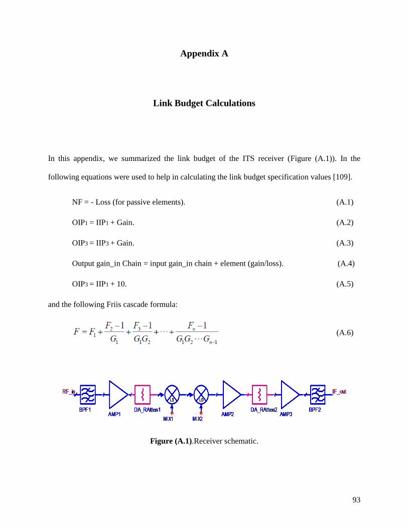
93
Appendix A
Link Budget Calculations
In this appendix, we summarized the link budget of the ITS receiver (Figure (A.1)). In the
following equations were used to help in calculating the link budget specification values [109].
NF = - Loss (for passive elements). (A.1)
OIP1 = IIP1 + Gain. (A.2)
OIP3 = IIP3 + Gain. (A.3)
Output gain_in Chain = input gain_in chain + element (gain/loss). (A.4)
OIP3 = IIP1 + 10. (A.5)
and the following Friis cascade formula:
(A.6)
Figure (A.1).Receiver schematic.
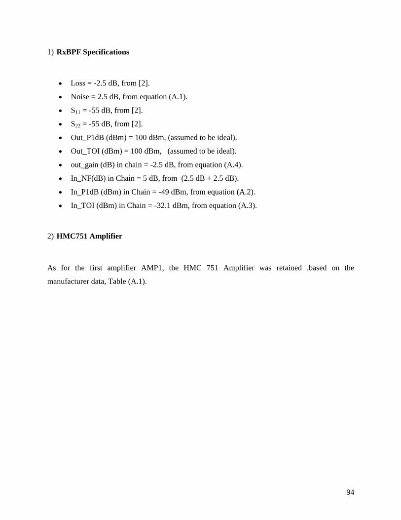
94
1) RxBPF Specifications
Loss = -2.5 dB, from [2].
Noise = 2.5 dB, from equation (A.1).
S11 = -55 dB, from [2].
S22 = -55 dB, from [2].
Out_P1dB (dBm) = 100 dBm, (assumed to be ideal).
Out_TOI (dBm) = 100 dBm, (assumed to be ideal).
out_gain (dB) in chain = -2.5 dB, from equation (A.4).
In_NF(dB) in Chain = 5 dB, from (2.5 dB + 2.5 dB).
In_P1dB (dBm) in Chain = -49 dBm, from equation (A.2).
In_TOI (dBm) in Chain = -32.1 dBm, from equation (A.3).
2) HMC751 Amplifier
As for the first amplifier AMP1, the HMC 751 Amplifier was retained .based on the
manufacturer data, Table (A.1).

95
(Table A.1) HMC 751 parameters [110].
Parameter Min. Typ. Max. Min. Typ. Max. Units
Frequency Range 17-20 20-27 GHz
Gain 22 24 23 25 dB
Gain variation over Temperature 0.025 0.028 dB/C
Noise Figure 2.2 2.8 2 2.6 dB
Input Return Loss 17 15 dB
Output return Loss 16 15 dB
Output Power for 1dB Compression (P1dB) 13 13 dBm
Saturated output Power (Psat) 15 15 dBm
Output Third Order Intercept (IP3) 25 25 dBm
Supply Current (Idd)(Vdd=+4) 50 73 90 50 73 90 mA
We have then:
Gain = 25 dB, from Table (A.1).
Noise Figure = 2.1 dB, from Table (A.1).
S11 = -15 dB, from Table (A.1).
S22 = -15 dB, from Table (A.1).
Out_P1dB (dBm) in Chain=13 dBm, from Table (A.1).
Out_TOI (dBm) in Chain = 25 dBm, from the Table (A.1).
Out_gain in chain = 22.3 dB, from equation (A.4).

96
Out_P1dB (dBm) in Chain =12.8 dBm, from [2].
Out_TOI (dBm) in Chain=25 dBm, from [2].
IN_NF (dB) in Chain = 6.3 dB, from equation (A.6).
In_P1dB (dBm) in Chain = -24 dBm, from equation (A.2).
In_TOI (dBm) in Chain = -7.1 dBm, from equation (A.3).
3) ATN3590
From data sheets for this attenuator, [111] (Figure (A.2)).
Gain =-3 dB, from Figure (A.2).
S11 = -100 dB, (assumed to be ideal).
S22 = -100 dB, (assumed to be ideal).
Out_P1dB (dBm) of Comp. = 100 dBm (assumed to be ideal).
Out_TOI (dBm) of Comp. = 100 dBm (assumed to be ideal).
NF (dB) of Comp. = 3 dB, from equation (A.1).
Out_Gain (dB) in Chain = 19.5 dB, from equation (A.4).
Out_P1dB (dBm) in Chain = 9.7 dBm,from ref (2).
Out_TOI (dBm) in Chain = 21.6 dBm, from ref (2).
In_NF(dB) in Chain = 6.31 dB ,from equation (A.6).
In_P1dB (dBm) in Chain = -27 dBm, from equation (A.2).
In_TOI (dBm) in Chain = -10.1 dBm, from equation (A.3).
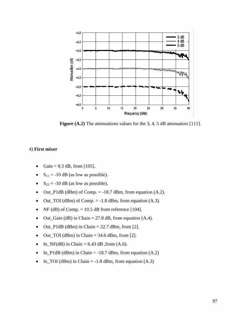
97
Figure (A.2) The attenuations values for the 3, 4, 5 dB attenuators [111].
4) First mixer
Gain = 8.3 dB, from [105].
S11 = -10 dB (as low as possible).
S22 = -10 dB (as low as possible).
Out_P1dB (dBm) of Comp. = -18.7 dBm, from equation (A.2).
Out_TOI (dBm) of Comp. = -1.8 dBm, from equation (A.3).
NF (dB) of Comp. = 10.5 dB from reference [104].
Out_Gain (dB) in Chain = 27.8 dB, from equation (A.4).
Out_P1dB (dBm) in Chain = 22.7 dBm, from [2].
Out_TOI (dBm) in Chain = 34.6 dBm, from [2].
In_NF(dB) in Chain = 6.43 dB ,from (A.6).
In_P1dB (dBm) in Chain = -18.7 dBm, from equation (A.2)
In_TOI (dBm) in Chain = -1.8 dBm, from equation (A.3)
98
5) Second mixer
Gain = -.4 dB, to keep the output gain for whole the receiver constant.
S11 = -10 dB (as low as possible).
S22 = -10 dB (as low as possible).
Out_P1dB (dBm) of Comp. = -19.1 dBm, from equation (A.2).
Out_TOI (dBm) of Comp. = -2.2 dBm, from equation (A.3).
NF (dB) of Comp. = .4 dB, from equation (A.1).
Out_Gain (dB) in Chain = 27.4 dB, from equation (A.4).
Out_P1dB (dBm) in Chain = 17.7 dBm, from [2].
Out_TOI (dBm) in Chain = 29.6 dBm, from [2].
In_NF(dB) in Chain =6.43 dB, from equation (A.6).
In_P1dB (dBm) in Chain = -19.1 dBm, from equation (A.2).
In_TOI (dBm) in Chain = -2.2 dBm ,from equation (A.3).
6) Second amplifier (ADL 5542)
From the data sheet for this Amplifier [112] (Figure (A.3)).
Figure (A.3) N.F, gain, P1dB, and OIP3 specifications for ADL 5542 [112].

99
Gain = 19 dB, from Figure (A.3).
S11 = -9 dB, from [2].
S22 = -9 dB, from [2].
Out_P1dB (dBm) of Comp. =14.7 dBm from Figure (A.3).
Out_TOI (dBm) of Comp. =36 dBm from Figure (A.3).
NF (dB) of Comp. = 3.9 dB from Figure (A.3).
Out_Gain (dB) in Chain = 46.4 dB, from equation (A.2).
Out_P1dB (dBm) in Chain = 11.5 dBm, from [2].
Out_TOI (dBm) in Chain = 22 dBm, from [2].
In_NF(dB) in Chain = 6.44 dB ,from equation (A.6).
In_P1dB (dBm) in Chain = -.1 dBm, from equation (A.2).
In_TOI (dBm) in Chain = 16.8 dBm, from equation (A.3).
7) Second attenuator
From the same data sheet reference [111]
Gain = -3 dB, from Figure (A.2).
S11 = -100 dB (assumed to be ideal).
S22 = -100 dB (assumed to be ideal).
Out_P1dB (dBm) of Comp. = 100 dB (assumed to be ideal).
Out_TOI (dBm) of Comp. = 100 dB (assumed to be ideal).
NF (dB) of Comp. = 3 dB, from equation (A.1).
Out_Gain (dB) in Chain = 43.4 dB, from equation (A.4).
Out_P1dB (dBm) in Chain = 8 dBm, from [2].
Out_TOI (dBm) in Chain = 18.4 dBm, from [2].
In_NF(dB) in Chain =6.58 dB, from equation (A.6).
In_P1dB (dBm) in Chain = -3.1 dBm, from equation (A.2).
In_TOI (dBm) in Chain = 13.8 dBm, from equation (A.3).
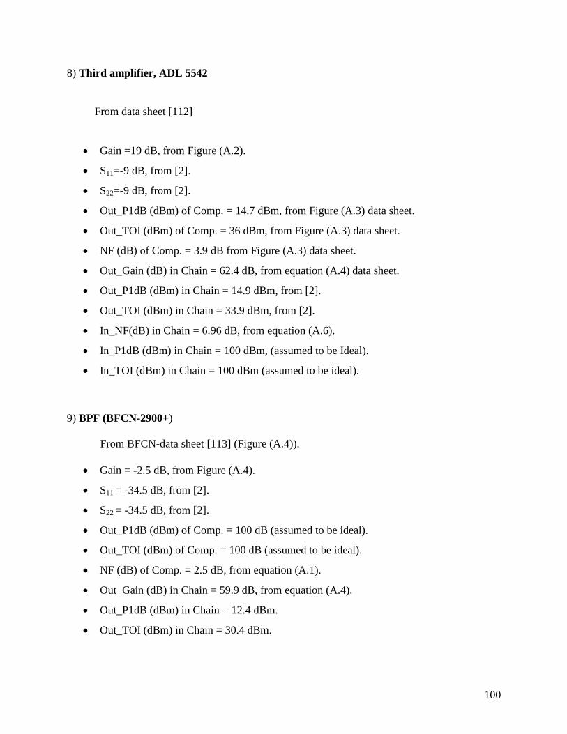
100
8) Third amplifier, ADL 5542
From data sheet [112]
Gain =19 dB, from Figure (A.2).
S11=-9 dB, from [2].
S22=-9 dB, from [2].
Out_P1dB (dBm) of Comp. = 14.7 dBm, from Figure (A.3) data sheet.
Out_TOI (dBm) of Comp. = 36 dBm, from Figure (A.3) data sheet.
NF (dB) of Comp. = 3.9 dB from Figure (A.3) data sheet.
Out_Gain (dB) in Chain = 62.4 dB, from equation (A.4) data sheet.
Out_P1dB (dBm) in Chain = 14.9 dBm, from [2].
Out_TOI (dBm) in Chain = 33.9 dBm, from [2].
In_NF(dB) in Chain = 6.96 dB, from equation (A.6).
In_P1dB (dBm) in Chain = 100 dBm, (assumed to be Ideal).
In_TOI (dBm) in Chain = 100 dBm (assumed to be ideal).
9) BPF (BFCN-2900+)
From BFCN-data sheet [113] (Figure (A.4)).
Gain = -2.5 dB, from Figure (A.4).
S11 = -34.5 dB, from [2].
S22 = -34.5 dB, from [2].
Out_P1dB (dBm) of Comp. = 100 dB (assumed to be ideal).
Out_TOI (dBm) of Comp. = 100 dB (assumed to be ideal).
NF (dB) of Comp. = 2.5 dB, from equation (A.1).
Out_Gain (dB) in Chain = 59.9 dB, from equation (A.4).
Out_P1dB (dBm) in Chain = 12.4 dBm.
Out_TOI (dBm) in Chain = 30.4 dBm.
101
Figure (A.4) BFCN-2900+: Electrical specifications [113].

102
Appendix B
Substrate Parameters
Figure (B.1): GaAs substrate layers.
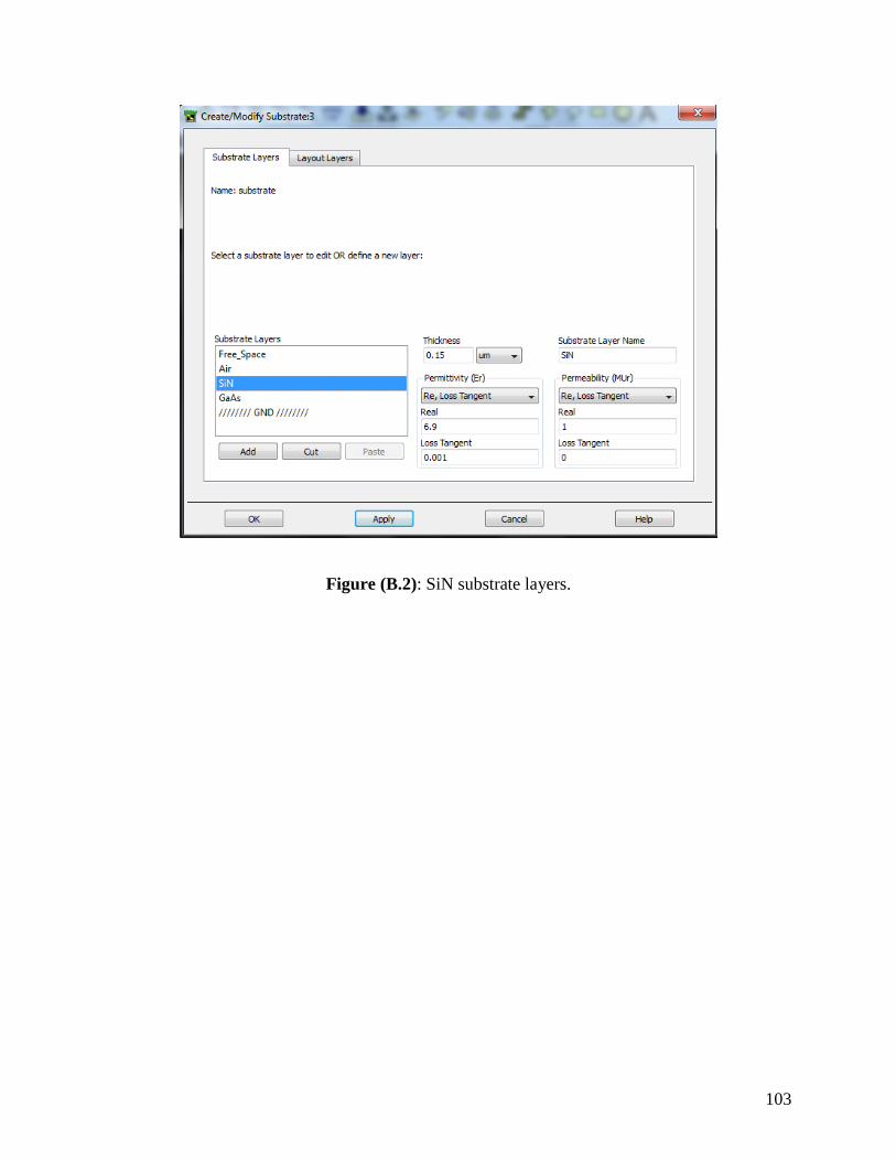
103
Figure (B.2): SiN substrate layers.

104
Figure (B.3): Air substrate layers.
![RECENT PROGRESS IN 3D/MULTILAYER MMIC ... · Web viewLow loss [10] TI / Triquint Polyimide 25 m 1 Au GaAs PHEMT Low cost, PA, LNA [11] Toshiba BCB 10 m 1 Au GaAs PHEMT MM-wave MMIC](https://img.pdfslide.us/doc/110x75/6128664f46793703e6310aec/recent-progress-in-3dmultilayer-mmic-web-view-low-loss-10-ti-triquint-polyimide.jpg)

![Инструкция Eleyus Modul 1200-70 LED SMD IS, Eleyus Modul ... file>hm\Z]bihdmip \ >eyi ^l\_j^`_ggyijZ\ZgZ]ZjZgl cg_h[kem]h\m\Zggyijhkbfh](https://img.pdfslide.us/doc/110x75/5e0b56a2ad4725484512c29c/f-eleyus-modul-1200-70-led-smd-is-eleyus-modul-gthmzbihdmip.jpg)