Embed Size (px)
Citation preview
0250M–PLD–7/10
High-performanceElectricallyErasableProgrammableLogic Device
Atmel ATF22V10B
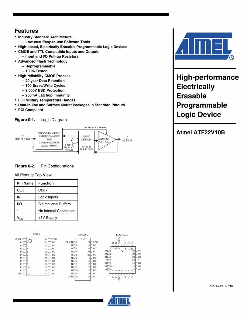
Features• Industry Standard Architecture
– Low-cost Easy-to-use Software Tools• High-speed, Electrically Erasable Programmable Logic Devices• CMOS and TTL Compatible Inputs and Outputs
– Input and I/O Pull-up Resistors• Advanced Flash Technology
– Reprogrammable– 100% Tested
• High-reliability CMOS Process– 20 year Data Retention– 100 Erase/Write Cycles– 2,000V ESD Protection– 200mA Latchup Immunity
• Full Military Temperature Ranges• Dual-in-line and Surface Mount Packages in Standard Pinouts• PCI Compliant
Figure 0-1. Logic Diagram
Figure 0-2. Pin Configurations
All Pinouts Top View
Pin Name Function
CLK Clock
IN Logic Inputs
I/O Bidirectional Buffers
* No Internal Connection
VCC +5V Supply
123456789101112
242322212019181716151413
CLK/INININININININININININ
GND
VCCI/OI/OI/OI/OI/OI/OI/OI/OI/OI/OIN
DIP/SOIC
567891011
25242322212019
INININ
*INININ
I/OI/OI/O*I/OI/OI/O
4 3 2 1 28 27 26
12 13 14 15 16 17 18
IN ING
ND *
IN I/O I/O
IN IN CLK
/IN* V
CC
I/O I/O
LCC/PLCC
123456789101112
242322212019181716151413
CLK/INININININININININININ
GND
VCCI/OI/OI/OI/OI/OI/OI/OI/OI/OI/OIN
TSSOP
1. DescriptionThe Atmel® ATF22V10B is a high-performance CMOS (electrically erasable) programmable logic device (PLD)which utilizes the Atmel proven electrically erasable Flash memory technology. Speeds down to 7.5ns and powerdissipation as low as 10mA are offered. All speed ranges are specified over the full 5V 10% range for military andindustrial temperature ranges, and 5V 5% for commercial temperature ranges.
Several low-power options allow selection of the best solution for various types of power-limited applications. Eachof these options significantly reduces total system power and enhances system reliability.
2. Absolute Maximum Ratings*
3. DC and AC Operating Conditions
Note: 1. The shaded devices are obsolete
Temperature Under Bias .................-55°C to +125°C *NOTICE: Stresses beyond those listed under “AbsoluteMaximum Ratings” may cause permanent dam-age to the device. This is a stress rating only andfunctional operation of the device at these or anyother conditions beyond those indicated in theoperational sections of this specification is notimplied. Exposure to absolute maximum ratingconditions for extended periods may affect devicereliability.
Note: 1. Minimum voltage is -0.6V DC, which may under-shoot to -2.0V for pulses of less than 20ns.Maximum output pin voltage is VCC + 0.75V DC,which may overshoot to 7.0V for pulses of lessthan 20ns.
Storage Temperature ......................-65°C to +150°C
Voltage on Any Pin withRespect to Ground .......................... -2.0V to +7.0V(1)
Voltage on Input Pinswith Respect to GroundDuring Programming ..................... -2.0V to +14.0V(1)
Programming Voltage withRespect to Ground ........................ -2.0V to +14.0V(1)
Commercial Industrial Military
Operating Temperature0°C - 70°C(Ambient)
-40°C - 85°C(Ambient)
-55°C - 125°C(Case)
VCC Power Supply 5V 5% 5V 10% 5V 10%
20250M–PLD–7/10
Atmel ATF22V10B
Atmel ATF22V10B
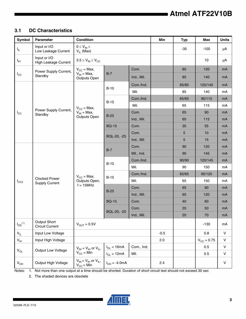
3.1 DC Characteristics
Notes: 1. Not more than one output at a time should be shorted. Duration of short circuit test should not exceed 30 sec
2. The shaded devices are obsolete
Symbol Parameter Condition Min Typ Max Units
IILInput or I/OLow Leakage Current
0 VIN VIL (Max)
-35 -100 µA
IIHInput or I/OHigh Leakage Current
3.5 VIN VCC 10 µA
ICCPower Supply Current,Standby
VCC = Max,VIN = Max,Outputs Open
B-7Com. 85 120 mA
Ind., Mil. 85 140 mA
ICCPower Supply Current,Standby
VCC = Max,VIN = Max,Outputs Open
B-10Com./Ind. 85/85 120/140 mA
Mil. 85 140 mA
B-15Com./Ind. 65/65 90/115 mA
Mil. 65 115 mA
B-25Com. 65 90 mA
Ind., Mil. 65 115 mA
BQ-15 Com. 35 55 mA
BQL-20, -25Com. 5 10 mA
Ind., Mil. 5 15 mA
ICC2Clocked PowerSupply Current
VCC = Max,Outputs Open,f = 15MHz
B-7Com. 90 120 mA
Mil., Ind. 90 145 mA
B-10Com./Ind. 90/90 120/145 mA
Mil. 90 150 mA
B-15Com./Ind. 65/65 90/120 mA
Mil. 65 150 mA
B-25Com. 65 90 mA
Ind., Mil. 65 120 mA
BQ-15 Com. 40 60 mA
BQL-20, -25Com. 20 50 mA
Ind., Mil. 20 70 mA
IOS(1) Output Short
Circuit CurrentVOUT = 0.5V -130 mA
VIL Input Low Voltage -0.5 0.8 V
VIH Input High Voltage 2.0 VCC + 0.75 V
VOL Output Low VoltageVIN = VIH or VIL,VCC = Min
IOL = 16mA Com., Ind. 0.5 V
IOL = 12mA Mil. 0.5 V
VOH Output High VoltageVIN = VIH or VIL,VCC = Min
IOH = -4.0mA 2.4 V
30250M–PLD–7/10
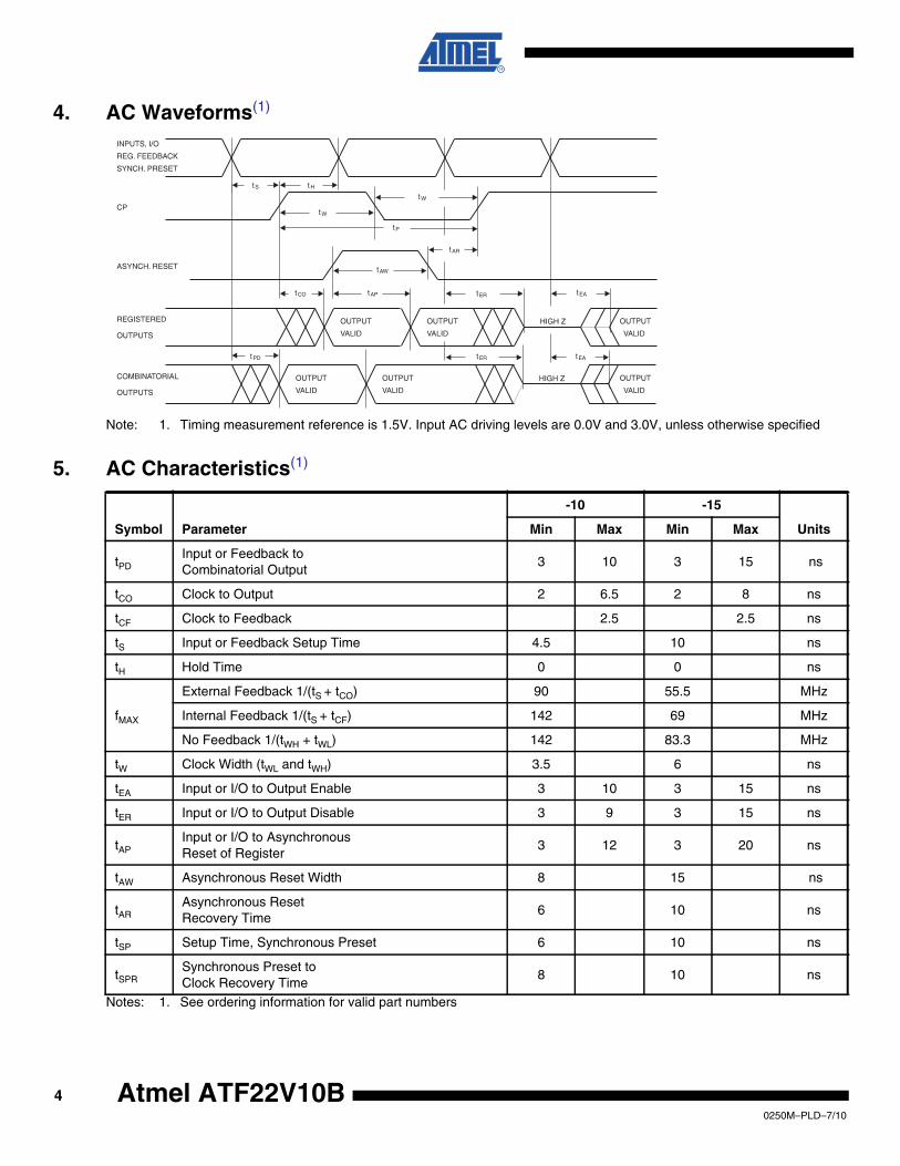
4. AC Waveforms(1)
Note: 1. Timing measurement reference is 1.5V. Input AC driving levels are 0.0V and 3.0V, unless otherwise specified
5. AC Characteristics(1)
Notes: 1. See ordering information for valid part numbers
Symbol Parameter
-10 -15
UnitsMin Max Min Max
tPDInput or Feedback toCombinatorial Output
3 10 3 15 ns
tCO Clock to Output 2 6.5 2 8 ns
tCF Clock to Feedback 2.5 2.5 ns
tS Input or Feedback Setup Time 4.5 10 ns
tH Hold Time 0 0 ns
fMAX
External Feedback 1/(tS + tCO) 90 55.5 MHz
Internal Feedback 1/(tS + tCF) 142 69 MHz
No Feedback 1/(tWH + tWL) 142 83.3 MHz
tW Clock Width (tWL and tWH) 3.5 6 ns
tEA Input or I/O to Output Enable 3 10 3 15 ns
tER Input or I/O to Output Disable 3 9 3 15 ns
tAPInput or I/O to AsynchronousReset of Register
3 12 3 20 ns
tAW Asynchronous Reset Width 8 15 ns
tARAsynchronous ResetRecovery Time
6 10 ns
tSP Setup Time, Synchronous Preset 6 10 ns
tSPRSynchronous Preset toClock Recovery Time
8 10 ns
40250M–PLD–7/10
Atmel ATF22V10B
Atmel ATF22V10B
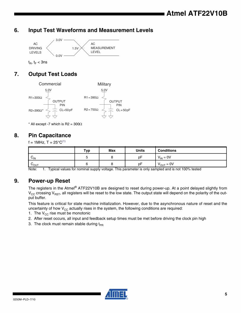
6. Input Test Waveforms and Measurement Levels
tR, tF < 3ns
7. Output Test Loads
* All except -7 which is R2 = 300
8. Pin Capacitance
Note: 1. Typical values for nominal supply voltage. This parameter is only sampled and is not 100% tested
9. Power-up ResetThe registers in the Atmel® ATF22V10B are designed to reset during power-up. At a point delayed slightly fromVCC crossing VRST, all registers will be reset to the low state. The output state will depend on the polarity of the out-put buffer.
This feature is critical for state machine initialization. However, due to the asynchronous nature of reset and theuncertainty of how VCC actually rises in the system, the following conditions are required:1. The VCC rise must be monotonic2. After reset occurs, all input and feedback setup times must be met before driving the clock pin high3. The clock must remain stable during tPR
Commercial Military
f = 1MHz, T = 25°C(1)
Typ Max Units Conditions
CIN 5 8 pF VIN = 0V
COUT 6 8 pF VOUT = 0V
50250M–PLD–7/10
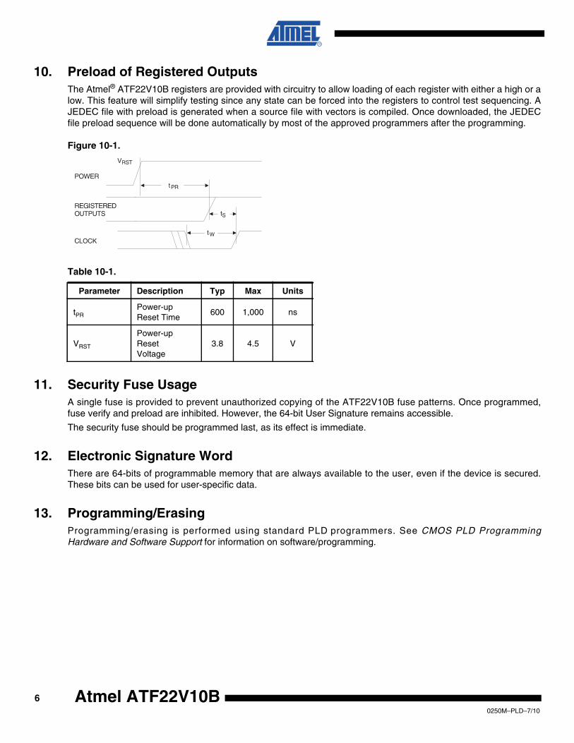
10. Preload of Registered OutputsThe Atmel® ATF22V10B registers are provided with circuitry to allow loading of each register with either a high or alow. This feature will simplify testing since any state can be forced into the registers to control test sequencing. AJEDEC file with preload is generated when a source file with vectors is compiled. Once downloaded, the JEDECfile preload sequence will be done automatically by most of the approved programmers after the programming.
Figure 10-1.
Table 10-1.
11. Security Fuse UsageA single fuse is provided to prevent unauthorized copying of the ATF22V10B fuse patterns. Once programmed,fuse verify and preload are inhibited. However, the 64-bit User Signature remains accessible.
The security fuse should be programmed last, as its effect is immediate.
12. Electronic Signature WordThere are 64-bits of programmable memory that are always available to the user, even if the device is secured.These bits can be used for user-specific data.
13. Programming/ErasingProgramming/erasing is performed using standard PLD programmers. See CMOS PLD ProgrammingHardware and Software Support for information on software/programming.
Parameter Description Typ Max Units
tPRPower-upReset Time
600 1,000 ns
VRST
Power-upResetVoltage
3.8 4.5 V
60250M–PLD–7/10
Atmel ATF22V10B
Atmel ATF22V10B
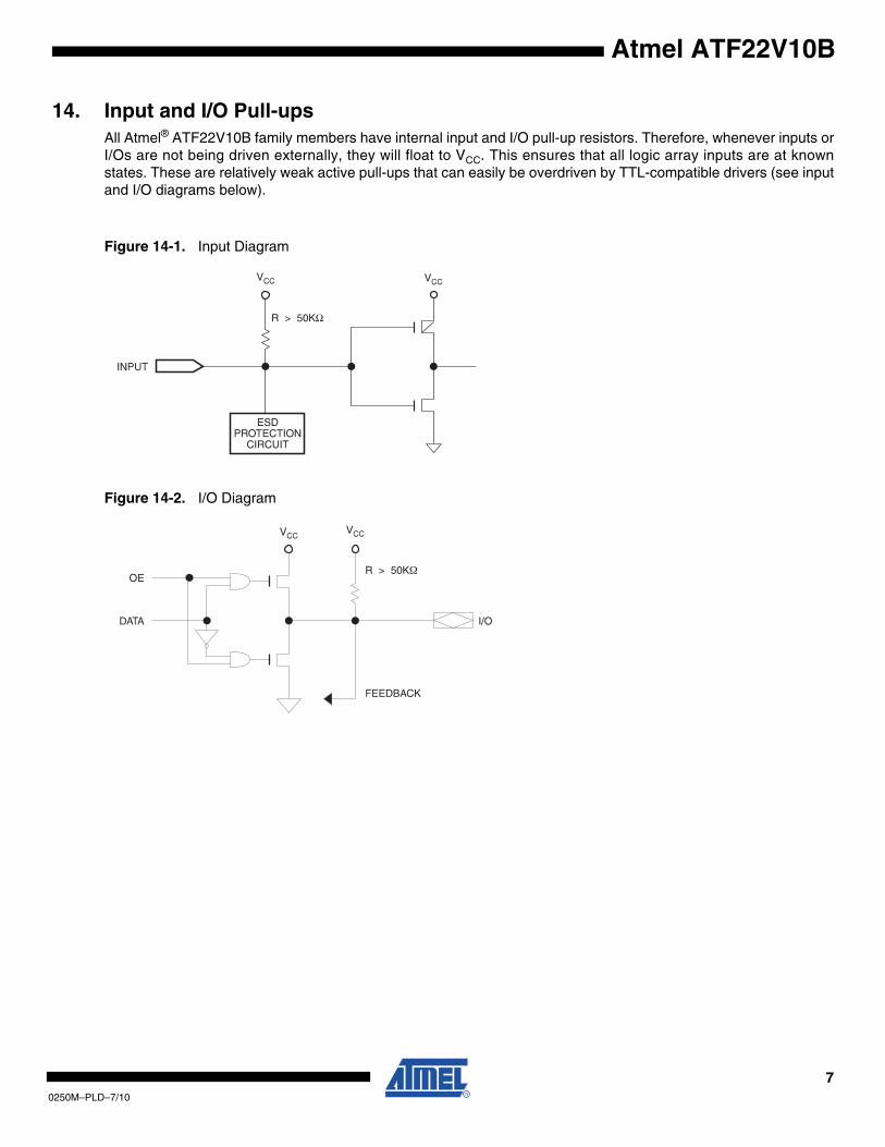
14. Input and I/O Pull-upsAll Atmel® ATF22V10B family members have internal input and I/O pull-up resistors. Therefore, whenever inputs orI/Os are not being driven externally, they will float to VCC. This ensures that all logic array inputs are at knownstates. These are relatively weak active pull-ups that can easily be overdriven by TTL-compatible drivers (see inputand I/O diagrams below).
Figure 14-1. Input Diagram
Figure 14-2. I/O Diagram
70250M–PLD–7/10
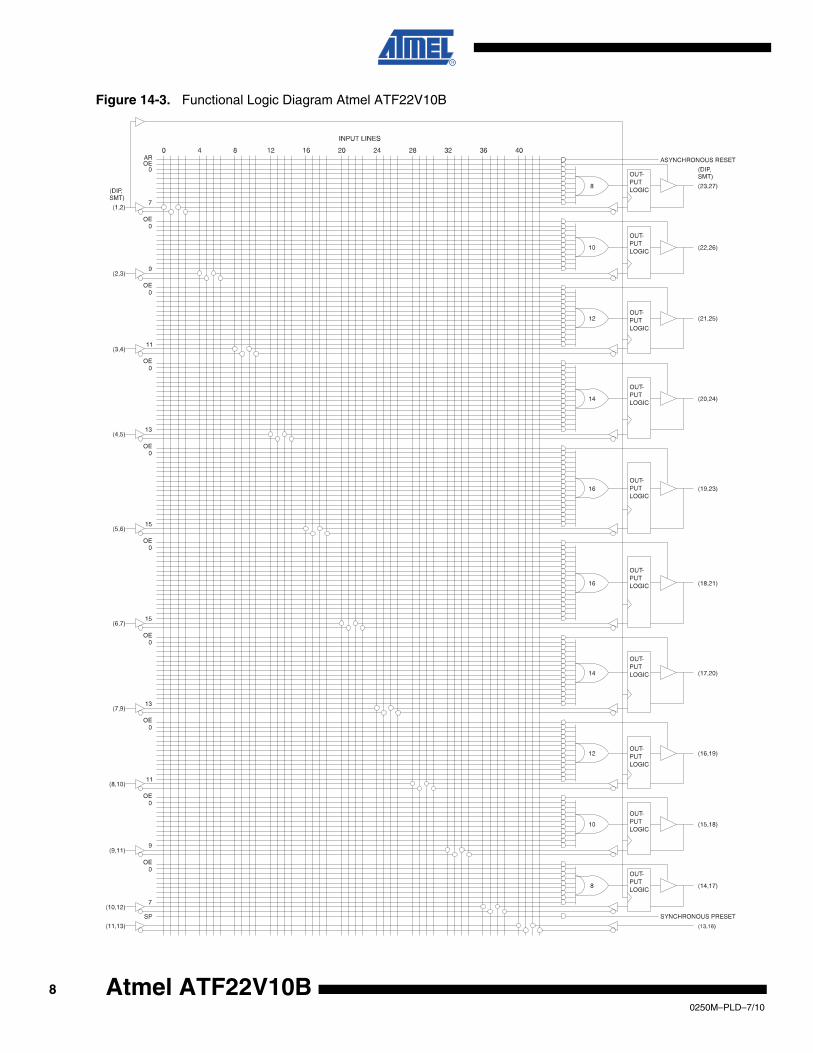
Figure 14-3. Functional Logic Diagram Atmel ATF22V10B
80250M–PLD–7/10
Atmel ATF22V10B
Atmel ATF22V10B
ATMEL ATMEL
ATMELATMEL
ATMEL ATMEL
90250M–PLD–7/10
100250M–PLD–7/10
Atmel ATF22V10B
Atmel ATF22V10B
110250M–PLD–7/10
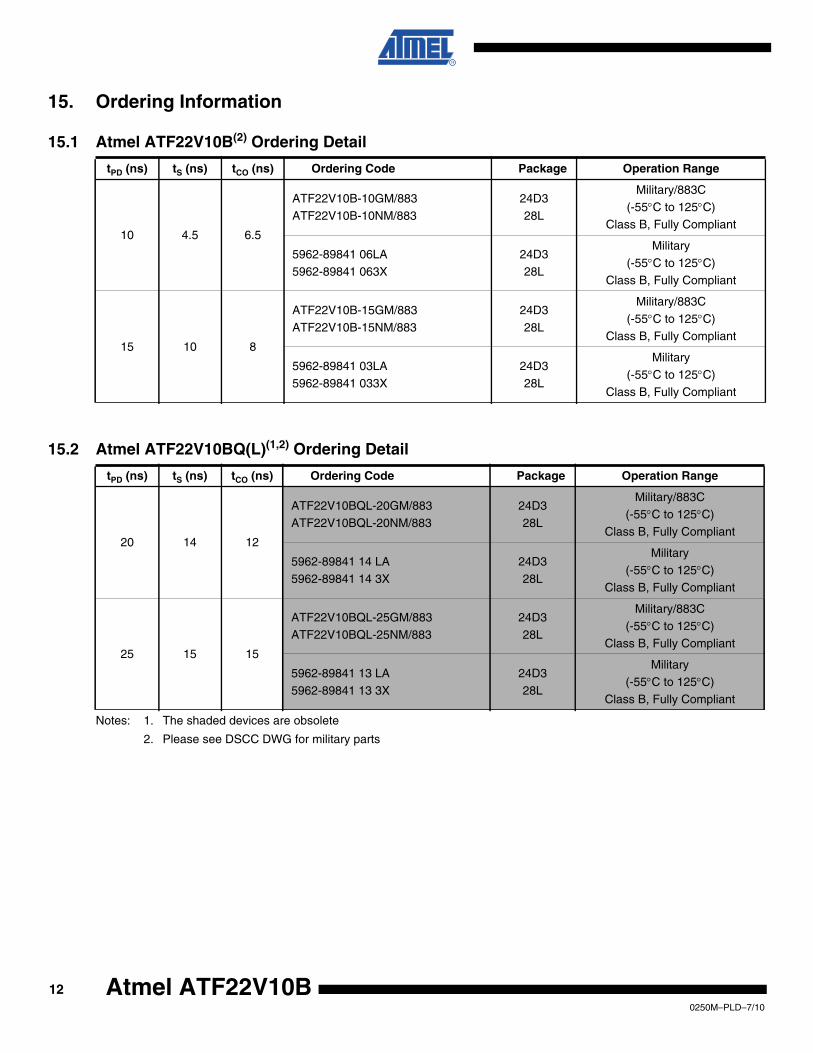
15. Ordering Information
15.1 Atmel ATF22V10B(2) Ordering Detail
15.2 Atmel ATF22V10BQ(L)(1,2) Ordering Detail
Notes: 1. The shaded devices are obsolete
2. Please see DSCC DWG for military parts
tPD (ns) tS (ns) tCO (ns) Ordering Code Package Operation Range
10 4.5 6.5
ATF22V10B-10GM/883ATF22V10B-10NM/883
24D328L
Military/883C(-55C to 125C)
Class B, Fully Compliant
5962-89841 06LA5962-89841 063X
24D328L
Military(-55C to 125C)
Class B, Fully Compliant
15 10 8
ATF22V10B-15GM/883ATF22V10B-15NM/883
24D328L
Military/883C(-55C to 125C)
Class B, Fully Compliant
5962-89841 03LA5962-89841 033X
24D328L
Military(-55C to 125C)
Class B, Fully Compliant
tPD (ns) tS (ns) tCO (ns) Ordering Code Package Operation Range
20 14 12
ATF22V10BQL-20GM/883ATF22V10BQL-20NM/883
24D328L
Military/883C(-55C to 125C)
Class B, Fully Compliant
5962-89841 14 LA5962-89841 14 3X
24D328L
Military(-55C to 125C)
Class B, Fully Compliant
25 15 15
ATF22V10BQL-25GM/883ATF22V10BQL-25NM/883
24D328L
Military/883C(-55C to 125C)
Class B, Fully Compliant
5962-89841 13 LA5962-89841 13 3X
24D328L
Military(-55C to 125C)
Class B, Fully Compliant
120250M–PLD–7/10
Atmel ATF22V10B

Atmel ATF22V10B
16. Packaging Information
24D324D3, 24-lead, 0.300"Wide. Non-windowed,Ceramic Dual Inline Parkage (Cerdip)Dimensions in Millimeters and (Inches)*MIL-STD-1835 D-9 CONFIG A (Glass Sealed)
*Controlling dimension: Inches
REV. A 04/11/2001
130250M–PLD–7/10
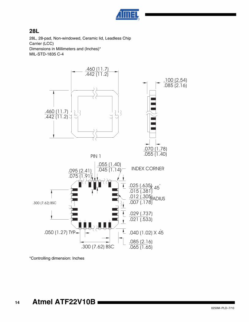
28L28L, 28-pad, Non-windowed, Ceramic lid, Leadless ChipCarrier (LCC)Dimensions in Millimeters and (Inches)*MIL-STD-1835 C-4
*Controlling dimension: Inches
140250M–PLD–7/10
Atmel ATF22V10B
Atmel ATF22V10B
17. Revision History
Doc. Rev. Date Comments
0250M 07/2010 Removed all commerical and industrial grade leaded part offerings
150250M–PLD–7/10
0250M–PLD–7/10
Headquarters International
Atmel Corporation2325 Orchard ParkwaySan Jose, CA 95131USATel: (+1)(408) 441-0311Fax: (+1)(408) 487-2600www.atmel.com
Atmel Asia LimitedUnit 01-5 & 16, 19/FBEA Tower, Millennium City 5418 Kwun Tong RoadKwun Tong, KowloonHONG KONGTel: (+852) 2245-6100Fax: (+852) 2722-1369
Atmel Munich GmbHBusiness CampusParkring 4D-85748 Garching b. MunichGERMANYTel: (+49) 89-31970-0Fax: (+49) 89-3194621
Atmel Japan9F, Tonetsu Shinkawa Bldg.1-24-8 ShinkawaChuo-ku, Tokyo 104-0033JAPANTel: (+81) 3-3523-3551Fax: (+81) 3-3523-7581
Product Contact
Technical [email protected]
Sales Contactwww.atmel.com/contacts
Literature Requestswww.atmel.com/literature
Disclaimer: The information in this document is provided in connection with Atmel products. No license, express or implied, by estoppel or otherwise, to anyintellectual property right is granted by this document or in connection with the sale of Atmel products. EXCEPT AS SET FORTH IN ATMEL’S TERMS AND CONDI-TIONS OF SALE LOCATED ON ATMEL’S WEB SITE, ATMEL ASSUMES NO LIABILITY WHATSOEVER AND DISCLAIMS ANY EXPRESS, IMPLIED OR STATUTORYWARRANTY RELATING TO ITS PRODUCTS INCLUDING, BUT NOT LIMITED TO, THE IMPLIED WARRANTY OF MERCHANTABILITY, FITNESS FOR A PARTICULARPURPOSE, OR NON-INFRINGEMENT. IN NO EVENT SHALL ATMEL BE LIABLE FOR ANY DIRECT, INDIRECT, CONSEQUENTIAL, PUNITIVE, SPECIAL OR INCIDEN-TAL DAMAGES (INCLUDING, WITHOUT LIMITATION, DAMAGES FOR LOSS OF PROFITS, BUSINESS INTERRUPTION, OR LOSS OF INFORMATION) ARISING OUT OFTHE USE OR INABILITY TO USE THIS DOCUMENT, EVEN IF ATMEL HAS BEEN ADVISED OF THE POSSIBILITY OF SUCH DAMAGES. Atmel makes norepresentations or warranties with respect to the accuracy or completeness of the contents of this document and reserves the right to make changes to specificationsand product descriptions at any time without notice. Atmel does not make any commitment to update the information contained herein. Unless specifically providedotherwise, Atmel products are not suitable for, and shall not be used in, automotive applications. Atmel’s products are not intended, authorized, or warranted for useas components in applications intended to support or sustain life.
© 2010 Atmel Corporation. All rights reserved.Atmel®, Atmel logo and combinations thereof and others are registered trademarks or trademarks of Atmel Corporation or its subsidiaries. Otherterms and product names may be trademarks of others.