Embed Size (px)
Citation preview
Journal of Microelectronics and Electronic Packaging (2017) 14, 132-139Copyright © International Microelectronics Assembly and Packaging SocietyISSN: 1551-4897
Localized Laser Sintering of Metal Nanoparticle Inks Printedwith Aerosol Jet® Technology for Flexible Electronics
Michael J. Renn, Matthew Schrandt, Jaxon Renn, and James Q. Feng*
Abstract—Direct-write methods, such as the Aerosol Jet®technology, have enabled fabrication of flexible multifunctional 3-Ddevices by printing electronic circuits on thermoplastic and ther-moset polymer materials. Conductive traces printed by additivemanufacturing typically start in the form of liquid metal nano-particle inks. To produce functional circuits, the printed metalnanoparticle ink material must be postprocessed to form con-ductive metal by sintering at elevated temperature. Metal nano-particles are widely used in conductive inks because they can besintered at relatively low temperatures compared with the meltingtemperature of bulk metal. This is desirable for fabricating circuitson low-cost plastic substrates. To minimize thermal damage to theplastics, while effectively sintering the metal nanoparticle inks, wedescribe a laser sintering process that generates a localized heat-affected zone (HAZ) when scanning over a printed feature. Forsintering metal nanoparticles that are reactive to oxygen, an inertor reducing gas shroud is applied around the laser spot to shield theHAZ from ambient oxygen. With the shroud gas-shielded laser,oxygen-sensitive nanoparticles, such as those made of copper andnickel, can be successfully sintered in open air. With very shortheating time and small HAZ, the localized peak sintering tem-perature can be substantially higher than that of damage thresholdfor the underlying substrate, for effective metallization of nano-particle inks. Here, we demonstrate capabilities for producingconductive tracks of silver, copper, and copper–nickel alloys onflexible films as well as fabricating functional thermocouples andstrain gauge sensors, with printed metal nanoparticle inks sinteredby shroud-gas-shielded laser.
Keywords—Printed electronics, laser sintering, metal nano-particle ink
INTRODUCTION
To fabricate electronic circuits on flexible substrates ofcomplex shapes, the approach of printing metal nano-
particle inks directly onto substrate followed by a postprocessmetallization step has become increasingly popular for low-costmanufacturing [1]. With the Aerosol Jet® direct-write tech-nology, the “ink” is deposited in a form of high-speed collimatedjet of aerosol droplets through an aerodynamic focusing nozzlewith sheath gas. Microscale high-aspect-ratio features of variousmaterials can be conformally printed onto substrates of complexgeometries. This makes the Aerosol Jet® technology attractiveto numerous applications, such as printed electronics, printed
sensors, to mention a few [2-4]. Its capability of noncontactconformal printing of metal nanoparticle inks and non-conductive polymer materials can be used to create electroniccircuits in a variety of novel form-factors, for fabricatingmultifunctional 3-D devices.
But metal nanoparticle inks typically contain organic stabi-lizers (dispersants for preventing nanoparticle agglomeration inliquid solvent) and they do not become conductive with dryingalone. The organic components must be removed and electricalcontacts must be established between metal nanoparticles beforeuseful conductivity can be achieved. The organic componentremoval and nanoparticle contact enhancement can be effec-tively accomplished at an elevated temperature, where polymersare eliminated by thermal decomposition–vaporization and thenanoparticles are fused via interparticle atomic diffusion.
Sintering metal nanoparticle inks has recently become anintensive research subject because of the growing interest indirect metallization with printed electronics, to replace themultistep, much more complicated lithographic processes usedin traditional electronics production. Many sintering tech-niques have been developed with various levels of success.The simplest and most commonly used method is to heat theentire printed parts in a thermal oven. Depending on the inkformulation and nanoparticle size, the temperature for ovensintering is in the range from 120°C to 250°C, much lower thanthe corresponding bulk metal melting point. The melting pointof nanoparticles is lowered by virtue of thermodynamic sizeeffect associated with their large surface energy (known as“melting point depression”) [5]. When heated in an oven, manylow-cost polymeric substrates with Tg close to the sinteringtemperature would suffer extensive thermal damage. More-over, sintering in an oven with restricted temperature oftentakes hours. Such an extended heating makes oven sintering ofoxygen-sensitive materials (e.g., copper and nickel) imprac-tical under the ambient atmosphere. Copper nanoparticle inksare attractive for printed electronics because of its superiorconductivity and low cost of raw materials. Although usingoven sintering in vacuum or inert/reducing gas environmentcan mitigate the copper oxidation problem, it also eliminates itslow cost advantage because expensive high-temperatureplastic substrates must be used. Among several alternativetechniques, rapid localized laser sintering offers the mostdesirable attributes, such as a small spot size for minimizingheat-affected zone (HAZ), while delivering adequate heatingin a short duration, to enable sintering on temperature-sensitivesubstrates and to prevent extensive oxidation of oxygen-sensitive metals.
The manuscript was received on August 30, 2017; revision received onOctober 18, 2017; accepted on October 19, 2017
Optomec Inc., 2575 University Ave, #135, St Paul, Minnesota*Corresponding author; email: [email protected]
doi:10.4071/imaps.521797 1551-4897 © 2017 International Microelectronics Assembly and Packaging Society
Promising results of laser sintering of metal nanoparticle inkshave been reported by many authors, mostly with ink layers ofthickness below one micron (i.e., <1,000 nm) [6-11]. Unlikeinkjet printing which operates with larger droplets of low vis-cosity inks, the Aerosol Jet® printed lines can have a muchhigher aspect ratio (with layer thickness typically of severalmicrons as printed in a single pass) because of the effective in-flight solvent removal with microdroplets of appropriatelyformulated inks [12]. For the same area of line cross-section,which determines the line conductance, the Aerosol Jet® printedlines can be much narrower, enabling production of higherdensity electronic circuitry. Sintering high-aspect-ratio lines canpose technical challenges with respect to crack formation [9] andmaterial delamination (because of high pressure gas pocketformation) [11].In this work, we present a shroud-gas-shielded laser sintering
process of metal nanoparticle inks for producing conductivetracks of silver, copper, and copper–nickel alloys on flexiblefilms, thermocouples, and strain gauges printed with the AerosolJet® direct-write technology. Challenges related to robustprocessing and scaling to production are also discussed.
METHODS
As is typical with printed electronics, metal nanoparticle (NP)inks are first deposited on a substrate by a printing process, andthen sintered at an elevated temperature. In the present work, theAerosol Jet® direct-write technology is used for printing, andthen a high-power laser beam is used for localized sintering as itmoves at a variable speed along the same toolpath as that forprinting. By adjusting the laser power and scan speed, the localheating temperature and duration can be effectively controlled.To avoid thermal damage to temperature-sensitive substrate, it isimportant to restrict the heating duration to a time scale ofmilliseconds such that the metallization is accomplished beforethe thermal diffusion front penetrates too deeply into the sub-strate. A shroud-gas shield around the laser HAZ inhibits ox-idation of sensitive metal NP inks, such as Cu, Ni, and Cu–Nialloys [13].
A. Aerosol Jet® System
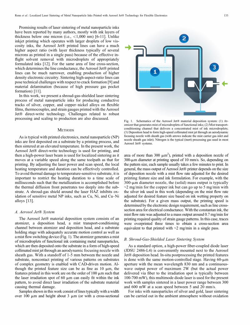
The Aerosol Jet® material deposition system consists of anatomizer, a deposition head, a mist transport-conditioningchannel between atomizer and deposition head, and a substrateholding stage with adequately accurate motion control as well asamist flow switching device (Fig. 1). The atomizer generates amistof microdroplets of functional ink containing metal nanoparticles,which are then deposited onto the substrate in a form of high-speedcollimatedmist jet through an aerodynamic focusing nozzle withsheath gas. With a standoff of 1-5 mm between the nozzle andsubstrate, noncontact printing of various patterns on substratesof complex geometry is enabled with CAD-driven motion. Al-though the printed feature size can be as fine as 10 mm, thefeatures printed in this work are on the order of 100 mm such thatthe laser irradiation spot of 60 mm can easily fit within the inkpattern, to avoid direct laser irradiation of the substrate materialcausing thermal damage.Samples shown in thiswork consist of lines typicallywith awidth
over 100 mm and height about 3 mm (or with a cross-sectional
area of more than 300 mm2), printed with a deposition nozzle of300-mm diameter at printing speed of 10 mm/s. So, depending onthe pattern size, each sample usually takes a fewminutes to print. Ingeneral, the mass output of Aerosol Jet® printer depends on the sizeof deposition nozzle with a mist flow rate adjusted for the desiredprinting feature size and ink formulation. For example, with the300-mm diameter nozzle, the (solid) mass output is typically~2 mg/min for the copper ink but can go up to 5 mg/min withthe silver ink used in this work (depending on the mist flow rateadjusted for desired feature size based on ink wetting property onthe substrate). For a given mass output, the printing speed isdetermined by the electronic design requirement, such as line cross-section area for electrical conductance.With the constantan ink, themist flow rate was adjusted to a mass output around 0.7 mg/min forprinting required quality of strain gauge patterns. In this case, traceswere overprinted three times to obtain a cross-section areaequivalent to that printed with ~2 mg/min in a single pass.
B. Shroud-Gas-Shielded Laser Sintering System
As a standard option, a high-power fiber-coupled diode laser(JDSU 2486-L4) is conveniently mounted next to the AerosolJet® deposition head. In-situ postprocessing the printed featuresis done with the same motion-controlled stage. Having 60-mmaperture with the mean wavelength 830 nm and a continuous-wave output power of maximum 2W (but the actual powerdelivered via fiber to the irradiation spot is typically between100-700 mW), this multimode diode laser is used for the presentwork with samples sintered in a laser power range between 300and 600 mW at a scan speed between 5 and 20 mm/s.
For inks with nanoparticles of silver and gold, laser sinteringcan be carried out in the ambient atmosphere without oxidation
Fig. 1. Schematics of the Aerosol Jet® material deposition system: (1) At-omizer that generates mist of microdroplets of functional inks; (2)Mist transport-conditioning channel that delivers a concentrated mist of ink microdroplets;(3) Deposition head to form high-speed collimated mist jet through an aerodynamicfocusing nozzle with sheath gas (with arrows indicate the mist carrier gas inlet andnozzle sheath gas inlet). Nitrogen is the typical (inert) processing gas used in mostAerosol Jet® systems.
Renn et al.: Localized Laser Sintering of Metal Nanoparticle Inks Printed with Aerosol Jet® Technology for Flexible Electronics 133
degradation because of high free energies of their oxides.Despite its high conductivity and oxidation resistance, silver iscostly and does not have great mechanical strength. Silver is alsoknown to be prone to electromigration that can cause failure ofcircuit functionality and is not easy to solder on. Copper, on theother hand, is intrinsically less susceptible to electromigrationand relatively low cost because of its abundant availability.Copper is also known to have excellent conductivity, goodmechanical strength, and easy for soldering. But copper tends tobe oxidized when sintering at elevated temperature in ambientatmosphere.
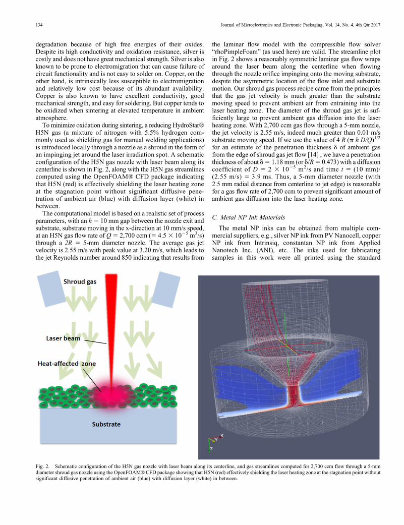
To minimize oxidation during sintering, a reducing HydroStar®H5N gas (a mixture of nitrogen with 5.5% hydrogen com-monly used as shielding gas for manual welding applications)is introduced locally through a nozzle as a shroud in the form ofan impinging jet around the laser irradiation spot. A schematicconfiguration of the H5N gas nozzle with laser beam along itscenterline is shown in Fig. 2, along with the H5N gas streamlinescomputed using the OpenFOAM® CFD package indicatingthat H5N (red) is effectively shielding the laser heating zoneat the stagnation point without significant diffusive pene-tration of ambient air (blue) with diffusion layer (white) inbetween.
The computational model is based on a realistic set of processparameters, with an h5 10 mm gap between the nozzle exit andsubstrate, substrate moving in the x-direction at 10 mm/s speed,at an H5N gas flow rate of Q5 2,700 ccm (5 4.53 1025 m3/s)through a 2R 5 5-mm diameter nozzle. The average gas jetvelocity is 2.55 m/s with peak value at 3.20 m/s, which leads tothe jet Reynolds number around 850 indicating that results from
the laminar flow model with the compressible flow solver“rhoPimpleFoam” (as used here) are valid. The streamline plotin Fig. 2 shows a reasonably symmetric laminar gas flow wrapsaround the laser beam along the centerline when flowingthrough the nozzle orifice impinging onto the moving substrate,despite the asymmetric location of the flow inlet and substratemotion. Our shroud gas process recipe came from the principlesthat the gas jet velocity is much greater than the substratemoving speed to prevent ambient air from entraining into thelaser heating zone. The diameter of the shroud gas jet is suf-ficiently large to prevent ambient gas diffusion into the laserheating zone. With 2,700 ccm gas flow through a 5-mm nozzle,the jet velocity is 2.55 m/s, indeed much greater than 0.01 m/ssubstrate moving speed. If we use the value of 4 R (p h D/Q)1/2
for an estimate of the penetration thickness d of ambient gasfrom the edge of shroud gas jet flow [14] , we have a penetrationthickness of about d5 1.18mm (or d/R5 0.473) with a diffusioncoefficient of D 5 2 3 1025 m2/s and time t 5 (10 mm)/(2.55 m/s) 5 3.9 ms. Thus, a 5-mm diameter nozzle (with2.5 mm radial distance from centerline to jet edge) is reasonablefor a gas flow rate of 2,700 ccm to prevent significant amount ofambient gas diffusion into the laser heating zone.
C. Metal NP Ink Materials
The metal NP inks can be obtained from multiple com-mercial suppliers, e.g., silver NP ink from PVNanocell, copperNP ink from Intrinsiq, constantan NP ink from AppliedNanotech Inc. (ANI), etc. The inks used for fabricatingsamples in this work were all printed using the standard
Fig. 2. Schematic configuration of the H5N gas nozzle with laser beam along its centerline, and gas streamlines computed for 2,700 ccm flow through a 5-mmdiameter shroud gas nozzle using the OpenFOAM®CFD package showing that H5N (red) effectively shielding the laser heating zone at the stagnation point withoutsignificant diffusive penetration of ambient air (blue) with diffusion layer (white) in between.
134 Journal of Microelectronics and Electronic Packaging, Vol. 14, No. 4, 4th Qtr 2017
pneumatic atomizer that came with the Aerosol Jet® systemwith equipped virtual impactor for adjusting the mist flow rateto the deposition nozzle.Table I shows that Ag has the best electrical conductivity, but
does not offer good mechanical strength. The mechanicalstrength of Cu and Ni are much better than Ag, with electricalconductivity of Cu very close to that of Ag. On the other hand,Cu and Ni have good solderability that is usually lacking withAg, and they are less susceptible to electromigration than Ag.The large temperature coefficient of resistance (TCR) of Nicombining with its high resistivity makes Ni a good material formaking thermistors. The exceptionally low magnitude of theTCR of constantan (a Cu55Ni45 alloy) makes it attractive formany sensor applications when the signal sensitivity to temperature
variation is undesirable. The large magnitude of Seebeckcoefficient of constantan also makes it attractive for makingthermocouples and applications in energy harvesting. Al-though Au has good electrical conductivity and large yieldstrength, it is cost-prohibitive in most applications. The silverpolymer thick film (Ag PTF, which has Ag flakes imbedded inan elastomer) ink offers very high elongation that is attractivefor flexible circuit applications, but it also has a much lowerelectrical conductivity compared with most of the metal NPinks.
It should be noted that the “sintering T” in thermal ovengiven in Table I only serves as a convenient reference value,which usually depends on the NP size as well as the dispersanttype and solvents of a particular ink and can vary in a wide
Table IMetal Material Properties and Typical Metal NP Ink Sintering Temperature in Thermal Oven
Material Resistivity (mV cm) TCR (K-1) Yield strength (MPa) Elongation (%) Seebeck coeff. (mV/K) Sintering T (°C)
Silver (Ag) 1.6 3.8E-3 55 35 6.5 120Gold (Au) 2.4 3.4E-3 205 45 6.5 200Copper (Cu) 1.7 3.9E-3 117 40 6.5 220Nickel (Ni) 7.0 5.8E-3 140-350 40 215 350Cu55Ni45 49.0 27.4E-5 140 45 235 400Ag PTF 1,000 1001 170
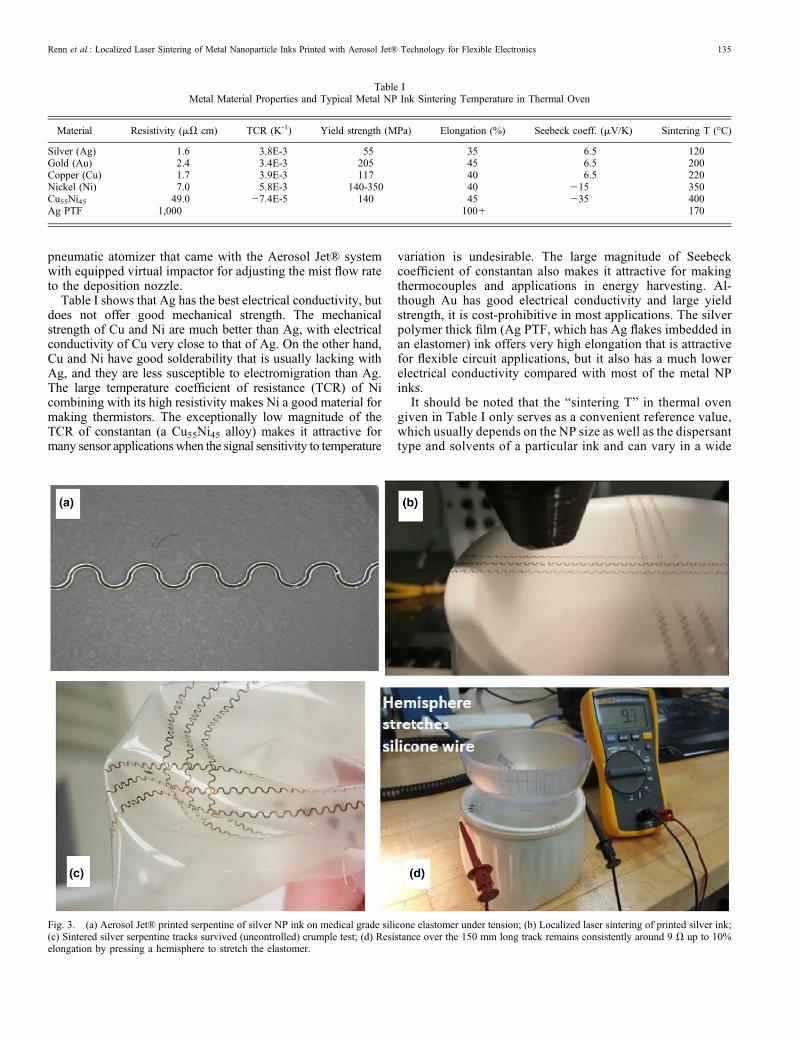
Fig. 3. (a) Aerosol Jet® printed serpentine of silver NP ink on medical grade silicone elastomer under tension; (b) Localized laser sintering of printed silver ink;(c) Sintered silver serpentine tracks survived (uncontrolled) crumple test; (d) Resistance over the 150 mm long track remains consistently around 9 V up to 10%elongation by pressing a hemisphere to stretch the elastomer.
Renn et al.: Localized Laser Sintering of Metal Nanoparticle Inks Printed with Aerosol Jet® Technology for Flexible Electronics 135
range. For example, the value “120” for silver NP ink ac-tually came from that of PV Nanocell specifically used in thiswork (with NP diameters about 80 nm); there are many othersilver NP inks often requiring higher oven sintering temper-ature (e.g., 150°C or even higher) for adequate conductivity,adhesion, etc.
RESULTS
The primary advantage of laser sintering are to enableprinting electronic circuits on temperature sensitive sub-strates which would be susceptible to thermal damage whensintered in a thermal oven. Even with substrate materials thatcan withstand high temperature, the mismatch of thermalexpansion behavior can cause printed traces to crack anddelaminate when sintered in an oven for extended durations.Using localized laser irradiation, we have successful sinteredmetal NP ink on an acrylic plastic (Tg ~ 100°C) and PETpolymer film (Tg ~ 80°C). These materials would warp ina thermal oven at temperature approaching their Tg values. Toavoid cracking caused by extensive thermal expansion ofa substrate, we show the possibility of using a localized lasersintering to fabricate conductive sliver tracks on flexiblemedical grade silicone elastomer. With the inert and/or re-ducing shroud gas of HydroStar H5N shielding around thelocalized laser heating zone, successful sintering of copperand nickel inks for fabricating thermocouples and straingauges are also demonstrated.
A. Silver NP Ink on Silicone Elastomer
To sinter silver NP ink on temperature-sensitive materials(such as acrylic glass, PET film, etc.) without serious thermaldamage to the substrate, the localized heating process needs tobe carefully controlled. The key for success is to have suffi-ciently high laser power for effective sintering of the metal NP
ink quickly within a short irradiation duration such that thethermal diffusion front cannot penetrate too deeply into thesubstrate before the laser irradiation is moved away. The sameprinciple can be applied to sintering the metal NP ink on flexiblesubstrates of elastomers, such as silicone. Although silicone canwithstand higher temperature, its extensive thermal expansiontends to result in cracking and delamination of printed metal NPtracks that usually shrink during sintering at an elevated temper-ature. With localized laser sintering, the silicone thermal expansioncan be limited in a small heat-affected zone, so the printed con-ductive tracks can be fabricated without cracking and delaminationdue to otherwise extensive thermal expansion of the substrate.
To demonstrate such an advantage of laser sintering, flexibleconductive tracks consisting of silver ink serpentines are printedand sintered with localized laser irradiation on a medical gradesilicone elastomer substrate. As shown in Fig. 3, those con-ductive tracks can remain conductive through crumple andstretch tests up to 10% elongation. In this case, the conductivetracks of ~200 mm wide and ~4 mm high were printed witha (solid) mass output of ~5 mg/min. With measured 9 V re-sistance over a 150 mm track of ~750 mm2 cross-section area,we can derive a resistivity of 4.5 mV cm which is about threetimes that of bulk silver (i.e., 1.6 mV cm).
B. Thermocouples Printed with Copper and Copper–NickelAlloy NP Inks
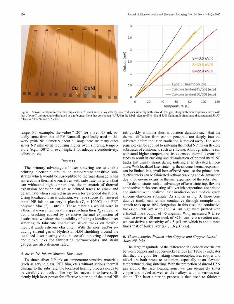
The large magnitude of the difference in Seebeck coefficientbetween copper and copper–nickel alloys (in Table I) indicatesthat they are good for making thermocouples. But copper andnickel are both prone to oxidation, especially at an elevatedtemperature during sintering.With the protection of shroud H5Ngas around the laser heating zone, we can adequately sintercopper and nickel as well as their alloys without serious oxi-dation. The laser sintering process is then used to fabricate
Fig. 4. Aerosol Jet® printed thermocouples with Cu and Cu–Ni alloy inks by localized laser sintering with shroud H5N gas, along with their response curves withthat of type T thermocouple displayed as a reference. Note that constantan [45/55] in the label refers to 45% Ni and 55% Cu in mole fraction and constantan [50/50]refers to 50% Ni and 50% Cu.
136 Journal of Microelectronics and Electronic Packaging, Vol. 14, No. 4, 4th Qtr 2017

thermocouples using copper and copper–nickel alloy inks asshown in Fig. 4. The response curves of those thermocouplesshow their reasonable functionality and that of the printedcopper-constantan thermocouple is comparable to the com-mercial type T thermocouple.
C. Strain Gauges Printed with Constantan NP Ink
With its low temperature coefficient of resistance and highstrain sensitivity (or gauge factor) as well as relatively highresistivity and elongation capability, constantan (Cu55Ni45) hasbecome the popular choice of material for strain gauge appli-cations. Using localized laser sintering with H5N gas shroud, theAerosol Jet® printed Wheatstone bridge circuits of constantanon a Kapton film (Fig. 5) are shown to be fully functional forstrain gauge applications. There is no signal degradation duringa cyclic bending test on a 60-mm diameter pipe with a 0.3%strain over more than 10,000 cycles.
DISCUSSIONS
With the promising proof-of-concept results of laser sinteringof Aerosol Jet® printed high aspect-ratio tracks of metalnanoparticle inks are demonstrated here [15], in-depth in-vestigations of aspects relevant to reliable production of flexibleelectronic circuits are required to optimize this technology. Forexample, the high-power fiber-coupled diode laser has beenused here only because of its availability in our laboratory; othertypes of lasers with different wavelengths and spot sizes can beacquired from different vendors for investigations of effects oflaser wavelength and relative spot size on laser sintering out-comes. The HydroStar® H5N (with hydrogen as the reducingcomponent) gas used for shielding the laser heating zone isshown to be effective for preventing oxidation of copper andnickel NPs during sintering, but a simpler inert shroud gas, suchas pure nitrogen, might be just as effective, which should beexplored in future work.
Fig. 5. Aerosol Jet® printed Wheatstone bridge circuit with constantan ink on 0.005” Kapton film, sintered with localized laser irradiation with shroud H5N gas.
Renn et al.: Localized Laser Sintering of Metal Nanoparticle Inks Printed with Aerosol Jet® Technology for Flexible Electronics 137
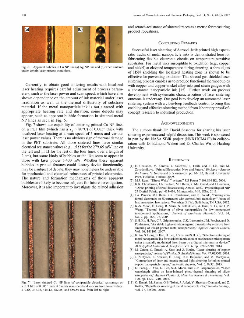
Currently, to obtain good sintering results with localizedlaser heating requires careful adjustment of process param-eters, such as the laser power and scan speed, which have alsoshown dependence on the amount of ink material under laserirradiation as well as the thermal diffusivity of substratematerial. If the metal nanoparticle ink is not sintered withappropriate heating rate and duration, some defects mayappear, such as apparent bubble formation in sintered metalNP lines as seen in Fig. 6.
Fig. 7 shows our capability of sintering printed Cu NP lineson a PET film (which has a Tg ~ 80°C) of 0.005” thick withlocalized laser heating at a scan speed of 5 mm/s and variouslaser power values. There is no obvious sign of thermal damagein the PET substrate. All those sintered lines have similarelectrical resistance values (e.g., 15V for the 279.65 mW line onthe left and 11 V for the rest of the four lines, over a length of2 cm), but some kinds of bubbles or the like seem to appear inthose with laser power >400 mW. Whether these apparentbubbles in printed features could destroy device functionalitymay be a subject of debate; they may nonetheless be undesirablefor mechanical and electrical robustness of printed electronics.The nature and formation mechanisms of those apparentbubbles are likely to become subjects for future investigation.Moreover, it is also important to investigate the related adhesion
and scratch-resistance of sintered traces as a metric for measuringproduct robustness.
CONCLUDING REMARKS
Successful laser sintering of Aerosol Jet® printed high aspect-ratio tracks of metal nanoparticle inks is demonstrated here forfabricating flexible electronic circuits on temperature sensitivesubstrates. For metal inks susceptible to oxidation (e.g., copperand nickel) at elevated temperature during sintering, a shroud gasof H5N shielding the localized heating zone is shown to beeffective for preventing oxidation. This shroud-gas-shielded lasersintering process enables us to produce functional thermocoupleswith copper and copper–nickel alloy inks and strain gauges witha constantan nanoparticle ink [15]. Further work on processdevelopment with systematic characterization of laser sinteringoutcome is underway. Our goal is to develop an automated lasersintering system with a close-loop feedback control to bring thisenabling and effective sintering method from laboratory proof-of-concept research to industrial production.
ACKNOWLEDGMENTS
The authors thank Dr. David Sessoms for sharing his lasersintering experience and helpful discussion. This work is sponsoredin part by the NASA SBIR project (NNX17CM41P) in collabo-ration with Dr Edmond Wilson and Dr Charles Wu of HardingUniversity.
REFERENCES
[1] E. Coatanea, V. Kantola, J. Kulovesi, L. Lahti, and R. Lin, and M.Zavodchikova, “Printed Electronics, Now and Future,” Bit Bang – Rays tothe Future, Y. Neuvo and S. Ylonen eds., pp. 63-102, Helsinki UniversityPrint, Helsinki, Finland, 2009.
[2] M.J. Renn, “Direct WriteTM system,” US Patent 7,108,894 B2, 2006.[3] K.K. Christenson, J.A. Paulsen, M.J. Renn, K. McDonald, and J. Bourassa,
“Direct printing of circuit boards using Aerosol Jet®,” Proceedings of NIP27 Digital Fabric, pp. 433-436, Minneapolis, MN, USA, 2011.
[4] J.A. Paulsen, M.J. Renn, K.K. Christenson, and R. Plourde, “Printing con-formal electronics on 3D structures with Aerosol Jet® technology,” Future ofInstrumentation International Workshop (FIIW), Gatlinburg, TN, USA, 2012.
[5] K.-S. Moon, H. Dong, R. Maric, S. Pothukuchi, A. Hunt, Y. Li, and C.P.Wang, “Thermal behavior of silver nanoparticles for low-temperatureinterconnect applications,” Journal of Electronic Materials, Vol. 34,No. 2, pp. 168-175, 2005.
[6] S.H. Ko, H. Pan, C.P. Grigoropoulos, C.K. Luscombe, J.M. Frechet, and D.Poulikakos, “Air stable high resolution organic transistors by selective lasersintering of ink-jet printed metal nanoparticles,” Applied Physics Letters,Vol. 90, 141103, 2007.
[7] K. An, S. Hong, S. Han, H. Lee, J. Yeo, and S.H. Ko, “Selective sintering ofmetal nanoparticle ink for maskless fabrication of an electrodemicropatternusing a spatially modulated laser beam by a digital micromirror device,”ACS Applied Materials & Interfaces, Vol. 6, pp. 2786-2790, 2014.
[8] M. Zenou, O. Ermak, A. Saar, and Z. Kotler, “Laser sintering of coppernanoparticles,” Journal of Physics. D, Applied Physics, Vol. 47, 025501, 2014.
[9] J. Niittynen, E. Sowade, H. Kang, R.R. Baumann, and M. Mantysalo,“Comparison of laser and intense pulsed light sintering for inkjet-printedcopper nanoparticle layers,” Scientific Reports, Vol. 5, 8832, 2015.
[10] D. Paeng, J. Yeo, D. Lee, S.-J. Moon, and C.P. Grigoropoulos, “Laserwavelength effect on laser-induced photo-thermal sintering of silvernanoparticles,” Applied Physics. A, Materials Science & Processing, Vol.120, pp. 1229-1240, 2015.
[11] O. Ermak, M. Zenou, G.B. Toker, J. Ankri, Y. Shacham-Diamand, and Z.Kotler, “Rapid laser sintering of metal nanoparticle inks,”Nanotechnology,Vol. 27, 385201, 2016.
Fig. 6. Apparent bubbles in Cu NP line (a) Ag NP line and (b) when sinteredunder certain laser process conditions.
Fig. 7. Laser sintered Cu NP lines of comparable electrical resistances ona PET film of 0.005” thick at 5 mm/s scan speed and various laser power values:279.65, 347.38, 415.12, 482.85, and 550.59 mW from left to right.
138 Journal of Microelectronics and Electronic Packaging, Vol. 14, No. 4, 4th Qtr 2017

[12] J.Q. Feng, “Vapor transport of a volatile solvent for a multicomponentaerosol droplet,” Aerosol Science and Technology, Vol. 49, pp. 757-766,2015.
[13] M.J. Renn, B.H. King, M. Essien, M.G. Giridharan, and J.-C. Sheu, “Laserprocessing for heat-sensitive mesoscale deposition of oxygen-sensitivematerials,” US Patent 8,110,274 B2, 2012.
[14] R.B. Bird, W.E. Stewart, and E.N. Lightfoot, Transport Phenomena, JohnWiley & Sons, 1960.
[15] J.Q. Feng, M. Schrandt, J. Renn, and M.J. Renn, “Laser sintering for 3Dprocessing of metal nanoparticle inks,” iMAPS Advanced TechnologyWorkshop on Additive Manufacturing, Huntsville, AL, 13-14 September2017.
Renn et al.: Localized Laser Sintering of Metal Nanoparticle Inks Printed with Aerosol Jet® Technology for Flexible Electronics 139