Embed Size (px)
Citation preview
Product
Folder
Sample &Buy
Technical
Documents
Tools &
Software
Support &Community
An IMPORTANT NOTICE at the end of this data sheet addresses availability, warranty, changes, use in safety-critical applications,intellectual property matters and other important disclaimers. PRODUCTION DATA.
LM124-N, LM224-NLM2902-N, LM324-N
SNOSC16D –MARCH 2000–REVISED JANUARY 2015
LMx24-N, LM2902-N Low-Power, Quad-Operational Amplifiers
1
1 Features1• Internally Frequency Compensated for Unity Gain• Large DC Voltage Gain 100 dB• Wide Bandwidth (Unity Gain) 1 MHz
(Temperature Compensated)• Wide Power Supply Range:
– Single Supply 3 V to 32 V– or Dual Supplies ±1.5 V to ±16 V
• Very Low Supply Current Drain (700 μA)—Essentially Independent of Supply Voltage
• Low Input Biasing Current 45 nA(Temperature Compensated)
• Low Input Offset Voltage 2 mVand Offset Current: 5 nA
• Input Common-Mode Voltage Range IncludesGround
• Differential Input Voltage Range Equal to thePower Supply Voltage
• Large Output Voltage Swing 0 V to V+ − 1.5 V• Advantages:
– Eliminates Need for Dual Supplies– Four Internally Compensated Op Amps in a
Single Package– Allows Direct Sensing Near GND and VOUT
also Goes to GND– Compatible With All Forms of Logic– Power Drain Suitable for Battery Operation– In the Linear Mode the Input Common-Mode,
Voltage Range Includes Ground and theOutput Voltage
– Can Swing to Ground, Even Though Operatedfrom Only a Single Power Supply Voltage
– Unity Gain Cross Frequency is TemperatureCompensated
– Input Bias Current is Also TemperatureCompensated
2 Applications• Transducer Amplifiers• DC Gain Blocks• Conventional Op Amp Circuits
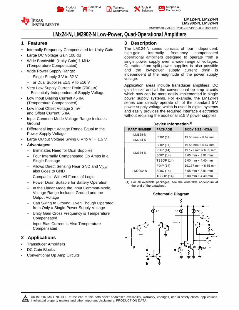
3 DescriptionThe LM124-N series consists of four independent,high-gain, internally frequency compensatedoperational amplifiers designed to operate from asingle power supply over a wide range of voltages.Operation from split-power supplies is also possibleand the low-power supply current drain isindependent of the magnitude of the power supplyvoltage.
Application areas include transducer amplifiers, DCgain blocks and all the conventional op amp circuitswhich now can be more easily implemented in singlepower supply systems. For example, the LM124-Nseries can directly operate off of the standard 5-Vpower supply voltage which is used in digital systemsand easily provides the required interface electronicswithout requiring the additional ±15 V power supplies.
Device Information(1)
PART NUMBER PACKAGE BODY SIZE (NOM)LM124-N
CDIP (14) 19.56 mm × 6.67 mmLM224-N
LM324-N
CDIP (14) 19.56 mm × 6.67 mmPDIP (14) 19.177 mm × 6.35 mmSOIC (14) 8.65 mm × 3.91 mmTSSOP (14) 5.00 mm × 4.40 mm
LM2902-NPDIP (14) 19.177 mm × 6.35 mmSOIC (14) 8.65 mm × 3.91 mmTSSOP (14) 5.00 mm × 4.40 mm
(1) For all available packages, see the orderable addendum atthe end of the datasheet.
Schematic Diagram

2
LM124-N, LM224-NLM2902-N, LM324-NSNOSC16D –MARCH 2000–REVISED JANUARY 2015 www.ti.com
Product Folder Links: LM124-N LM224-N LM2902-N LM324-N
Submit Documentation Feedback Copyright © 2000–2015, Texas Instruments Incorporated
Table of Contents1 Features .................................................................. 12 Applications ........................................................... 13 Description ............................................................. 14 Revision History..................................................... 25 Pin Configuration and Functions ......................... 36 Specifications......................................................... 4
6.1 Absolute Maximum Ratings ...................................... 46.2 ESD Ratings.............................................................. 46.3 Recommended Operating Conditions....................... 46.4 Thermal Information .................................................. 56.5 Electrical Characteristics: LM124A/224A/324A ........ 56.6 Electrical Characteristics: LM124-N/224-N/324-
N/2902-N ................................................................... 66.7 Typical Characteristics .............................................. 8
7 Detailed Description ............................................ 117.1 Overview ................................................................. 117.2 Functional Block Diagram ....................................... 11
7.3 Feature Description................................................. 117.4 Device Functional Modes........................................ 11
8 Application and Implementation ........................ 138.1 Application Information............................................ 138.2 Typical Applications ............................................... 13
9 Power Supply Recommendations ...................... 2310 Layout................................................................... 23
10.1 Layout Guidelines ................................................. 2310.2 Layout Example .................................................... 23
11 Device and Documentation Support ................. 2411.1 Related Links ........................................................ 2411.2 Trademarks ........................................................... 2411.3 Electrostatic Discharge Caution............................ 2411.4 Glossary ................................................................ 24
12 Mechanical, Packaging, and OrderableInformation ........................................................... 24
4 Revision History
Changes from Revision C (November 2012) to Revision D Page
• Added Pin Configuration and Functions section, ESD Ratings table, Feature Description section, Device FunctionalModes, Application and Implementation section, Power Supply Recommendations section, Layout section, Deviceand Documentation Support section, and Mechanical, Packaging, and Orderable Information section ............................... 1
3
LM124-N, LM224-NLM2902-N, LM324-N
www.ti.com SNOSC16D –MARCH 2000–REVISED JANUARY 2015
Product Folder Links: LM124-N LM224-N LM2902-N LM324-N
Submit Documentation FeedbackCopyright © 2000–2015, Texas Instruments Incorporated
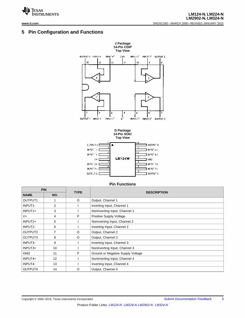
5 Pin Configuration and Functions
J Package14-Pin CDIP
Top View
D Package14-Pin SOIC
Top View
Pin FunctionsPIN
TYPE DESCRIPTIONNAME NO.OUTPUT1 1 O Output, Channel 1INPUT1- 2 I Inverting Input, Channel 1INPUT1+ 3 I Noninverting Input, Channel 1V+ 4 P Positive Supply VoltageINPUT2+ 5 I Nonnverting Input, Channel 2INPUT2- 6 I Inverting Input, Channel 2OUTPUT2 7 O Output, Channel 2OUTPUT3 8 O Output, Channel 3INPUT3- 9 I Inverting Input, Channel 3INPUT3+ 10 I Noninverting Input, Channel 3GND 11 P Ground or Negative Supply VoltageINPUT4+ 12 I Noninverting Input, Channel 4INPUT4- 13 I Inverting Input, Channel 4OUTPUT4 14 O Output, Channel 4

4
LM124-N, LM224-NLM2902-N, LM324-NSNOSC16D –MARCH 2000–REVISED JANUARY 2015 www.ti.com
Product Folder Links: LM124-N LM224-N LM2902-N LM324-N
Submit Documentation Feedback Copyright © 2000–2015, Texas Instruments Incorporated
(1) Refer to RETS124AX for LM124A military specifications and refer to RETS124X for LM124-N military specifications.(2) If Military/Aerospace specified devices are required, please contact the Texas Instruments Sales Office/ Distributors for availability and
specifications.(3) This input current will only exist when the voltage at any of the input leads is driven negative. It is due to the collector-base junction of
the input PNP transistors becoming forward biased and thereby acting as input diode clamps. In addition to this diode action, there isalso lateral NPN parasitic transistor action on the IC chip. This transistor action can cause the output voltages of the op amps to go tothe V+voltage level (or to ground for a large overdrive) for the time duration that an input is driven negative. This is not destructive andnormal output states will re-establish when the input voltage, which was negative, again returns to a value greater than −0.3 V (at 25°C).
(4) For operating at high temperatures, the LM324-N/LM324A/LM2902-N must be derated based on a 125°C maximum junctiontemperature and a thermal resistance of 88°C/W which applies for the device soldered in a printed circuit board, operating in a still airambient. The LM224-N/LM224A and LM124-N/LM124A can be derated based on a 150°C maximum junction temperature. Thedissipation is the total of all four amplifiers—use external resistors, where possible, to allow the amplifier to saturate of to reduce thepower which is dissipated in the integrated circuit.
(5) Short circuits from the output to V+ can cause excessive heating and eventual destruction. When considering short circuits to ground,the maximum output current is approximately 40 mA independent of the magnitude of V+. At values of supply voltage in excess of 15 V,continuous short-circuits can exceed the power dissipation ratings and cause eventual destruction. Destructive dissipation can resultfrom simultaneous shorts on all amplifiers.
6 Specifications
6.1 Absolute Maximum RatingsSee (1) (2).
LM124-N/LM224-N/LM324-NLM124A/LM224A/LM324A LM2902-N
MIN MAX MIN MAX UNITSupply Voltage, V+ 32 26 VDifferential Input Voltage 32 26 VInput Voltage −0.3 32 −0.3 26 VInput Current (VIN < −0.3 V) (3) 50 50 mAPowerDissipation (4)
PDIP 1130 1130 mWCDIP 1260 1260 mWSOIC Package 800 800 mW
Output Short-Circuit to GND(One Amplifier) (5) V+ ≤ 15 V and TA = 25°C Continuous Continuous
Lead Temperature (Soldering, 10 seconds) 260 260 °C
SolderingInformation
Dual-In-LinePackage
Soldering (10 seconds) 260 260 °C
SmallOutlinePackage
Vapor Phase (60 seconds) 215 215 °CInfrared (15 seconds) 220 220 °C
Storage temperature, Tstg –65 150 –65 150 °C
(1) JEDEC document JEP155 states that 500-V HBM allows safe manufacturing with a standard ESD control process.
6.2 ESD RatingsVALUE UNIT
V(ESD) Electrostatic discharge Human-body model (HBM), per ANSI/ESDA/JEDEC JS-001 (1) ±250 V
6.3 Recommended Operating Conditionsover operating free-air temperature range (unless otherwise noted)
MIN MAX UNITSupply Voltage (V+ - V-): LM124-N/LM124A/LM224-N/LM224A/LM324-N/LM324A 3 32 VSupply Voltage (V+ - V-): LM2902-N 3 26 VOperating Input Voltage on Input pins 0 V+ VOperating junction temperature, TJ: LM124-N/LM124A -55 125 °COperating junction temperature, TJ: L2902-N -40 85 °COperating junction temperature, TJ: LM224-N/LM224A -25 85 °COperating junction temperature, TJ: LM324-N/LM324A 0 70 °C

5
LM124-N, LM224-NLM2902-N, LM324-N
www.ti.com SNOSC16D –MARCH 2000–REVISED JANUARY 2015
Product Folder Links: LM124-N LM224-N LM2902-N LM324-N
Submit Documentation FeedbackCopyright © 2000–2015, Texas Instruments Incorporated
(1) For more information about traditional and new thermal metrics, see the IC Package Thermal Metrics application report, SPRA953.
6.4 Thermal Information
THERMAL METRIC (1)
LM124-N /LM224-N
LM324-N /LM2902-N
UNITJ/CDIP D/SOIC14 PINS 14 PINS
RθJA Junction-to-ambient thermal resistance 88 88 °C/W
(1) These specifications are limited to −55°C ≤ TA ≤ +125°C for the LM124-N/LM124A. With the LM224-N/LM224A, all temperaturespecifications are limited to −25°C ≤ TA ≤ +85°C, the LM324-N/LM324A temperature specifications are limited to 0°C ≤ TA ≤ +70°C, andthe LM2902-N specifications are limited to −40°C ≤ TA ≤ +85°C.
(2) VO ≃ 1.4V, RS = 0 Ω with V+ from 5 V to 30 V; and over the full input common-mode range (0 V to V+ − 1.5 V) for LM2902-N, V+ from 5V to 26 V.
(3) The direction of the input current is out of the IC due to the PNP input stage. This current is essentially constant, independent of thestate of the output so no loading change exists on the input lines.
(4) The input common-mode voltage of either input signal voltage should not be allowed to go negative by more than 0.3 V (at 25°C). Theupper end of the common-mode voltage range is V+ − 1.5 V (at 25°C), but either or both inputs can go to 32 V without damage (26 V forLM2902-N), independent of the magnitude of V+.
(5) Due to proximity of external components, insure that coupling is not originating via stray capacitance between these external parts. Thistypically can be detected as this type of capacitance increases at higher frequencies.
(6) Short circuits from the output to V+ can cause excessive heating and eventual destruction. When considering short circuits to ground,the maximum output current is approximately 40 mA independent of the magnitude of V+. At values of supply voltage in excess of 15 V,continuous short-circuits can exceed the power dissipation ratings and cause eventual destruction. Destructive dissipation can resultfrom simultaneous shorts on all amplifiers.
6.5 Electrical Characteristics: LM124A/224A/324AV+ = 5.0 V, (1), unless otherwise stated
PARAMETER TEST CONDITIONSLM124A LM224A LM324A
UNITMIN TYP MAX MIN TYP MAX MIN TYP MAX
Input Offset Voltage TA = 25°C (2) 1 2 1 3 2 3 mV
Input Bias Current (3) IIN(+) or IIN(−), VCM = 0 V,TA = 25°C 20 50 40 80 45 100 nA
Input Offset Current IIN(+) or IIN(−), VCM = 0 V,TA = 25°C 2 10 2 15 5 30 nA
Input Common-ModeVoltage Range (4)
V+ = 30 V, (LM2902-N,V+ = 26 V), TA = 25°C
0 V+−1.5 0 V+−1.5 0 V+−1.5 V
Supply Current
Over Full Temperature Range,RL = ∞ On All Op AmpsV+ = 30 V (LM2902-N V+ = 26 V)
1.5 3 1.5 3 1.5 3mA
V+ = 5 V 0.7 1.2 0.7 1.2 0.7 1.2
Large SignalVoltage Gain
V+ = 15 V, RL≥ 2 kΩ,(VO = 1 V to 11 V), TA = 25°C
50 100 50 100 25 100 V/mV
Common-ModeRejection Ratio
DC, VCM = 0 V to V+ − 1.5 V,TA = 25°C
70 85 70 85 65 85 dB
Power SupplyRejection Ratio
V+ = 5 V to 30 V, (LM2902-N,V+ = 5V to 26 V),TA = 25°C
65 100 65 100 65 100 dB
Amplifier-to-AmplifierCoupling (5)
f = 1 kHz to 20 kHz, TA = 25°C,(Input Referred) −120 −120 −120 dB
OutputCurrent
Source VIN+ = 1 V, VIN
− = 0 V,V+ = 15 V, VO = 2 V, TA = 25°C
20 40 20 40 20 40 mA
Sink
VIN− = 1 V, VIN
+ = 0 V,V+ = 15 V, VO = 2 V, TA = 25°C
10 20 10 20 10 20
μAVIN
− = 1 V, VIN+ = 0 V,
V+ = 15 V, VO = 200 mV, TA = 25°C12 50 12 50 12 50
Short Circuit to Ground V+ = 15 V,TA = 25°C (6) 40 60 40 60 40 60 mA
Input Offset Voltage See (2) 4 4 5 mV
VOS Drift RS = 0 Ω 7 20 7 20 7 30 μV/°C
Input Offset Current IIN(+) − IIN(−), VCM = 0 V 30 30 75 nA

6
LM124-N, LM224-NLM2902-N, LM324-NSNOSC16D –MARCH 2000–REVISED JANUARY 2015 www.ti.com
Product Folder Links: LM124-N LM224-N LM2902-N LM324-N
Submit Documentation Feedback Copyright © 2000–2015, Texas Instruments Incorporated
Electrical Characteristics: LM124A/224A/324A (continued)V+ = 5.0 V, (1), unless otherwise stated
PARAMETER TEST CONDITIONSLM124A LM224A LM324A
UNITMIN TYP MAX MIN TYP MAX MIN TYP MAX
IOS Drift RS = 0 Ω 10 200 10 200 10 300 pA/°C
Input Bias Current IIN(+) or IIN(−) 40 100 40 100 40 200 nA
Input Common-ModeVoltage Range (4)
V+ = 30 V,(LM2902-N, V+ = 26 V)
0 V+−2 0 V+−2 0 V+−2 V
Large SignalVoltage Gain
V+ = 15 V (VOSwing = 1 V to 11 V),RL ≥ 2 kΩ 25 25 15 V/mV
OutputVoltageSwing
VOH
V+ = 30 V(LM2902-N,V+ = 26 V)
RL = 2 kΩ 26 26 26VRL = 10 kΩ 27 28 27 28 27 28
VOL V+ = 5 V, RL = 10 kΩ 5 20 5 20 5 20 mV
OutputCurrent
Source
VO = 2 V
VIN+ = +1V,
VIN− = 0V,
V+ = 15V10 20 10 20 10 20
mA
SinkVIN
− = +1V,VIN
+ = 0V,V+ = 15V
10 15 5 8 5 8
(1) These specifications are limited to −55°C ≤ TA ≤ +125°C for the LM124-N/LM124A. With the LM224-N/LM224A, all temperaturespecifications are limited to −25°C ≤ TA ≤ +85°C, the LM324-N/LM324A temperature specifications are limited to 0°C ≤ TA ≤ +70°C, andthe LM2902-N specifications are limited to −40°C ≤ TA ≤ +85°C.
(2) VO ≃ 1.4V, RS = 0 Ω with V+ from 5 V to 30 V; and over the full input common-mode range (0 V to V+ − 1.5 V) for LM2902-N, V+ from 5V to 26 V.
(3) The direction of the input current is out of the IC due to the PNP input stage. This current is essentially constant, independent of thestate of the output so no loading change exists on the input lines.
(4) The input common-mode voltage of either input signal voltage should not be allowed to go negative by more than 0.3 V (at 25°C). Theupper end of the common-mode voltage range is V+ − 1.5 V (at 25°C), but either or both inputs can go to 32 V without damage (26 V forLM2902-N), independent of the magnitude of V+.
(5) Due to proximity of external components, insure that coupling is not originating via stray capacitance between these external parts. Thistypically can be detected as this type of capacitance increases at higher frequencies.
6.6 Electrical Characteristics: LM124-N/224-N/324-N/2902-NV+ = +5.0V, (1), unless otherwise stated
PARAMETER TEST CONDITIONSLM124-N / LM224-N LM324-N LM2902-N
UNITMIN TYP MAX MIN TYP MAX MIN TYP MAX
Input Offset Voltage TA = 25°C (2) 2 5 2 7 2 7 mV
Input Bias Current (3) IIN(+) or IIN(−), VCM = 0 V, TA = 25°C 45 150 45 250 45 250 nA
Input Offset Current IIN(+) or IIN(−), VCM = 0 V, TA = 25°C 3 30 5 50 5 50 nA
Input Common-Mode VoltageRange (4)
V+ = 30 V, (LM2902-N, V+ = 26V),TA = 25°C
0 V+−1.5 0 V+−1.
5 0 V+−1.5 V
Supply Current
Over Full Temperature RangeRL = ∞ On All Op Amps,V+ = 30 V (LM2902-N V+ = 26 V)
1.5 3 1.5 3 1.5 3mA
V+ = 5 V 0.7 1.2 0.7 1.2 0.7 1.2
Large Signal Voltage Gain V+ = 15V, RL≥ 2 kΩ,(VO = 1 V to 11 V), TA = 25°C
50 100 25 100 25 100 V/mV
Common-Mode RejectionRatio DC, VCM = 0 V to V+ − 1.5 V, TA = 25°C 70 85 65 85 50 70 dB
Power Supply Rejection Ratio V+ = 5 V to 30 V (LM2902-N,V+ = 5 V to 26 V), TA = 25°C
65 100 65 100 50 100 dB
Amplifier-to-AmplifierCoupling (5)
f = 1 kHz to 20 kHz, TA = 25°C(Input Referred) −120 −120 −120 dB

7
LM124-N, LM224-NLM2902-N, LM324-N
www.ti.com SNOSC16D –MARCH 2000–REVISED JANUARY 2015
Product Folder Links: LM124-N LM224-N LM2902-N LM324-N
Submit Documentation FeedbackCopyright © 2000–2015, Texas Instruments Incorporated
Electrical Characteristics: LM124-N/224-N/324-N/2902-N (continued)V+ = +5.0V, (1), unless otherwise stated
PARAMETER TEST CONDITIONSLM124-N / LM224-N LM324-N LM2902-N
UNITMIN TYP MAX MIN TYP MAX MIN TYP MAX
(6) Short circuits from the output to V+ can cause excessive heating and eventual destruction. When considering short circuits to ground,the maximum output current is approximately 40 mA independent of the magnitude of V+. At values of supply voltage in excess of 15 V,continuous short-circuits can exceed the power dissipation ratings and cause eventual destruction. Destructive dissipation can resultfrom simultaneous shorts on all amplifiers.
OutputCurrent
Source VIN+ = 1 V, VIN
− = 0 V,V+ = 15 V, VO = 2 V, TA = 25°C
20 40 20 40 20 40 mA
Sink
VIN− = 1 V, VIN
+ = 0 V,V+ = 15 V, VO = 2 V, TA = 25°C
10 20 10 20 10 20 mA
VIN− = 1 V, VIN
+ = 0 V,V+ = 15 V, VO = 200 mV, TA = 25°C
12 50 12 50 12 50 µA
Short Circuit to Ground V+ = 15 V, TA = 25°C (6) 40 60 40 60 40 60 mA
Input Offset Voltage See (2) 7 9 10 mV
VOS Drift RS = 0 Ω 7 7 7 µV/°C
Input Offset Current IIN(+) − IIN(−), VCM = 0 V 100 150 45 200 nA
IOS Drift RS = 0 Ω 10 10 10 pA/°C
Input Bias Current IIN(+) or IIN(−) 40 300 40 500 40 500 nA
Input Common-Mode VoltageRange (4) V+ = 30 V, (LM2902-N, V+ = 26 V) 0 V+−2 0 V+−2 0 V+−2 V
Large Signal Voltage Gain V+ = 15 V (VOSwing = 1V to 11V),RL ≥ 2 kΩ
25 15 15 V/mV
OutputVoltageSwing
VOHV+ = 30 V (LM2902-N,V+ = 26 V)
RL = 2 kΩ 26 26 22V
RL = 10 kΩ 27 28 27 28 23 24
VOL V+ = 5 V, RL = 10 kΩ 5 20 5 20 5 100 mV
OutputCurrent
Source VO = 2 VVIN
+ = 1 V,VIN
− = 0 V,V+ = 15 V
10 20 10 20 10 20 mA
SinkVIN
− = 1 V,VIN
+ = 0 V,V+ = 15 V
5 8 5 8 5 8 mA

8
LM124-N, LM224-NLM2902-N, LM324-NSNOSC16D –MARCH 2000–REVISED JANUARY 2015 www.ti.com
Product Folder Links: LM124-N LM224-N LM2902-N LM324-N
Submit Documentation Feedback Copyright © 2000–2015, Texas Instruments Incorporated
6.7 Typical Characteristics
Figure 1. Input Voltage Range Figure 2. Input Current
Figure 3. Supply Current Figure 4. Voltage Gain
Figure 5. Open-Loop Frequency Response Figure 6. Common Mode Rejection Ratio

9
LM124-N, LM224-NLM2902-N, LM324-N
www.ti.com SNOSC16D –MARCH 2000–REVISED JANUARY 2015
Product Folder Links: LM124-N LM224-N LM2902-N LM324-N
Submit Documentation FeedbackCopyright © 2000–2015, Texas Instruments Incorporated
Typical Characteristics (continued)
Figure 7. Voltage Follower Pulse Response Figure 8. Voltage Follower Pulse Response (Small Signal)
Figure 9. Large Signal Frequency Response Figure 10. Output Characteristics Current Sourcing
Figure 11. Output Characteristics Current Sinking Figure 12. Current Limiting

10
LM124-N, LM224-NLM2902-N, LM324-NSNOSC16D –MARCH 2000–REVISED JANUARY 2015 www.ti.com
Product Folder Links: LM124-N LM224-N LM2902-N LM324-N
Submit Documentation Feedback Copyright © 2000–2015, Texas Instruments Incorporated
Typical Characteristics (continued)
Figure 13. Input Current (LM2902-N Only) Figure 14. Voltage Gain (LM2902-N Only)

11
LM124-N, LM224-NLM2902-N, LM324-N
www.ti.com SNOSC16D –MARCH 2000–REVISED JANUARY 2015
Product Folder Links: LM124-N LM224-N LM2902-N LM324-N
Submit Documentation FeedbackCopyright © 2000–2015, Texas Instruments Incorporated
7 Detailed Description
7.1 OverviewThe LM124-N series are op amps which operate with only a single power supply voltage, have true-differentialinputs, and remain in the linear mode with an input common-mode voltage of 0 VDC. These amplifiers operateover a wide range of power supply voltage with little change in performance characteristics. At 25°C amplifieroperation is possible down to a minimum supply voltage of 2.3 VDC.
7.2 Functional Block Diagram
7.3 Feature DescriptionThe LM124 provides a compelling balance of performance versus current consumption. The 700 μA of supplycurrent draw over the wide operating conditions with a 1-MHz gain-bandwidth and temperature compensatedbias currents makes the LM124 an effective solution for large variety of applications. The input offset voltage of 2mV and offset current of 5 nA, along with the 45n-A bias current across a wide supply voltage means a singledesign can be used in a large number of different implementations.
7.4 Device Functional ModesLarge differential input voltages can be easily accommodated and, as input differential voltage protection diodesare not needed, no large input currents result from large differential input voltages. The differential input voltagemay be larger than V+ without damaging the device. Protection should be provided to prevent the input voltagesfrom going negative more than −0.3 VDC (at 25°C). An input clamp diode with a resistor to the IC input terminalcan be used.
To reduce the power supply drain, the amplifiers have a class A output stage for small signal levels whichconverts to class B in a large signal mode. This allows the amplifiers to both source and sink large outputcurrents. Therefore both NPN and PNP external current boost transistors can be used to extend the powercapability of the basic amplifiers. The output voltage needs to raise approximately 1 diode drop above ground tobias the on-chip vertical PNP transistor for output current sinking applications.
For ac applications, where the load is capacitively coupled to the output of the amplifier, a resistor should beused, from the output of the amplifier to ground to increase the class A bias current and prevent crossoverdistortion.
Where the load is directly coupled, as in dc applications, there is no crossover distortion.
Capacitive loads which are applied directly to the output of the amplifier reduce the loop stability margin. Valuesof 50 pF can be accommodated using the worst-case non-inverting unity gain connection. Large closed loopgains or resistive isolation should be used if larger load capacitance must be driven by the amplifier.
12
LM124-N, LM224-NLM2902-N, LM324-NSNOSC16D –MARCH 2000–REVISED JANUARY 2015 www.ti.com
Product Folder Links: LM124-N LM224-N LM2902-N LM324-N
Submit Documentation Feedback Copyright © 2000–2015, Texas Instruments Incorporated
Device Functional Modes (continued)The bias network of the LM124-N establishes a drain current which is independent of the magnitude of the powersupply voltage over the range of from 3 VDC to 30 VDC.
Output short circuits either to ground or to the positive power supply should be of short time duration. Units canbe destroyed, not as a result of the short circuit current causing metal fusing, but rather due to the large increasein IC chip dissipation which will cause eventual failure due to excessive junction temperatures. Putting directshort-circuits on more than one amplifier at a time will increase the total IC power dissipation to destructivelevels, if not properly protected with external dissipation limiting resistors in series with the output leads of theamplifiers. The larger value of output source current which is available at 25°C provides a larger output currentcapability at elevated temperatures (see Typical Characteristics) than a standard IC op amp.
13
LM124-N, LM224-NLM2902-N, LM324-N
www.ti.com SNOSC16D –MARCH 2000–REVISED JANUARY 2015
Product Folder Links: LM124-N LM224-N LM2902-N LM324-N
Submit Documentation FeedbackCopyright © 2000–2015, Texas Instruments Incorporated
8 Application and Implementation
NOTEInformation in the following applications sections is not part of the TI componentspecification, and TI does not warrant its accuracy or completeness. TI’s customers areresponsible for determining suitability of components for their purposes. Customers shouldvalidate and test their design implementation to confirm system functionality.
8.1 Application InformationThe LM124 series of amplifiers is specified for operation from 3 V to 32 V (±1.5 V to ±16 V). Many of thespecifications apply from –40°C to 125°C. Parameters that can exhibit significant variance with regards tooperating voltage or temperature are presented in Typical Characteristics.
8.2 Typical ApplicationsFigure 15 emphasizes operation on only a single power supply voltage. If complementary power supplies areavailable, all of the standard op amp circuits can be used. In general, introducing a pseudo-ground (a biasvoltage reference of V+/2) will allow operation above and below this value in single power supply systems. Manyapplication circuits are shown which take advantage of the wide input common-mode voltage range whichincludes ground. In most cases, input biasing is not required and input voltages which range to ground can easilybe accommodated.
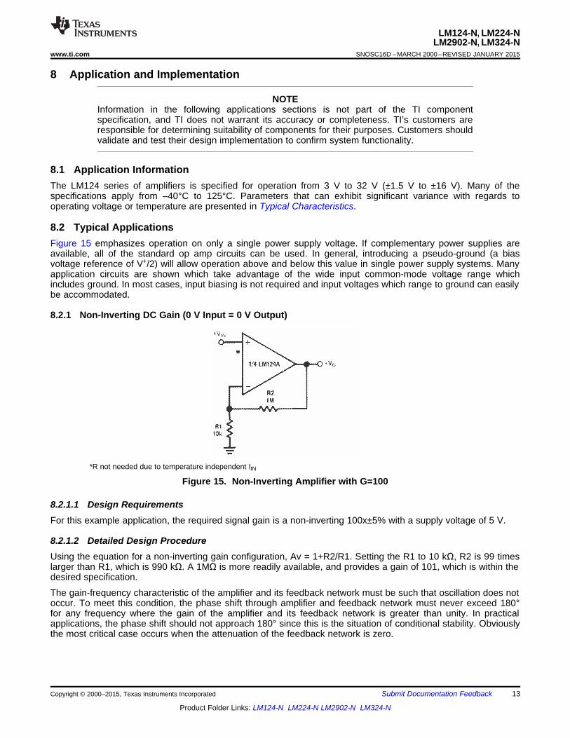
8.2.1 Non-Inverting DC Gain (0 V Input = 0 V Output)
*R not needed due to temperature independent IIN
Figure 15. Non-Inverting Amplifier with G=100
8.2.1.1 Design RequirementsFor this example application, the required signal gain is a non-inverting 100x±5% with a supply voltage of 5 V.
8.2.1.2 Detailed Design ProcedureUsing the equation for a non-inverting gain configuration, Av = 1+R2/R1. Setting the R1 to 10 kΩ, R2 is 99 timeslarger than R1, which is 990 kΩ. A 1MΩ is more readily available, and provides a gain of 101, which is within thedesired specification.
The gain-frequency characteristic of the amplifier and its feedback network must be such that oscillation does notoccur. To meet this condition, the phase shift through amplifier and feedback network must never exceed 180°for any frequency where the gain of the amplifier and its feedback network is greater than unity. In practicalapplications, the phase shift should not approach 180° since this is the situation of conditional stability. Obviouslythe most critical case occurs when the attenuation of the feedback network is zero.

14
LM124-N, LM224-NLM2902-N, LM324-NSNOSC16D –MARCH 2000–REVISED JANUARY 2015 www.ti.com
Product Folder Links: LM124-N LM224-N LM2902-N LM324-N
Submit Documentation Feedback Copyright © 2000–2015, Texas Instruments Incorporated
Typical Applications (continued)8.2.1.3 Application Curve
Figure 16. Non-Inverting Amplified Response Curve

15
LM124-N, LM224-NLM2902-N, LM324-N
www.ti.com SNOSC16D –MARCH 2000–REVISED JANUARY 2015
Product Folder Links: LM124-N LM224-N LM2902-N LM324-N
Submit Documentation FeedbackCopyright © 2000–2015, Texas Instruments Incorporated
Typical Applications (continued)8.2.2 Other Application Circuits at V+ = 5.0 VDC
Where: V0 = V1 + V2 − V3 − V4
(V1 + V2) ≥ (V3 + V4) to keep VO > 0 VDC
Where: V0 = 0 VDC for VIN = 0 VDC
AV = 10
Figure 17. DC Summing Amplifier(VIN'S ≥ 0 VDC And VO ≥ VDC)
Figure 18. Power Amplifier
fo = 1 kHz Q = 50 AV = 100 (40 dB)
Figure 19. LED Driver Figure 20. “BI-QUAD” RC Active Bandpass Filter

16
LM124-N, LM224-NLM2902-N, LM324-NSNOSC16D –MARCH 2000–REVISED JANUARY 2015 www.ti.com
Product Folder Links: LM124-N LM224-N LM2902-N LM324-N
Submit Documentation Feedback Copyright © 2000–2015, Texas Instruments Incorporated
Typical Applications (continued)
Figure 21. Fixed Current Sources
*(Increase R1 for IL small)
Figure 22. Lamp Driver Figure 23. Current Monitor
Figure 24. Driving TTL Figure 25. Voltage Follower

17
LM124-N, LM224-NLM2902-N, LM324-N
www.ti.com SNOSC16D –MARCH 2000–REVISED JANUARY 2015
Product Folder Links: LM124-N LM224-N LM2902-N LM324-N
Submit Documentation FeedbackCopyright © 2000–2015, Texas Instruments Incorporated
Typical Applications (continued)
Figure 26. Pulse Generator Figure 27. Squarewave Oscillator
IO = 1 amp/volt VIN (Increase RE for Io small)
Figure 28. Pulse Generator Figure 29. High Compliance Current Sink

18
LM124-N, LM224-NLM2902-N, LM324-NSNOSC16D –MARCH 2000–REVISED JANUARY 2015 www.ti.com
Product Folder Links: LM124-N LM224-N LM2902-N LM324-N
Submit Documentation Feedback Copyright © 2000–2015, Texas Instruments Incorporated
Typical Applications (continued)
Figure 30. Low Drift Peak Detector Figure 31. Comparator With Hysteresis
VO = VR
*Wide control voltage range:0 VDC ≤ VC ≤ 2 (V+ −1.5 VDC)
Figure 32. Ground Referencing a Differential InputSignal
Figure 33. Voltage Controlled Oscillator Circuit

19
LM124-N, LM224-NLM2902-N, LM324-N
www.ti.com SNOSC16D –MARCH 2000–REVISED JANUARY 2015
Product Folder Links: LM124-N LM224-N LM2902-N LM324-N
Submit Documentation FeedbackCopyright © 2000–2015, Texas Instruments Incorporated
Typical Applications (continued)
Q = 1 AV = 2
Figure 34. Photo Voltaic-Cell Amplifier Figure 35. DC Coupled Low-Pass RC Active Filter
Figure 36. AC Coupled Inverting Amplifier
Figure 37. AC Coupled Non-Inverting Amplifier

20
LM124-N, LM224-NLM2902-N, LM324-NSNOSC16D –MARCH 2000–REVISED JANUARY 2015 www.ti.com
Product Folder Links: LM124-N LM224-N LM2902-N LM324-N
Submit Documentation Feedback Copyright © 2000–2015, Texas Instruments Incorporated
Typical Applications (continued)
Figure 38. High Input Z, DC Differential Amplifier
Figure 39. High Input Z Adjustable-Gain DC Instrumentation Amplifier

21
LM124-N, LM224-NLM2902-N, LM324-N
www.ti.com SNOSC16D –MARCH 2000–REVISED JANUARY 2015
Product Folder Links: LM124-N LM224-N LM2902-N LM324-N
Submit Documentation FeedbackCopyright © 2000–2015, Texas Instruments Incorporated
Typical Applications (continued)
Figure 40. Bridge Current Amplifier
Figure 41. Using Symmetrical Amplifiers to Reduce Input Current (General Concept)

22
LM124-N, LM224-NLM2902-N, LM324-NSNOSC16D –MARCH 2000–REVISED JANUARY 2015 www.ti.com
Product Folder Links: LM124-N LM224-N LM2902-N LM324-N
Submit Documentation Feedback Copyright © 2000–2015, Texas Instruments Incorporated
Typical Applications (continued)
fO = 1 kHz Q = 25
Figure 42. Bandpass Active Filter

1: VOUTA 14: VOUTD
13: IN-D
12: IN+D
11: GND
10: IN+C
9: IN-C
8: VOUTC
2: IN-A
3: IN+A
4: V+
5: IN+B
6: IN-B
7: VOUTB
2
GND
2
GND
2
GND
2
GND
2
VOUTA
2
VOUTB
2
VOUTC
2
VOUTD
2
IN+B
2
IN+A 2
IN+D
2
IN+C
1
GND
2
V+
1
IN-A
1
IN-A
1
IN-D
1
IN-D
1
IN-C
1
IN-C
1
IN-B
1
IN-B
1
VINA
1
VINB
1
VIND
1
VINC
GND GND
GNDGND
GND GND
V+
IN+A
IN+B
IN-B
IN-A
IN+C VINC
IN-C
IN+D
IN-D
VOUTB VOUTC
VOUTA VOUTD
VO
UTA
VO
UT
D
VIN
C
VIN
D
GN
DG
ND
GN
D
VIN
C
23
LM124-N, LM224-NLM2902-N, LM324-N
www.ti.com SNOSC16D –MARCH 2000–REVISED JANUARY 2015
Product Folder Links: LM124-N LM224-N LM2902-N LM324-N
Submit Documentation FeedbackCopyright © 2000–2015, Texas Instruments Incorporated
9 Power Supply RecommendationsThe pinouts of the package have been designed to simplify PC board layouts. Inverting inputs are adjacent tooutputs for all of the amplifiers and the outputs have also been placed at the corners of the package (pins 1, 7, 8,and 14).
Precautions should be taken to insure that the power supply for the integrated circuit never becomes reversed inpolarity or that the unit is not inadvertently installed backwards in a test socket as an unlimited current surgethrough the resulting forward diode within the IC could cause fusing of the internal conductors and result in adestroyed unit.
10 Layout
10.1 Layout GuidelinesThe V + pin should be bypassed to ground with a low-ESR capacitor. The optimum placement is closest to the V+ and ground pins.
Take care to minimize the loop area formed by the bypass capacitor connection between V + and ground.
The ground pin should be connected to the PCB ground plane at the pin of the device.
The feedback components should be placed as close to the device as possible minimizing strays.
10.2 Layout Example
Figure 43. Layout Example

24
LM124-N, LM224-NLM2902-N, LM324-NSNOSC16D –MARCH 2000–REVISED JANUARY 2015 www.ti.com
Product Folder Links: LM124-N LM224-N LM2902-N LM324-N
Submit Documentation Feedback Copyright © 2000–2015, Texas Instruments Incorporated
11 Device and Documentation Support
11.1 Related LinksThe table below lists quick access links. Categories include technical documents, support and communityresources, tools and software, and quick access to sample or buy.
Table 1. Related Links
PARTS PRODUCT FOLDER SAMPLE & BUY TECHNICALDOCUMENTS
TOOLS &SOFTWARE
SUPPORT &COMMUNITY
LM124-N Click here Click here Click here Click here Click hereLM224-N Click here Click here Click here Click here Click hereLM2902-N Click here Click here Click here Click here Click hereLM324-N Click here Click here Click here Click here Click here
11.2 TrademarksAll trademarks are the property of their respective owners.
11.3 Electrostatic Discharge CautionThese devices have limited built-in ESD protection. The leads should be shorted together or the device placed in conductive foamduring storage or handling to prevent electrostatic damage to the MOS gates.
11.4 GlossarySLYZ022 — TI Glossary.
This glossary lists and explains terms, acronyms, and definitions.
12 Mechanical, Packaging, and Orderable InformationThe following pages include mechanical, packaging, and orderable information. This information is the mostcurrent data available for the designated devices. This data is subject to change without notice and revision ofthis document. For browser-based versions of this data sheet, refer to the left-hand navigation.

PACKAGE OPTION ADDENDUM
www.ti.com 26-Sep-2017
Addendum-Page 1
PACKAGING INFORMATION
Orderable Device Status(1)
Package Type PackageDrawing
Pins PackageQty
Eco Plan(2)
Lead/Ball Finish(6)
MSL Peak Temp(3)
Op Temp (°C) Device Marking(4/5)
Samples
LM124AJ/PB ACTIVE CDIP J 14 25 TBD Call TI Call TI -55 to 125 LM124AJ
LM124J/PB ACTIVE CDIP J 14 25 TBD Call TI Call TI -55 to 125 LM124J
LM224J ACTIVE CDIP J 14 25 TBD Call TI Call TI -25 to 85 LM224J
LM2902M NRND SOIC D 14 55 TBD Call TI Call TI -40 to 85 LM2902M
LM2902M/NOPB ACTIVE SOIC D 14 55 Green (RoHS& no Sb/Br)
CU SN Level-1-260C-UNLIM -40 to 85 LM2902M
LM2902MT NRND TSSOP PW 14 94 TBD Call TI Call TI -40 to 85 LM2902MT
LM2902MT/NOPB ACTIVE TSSOP PW 14 94 Green (RoHS& no Sb/Br)
CU SN Level-1-260C-UNLIM -40 to 85 LM2902MT
LM2902MTX/NOPB ACTIVE TSSOP PW 14 2500 Green (RoHS& no Sb/Br)
CU SN Level-1-260C-UNLIM -40 to 85 LM2902MT
LM2902MX NRND SOIC D 14 2500 TBD Call TI Call TI -40 to 85 LM2902M
LM2902MX/NOPB ACTIVE SOIC D 14 2500 Green (RoHS& no Sb/Br)
CU SN Level-1-260C-UNLIM -40 to 85 LM2902M
LM2902N/NOPB ACTIVE PDIP NFF 14 25 Green (RoHS& no Sb/Br)
CU SN Level-1-NA-UNLIM -40 to 85 LM2902N
LM324AM NRND SOIC D 14 55 TBD Call TI Call TI 0 to 70 LM324AM
LM324AM/NOPB ACTIVE SOIC D 14 55 Green (RoHS& no Sb/Br)
CU SN Level-1-260C-UNLIM 0 to 70 LM324AM
LM324AMX NRND SOIC D 14 2500 TBD Call TI Call TI 0 to 70 LM324AM
LM324AMX/NOPB ACTIVE SOIC D 14 2500 Green (RoHS& no Sb/Br)
CU SN Level-1-260C-UNLIM 0 to 70 LM324AM
LM324AN/NOPB ACTIVE PDIP NFF 14 25 Green (RoHS& no Sb/Br)
CU SN Level-1-NA-UNLIM 0 to 70 LM324AN
LM324M NRND SOIC D 14 55 TBD Call TI Call TI 0 to 70 LM324M
LM324M/NOPB ACTIVE SOIC D 14 55 Green (RoHS& no Sb/Br)
CU SN Level-1-260C-UNLIM 0 to 70 LM324M
LM324MT/NOPB ACTIVE TSSOP PW 14 94 Green (RoHS& no Sb/Br)
CU SN Level-1-260C-UNLIM 0 to 70 LM324MT
LM324MTX/NOPB ACTIVE TSSOP PW 14 2500 Green (RoHS& no Sb/Br)
CU SN Level-1-260C-UNLIM 0 to 70 LM324MT

PACKAGE OPTION ADDENDUM
www.ti.com 26-Sep-2017
Addendum-Page 2
Orderable Device Status(1)
Package Type PackageDrawing
Pins PackageQty
Eco Plan(2)
Lead/Ball Finish(6)
MSL Peak Temp(3)
Op Temp (°C) Device Marking(4/5)
Samples
LM324MX NRND SOIC D 14 2500 TBD Call TI Call TI 0 to 70 LM324M
LM324MX/NOPB ACTIVE SOIC D 14 2500 Green (RoHS& no Sb/Br)
CU SN Level-1-260C-UNLIM 0 to 70 LM324M
LM324N/NOPB ACTIVE PDIP NFF 14 25 Green (RoHS& no Sb/Br)
CU SN Level-1-NA-UNLIM 0 to 70 LM324N
(1) The marketing status values are defined as follows:ACTIVE: Product device recommended for new designs.LIFEBUY: TI has announced that the device will be discontinued, and a lifetime-buy period is in effect.NRND: Not recommended for new designs. Device is in production to support existing customers, but TI does not recommend using this part in a new design.PREVIEW: Device has been announced but is not in production. Samples may or may not be available.OBSOLETE: TI has discontinued the production of the device.
(2) RoHS: TI defines "RoHS" to mean semiconductor products that are compliant with the current EU RoHS requirements for all 10 RoHS substances, including the requirement that RoHS substancedo not exceed 0.1% by weight in homogeneous materials. Where designed to be soldered at high temperatures, "RoHS" products are suitable for use in specified lead-free processes. TI mayreference these types of products as "Pb-Free".RoHS Exempt: TI defines "RoHS Exempt" to mean products that contain lead but are compliant with EU RoHS pursuant to a specific EU RoHS exemption.Green: TI defines "Green" to mean the content of Chlorine (Cl) and Bromine (Br) based flame retardants meet JS709B low halogen requirements of <=1000ppm threshold. Antimony trioxide basedflame retardants must also meet the <=1000ppm threshold requirement.
(3) MSL, Peak Temp. - The Moisture Sensitivity Level rating according to the JEDEC industry standard classifications, and peak solder temperature.
(4) There may be additional marking, which relates to the logo, the lot trace code information, or the environmental category on the device.
(5) Multiple Device Markings will be inside parentheses. Only one Device Marking contained in parentheses and separated by a "~" will appear on a device. If a line is indented then it is a continuationof the previous line and the two combined represent the entire Device Marking for that device.
(6) Lead/Ball Finish - Orderable Devices may have multiple material finish options. Finish options are separated by a vertical ruled line. Lead/Ball Finish values may wrap to two lines if the finishvalue exceeds the maximum column width.
Important Information and Disclaimer:The information provided on this page represents TI's knowledge and belief as of the date that it is provided. TI bases its knowledge and belief on informationprovided by third parties, and makes no representation or warranty as to the accuracy of such information. Efforts are underway to better integrate information from third parties. TI has taken andcontinues to take reasonable steps to provide representative and accurate information but may not have conducted destructive testing or chemical analysis on incoming materials and chemicals.TI and TI suppliers consider certain information to be proprietary, and thus CAS numbers and other limited information may not be available for release.
In no event shall TI's liability arising out of such information exceed the total purchase price of the TI part(s) at issue in this document sold by TI to Customer on an annual basis.

PACKAGE OPTION ADDENDUM
www.ti.com 26-Sep-2017
Addendum-Page 3
OTHER QUALIFIED VERSIONS OF LM124-N, LM2902-N :
• Automotive: LM2902-Q1
• Enhanced Product: LM2902-EP
• Space: LM124-SP
NOTE: Qualified Version Definitions:
• Automotive - Q100 devices qualified for high-reliability automotive applications targeting zero defects
• Enhanced Product - Supports Defense, Aerospace and Medical Applications
• Space - Radiation tolerant, ceramic packaging and qualified for use in Space-based application

TAPE AND REEL INFORMATION
*All dimensions are nominal
Device PackageType
PackageDrawing
Pins SPQ ReelDiameter
(mm)
ReelWidth
W1 (mm)
A0(mm)
B0(mm)
K0(mm)
P1(mm)
W(mm)
Pin1Quadrant
LM2902MTX/NOPB TSSOP PW 14 2500 330.0 12.4 6.95 5.6 1.6 8.0 12.0 Q1
LM2902MX SOIC D 14 2500 330.0 16.4 6.5 9.35 2.3 8.0 16.0 Q1
LM2902MX/NOPB SOIC D 14 2500 330.0 16.4 6.5 9.35 2.3 8.0 16.0 Q1
LM324AMX SOIC D 14 2500 330.0 16.4 6.5 9.35 2.3 8.0 16.0 Q1
LM324AMX/NOPB SOIC D 14 2500 330.0 16.4 6.5 9.35 2.3 8.0 16.0 Q1
LM324MTX/NOPB TSSOP PW 14 2500 330.0 12.4 6.95 5.6 1.6 8.0 12.0 Q1
LM324MX SOIC D 14 2500 330.0 16.4 6.5 9.35 2.3 8.0 16.0 Q1
LM324MX/NOPB SOIC D 14 2500 330.0 16.4 6.5 9.35 2.3 8.0 16.0 Q1
PACKAGE MATERIALS INFORMATION
www.ti.com 24-Aug-2017
Pack Materials-Page 1

*All dimensions are nominal
Device Package Type Package Drawing Pins SPQ Length (mm) Width (mm) Height (mm)
LM2902MTX/NOPB TSSOP PW 14 2500 367.0 367.0 35.0
LM2902MX SOIC D 14 2500 367.0 367.0 35.0
LM2902MX/NOPB SOIC D 14 2500 367.0 367.0 35.0
LM324AMX SOIC D 14 2500 367.0 367.0 35.0
LM324AMX/NOPB SOIC D 14 2500 367.0 367.0 35.0
LM324MTX/NOPB TSSOP PW 14 2500 367.0 367.0 35.0
LM324MX SOIC D 14 2500 367.0 367.0 35.0
LM324MX/NOPB SOIC D 14 2500 367.0 367.0 35.0
PACKAGE MATERIALS INFORMATION
www.ti.com 24-Aug-2017
Pack Materials-Page 2


www.ti.com
PACKAGE OUTLINE
C
14X .008-.014 [0.2-0.36]TYP
-150
AT GAGE PLANE
-.314.308-7.977.83[ ]
14X -.026.014-0.660.36[ ]14X -.065.045
-1.651.15[ ]
.2 MAX TYP[5.08]
.13 MIN TYP[3.3]
TYP-.060.015-1.520.38[ ]
4X .005 MIN[0.13]
12X .100[2.54]
.015 GAGE PLANE[0.38]
A
-.785.754-19.9419.15[ ]
B -.283.245-7.196.22[ ]
CDIP - 5.08 mm max heightJ0014ACERAMIC DUAL IN LINE PACKAGE
4214771/A 05/2017
NOTES: 1. All controlling linear dimensions are in inches. Dimensions in brackets are in millimeters. Any dimension in brackets or parenthesis are for reference only. Dimensioning and tolerancing per ASME Y14.5M.2. This drawing is subject to change without notice. 3. This package is hermitically sealed with a ceramic lid using glass frit.4. Index point is provided on cap for terminal identification only and on press ceramic glass frit seal only.5. Falls within MIL-STD-1835 and GDIP1-T14.
7 8
141
PIN 1 ID(OPTIONAL)
SCALE 0.900
SEATING PLANE
.010 [0.25] C A B
www.ti.com
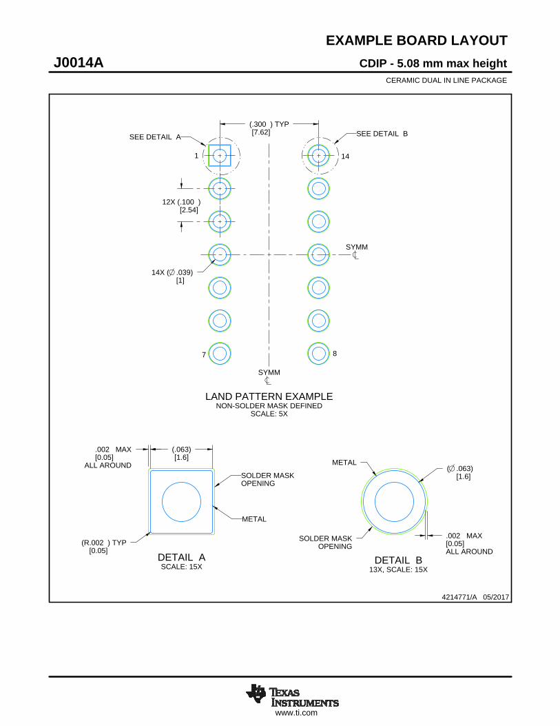
EXAMPLE BOARD LAYOUT
ALL AROUND[0.05]
MAX.002
.002 MAX[0.05]ALL AROUND
SOLDER MASKOPENING
METAL
(.063)[1.6]
(R.002 ) TYP[0.05]
14X ( .039)[1]
( .063)[1.6]
12X (.100 )[2.54]
(.300 ) TYP[7.62]
CDIP - 5.08 mm max heightJ0014ACERAMIC DUAL IN LINE PACKAGE
4214771/A 05/2017
LAND PATTERN EXAMPLENON-SOLDER MASK DEFINED
SCALE: 5X
SEE DETAIL A SEE DETAIL B
SYMM
SYMM
1
7 8
14
DETAIL ASCALE: 15X
SOLDER MASKOPENING
METAL
DETAIL B13X, SCALE: 15X


MECHANICAL DATA
N0014A
www.ti.com
N14A (Rev G)

IMPORTANT NOTICE
Texas Instruments Incorporated (TI) reserves the right to make corrections, enhancements, improvements and other changes to itssemiconductor products and services per JESD46, latest issue, and to discontinue any product or service per JESD48, latest issue. Buyersshould obtain the latest relevant information before placing orders and should verify that such information is current and complete.TI’s published terms of sale for semiconductor products (http://www.ti.com/sc/docs/stdterms.htm) apply to the sale of packaged integratedcircuit products that TI has qualified and released to market. Additional terms may apply to the use or sale of other types of TI products andservices.Reproduction of significant portions of TI information in TI data sheets is permissible only if reproduction is without alteration and isaccompanied by all associated warranties, conditions, limitations, and notices. TI is not responsible or liable for such reproduceddocumentation. Information of third parties may be subject to additional restrictions. Resale of TI products or services with statementsdifferent from or beyond the parameters stated by TI for that product or service voids all express and any implied warranties for theassociated TI product or service and is an unfair and deceptive business practice. TI is not responsible or liable for any such statements.Buyers and others who are developing systems that incorporate TI products (collectively, “Designers”) understand and agree that Designersremain responsible for using their independent analysis, evaluation and judgment in designing their applications and that Designers havefull and exclusive responsibility to assure the safety of Designers' applications and compliance of their applications (and of all TI productsused in or for Designers’ applications) with all applicable regulations, laws and other applicable requirements. Designer represents that, withrespect to their applications, Designer has all the necessary expertise to create and implement safeguards that (1) anticipate dangerousconsequences of failures, (2) monitor failures and their consequences, and (3) lessen the likelihood of failures that might cause harm andtake appropriate actions. Designer agrees that prior to using or distributing any applications that include TI products, Designer willthoroughly test such applications and the functionality of such TI products as used in such applications.TI’s provision of technical, application or other design advice, quality characterization, reliability data or other services or information,including, but not limited to, reference designs and materials relating to evaluation modules, (collectively, “TI Resources”) are intended toassist designers who are developing applications that incorporate TI products; by downloading, accessing or using TI Resources in anyway, Designer (individually or, if Designer is acting on behalf of a company, Designer’s company) agrees to use any particular TI Resourcesolely for this purpose and subject to the terms of this Notice.TI’s provision of TI Resources does not expand or otherwise alter TI’s applicable published warranties or warranty disclaimers for TIproducts, and no additional obligations or liabilities arise from TI providing such TI Resources. TI reserves the right to make corrections,enhancements, improvements and other changes to its TI Resources. TI has not conducted any testing other than that specificallydescribed in the published documentation for a particular TI Resource.Designer is authorized to use, copy and modify any individual TI Resource only in connection with the development of applications thatinclude the TI product(s) identified in such TI Resource. NO OTHER LICENSE, EXPRESS OR IMPLIED, BY ESTOPPEL OR OTHERWISETO ANY OTHER TI INTELLECTUAL PROPERTY RIGHT, AND NO LICENSE TO ANY TECHNOLOGY OR INTELLECTUAL PROPERTYRIGHT OF TI OR ANY THIRD PARTY IS GRANTED HEREIN, including but not limited to any patent right, copyright, mask work right, orother intellectual property right relating to any combination, machine, or process in which TI products or services are used. Informationregarding or referencing third-party products or services does not constitute a license to use such products or services, or a warranty orendorsement thereof. Use of TI Resources may require a license from a third party under the patents or other intellectual property of thethird party, or a license from TI under the patents or other intellectual property of TI.TI RESOURCES ARE PROVIDED “AS IS” AND WITH ALL FAULTS. TI DISCLAIMS ALL OTHER WARRANTIES ORREPRESENTATIONS, EXPRESS OR IMPLIED, REGARDING RESOURCES OR USE THEREOF, INCLUDING BUT NOT LIMITED TOACCURACY OR COMPLETENESS, TITLE, ANY EPIDEMIC FAILURE WARRANTY AND ANY IMPLIED WARRANTIES OFMERCHANTABILITY, FITNESS FOR A PARTICULAR PURPOSE, AND NON-INFRINGEMENT OF ANY THIRD PARTY INTELLECTUALPROPERTY RIGHTS. TI SHALL NOT BE LIABLE FOR AND SHALL NOT DEFEND OR INDEMNIFY DESIGNER AGAINST ANY CLAIM,INCLUDING BUT NOT LIMITED TO ANY INFRINGEMENT CLAIM THAT RELATES TO OR IS BASED ON ANY COMBINATION OFPRODUCTS EVEN IF DESCRIBED IN TI RESOURCES OR OTHERWISE. IN NO EVENT SHALL TI BE LIABLE FOR ANY ACTUAL,DIRECT, SPECIAL, COLLATERAL, INDIRECT, PUNITIVE, INCIDENTAL, CONSEQUENTIAL OR EXEMPLARY DAMAGES INCONNECTION WITH OR ARISING OUT OF TI RESOURCES OR USE THEREOF, AND REGARDLESS OF WHETHER TI HAS BEENADVISED OF THE POSSIBILITY OF SUCH DAMAGES.Unless TI has explicitly designated an individual product as meeting the requirements of a particular industry standard (e.g., ISO/TS 16949and ISO 26262), TI is not responsible for any failure to meet such industry standard requirements.Where TI specifically promotes products as facilitating functional safety or as compliant with industry functional safety standards, suchproducts are intended to help enable customers to design and create their own applications that meet applicable functional safety standardsand requirements. Using products in an application does not by itself establish any safety features in the application. Designers mustensure compliance with safety-related requirements and standards applicable to their applications. Designer may not use any TI products inlife-critical medical equipment unless authorized officers of the parties have executed a special contract specifically governing such use.Life-critical medical equipment is medical equipment where failure of such equipment would cause serious bodily injury or death (e.g., lifesupport, pacemakers, defibrillators, heart pumps, neurostimulators, and implantables). Such equipment includes, without limitation, allmedical devices identified by the U.S. Food and Drug Administration as Class III devices and equivalent classifications outside the U.S.TI may expressly designate certain products as completing a particular qualification (e.g., Q100, Military Grade, or Enhanced Product).Designers agree that it has the necessary expertise to select the product with the appropriate qualification designation for their applicationsand that proper product selection is at Designers’ own risk. Designers are solely responsible for compliance with all legal and regulatoryrequirements in connection with such selection.Designer will fully indemnify TI and its representatives against any damages, costs, losses, and/or liabilities arising out of Designer’s non-compliance with the terms and provisions of this Notice.
Mailing Address: Texas Instruments, Post Office Box 655303, Dallas, Texas 75265Copyright © 2017, Texas Instruments Incorporated