Embed Size (px)
Citation preview

LM2902/ LM2902A/ LM2904/ LM2904A Document number: DS36780 Rev. 3 - 2
1 of 15 www.diodes.com
May 2016 © Diodes Incorporated
LM2902/ LM2902A/ LM2904/ LM2904A
DUAL AND QUAD OPERATIONAL AMPLIFIERS
Description
The LM2902/2904 series amplifiers consist of four and two
independent high-gain operational amplifiers with very low input offset
voltage specification. They have been designed to operate from a
single power supply over a wide range of voltages; however operation
from split power supplies is also possible. They offer low power
supply current independent of the magnitude of the power supply
voltage.
The LM2902/2904 series are characterized for operation from
-40 to +125 and the dual devices are available in SO-8, MSOP-8,
TSSOP-8 and the quad devices available in SO-14 and TSSOP-14
with industry standard pin-outs. Both use green mold compound as
standard.
Features
Wide Power Supply Voltage Range:
Single Supply: 3V to 36V
Dual Supplies: ±1.5V to ±18V
Very Low Supply Current Drain
LM2904 500µA – Independent of Supply Voltage
LM2902 700µA – Independent of Supply Voltage
Low Input Bias Current: 20nA
Low Input Offset Voltage:
A Versions: 1mV Typ
Non-A Version: 2mV Typ
Large DC Voltage Gain: 100dB
Wide Bandwidth (Unity Gain): 700KHz (Temperature
Compensated)
Internally Compensated with Unity Gain
Input Common-Mode Voltage Range Includes Ground
Differential Input Voltage Range Equal to the Power Supply
Voltage
Large Output Voltage Swing: 0V to VCC -1.5V
SO-8 (Duals) and SO-14/TSSOP-14 (Quads) Packages
Available
Totally Lead-Free & Fully RoHS Compliant (Notes 1 & 2)
Halogen and Antimony Free. “Green” Device (Note 3)
An Automotive-Compliant Part is Available Under Separate
Datasheet (LM2902Q_04Q)
Pin Assignments
(Top View)
1
2
3
7
6
54
8
SO-8/TSSOP-8/MSOP-8
1OUT VCC
2IN-
2IN+
1IN-
1IN+
GND
2OUT1+
-
+
-2
LM2904/ LM2904A
(Top View)
1
2
3
13
12
114
14
SO-14/TSSOP-14
1OUT 4OUT
4IN+
7
6
5
9
10
8
GND
3OUT
3IN-
3IN+
1IN-
1IN+
VCC
2IN+
2IN-
2OUT
4IN-
2
+
-
1+
-
+
-4
+
-3
LM2902/ LM2902A
Notes: 1. No purposely added lead. Fully EU Directive 2002/95/EC (RoHS) & 2011/65/EU (RoHS 2) compliant.
2. See http://www.diodes.com/quality/lead_free.html for more information about Diodes Incorporated’s definitions of Halogen- and Antimony-free, "Green" and Lead-free. 3. Halogen- and Antimony-free "Green” products are defined as those which contain <900ppm bromine, <900ppm chlorine (<1500ppm total Br + Cl) and <1000ppm antimony compounds.

LM2902/ LM2902A/ LM2904/ LM2904A Document number: DS36780 Rev. 3 - 2
2 of 15 www.diodes.com
May 2016 © Diodes Incorporated
LM2902/ LM2902A/ LM2904/ LM2904A
Schematic Diagram
Q2
Q4
Q3
Q1
Q8 Q9
6A 4A
Q10
Q11
50A
Q5
Q6
Q13
Rsc
Cc
100A
Q7
INPUTS
+
-
OUTPUT
Q12
VCC
Functional Block Diagram of LM2902/ 2902A/ 2904/ 2904A (Each Amplifier)
Pin Descriptions
LM2902, LM2902A
Pin Name Pin # Function
1OUT 1 Channel 1 Output
1IN- 2 Channel 1 Inverting Input
1IN+ 3 Channel 1 Non-Inverting Input
VCC 4 Chip Supply Voltage
2IN+ 5 Channel 2 Non-Inverting Input
2IN- 6 Channel 2 Inverting Input
2OUT 7 Channel 2 Output
3OUT 8 Channel 3 Output
3IN- 9 Channel 3 Inverting Input
3IN+ 10 Channel 3 Non-Inverting Input
GND 11 Ground
4IN+ 12 Channel 4 Non-Inverting Input
4IN- 13 Channel 4 Inverting Input
4OUT 14 Channel 4 Output
LM2904, LM2904A
1OUT 1 Channel 1 Output
1IN- 2 Channel 1 Inverting Input
1IN+ 3 Channel 1 Non-Inverting Input
GND 4 Ground
2IN+ 5 Channel 2 Non-Inverting Input
2IN- 6 Channel 2 Inverting Input
2OUT 7 Channel 2 Output
VCC 8 Chip Supply Voltage
LM2902/ LM2902A/ LM2904/ LM2904A Document number: DS36780 Rev. 3 - 2
3 of 15 www.diodes.com
May 2016 © Diodes Incorporated
LM2902/ LM2902A/ LM2904/ LM2904A
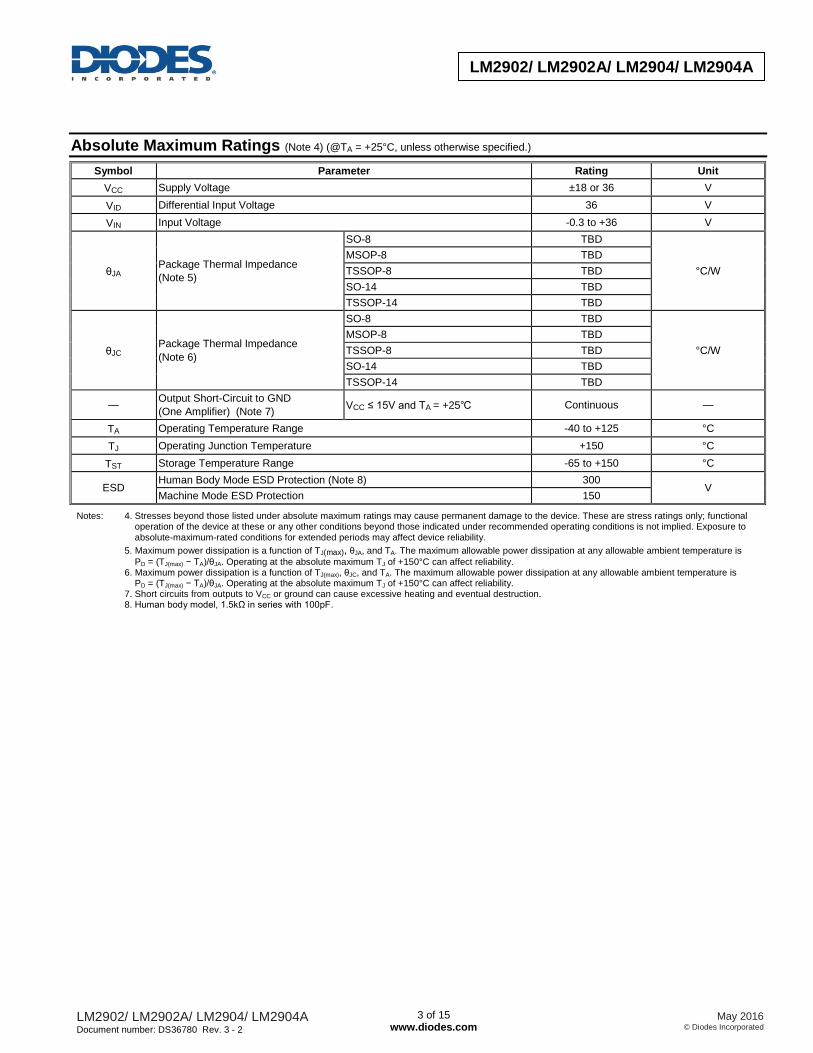
Absolute Maximum Ratings (Note 4) (@TA = +25°C, unless otherwise specified.)
Symbol Parameter Rating Unit
VCC Supply Voltage ±18 or 36 V
VID Differential Input Voltage 36 V
VIN Input Voltage -0.3 to +36 V
θJA Package Thermal Impedance
(Note 5)
SO-8 TBD
°C/W
MSOP-8 TBD
TSSOP-8 TBD
SO-14 TBD
TSSOP-14 TBD
θJC Package Thermal Impedance
(Note 6)
SO-8 TBD
°C/W
MSOP-8 TBD
TSSOP-8 TBD
SO-14 TBD
TSSOP-14 TBD
— Output Short-Circuit to GND
(One Amplifier) (Note 7) VCC ≤ 15V and TA = +25 Continuous —
TA Operating Temperature Range -40 to +125 °C
TJ Operating Junction Temperature +150 °C
TST Storage Temperature Range -65 to +150 °C
ESD Human Body Mode ESD Protection (Note 8) 300
V Machine Mode ESD Protection 150
Notes: 4. Stresses beyond those listed under absolute maximum ratings may cause permanent damage to the device. These are stress ratings only; functional operation of the device at these or any other conditions beyond those indicated under recommended operating conditions is not implied. Exposure to absolute-maximum-rated conditions for extended periods may affect device reliability.
5. Maximum power dissipation is a function of TJ(max), θJA, and TA. The maximum allowable power dissipation at any allowable ambient temperature is
PD = (TJ(max) − TA)/θJA. Operating at the absolute maximum TJ of +150°C can affect reliability. 6. Maximum power dissipation is a function of TJ(max), θJC, and TA. The maximum allowable power dissipation at any allowable ambient temperature is PD = (TJ(max) − TA)/θJA. Operating at the absolute maximum TJ of +150°C can affect reliability. 7. Short circuits from outputs to VCC or ground can cause excessive heating and eventual destruction. 8. Human body model, 1.5kΩ in series with 100pF.
LM2902/ LM2902A/ LM2904/ LM2904A Document number: DS36780 Rev. 3 - 2
4 of 15 www.diodes.com
May 2016 © Diodes Incorporated
LM2902/ LM2902A/ LM2904/ LM2904A
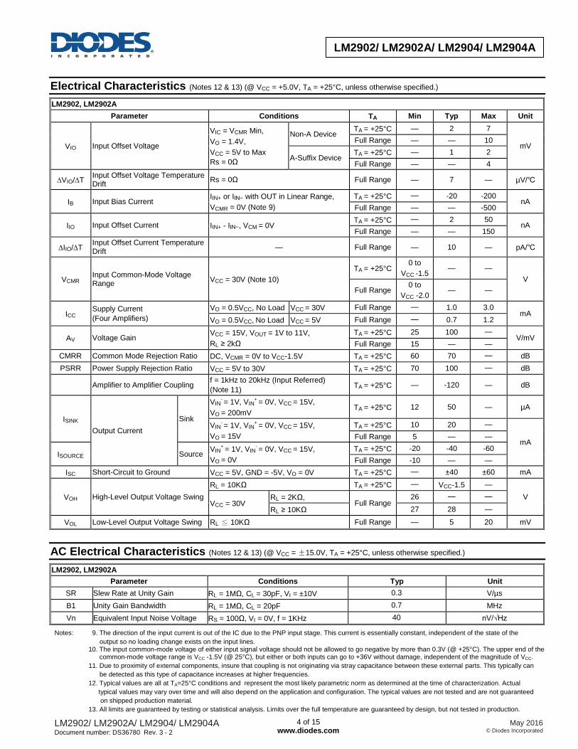
Electrical Characteristics (Notes 12 & 13) (@ VCC = +5.0V, TA = +25°C, unless otherwise specified.)
LM2902, LM2902A
Parameter Conditions TA Min Typ Max Unit
VIO Input Offset Voltage
VIC = VCMR Min,
VO = 1.4V,
VCC = 5V to Max
Rs = 0Ω
Non-A Device TA = +25°C — 2 7
mV Full Range — — 10
A-Suffix Device TA = +25°C — 1 2
Full Range — — 4
∆VIO/∆T Input Offset Voltage Temperature Drift
Rs = 0Ω Full Range — 7 — µV/
IB Input Bias Current IIN+ or IIN− with OUT in Linear Range,
VCMR = 0V (Note 9)
TA = +25°C — -20 -200 nA
Full Range — — -500
IIO Input Offset Current IIN+ - IIN−, VCM = 0V TA = +25°C — 2 50
nA Full Range — — 150
∆IIO/∆T Input Offset Current Temperature Drift
— Full Range — 10 — pA/
VCMR Input Common-Mode Voltage Range
VCC = 30V (Note 10)
TA = +25°C 0 to
VCC -1.5
— —
V
Full Range 0 to
VCC -2.0 — —
ICC Supply Current
(Four Amplifiers)
VO = 0.5VCC, No Load VCC = 30V Full Range — 1.0 3.0
mA VO = 0.5VCC, No Load VCC
= 5V Full Range — 0.7 1.2
AV Voltage Gain VCC = 15V, VOUT = 1V to 11V,
RL ≥ 2kΩ
TA = +25°C 25 100 — V/mV
Full Range 15 — —
CMRR Common Mode Rejection Ratio DC, VCMR = 0V to VCC-1.5V TA = +25°C 60 70 — dB
PSRR Power Supply Rejection Ratio VCC = 5V to 30V TA = +25°C 70 100 — dB
Amplifier to Amplifier Coupling f = 1kHz to 20kHz (Input Referred)
(Note 11) TA = +25°C — -120 — dB
ISINK
Output Current
Sink
VIN- = 1V, VIN
+ = 0V, VCC
= 15V,
VO = 200mV TA = +25°C 12 50 — µA
VIN- = 1V, VIN
+ = 0V, VCC
= 15V,
VO = 15V
TA = +25°C 10 20 —
mA Full Range 5 — —
ISOURCE Source VIN
+ = 1V, VIN
- = 0V, VCC
= 15V,
VO = 0V
TA = +25°C -20 -40 -60
Full Range -10 — —
ISC Short-Circuit to Ground VCC = 5V, GND = -5V, VO = 0V TA = +25°C — ±40 ±60 mA
VOH High-Level Output Voltage Swing
RL = 10KΩ TA = +25°C — VCC-1.5 —
V VCC = 30V
RL = 2KΩ, Full Range
26 — —
RL ≥ 10KΩ 27 28 —
VOL Low-Level Output Voltage Swing RL ≦ 10KΩ Full Range — 5 20 mV
AC Electrical Characteristics (Notes 12 & 13) (@ VCC = ±15.0V, TA = +25°C, unless otherwise specified.)
LM2902, LM2902A
Parameter Conditions Typ Unit
SR Slew Rate at Unity Gain RL = 1MΩ, CL = 30pF, VI = ±10V 0.3 V/µs
B1 Unity Gain Bandwidth RL = 1MΩ, CL = 20pF 0.7 MHz
Vn Equivalent Input Noise Voltage RS = 100Ω, VI = 0V, f = 1KHz 40 nV/√Hz
Notes: 9. The direction of the input current is out of the IC due to the PNP input stage. This current is essentially constant, independent of the state of the
output so no loading change exists on the input lines. 10. The input common-mode voltage of either input signal voltage should not be allowed to go negative by more than 0.3V (@ +25°C). The upper end of the common-mode voltage range is VCC -1.5V (@ 25°C), but either or both inputs can go to +36V without damage, independent of the magnitude of VCC.
11. Due to proximity of external components, insure that coupling is not originating via stray capacitance between these external parts. This typically can
be detected as this type of capacitance increases at higher frequencies.
12. Typical values are all at TA=25°C conditions and represent the most likely parametric norm as determined at the time of characterization. Actual
typical values may vary over time and will also depend on the application and configuration. The typical values are not tested and are not guaranteed
on shipped production material.
13. All limits are guaranteed by testing or statistical analysis. Limits over the full temperature are guaranteed by design, but not tested in production.
LM2902/ LM2902A/ LM2904/ LM2904A Document number: DS36780 Rev. 3 - 2
5 of 15 www.diodes.com
May 2016 © Diodes Incorporated
LM2902/ LM2902A/ LM2904/ LM2904A
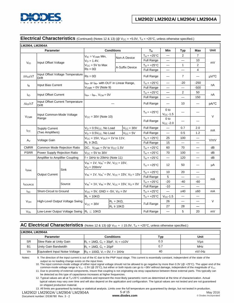
Electrical Characteristics (Continued) (Notes 12 & 13) (@ VCC = +5.0V, TA = +25°C, unless otherwise specified.)
LM2904, LM2904A
Parameter Conditions TA Min Typ Max Unit
VIO Input Offset Voltage
VIC = VCMR Min,
VO = 1.4V,
VCC = 5V to Max
Rs = 0Ω
Non-A Device TA = +25°C — 2 7
mV Full Range — — 10
A-Suffix Device TA = +25°C — 1 2
Full Range — — 4
∆VIO/∆T Input Offset Voltage Temperature Drift
Rs = 0Ω Full Range — 7 — µV/
IB Input Bias Current IIN+ or IIN− with OUT in Linear Range,
VCMR = 0V (Note 9)
TA = +25°C — -20 -250 nA
Full Range — — -500
IIO Input Offset Current IIN+ - IIN−, VCM = 0V TA = +25°C — 2 50
nA Full Range — — 150
∆IIO/∆T Input Offset Current Temperature Drift
— Full Range — 10 — pA/
VCMR Input Common-Mode Voltage Range
VCC = 30V (Note 10)
TA = +25°C 0 to
VCC -1.5
— —
V
Full Range 0 to
VCC -2.0 — —
ICC Supply Current
(Two Amplifiers)
VO = 0.5VCC, No Load VCC = 30V Full Range — 0.7 2.0
mA VO = 0.5VCC, No Load VCC
= 5V Full Range — 0.5 1.2
AV Voltage Gain VCC = 15V, VOUT = 1V to 11V,
RL ≥ 2kΩ,
TA = +25°C 25 100 — V/mV
Full Range 15 — —
CMRR Common Mode Rejection Ratio DC,VCMR = 0V to VCC-1.5V TA = +25°C 60 70 — dB
PSRR Power Supply Rejection Ratio VCC = 5V to 30V TA = +25°C 70 100 — dB
Amplifier to Amplifier Coupling f = 1kHz to 20kHz (Note 11) TA = +25°C — 120 — dB
ISINK
Output Current
Sink
VIN- = 1V, VIN
+ = 0V, VCC
= 15V,
VO = 200mV TA = +25°C 12 50 — µA
VIN- = 1V, VIN
+ = 0V, VCC
= 15V, VO = 15V
TA = +25°C 10 20 —
mA Full Range 5 — —
ISOURCE Source VIN+ = 1V, VIN
- = 0V, VCC
= 15V, VO = 0V
TA = +25°C -20 -40 -60
Full Range -10 — —
ISC Short-Circuit to Ground VCC = 5V, GND = -5V, VO = 0V TA = +25°C — ±40 ±60 mA
VOH High-Level Output Voltage Swing
RL = 10KΩ TA = +25°C VCC-1.5 — —
V VCC = 30V
RL = 2KΩ, Full Range
26 — —
RL ≥ 10KΩ 27 28 —
VOL Low-Lever Output Voltage Swing RL ≦ 10KΩ Full Range — 5 20 mV
AC Electrical Characteristics (Notes 12 & 13) (@ VCC = ±15.0V, TA = +25°C, unless otherwise specified.)
LM2904, LM2904A
Parameter Conditions Typ Unit
SR Slew Rate at Unity Gain RL = 1MΩ, CL = 30pF, VI = ±10V 0.3 V/µs
B1 Unity Gain Bandwidth RL = 1MΩ, CL = 20pF 0.7 MHz
Vn Equivalent Input Noise Voltage RS = 100Ω, VI = 0V, f = 1KHz 40 nV/√Hz
Notes: 9. The direction of the input current is out of the IC due to the PNP input stage. This current is essentially constant, independent of the state of the
output so no loading change exists on the input lines. 10. The input common-mode voltage of either input signal voltage should not be allowed to go negative by more than 0.3V (@ +25°C). The upper end of the common-mode voltage range is VCC -1.5V (@ 25°C), but either or both inputs can go to +36V without damage, independent of the magnitude of VCC.
11. Due to proximity of external components, insure that coupling is not originating via stray capacitance between these external parts. This typically can
be detected as this type of capacitance increases at higher frequencies.
12. Typical values are all at TA=25°C conditions and represent the most likely parametric norm as determined at the time of characterization. Actual
typical values may vary over time and will also depend on the application and configuration. The typical values are not tested and are not guaranteed
on shipped production material.
13. All limits are guaranteed by testing or statistical analysis. Limits over the full temperature are guaranteed by design, but not tested in production.
LM2902/ LM2902A/ LM2904/ LM2904A Document number: DS36780 Rev. 3 - 2
6 of 15 www.diodes.com
May 2016 © Diodes Incorporated
LM2902/ LM2902A/ LM2904/ LM2904A
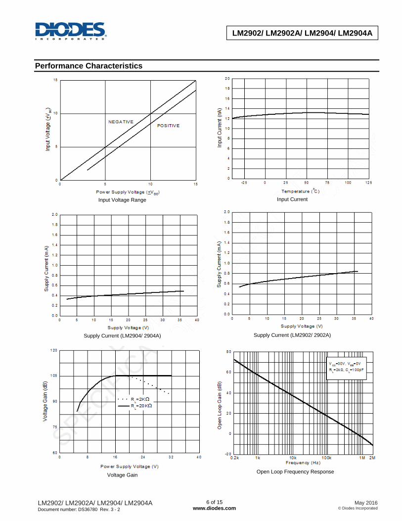
Performance Characteristics
Input Voltage Range
Input Current
Supply Current (LM2904/ 2904A)
Supply Current (LM2902/ 2902A)
Voltage Gain
Open Loop Frequency Response
LM2902/ LM2902A/ LM2904/ LM2904A Document number: DS36780 Rev. 3 - 2
7 of 15 www.diodes.com
May 2016 © Diodes Incorporated
LM2902/ LM2902A/ LM2904/ LM2904A
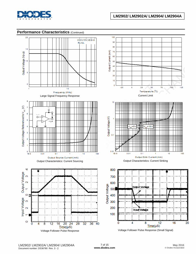
Performance Characteristics (Continued)
Large Signal Frequency Response
Current Limit
Output Characteristics: Current Sourcing
Output Characteristics: Current Sinking
Voltage Follower Pulse Response
Voltage Follower Pulse Response (Small Signal)
LM2902/ LM2902A/ LM2904/ LM2904A Document number: DS36780 Rev. 3 - 2
8 of 15 www.diodes.com
May 2016 © Diodes Incorporated
LM2902/ LM2902A/ LM2904/ LM2904A
Application Information
General Information
The LM2902/2904 series are op amps which operate with only a single power supply voltage, have true-differential inputs, and remain in the linear
mode with an input common-mode voltage of 0VDC. These amplifiers operate over a wide range of power supply voltage with little change in
performance characteristics. At +25°C amplifier operation is possible down to a minimum supply voltage of 2.3VDC.
Precautions should be taken to insure that the power supply for the integrated circuit never becomes reversed in polarity or that the unit is not
inadvertently installed backwards in a test socket as an unlimited current surge through the resulting forward diode within the IC could cause fusing
of the internal conductors and result in a destroyed unit.
Large differential input voltages can be easily accommodated and, as input differential voltage protection diodes are not needed, no large input
currents result from large differential input voltages. The differential input voltage may be larger than V+ without damaging the device. Protection
should be provided to prevent the input voltages from going negative more than -0.3VDC (@ +25°C). An input clamp diode with a resistor to the IC
input terminal can be used.
To reduce the power supply current drain, the amplifiers have a Class A output stage for small signal levels which converts to Class B in a large
signal mode. These allow the amplifiers to both source and sink large output currents. Therefore both NPN and PNP external current boost
transistors can be used to extend the power capability of the basic amplifiers. The output voltage needs to raise approximately 1 diode drop above
ground to bias the on-chip vertical PNP transistor for output current sinking applications.
For AC applications, where the load is capacitive coupled to the output of the amplifier, a resistor should be used, from the output of the amplifier to
ground to increase the Class A bias current and prevent crossover distortion. Where the load is directly coupled, as in DC applications, there is no
crossover distortion.
Capacitive loads which are applied directly to the output of the amplifier reduce the loop stability margin. Values of 50pF can be accommodated
using the worst-case non-inverting unity gain connection. Large closed loop gains or resistive isolation should be used if larger load capacitance
must be driven by the amplifier.
The bias network of the LM2902/2904 series establishes a quiescent current which is independent of the magnitude of the power supply voltage
over the range of 3VDC to 30VDC.
Output short circuits either to ground or to the positive power supply should be of short time duration. Units can be destroyed, not as a result of the
short circuit current causing metal fusing, but rather due to the large increase in IC chip dissipation which will cause eventual failure due to
excessive function temperatures. Putting direct short-circuits on more than one amplifier at a time will increase the total IC power dissipation to
destructive levels, if not properly protected with external dissipation limiting resistors in series with the output leads of the amplifiers. The larger
value of output source current which is available at +25°C provides a larger output current capability at elevated temperatures (see typical
performance characteristics) than a standard IC op amp.
The circuits presented in the section on typical applications emphasize operation on only a single power supply voltage. If complementary power
supplies are available, all of the standard op amp circuits can be used. In general, introducing a pseudo-ground (a bias voltage reference of VCC/2)
will allow operation above and below this value in single power supply systems. Many application circuits are shown which take advantage of the
wide input common-mode voltage range which includes ground. In most cases, input biasing is not required and input voltages which range to
ground can easily be accommodated.

LM2902/ LM2902A/ LM2904/ LM2904A Document number: DS36780 Rev. 3 - 2
9 of 15 www.diodes.com
May 2016 © Diodes Incorporated
LM2902/ LM2902A/ LM2904/ LM2904A
Application Information (Continued)
Power Supply Bypassing and Layout
The LM29xx family operate both single supply voltage range 3V to 36V or dual supply voltage ±1.5V to ±18V.
As with any operation amplifier, proper supply bypassing is critical for low noise performance and high power supply rejection. For single supply
operation system, a minimum 0.1µF bypass capacitor should be recommended to place as close as possible between the VCC Pin and GND. For
dual supply operation, both the positive supply pin and negative supply pin should be bypassed to ground with a separate 0.1µF ceramic capacitor.
2.2µF tantalum capacitor can be added for better performance. Keep the length of leads and traces that connect capacitors between the LM29xx
power supply pin and ground as short as possible.
Ordering Information (Note 14)
LM290X X XXX - 13
Channel Grade
3 : Dual
PackingPackage
S : SO-8
13 : Tape & Reel
1 : QuadA : Low VIO
Blank : NormalS14 : SO-14T14 : TSSOP-14
M8: MSOP-8
TH: TSSOP-8
Part Number Package Code Packaging 13” Tape and Reel
Quantity Part Number Suffix
LM2902T14-13 T14 TSSOP-14 2,500/Tape & Reel -13
LM2902AT14-13 T14 TSSOP-14 2,500/Tape & Reel -13
LM2902S14-13 S14 SO-14 2,500/Tape & Reel -13
LM2902AS14-13 S14 SO-14 2,500/Tape & Reel -13
LM2904S-13 S SO-8 2,500/Tape & Reel -13
LM2904AS-13 S SO-8 2,500/Tape & Reel -13
LM2904AM8-13 M8 MSOP-8 2,500/Tape & Reel -13
LM2904M8-13 M8 MSOP-8 2,500/Tape & Reel -13
LM2904ATH-13 TH TSSOP-8 2,500/Tape & Reel -13
LM2904TH-13 TH TSSOP-8 2,500/Tape & Reel -13
Note: 14. For packaging details, go to our website at http://www.diodes.com/products/packages.html
LM2902/ LM2902A/ LM2904/ LM2904A Document number: DS36780 Rev. 3 - 2
10 of 15 www.diodes.com
May 2016 © Diodes Incorporated
LM2902/ LM2902A/ LM2904/ LM2904A
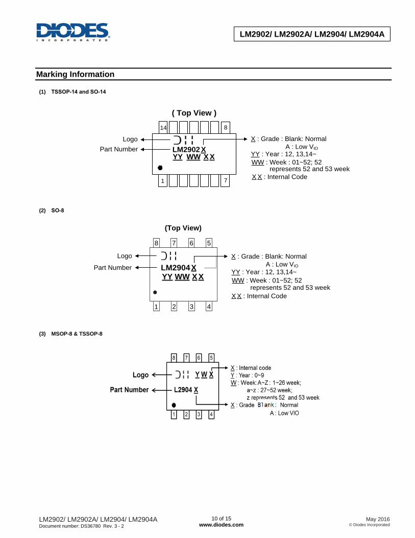
Marking Information
(1) TSSOP-14 and SO-14
( Top View )
1
LM2902XYY WW X X
Logo
14
Part Number
8
7
WW : Week : 01~52; 52
YY : Year : 12, 13,14~
X X : Internal Code
represents 52 and 53 week
X : Grade : Blank: Normal
A : Low VIO
(2) SO-8
LM2904X
(Top View)
YY WW X X
Part Number
Logo X : Grade : Blank: Normal
A : Low VIO
8 7 6 5
1 2 3 4
WW : Week : 01~52; 52
YY : Year : 12, 13,14~
X X : Internal Code
represents 52 and 53 week
(3) MSOP-8 & TSSOP-8
LM2902/ LM2902A/ LM2904/ LM2904A Document number: DS36780 Rev. 3 - 2
11 of 15 www.diodes.com
May 2016 © Diodes Incorporated
LM2902/ LM2902A/ LM2904/ LM2904A
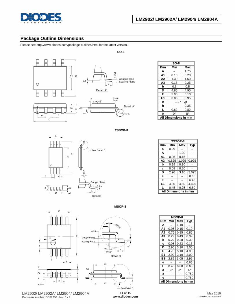
Package Outline Dimensions
Please see http://www.diodes.com/package-outlines.html for the latest version.
SO-8
SO-8
Dim Min Max
A 1.75
A1 0.10 0.20
A2 1.30 1.50
A3 0.15 0.25
b 0.3 0.5
D 4.85 4.95
E 5.90 6.10
E1 3.85 3.95
e 1.27 Typ
h 0.35
L 0.62 0.82
0° 8°
All Dimensions in mm
TSSOP-8
TSSOP-8
Dim Min Max Typ
a 0.09
A 1.20
A1 0.05 0.15
A2 0.825 1.025 0.925
b 0.19 0.30
c 0.09 0.20
D 2.90 3.10 3.025
e 0.65
E 6.40
E1 4.30 4.50 4.425
L 0.45 0.75 0.60
All Dimensions in mm
MSOP-8
MSOP-8
Dim Min Max Typ
A 1.10
A1 0.05 0.15 0.10
A2 0.75 0.95 0.86
A3 0.29 0.49 0.39
b 0.22 0.38 0.30
c 0.08 0.23 0.15
D 2.90 3.10 3.00
E 4.70 5.10 4.90
E1 2.90 3.10 3.00
E3 2.85 3.05 2.95
e 0.65
L 0.40 0.80 0.60
a 0° 8° 4°
x 0.750
y 0.750
All Dimensions in mm
Gauge PlaneSeating Plane
Detail ‘A’
Detail ‘A’
EE1
h
L
D
e b
A2
A1
A
45°
7°~9°
A3
0.2
54
A
A1
A2
e
Seating Plane
Gauge Plane
0.25
L
4X10°
4X10°
See Detail C
Detail C
c
a
E1
E3
A3
1
E
y
x
D
b
L
Gauge plane
See Detail C
D
E
A1
A2A
e
a
Detail C
E1
b
D
c

LM2902/ LM2902A/ LM2904/ LM2904A Document number: DS36780 Rev. 3 - 2
12 of 15 www.diodes.com
May 2016 © Diodes Incorporated
LM2902/ LM2902A/ LM2904/ LM2904A
Package Outline Dimensions (Continued)
Please see http://www.diodes.com/package-outlines.html for the latest version.
SO-14
SO-14
Dim Min Max
A 1.47 1.73
A1 0.10 0.25
A2 1.45 Typ
B 0.33 0.51
D 8.53 8.74
E 3.80 3.99
e 1.27 Typ
H 5.80 6.20
L 0.38 1.27
0° 8°
All Dimensions in mm
TSSOP-14
TSSOP-14
Dim Min Max
a1 7° (4X)
a2 0° 8°
A 4.9 5.10
B 4.30 4.50
C 1.2
D 0.8 1.05
F 1.00 Typ
F1 0.45 0.75
G 0.65 Typ
K 0.19 0.30
L 6.40 Typ
All Dimensions in mm
E H
AA2
e
D
A1
L
Gauge Plane
Detail “A”
Detail “A”
7°(4x)
B
G
L
A
K
a1 D
C
a2
F
F1
Pin# 1 Indent
Detail ‘A’
Detail ‘A’
0.25
Gauge PlaneSeating Plane
B
LM2902/ LM2902A/ LM2904/ LM2904A Document number: DS36780 Rev. 3 - 2
13 of 15 www.diodes.com
May 2016 © Diodes Incorporated
LM2902/ LM2902A/ LM2904/ LM2904A
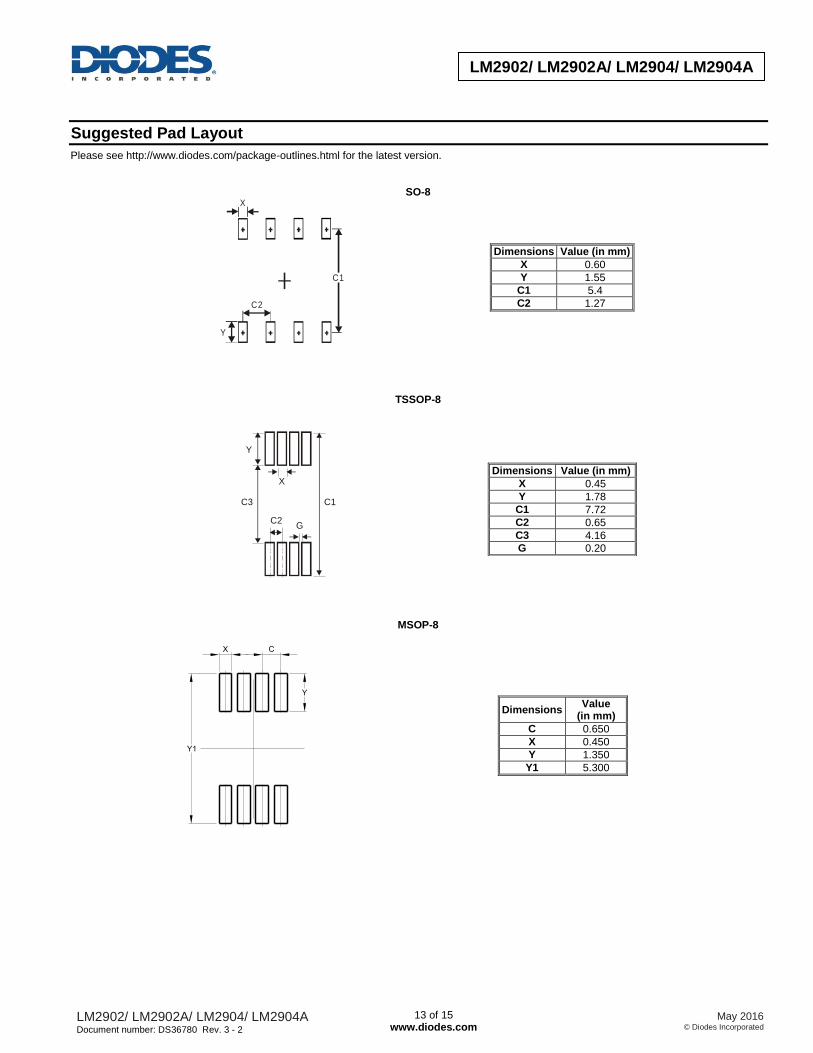
Suggested Pad Layout
Please see http://www.diodes.com/package-outlines.html for the latest version.
SO-8
Dimensions Value (in mm)
X 0.60
Y 1.55
C1 5.4
C2 1.27
TSSOP-8
Dimensions Value (in mm)
X 0.45
Y 1.78
C1 7.72
C2 0.65
C3 4.16
G 0.20
MSOP-8
Dimensions Value
(in mm)
C 0.650
X 0.450
Y 1.350
Y1 5.300
X
C1
C2
Y
X C
Y
Y1
Y
C3 C1
X
C2G
LM2902/ LM2902A/ LM2904/ LM2904A Document number: DS36780 Rev. 3 - 2
14 of 15 www.diodes.com
May 2016 © Diodes Incorporated
LM2902/ LM2902A/ LM2904/ LM2904A
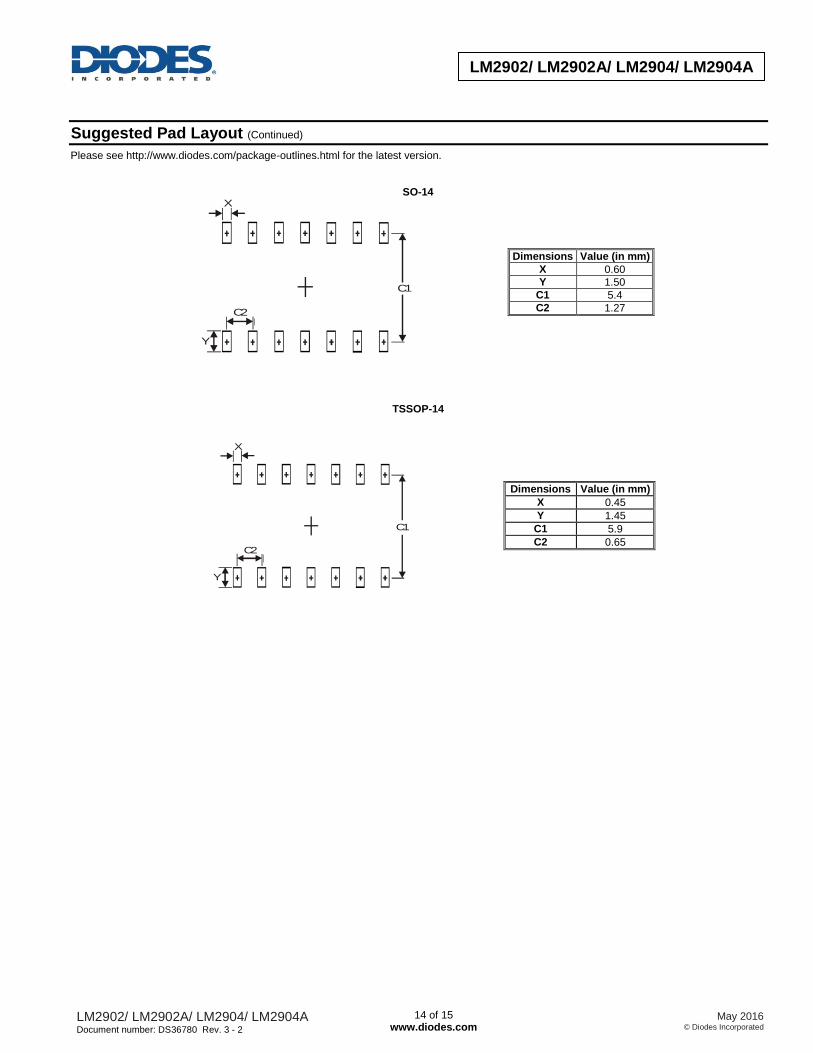
Suggested Pad Layout (Continued)
Please see http://www.diodes.com/package-outlines.html for the latest version.
SO-14
Dimensions Value (in mm)
X 0.60
Y 1.50
C1 5.4
C2 1.27
TSSOP-14
Dimensions Value (in mm)
X 0.45
Y 1.45
C1 5.9
C2 0.65
X
C1
C2
Y
X
C1
C2
Y
LM2902/ LM2902A/ LM2904/ LM2904A Document number: DS36780 Rev. 3 - 2
15 of 15 www.diodes.com
May 2016 © Diodes Incorporated
LM2902/ LM2902A/ LM2904/ LM2904A
IMPORTANT NOTICE DIODES INCORPORATED MAKES NO WARRANTY OF ANY KIND, EXPRESS OR IMPLIED, WITH REGARDS TO THIS DOCUMENT, INCLUDING, BUT NOT LIMITED TO, THE IMPLIED WARRANTIES OF MERCHANTABILITY AND FITNESS FOR A PARTICULAR PURPOSE (AND THEIR EQUIVALENTS UNDER THE LAWS OF ANY JURISDICTION). Diodes Incorporated and its subsidiaries reserve the right to make modifications, enhancements, improvements, corrections or other changes without further notice to this document and any product described herein. Diodes Incorporated does not assume any liability arising out of the application or use of this document or any product described herein; neither does Diodes Incorporated convey any license under its patent or trademark rights, nor the rights of others. Any Customer or user of this document or products described herein in such applications shall assume all risks of such use and will agree to hold Diodes Incorporated and all the companies whose products are represented on Diodes Incorporated website, harmless against all damages. Diodes Incorporated does not warrant or accept any liability whatsoever in respect of any products purchased through unauthorized sales channel. Should Customers purchase or use Diodes Incorporated products for any unintended or unauthorized application, Customers shall indemnify and hold Diodes Incorporated and its representatives harmless against all claims, damages, expenses, and attorney fees arising out of, directly or indirectly, any claim of personal injury or death associated with such unintended or unauthorized application. Products described herein may be covered by one or more United States, international or foreign patents pending. Product names and markings noted herein may also be covered by one or more United States, international or foreign trademarks. This document is written in English but may be translated into multiple languages for reference. Only the English version of this document is the final and determinative format released by Diodes Incorporated.
LIFE SUPPORT Diodes Incorporated products are specifically not authorized for use as critical components in life support devices or systems without the express written approval of the Chief Executive Officer of Diodes Incorporated. As used herein: A. Life support devices or systems are devices or systems which: 1. are intended to implant into the body, or
2. support or sustain life and whose failure to perform when properly used in accordance with instructions for use provided in the labeling can be reasonably expected to result in significant injury to the user.
B. A critical component is any component in a life support device or system whose failure to perform can be reasonably expected to cause the failure of the life support device or to affect its safety or effectiveness. Customers represent that they have all necessary expertise in the safety and regulatory ramifications of their life support devices or systems, and acknowledge and agree that they are solely responsible for all legal, regulatory and safety-related requirements concerning their products and any use of Diodes Incorporated products in such safety-critical, life support devices or systems, notwithstanding any devices- or systems-related information or support that may be provided by Diodes Incorporated. Further, Customers must fully indemnify Diodes Incorporated and its representatives against any damages arising out of the use of Diodes Incorporated products in such safety-critical, life support devices or systems. Copyright © 2016, Diodes Incorporated www.diodes.com