Embed Size (px)
Citation preview
SENSOR
+ -+
-
ADC
PRESSURE
EMI HARDENED
EMI HARDENED
+
-
V+
R1
R2
INTERFERING
RF SOURCES
NO RF RELATED
DISTURBANCES
LMV831, LMV832, LMV834
www.ti.com SNOSAZ6B –AUGUST 2008–REVISED MARCH 2013
LMV831 Single/ LMV832 Dual/ LMV834 Quad 3.3 MHz Low Power CMOS, EMI HardenedOperational Amplifiers
Check for Samples: LMV831, LMV832, LMV834
1FEATURES DESCRIPTIONTI’s LMV831, LMV832, and LMV834 are CMOS input,
2• Unless Otherwise Noted, Typical Values at TA=low power op amp IC's, providing a low input bias25°C, V+ = 3.3Vcurrent, a wide temperature range of −40°C to 125°C
• Supply Voltage 2.7V to 5.5V and exceptional performance making them robust• Supply Current (per Channel) 240 µA general purpose parts. Additionally, the
LMV831/LMV832/LMV834 are EMI hardened to• Input Offset Voltage 1 mV Maxminimize any interference so they are ideal for EMI
• Input Bias Current 0.1 pA sensitive applications.• GBW 3.3 MHz
The unity gain stable LMV831/LMV832/LMV834• EMIRR at 1.8 GHz 120 dB feature 3.3 MHz of bandwidth while consuming only• Input Noise Voltage at 1 kHz 12 nV/√Hz 0.24 mA of current per channel. These parts also
maintain stability for capacitive loads as large as 200• Slew Rate 2 V/µspF. The LMV831/LMV832/LMV834 provide superior
• Output Voltage Swing Rail-to-Rail performance and economy in terms of power and• Output Current Drive 30 mA space usage.• Operating Ambient Temperature Range −40°C This family of parts has a maximum input offset
to 125°C voltage of 1 mV, a rail-to-rail output stage and aninput common-mode voltage range that includes
APPLICATIONS ground. Over an operating range from 2.7V to 5.5Vthe LMV831/LMV832/LMV834 provide a PSRR of 93• Photodiode PreampdB, and a CMRR of 91 dB. The LMV831 is offered in
• Piezoelectric Sensors the space saving 5-Pin SC70 package, the LMV832in the 8-Pin VSSOP and the LMV834 is offered in the• Portable/Battery-Powered Electronic14-Pin TSSOP package.Equipment
• Filters/Buffers• PDAs/Phone Accessories
Typical Application
Figure 1. EMI Hardened Sensor Application1
Please be aware that an important notice concerning availability, standard warranty, and use in critical applications ofTexas Instruments semiconductor products and disclaimers thereto appears at the end of this data sheet.
2All trademarks are the property of their respective owners.
PRODUCTION DATA information is current as of publication date. Copyright © 2008–2013, Texas Instruments IncorporatedProducts conform to specifications per the terms of the TexasInstruments standard warranty. Production processing does notnecessarily include testing of all parameters.

LMV831, LMV832, LMV834
SNOSAZ6B –AUGUST 2008–REVISED MARCH 2013 www.ti.com
These devices have limited built-in ESD protection. The leads should be shorted together or the device placed in conductive foamduring storage or handling to prevent electrostatic damage to the MOS gates.
Absolute Maximum Ratings (1) (2)
Human Body Model 2 kV
ESD Tolerance (3) Charge-Device Model 1 kV
Machine Model 200V
VIN Differential ± Supply Voltage
Supply Voltage (VS = V+ – V−) 6V
V++0.4V,Voltage at Input/Output Pins V− −0.4V
Storage Temperature Range −65°C to 150°C
Junction Temperature (4) 150°C
Soldering Information Infrared or Convection (20 sec) 260°C
(1) Absolute Maximum Ratings indicate limits beyond which damage to the device may occur. Operating Ratings indicate conditions forwhich the device is intended to be functional, but specific performance is not ensured. For ensured specifications and the testconditions, see the Electrical Characteristics Tables.
(2) If Military/Aerospace specified devices are required, please contact the Texas Instruments Sales Office/ Distributors for availability andspecifications.
(3) Human Body Model, applicable std. MIL-STD-883, Method 3015.7. Machine Model, applicable std. JESD22-A115-A (ESD MM std. ofJEDEC) Field-Induced Charge-Device Model, applicable std. JESD22-C101-C (ESD FICDM std. of JEDEC).
(4) The maximum power dissipation is a function of TJ(MAX), θJA, and TA. The maximum allowable power dissipation at any ambienttemperature is PD = (TJ(MAX) - TA)/ θJA . All numbers apply for packages soldered directly onto a PC board.
Operating Ratings (1)
Temperature Range (2) −40°C to 125°C
Supply Voltage (VS = V+ – V−) 2.7V to 5.5V
5-Pin SC70 302°C/W
Package Thermal Resistance (θJA(2)) 8-Pin VSSOP 217°C/W
14-Pin TSSOP 135°C/W
(1) Absolute Maximum Ratings indicate limits beyond which damage to the device may occur. Operating Ratings indicate conditions forwhich the device is intended to be functional, but specific performance is not ensured. For ensured specifications and the testconditions, see the Electrical Characteristics Tables.
(2) The maximum power dissipation is a function of TJ(MAX), θJA, and TA. The maximum allowable power dissipation at any ambienttemperature is PD = (TJ(MAX) - TA)/ θJA . All numbers apply for packages soldered directly onto a PC board.
3.3V Electrical Characteristics (1)
Unless otherwise specified, all limits are specified for at TA = 25°C, V+ = 3.3V, V− = 0V, VCM = V+/2, and RL =10 kΩ to V+/2.Boldface limits apply at the temperature extremes.
Symbol Parameter Conditions Min Typ Max Units(2) (3) (2)
VOS Input Offset Voltage (4) ±0.25 ±1.00 mV±1.23
TCVOS Input Offset Voltage Temperature LMV831, ±0.5 ±1.5Drift (4) (5) LMV832 μV/°C
LMV834 ±0.5 ±1.7
(1) Electrical Table values apply only for factory testing conditions at the temperature indicated. Factory testing conditions result in verylimited self-heating of the device such that TJ = TA. No specification of parametric performance is indicated in the electrical tables underconditions of internal self-heating where TJ > TA.
(2) Limits are 100% production tested at 25°C. Limits over the operating temperature range are specified through correlations usingstatistical quality control (SQC) method.
(3) Typical values represent the most likely parametric norm as determined at the time of characterization. Actual typical values may varyover time and will also depend on the application and configuration. The typical values are not tested and are not ensured on shippedproduction material.
(4) The typical value is calculated by applying absolute value transform to the distribution, then taking the statistical average of the resultingdistribution.
(5) This parameter is specified by design and/or characterization and is not tested in production.
2 Submit Documentation Feedback Copyright © 2008–2013, Texas Instruments Incorporated
Product Folder Links: LMV831 LMV832 LMV834

LMV831, LMV832, LMV834
www.ti.com SNOSAZ6B –AUGUST 2008–REVISED MARCH 2013
3.3V Electrical Characteristics(1) (continued)Unless otherwise specified, all limits are specified for at TA = 25°C, V+ = 3.3V, V− = 0V, VCM = V+/2, and RL =10 kΩ to V+/2.Boldface limits apply at the temperature extremes.
Symbol Parameter Conditions Min Typ Max Units(2) (3) (2)
IB Input Bias Current (5) 0.1 10 pA500
IOS Input Offset Current 1 pA
CMRR Common-Mode Rejection Ratio (4) 0.2V ≤ VCM ≤ V+ - 1.2V 76 91 dB75
PSRR Power Supply Rejection Ratio (4) 2.7V ≤ V+ ≤ 5.5V, 76 93 dBVOUT = 1V 75
EMIRR EMI Rejection Ratio, IN+ and IN- (6) VRF_PEAK=100 mVP (−20 dBP), 80f = 400 MHz
VRF_PEAK=100 mVP (−20 dBP), 90f = 900 MHz
dBVRF_PEAK=100 mVP (−20 dBP), 110f = 1800 MHz
VRF_PEAK=100 mVP (−20 dBP), 120f = 2400 MHz
CMVR Input Common-Mode Voltage Range CMRR ≥ 65 dB −0.1 2.1 V
AVOL Large Signal Voltage Gain (7) RL = 2 kΩ, LMV831, 102 121VOUT = 0.15V to 1.65V, LMV832 102VOUT = 3.15V to 1.65V LMV834 102 121
102dB
RL = 10 kΩ, LMV831, 104 126VOUT = 0.1V to 1.65V, LMV832 104VOUT = 3.2V to 1.65V LMV834 104 123
103
VOUT Output Voltage Swing High RL = 2 kΩ to V+/2 LMV831, 29 36LMV832 43
LMV834 31 3844
RL = 10 kΩ to V+/2 LMV831, 6 8LMV832 9 mV from
either railLMV834 7 910
Output Voltage Swing Low R = 2 kΩ to V+/2 25 3443
RL = 10 kΩ to V+/2 5 810
IOUT Output Short Circuit Current Sourcing, VOUT = VCM, LMV831, 27 28VIN = 100 mV LMV832 22
LMV834 24 28 mA19
Sinking, VOUT = VCM, 27 32VIN = −100 mV 21
IS Supply Current LMV831 0.24 0.270.30
LMV832 0.46 0.51 mA0.58
LMV834 0.90 1.001.16
SR Slew Rate (8) AV = +1, VOUT = 1 VPP, 2 V/μs10% to 90%
(6) The EMI Rejection Ratio is defined as EMIRR = 20log ( VRF_PEAK/ΔVOS).(7) The specified limits represent the lower of the measured values for each output range condition.(8) Number specified is the slower of positive and negative slew rates.
Copyright © 2008–2013, Texas Instruments Incorporated Submit Documentation Feedback 3
Product Folder Links: LMV831 LMV832 LMV834

LMV831, LMV832, LMV834
SNOSAZ6B –AUGUST 2008–REVISED MARCH 2013 www.ti.com
3.3V Electrical Characteristics(1) (continued)Unless otherwise specified, all limits are specified for at TA = 25°C, V+ = 3.3V, V− = 0V, VCM = V+/2, and RL =10 kΩ to V+/2.Boldface limits apply at the temperature extremes.
Symbol Parameter Conditions Min Typ Max Units(2) (3) (2)
GBW Gain Bandwidth Product 3.3 MHz
Φm Phase Margin 65 deg
en Input Referred Voltage Noise Density f = 1 kHz 12nV/√Hz
f = 10 kHz 10
in Input Referred Current Noise Density f = 1 kHz 0.005 pA/√Hz
ROUT Closed Loop Output Impedance f = 2 MHz 500 ΩCIN Common-mode Input Capacitance 15
pFDifferential-mode Input Capacitance 20
THD+N Total Harmonic Distortion + Noise f = 1 kHz, AV = 1, BW ≥ 500 kHz 0.02 %
5V Electrical Characteristics (1)
Unless otherwise specified, all limits are specified for at TA = 25°C, V+ = 5V, V− = 0V, VCM = V+/2, and RL = 10 kΩ to V+/2.Boldface limits apply at the temperature extremes.
Symbol Parameter Conditions Min Typ Max Units(2) (3) (2)
VOS Input Offset Voltage (4) ±0.25 ±1.00 mV±1.23
TCVOS Input Offset Voltage Temperature LMV831, ±0.5 ±1.5Drift (4) (5) LMV832 μV/°C
LMV834 ±0.5 ±1.7
IB Input Bias Current (5) 0.1 10 pA500
IOS Input Offset Current 1 pA
CMRR Common-Mode Rejection Ratio (4) 0V ≤ VCM ≤ V+ −1.2V 77 93 dB77
PSRR Power Supply Rejection Ratio (4) 2.7V ≤ V+ ≤ 5.5V, 76 93 dBVOUT = 1V 75
EMIRR EMI Rejection Ratio, IN+ and IN- (6) VRF_PEAK=100 mVP (−20 dBP), 80f = 400 MHz
VRF_PEAK=100 mVP (−20 dBP), 90f = 900 MHz
dBVRF_PEAK=100 mVP (−20 dBP), 110f = 1800 MHz
VRF_PEAK=100 mVP (−20 dBP), 120f = 2400 MHz
CMVR Input Common-Mode Voltage Range CMRR ≥ 65 dB –0.1 3.8 V
(1) Electrical Table values apply only for factory testing conditions at the temperature indicated. Factory testing conditions result in verylimited self-heating of the device such that TJ = TA. No specification of parametric performance is indicated in the electrical tables underconditions of internal self-heating where TJ > TA.
(2) Limits are 100% production tested at 25°C. Limits over the operating temperature range are specified through correlations usingstatistical quality control (SQC) method.
(3) Typical values represent the most likely parametric norm as determined at the time of characterization. Actual typical values may varyover time and will also depend on the application and configuration. The typical values are not tested and are not ensured on shippedproduction material.
(4) The typical value is calculated by applying absolute value transform to the distribution, then taking the statistical average of the resultingdistribution.
(5) This parameter is specified by design and/or characterization and is not tested in production.(6) The EMI Rejection Ratio is defined as EMIRR = 20log ( VRF_PEAK/ΔVOS).
4 Submit Documentation Feedback Copyright © 2008–2013, Texas Instruments Incorporated
Product Folder Links: LMV831 LMV832 LMV834

LMV831, LMV832, LMV834
www.ti.com SNOSAZ6B –AUGUST 2008–REVISED MARCH 2013
5V Electrical Characteristics(1) (continued)Unless otherwise specified, all limits are specified for at TA = 25°C, V+ = 5V, V− = 0V, VCM = V+/2, and RL = 10 kΩ to V+/2.Boldface limits apply at the temperature extremes.
Symbol Parameter Conditions Min Typ Max Units(2) (3) (2)
AVOL Large Signal Voltage Gain (7) RL = 2 kΩ, LMV831, 107 127VOUT = 0.15V to 2.5V, LMV832 106VOUT = 4.85V to 2.5V LMV834 104 127
104dB
RL = 10 kΩ, LMV831, 107 130VOUT = 0.1V to 2.5V, LMV832 107VOUT = 4.9V to 2.5V LMV834 105 127
104
VOUT Output Voltage Swing High RL = 2 kΩ to V+/2 LMV831, 32 42LMV832 49
LMV834 35 4552
RL = 10 kΩ to V+/2 LMV831, 6 9LMV832 10 mV from
either railLMV834 7 1011
Output Voltage Swing Low RL = 2 kΩ to V+/2 27 4352
RL = 10 kΩ to V+/2 6 1012
IOUT Output Short Circuit Current Sourcing VOUT = VCM LMV831, 59 66VIN = 100 mV LMV832 49
LMV834 57 6345
mASinking VOUT = VCM LMV831, 50 64VIN = −100 mV LMV832 41
LMV834 53 6341
IS Supply Current LMV831 0.25 0.270.31
LMV832 0.47 0.52 mA0.60
LMV834 0.92 1.021.18
SR Slew Rate (8) AV = +1, VOUT = 2VPP, 2 V/μs10% to 90%
GBW Gain Bandwidth Product 3.3 MHz
Φm Phase Margin 65 deg
en Input Referred Voltage Noise f = 1 kHz 12nV/√Hz
f = 10 kHz 10
in Input Referred Current Noise f = 1 kHz 0.005 pA/√Hz
ROUT Closed Loop Output Impedance f = 2 MHz 500 ΩCIN Common-mode Input Capacitance 14
pFDifferential-mode Input Capacitance 20
THD+N Total Harmonic Distortion + Noise f = 1 kHz, AV = 1, BW ≥ 500 kHz 0.02 %
(7) The specified limits represent the lower of the measured values for each output range condition.(8) Number specified is the slower of positive and negative slew rates.
Copyright © 2008–2013, Texas Instruments Incorporated Submit Documentation Feedback 5
Product Folder Links: LMV831 LMV832 LMV834

LMV831, LMV832, LMV834
SNOSAZ6B –AUGUST 2008–REVISED MARCH 2013 www.ti.com
Connection Diagram
Figure 2. 5-Pin SC70 Figure 3. 8-Pin VSSOP Figure 4. 14-Pin TSSOPTop View Top View Top View
6 Submit Documentation Feedback Copyright © 2008–2013, Texas Instruments Incorporated
Product Folder Links: LMV831 LMV832 LMV834

VOUT (V)
VO
S (
µV
)
6
4
2
0
-2
-4
-6
0 1 2 3 4 5
V+ = 5.0V, RL = 2k
VCM (V)
I B (
pA)
5
4
3
2
1
0
-1
-2
-3
-4
-5-1 0 1 2 3 4 5 6
3.3V
5V
TA = 25°C
VSUPPLY (V)
VO
S (m
V)
0.3
0.2
0.1
0
-0.1
-0.2
-0.3
2.5 3.0 3.5 4.0 4.5 5.0 5.5 6.0
-40°C
25°C
85°C125°C
TEMPERATURE (°C)
VO
S (µ
V)
200150100
500
-50-100-150-200
-50 -25 0 25 50 75 100 125
3.3V
5.0V
VCM (V)
VO
S (m
V)
0.3
0.2
0.1
0
-0.1
-0.2
-0.3
-0.5 0.0 0.5 1.0 1.5 2.0 2.5 3.0 3.5
-40°C
25°C
85°C125°C
V+ = 3.3V
VCM (V)
VO
S (
mV
)
0.3
0.2
0.1
0
-0.1
-0.2
-0.3
-0.5 0.5 1.5 2.5 3.5 4.5 5.5
-40°C
25°C
85°C125°C
V+ = 5.0V
LMV831, LMV832, LMV834
www.ti.com SNOSAZ6B –AUGUST 2008–REVISED MARCH 2013
Typical Performance CharacteristicsAt TA = 25°C, RL = 10 kΩ, V+ = 3.3V, V− = 0V, Unless otherwise specified.
VOS vs. VCM at V+ = 3.3V VOS vs. VCM at V+ = 5.0V
Figure 5. Figure 6.
VOS vs. Supply Voltage VOS vs. Temperature
Figure 7. Figure 8.
VOS vs. VOUT Input Bias Current vs. VCM at 25°C
Figure 9. Figure 10.
Copyright © 2008–2013, Texas Instruments Incorporated Submit Documentation Feedback 7
Product Folder Links: LMV831 LMV832 LMV834
SUPPLY VOLTAGE (V)
SU
PP
LY C
UR
RE
NT
(m
A)
1.4
1.2
1.0
0.8
0.6
0.4
2.5 3.0 3.5 4.0 4.5 5.0 5.5 6.0
-40°C25°C
85°C125°C
TEMPERATURE (°C)
SU
PP
LY C
UR
RE
NT
(m
A)
0.4
0.3
0.2
0.1
-50 -25 0 25 50 75 100 125
3.3V
5.0V
SUPPLY VOLTAGE (V)
SU
PP
LY C
UR
RE
NT
(m
A)
0.4
0.3
0.2
0.1
2.5 3.0 3.5 4.0 4.5 5.0 5.5 6.0
-40°C25°C
85°C125°C
SUPPLY VOLTAGE (V)
SU
PP
LY C
UR
RE
NT
(m
A)
0.7
0.6
0.5
0.4
0.3
2.5 3.0 3.5 4.0 4.5 5.0 5.5 6.0
-40°C
25°C
85°C125°C
VCM (V)
I BIA
S (
pA)
50
40
30
20
10
0
-10
-20
-30
-40
-50-1 0 1 2 3 4 5 6
3.3V
5.0V
TA = 85°C
VCM (V)
I BIA
S (
pA)
500
400
300
200
100
0
-100
-200
-300
-400
-500-1 0 1 2 3 4 5 6
3.3V
5.0V
TA = 125°C
LMV831, LMV832, LMV834
SNOSAZ6B –AUGUST 2008–REVISED MARCH 2013 www.ti.com
Typical Performance Characteristics (continued)At TA = 25°C, RL = 10 kΩ, V+ = 3.3V, V− = 0V, Unless otherwise specified.
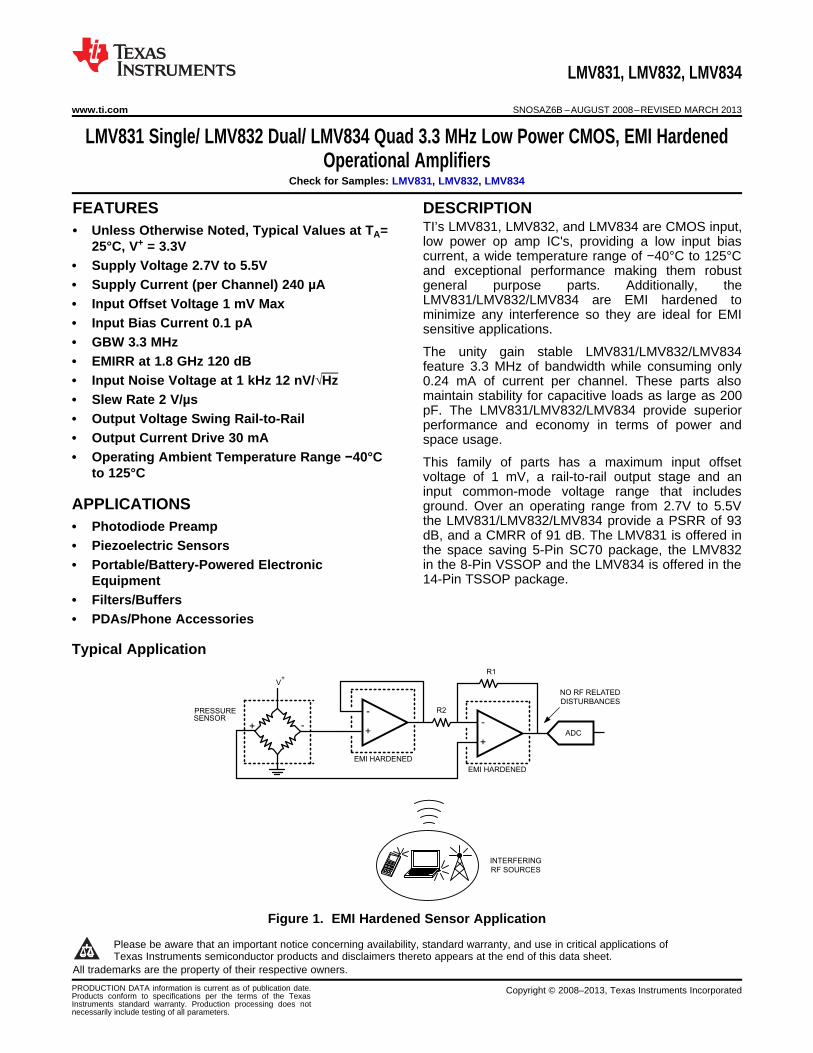
Input Bias Current vs. VCM at 85°C Input Bias Current vs. VCM at 125°C
Figure 11. Figure 12.
Supply Current vs. Supply Voltage Single LMV831 Supply Current vs. Supply Voltage Dual LMV832
Figure 13. Figure 14.
Supply Current vs. Supply Voltage Quad LMV834 Supply Current vs. Temperature Single LMV831
Figure 15. Figure 16.
8 Submit Documentation Feedback Copyright © 2008–2013, Texas Instruments Incorporated
Product Folder Links: LMV831 LMV832 LMV834

SUPPLY VOLTAGE (V)
VO
UT F
RO
M R
AIL
HIG
H (
mV
)
60
50
40
30
20
10
2.5 3.0 3.5 4.0 4.5 5.0 5.5 6.0
-40°C
25°C
85°C125°C
RL = 2k
SUPPLY VOLTAGE (V)
VO
UT F
RO
M R
AIL
HIG
H (
mV
) 12
10
8
6
4
2
0
2.5 3.0 3.5 4.0 4.5 5.0 5.5 6.0
-40°C
25°C
85°C125°C
RL = 10k
SUPPLY VOLTAGE (V)
I SIN
K (
mA
)
100908070605040302010
2.5 3.0 3.5 4.0 4.5 5.0 5.5 6.0
-40°C25°C
85°C 125°C
SUPPLY VOLTAGE (V)
I SO
UR
CE
(m
A)
100908070605040302010
2.5 3.0 3.5 4.0 4.5 5.0 5.5 6.0
-40°C
25°C
85°C
125°C
TEMPERATURE (°C)
SU
PP
LY C
UR
RE
NT
(m
A)
0.7
0.6
0.5
0.4
0.3
-50 -25 0 25 50 75 100 125
3.3V
5.0V
TEMPERATURE (°C)
SU
PP
LY C
UR
RE
NT
(m
A)
1.4
1.2
1.0
0.8
0.6
0.4
-50 -25 0 25 50 75 100 125
3.3V
5.0V
LMV831, LMV832, LMV834
www.ti.com SNOSAZ6B –AUGUST 2008–REVISED MARCH 2013
Typical Performance Characteristics (continued)At TA = 25°C, RL = 10 kΩ, V+ = 3.3V, V− = 0V, Unless otherwise specified.
Supply Current vs. Temperature Dual LMV832 Supply Current vs. Temperature Quad LMV834
Figure 17. Figure 18.
Sinking Current vs. Supply Voltage Sourcing Current vs. Supply Voltage
Figure 19. Figure 20.
Output Swing High vs. Supply Voltage RL = 2 kΩ Output Swing High vs. Supply Voltage RL = 10 kΩ
Figure 21. Figure 22.
Copyright © 2008–2013, Texas Instruments Incorporated Submit Documentation Feedback 9
Product Folder Links: LMV831 LMV832 LMV834

PH
AS
E (
°)
FREQUENCY (Hz)
GA
IN (
dB)
60
50
40
30
20
10
010k 100k 1M 10M
-40°CGAIN
PHASE
CL = 5 pF
25°C, 85°C, 125°C100
80
60
40
20
0
-20-40°C
25°C 85°C125°C
PH
AS
E (
°)
FREQUENCY (Hz)
GA
IN (
dB)
60
50
40
30
20
10
010k 100k 1M 10M
PHASE
GAIN
5 pF
100 pF
5 pF
100 pF
100
80
60
40
20
0
-20
20 pF
50 pF
CL = 5 pF20 pF50 pF100 pF
ILOAD (mA)
VO
UT
FR
OM
RA
IL (
V) 2.0
1.61.20.80.4
0-0.4-0.8-1.2-1.6-2.0
0 5 10 15 20 25 30 35 40
-40°C
SOURCE
125°C
SOURCE
-40°C
125°C
SINK
V+ = 3.3V
ILOAD (mA)
VO
UT
FR
OM
RA
IL (
V) 2.0
1.61.20.80.4
0-0.4-0.8-1.2-1.6-2.0
0 10 20 30 40 50 60 70 80
-40°C
125°C
V+ = 5.0V
SOURCE
-40°C
125°C
SINK
SUPPLY VOLTAGE (V)
VO
UT F
RO
M R
AIL
LO
W (
mV
)
60
50
40
30
20
10
2.5 3.0 3.5 4.0 4.5 5.0 5.5 6.0
-40°C
25°C
85°C
125°CRL = 2k
SUPPLY VOLTAGE (V)
VO
UT F
RO
M R
AIL
LO
W (
mV
) 12
10
8
6
4
2
0
2.5 3.0 3.5 4.0 4.5 5.0 5.5 6.0
-40°C
25°C
85°C
125°C
RL = 10k
LMV831, LMV832, LMV834
SNOSAZ6B –AUGUST 2008–REVISED MARCH 2013 www.ti.com
Typical Performance Characteristics (continued)At TA = 25°C, RL = 10 kΩ, V+ = 3.3V, V− = 0V, Unless otherwise specified.
Output Swing Low vs. Supply Voltage RL = 2 kΩ Output Swing Low vs. Supply Voltage RL = 10 kΩ
Figure 23. Figure 24.
Output Voltage Swing vs. Load Current at V+ = 3.3V Output Voltage Swing vs. Load Current at V+ = 5.0V
Figure 25. Figure 26.
Open Loop Frequency Response vs. Temperature Open Loop Frequency Response vs. Load Conditions
Figure 27. Figure 28.
10 Submit Documentation Feedback Copyright © 2008–2013, Texas Instruments Incorporated
Product Folder Links: LMV831 LMV832 LMV834

1 µs/DIV
100
mV
/DIV
f = 100 kHzAV = +1VIN = 500 mVPP
1 us/DIV
200
mV
/DIV
f = 100 kHzAV = +10VIN = 100 mVPP
FREQUENCY (Hz)
CM
RR
(dB
)
100
80
60
40
20100 1k 10k 100k 1M 10M
V+ = 3.3V, 5.0V
AC CMRR
DCCMRR
FREQUENCY (Hz)
CH
AN
NE
L S
EP
AR
AT
ION
(dB
)
160
140
120
100
80
601k 10k 100k 1M 10M
V+ = 3.3V, 5.0V
CLOAD (pF)
PH
AS
E(°)
70
60
50
40
30
20
10
0
1 10 100 1000
3.3V
5.0V
FREQUENCY (Hz)
PS
RR
(dB
)
120
100
80
60
40
20
0100 1k 10k 100k 1M 10M
3.3V
5.0V
5.0V
3.3V
+PSRR
-PSRR
LMV831, LMV832, LMV834
www.ti.com SNOSAZ6B –AUGUST 2008–REVISED MARCH 2013
Typical Performance Characteristics (continued)At TA = 25°C, RL = 10 kΩ, V+ = 3.3V, V− = 0V, Unless otherwise specified.
Phase Margin vs. Capacitive Load PSRR vs. Frequency
Figure 29. Figure 30.
CMRR vs. Frequency Channel Separation vs. Frequency
Figure 31. Figure 32.
Large Signal Step Response with Gain = 1 Large Signal Step Response with Gain = 10
Figure 33. Figure 34.
Copyright © 2008–2013, Texas Instruments Incorporated Submit Documentation Feedback 11
Product Folder Links: LMV831 LMV832 LMV834

FREQUENCY (Hz)
TH
D +
N (%
)
0.1
0.01
0.001
0.0001
10 100 1k 10k
BW = >500 kHz
VIN = 300 mVPP
VIN = 480 mVPP
VIN = 2.3 VPP
V+ = 5.0V
AV = 10x
AV = 1x
V+ = 3.3V
VIN = 3.8 VPP
VOUT (VPP)
TH
D +
N (
%)
10
1
0.1
0.01
0.001
1m 10m 100m 1 10
f = 1 kHzBW = >500 kHz
V+ = 3.3VAV = 10x
AV = 1x
V+ = 5.0V
SUPPLY VOLTAGE (V)
SLE
W R
AT
E (
V/µ
s)
2.0
1.9
1.8
1.7
1.6
1.5
2.5 3.0 3.5 4.0 4.5 5.0 5.5 6.0
FALLING EDGE
RISING EDGE
AV = +1
CL = 5 pF
FREQUENCY (Hz)
NO
ISE
(nV
/ H
z)
100
10
1
10 100 1k 10k 100k
V+ = 3.3V, 5.0V
1 µs/DIV
20 m
V/D
IV
f = 100 kHzAV = +1VIN = 100 mVPP
1 µs/DIV
20 m
V/D
IV
f = 100 kHz
AV = +10
VIN = 10 mVPP
LMV831, LMV832, LMV834
SNOSAZ6B –AUGUST 2008–REVISED MARCH 2013 www.ti.com
Typical Performance Characteristics (continued)At TA = 25°C, RL = 10 kΩ, V+ = 3.3V, V− = 0V, Unless otherwise specified.
Small Signal Step Response with Gain = 1 Small Signal Step Response with Gain = 10
Figure 35. Figure 36.
Slew Rate vs. Supply Voltage Input Voltage Noise vs. Frequency
Figure 37. Figure 38.
THD+N vs. Frequency THD+N vs. Amplitude
Figure 39. Figure 40.
12 Submit Documentation Feedback Copyright © 2008–2013, Texas Instruments Incorporated
Product Folder Links: LMV831 LMV832 LMV834

RF INPUT PEAK VOLTAGE (dBVp)
EM
IRR
V_P
EA
K (d
B) 140
130120110100
9080706050403020
-40 -30 -20 -10 0 10
-40°C25°C
125°C85°C
fRF = 2400 MHz
FREQUENCY (MHz)
EM
IRR
V_P
EA
K (
dB) 140
130120110100
9080706050403020
10 100 1000 10000
125°C
85°C
-40°C
25°C
V+ = 3.3V, 5.0V
VPEAK = -20 dBVp
RF INPUT PEAK VOLTAGE (dBVp)
EM
IRR
V_P
EA
K (d
B) 140
130120110100
9080706050403020
-40 -30 -20 -10 0 10
-40°C25°C
125°C85°C
fRF = 900 MHz
RF INPUT PEAK VOLTAGE (dBVp)
EM
IRR
V_P
EA
K (d
B) 140
130120110100
9080706050403020
-40 -30 -20 -10 0 10
-40°C25°C
125°C85°C
fRF = 1800 MHz
FREQUENCY (Hz)
RO
UT (:
)
1k
100
10
1
0.1
0.01
100 1k 10k 100k 1M 10M
AV = 10x
AV = 100x
AV = 1x
RF INPUT PEAK VOLTAGE (dBVp)
EM
IRR
V_P
EA
K (d
B) 140
130120110100
9080706050403020
-40 -30 -20 -10 0 10
-40°C25°C
125°C85°C
fRF = 400 MHz
LMV831, LMV832, LMV834
www.ti.com SNOSAZ6B –AUGUST 2008–REVISED MARCH 2013
Typical Performance Characteristics (continued)At TA = 25°C, RL = 10 kΩ, V+ = 3.3V, V− = 0V, Unless otherwise specified.
ROUT vs. Frequency EMIRR IN+ vs. Power at 400 MHz
Figure 41. Figure 42.
EMIRR IN+ vs. Power at 900 MHz EMIRR IN+ vs. Power at 1800 MHz
Figure 43. Figure 44.
EMIRR IN+ vs. Power at 2400 MHz EMIRR IN+ vs. Frequency
Figure 45. Figure 46.
Copyright © 2008–2013, Texas Instruments Incorporated Submit Documentation Feedback 13
Product Folder Links: LMV831 LMV832 LMV834

VIN
+
-+
-R1
1 k:
LMV83xBuffer
VOUT
R111 k:
R21 k:
R12995:
V-
V+
P110:
V+ BUFFER
V- BUFFER
LMV831, LMV832, LMV834
SNOSAZ6B –AUGUST 2008–REVISED MARCH 2013 www.ti.com
APPLICATION INFORMATION
INTRODUCTION
The LMV831, LMV832 and LMV834 are operational amplifiers with excellent specifications, such as low offset,low noise and a rail-to-rail output. These specifications make the LMV831, LMV832 and LMV834 great choicesfor medical and instrumentation applications such as diagnosis equipment. The low supply current is perfectlysuited for battery powered equipment. The small packages, SC70 package for the LMV831, the TSSOP packagefor the dual LMV832 and the TSSOP package for the quad LMV834, make these parts a perfect choice forportable electronics. Additionally, the EMI hardening makes the LMV831, LMV832 or LMV834 a must for almostall op amp applications. Most applications are exposed to Radio Frequency (RF) signals such as the signalstransmitted by mobile phones or wireless computer peripherals. The LMV831, LMV832 and LMV834 willeffectively reduce disturbances caused by RF signals to a level that will be hardly noticeable. This again reducesthe need for additional filtering and shielding. Using this EMI resistant series of op amps will thus reduce thenumber of components and space needed for applications that are affected by EMI, and will help applications,not yet identified as possible EMI sensitive, to be more robust for EMI.
INPUT CHARACTERISTICS
The input common mode voltage range of the LMV831, LMV832 and LMV834 includes ground, and can evensense well below ground. The CMRR level does not degrade for input levels up to 1.2V below the supply voltage.For a supply voltage of 5V, the maximum voltage that should be applied to the input for best CMRR performanceis thus 3.8V.
When not configured as unity gain, this input limitation will usually not degrade the effective signal range. Theoutput is rail-to-rail and therefore will introduce no limitations to the signal range.
The typical offset is only 0.25 mV, and the TCVOS is 0.5 μV/°C, specifications close to precision op amps.
CMRR MEASUREMENT
The CMRR measurement results may need some clarification. This is because different setups are used tomeasure the AC CMRR and the DC CMRR.
The DC CMRR is derived from ΔVOS versus ΔVCM. This value is stated in the tables, and is tested duringproduction testing. The AC CMRR is measured with the test circuit shown in Figure 47.
Figure 47. AC CMRR Measurement Setup
The configuration is largely the usually applied balanced configuration. With potentiometer P1, the balance canbe tuned to compensate for the DC offset in the DUT. The main difference is the addition of the buffer. Thisbuffer prevents the open-loop output impedance of the DUT from affecting the balance of the feedback network.Now the closed-loop output impedance of the buffer is a part of the balance. As the closed-loop outputimpedance is much lower, and by careful selection of the buffer also has a larger bandwidth, the total effect isthat the CMRR of the DUT can be measured much more accurately. The differences are apparent in the largermeasured bandwidth of the AC CMRR.
14 Submit Documentation Feedback Copyright © 2008–2013, Texas Instruments Incorporated
Product Folder Links: LMV831 LMV832 LMV834

+
-VOUT
VIN
RISO
CL
FREQUENCY (Hz)
CM
RR
(dB
)
100
80
60
40
20100 1k 10k 100k 1M 10M
V+ = 3.3V, 5.0V
AC CMRR
DCCMRR
LMV831, LMV832, LMV834
www.ti.com SNOSAZ6B –AUGUST 2008–REVISED MARCH 2013
One artifact from this test circuit is that the low frequency CMRR results appear higher than expected. This isbecause in the AC CMRR test circuit the potentiometer is used to compensate for the DC mismatches. So,mainly AC mismatch is all that remains. Therefore, the obtained DC CMRR from this AC CMRR test circuit tendsto be higher than the actual DC CMRR based on DC measurements.
The CMRR curve in Figure 48 shows a combination of the AC CMRR and the DC CMRR.
Figure 48. CMRR Curve
OUTPUT CHARACTERISTICS
As already mentioned the output is rail-to-rail. When loading the output with a 10 kΩ resistor the maximum swingof the output is typically 6 mV from the positive and negative rail.
The output of the LMV831/LMV832/LMV834 can drive currents up to 30 mA at 3.3V and even up to 65 mA at 5V
The LMV831/LMV832/LMV834 can be connected as non-inverting unity-gain amplifiers. This configuration is themost sensitive to capacitive loading. The combination of a capacitive load placed at the output of an amplifieralong with the amplifier’s output impedance creates a phase lag, which reduces the phase margin of theamplifier. If the phase margin is significantly reduced, the response will be under damped which causes peakingin the transfer and, when there is too much peaking, the op amp might start oscillating. TheLMV831/LMV832/LMV834 can directly drive capacitive loads up to 200 pF without any stability issues. In order todrive heavier capacitive loads, an isolation resistor, RISO, should be used, as shown in Figure 49. By using thisisolation resistor, the capacitive load is isolated from the amplifier’s output, and hence, the pole caused by CL isno longer in the feedback loop. The larger the value of RISO, the more stable the amplifier will be. If the value ofRISO is sufficiently large, the feedback loop will be stable, independent of the value of CL. However, larger valuesof RISO result in reduced output swing and reduced output current drive.
Figure 49. Isolating Capacitive Load
A resistor value of around 150Ω would be sufficient. As an example some values are given in the following table,for 5V.
CLOAD RISO
300 pF 165Ω400 pF 175Ω500 pF 185Ω
Copyright © 2008–2013, Texas Instruments Incorporated Submit Documentation Feedback 15
Product Folder Links: LMV831 LMV832 LMV834

¸¸
¹
·
¨¨
©
§
'VOS
VRF_PEAKEMIRRVRF_PEAK
= 20 log
RF SIGNAL
VOUT OPAMP (AV = 1)
NO RF
RF
VOS + VDETECTED
VOS
LMV831, LMV832, LMV834
SNOSAZ6B –AUGUST 2008–REVISED MARCH 2013 www.ti.com
EMIRR
With the increase of RF transmitting devices in the world, the electromagnetic interference (EMI) between thosedevices and other equipment becomes a bigger challenge. The LMV831, LMV832 and LMV834 are EMIhardened op amps which are specifically designed to overcome electromagnetic interference. Along with EMIhardened op amps, the EMIRR parameter is introduced to unambiguously specify the EMI performance of an opamp. This section presents an overview of EMIRR. A detailed description on this specification for EMI hardenedop amps can be found in Application Note AN-1698(SNOA497).
The dimensions of an op amp IC are relatively small compared to the wavelength of the disturbing RF signals. Asa result the op amp itself will hardly receive any disturbances. The RF signals interfering with the op amp aredominantly received by the PCB and wiring connected to the op amp. As a result the RF signals on the pins ofthe op amp can be represented by voltages and currents. This representation significantly simplifies theunambiguous measurement and specification of the EMI performance of an op amp.
RF signals interfere with op amps via the non-linearity of the op amp circuitry. This non-linearity results in thedetection of the so called out-of-band signals. The obtained effect is that the amplitude modulation of the out-of-band signal is downconverted into the base band. This base band can easily overlap with the band of the opamp circuit. As an example Figure 50 depicts a typical output signal of a unity-gain connected op amp in thepresence of an interfering RF signal. Clearly the output voltage varies in the rhythm of the on-off keying of the RFcarrier.
Figure 50. Offset voltage variation due to an interfering RF signal
EMIRR DEFINITION
To identify EMI hardened op amps, a parameter is needed that quantitatively describes the EMI performance ofop amps. A quantitative measure enables the comparison and the ranking of op amps on their EMI robustness.Therefore the EMI Rejection Ratio (EMIRR) is introduced. This parameter describes the resulting input-referredoffset voltage shift of an op amp as a result of an applied RF carrier (interference) with a certain frequency andlevel. The definition of EMIRR is given by:
In which• VRF_PEAK is the amplitude of the applied un-modulated RF signal (V)• ΔVOS is the resulting input-referred offset voltage shift (V) (1)
The offset voltage depends quadratically on the applied RF level, and therefore, the RF level at which the EMIRRis determined should be specified. The standard level for the RF signal is 100 mVP. Application Note AN-1698(SNOA497) addresses the conversion of an EMIRR measured for an other signal level than 100 mVP. Theinterpretation of the EMIRR parameter is straightforward. When two op amps have an EMIRR which differ by 20dB, the resulting error signals when used in identical configurations, differ by 20 dB as well. So, the higher theEMIRR, the more robust the op amp.
Coupling an RF Signal to the IN+ Pin
Each of the op amp pins can be tested separately on EMIRR. In this section the measurements on the IN+ pin(which, based on symmetry considerations, also apply to the IN- pin) are discussed. In Application Note AN-1698(SNOA497) the other pins of the op amp are treated as well. For testing the IN+ pin the op amp isconnected in the unity gain configuration. Applying the RF signal is straightforward as it can be connecteddirectly to the IN+ pin. As a result the RF signal path has a minimum of components that might affect the RF
16 Submit Documentation Feedback Copyright © 2008–2013, Texas Instruments Incorporated
Product Folder Links: LMV831 LMV832 LMV834

TIME (0.5s/DIV)
VO
UT
(0.5
V/D
IV)
Typical Opamp
LMV832
+
-R1
50:
RFin
C1
22 pF
C2
10 µF
100 pF
VDD
VSS
Out
+
C3
100 pF
10 µF
+
C4
C5
LMV831, LMV832, LMV834
www.ti.com SNOSAZ6B –AUGUST 2008–REVISED MARCH 2013
signal level at the pin. The circuit diagram is shown in Figure 51. The PCB trace from RFIN to the IN+ pin shouldbe a 50Ω stripline in order to match the RF impedance of the cabling and the RF generator. On the PCB a 50Ωtermination is used. This 50Ω resistor is also used to set the bias level of the IN+ pin to ground level. Fordetermining the EMIRR, two measurements are needed: one is measuring the DC output level when the RFsignal is off; and the other is measuring the DC output level when the RF signal is switched on. The difference ofthe two DC levels is the output voltage shift as a result of the RF signal. As the op amp is in the unity gainconfiguration, the input referred offset voltage shift corresponds one-to-one to the measured output voltage shift.
Figure 51. Circuit for coupling the RF signal to IN+
Cell Phone Call
The effect of electromagnetic interference is demonstrated in a setup where a cell phone interferes with apressure sensor application. The application is shown in Figure 53.
This application needs two op amps and therefore a dual op amp is used. The op amp configured as a bufferand connected at the negative output of the pressure sensor prevents the loading of the bridge by resistor R2.The buffer also prevents the resistors of the sensor from affecting the gain of the following gain stage. The opamps are placed in a single supply configuration.
The experiment is performed on two different dual op amps: a typical standard op amp and the LMV832, EMIhardened dual op amp. A cell phone is placed on a fixed position a couple of centimeters from the op amps inthe sensor circuit.
When the cell phone is called, the PCB and wiring connected to the op amps receive the RF signal.Subsequently, the op amps detect the RF voltages and currents that end up at their pins. The resulting effect onthe output of the second op amp is shown in Figure 52.
Figure 52. Comparing EMI Robustness
Copyright © 2008–2013, Texas Instruments Incorporated Submit Documentation Feedback 17
Product Folder Links: LMV831 LMV832 LMV834

¸¹
ᬩ
§
2R+1
2-
2=VOUT
VSVDD 1R2×
+ - +
-
ADC
PRESSURESENSOR
+
-
R2100 :
R12.4 k:
VDD
VDD
LMV832LMV832
VOUT
LMV831, LMV832, LMV834
SNOSAZ6B –AUGUST 2008–REVISED MARCH 2013 www.ti.com
The difference between the two types of dual op amps is clearly visible. The typical standard dual op amp has anoutput shift (disturbed signal) larger than 1V as a result of the RF signal transmitted by the cell phone. TheLMV832, EMI hardened op amp does not show any significant disturbances. This means that the RF signal willnot disturb the signal entering the ADC when using the LMV832.
Figure 53. Pressure Sensor Application
DECOUPLING AND LAYOUT
Care must be given when creating a board layout for the op amp. For decoupling the supply lines it is suggestedthat 10 nF capacitors be placed as close as possible to the op amp. For single supply, place a capacitor betweenV+ and V−. For dual supplies, place one capacitor between V+ and the board ground, and a second capacitorbetween ground and V−. Even with the LMV831/LMV832/LMV834 inherent hardening against EMI, it is stillrecommended to keep the input traces short and as far as possible from RF sources. Then the RF signalsentering the chip are as low as possible, and the remaining EMI can be, almost, completely eliminated in the chipby the EMI reducing features of the LMV831/LMV832/LMV834.
PRESSURE SENSOR APPLICATION
The LMV831/LMV832/LMV834 can be used for pressure sensor applications. Because of their low power theLMV831/LMV832/LMV834 are ideal for portable applications, such as blood pressure measurement devices, orportable barometers. This example describes a universal pressure sensor that can be used as a starting point fordifferent types of sensors and applications.
Pressure Sensor Characteristics
The pressure sensor used in this example functions as a Wheatstone bridge. The value of the resistors in thebridge change when pressure is applied to the sensor. This change of the resistor values will result in adifferential output voltage, depending on the sensitivity of the sensor and the applied pressure. The differencebetween the output at full scale pressure and the output at zero pressure is defined as the span of the pressuresensor. A typical value for the span is 100 mV. A typical value for the resistors in the bridge is 5 kΩ. Loading ofthe resistor bridge could result in incorrect output voltages of the sensor. Therefore the selection of the circuitconfiguration, which connects to the sensor, should take into account a minimum loading of the sensor.
Pressure Sensor Example
The configuration shown in Figure 53 is simple, and is very useful for the read out of pressure sensors. With twoop amps in this application, the dual LMV832 fits very well. The op amp configured as a buffer and connected atthe negative output of the pressure sensor prevents the loading of the bridge by resistor R2. The buffer alsoprevents the resistors of the sensor from affecting the gain of the following gain stage. Given the differentialoutput voltage VS of the pressure sensor, the output signal of this op amp configuration, VOUT, equals:
(2)
To align the pressure range with the full range of an ADC, the power supply voltage and the span of the pressuresensor are needed. For this example a power supply of 5V is used and the span of the sensor is 100 mV. Whena 100Ω resistor is used for R2, and a 2.4 kΩ resistor is used for R1, the maximum voltage at the output is 4.95Vand the minimum voltage is 0.05V. This signal is covering almost the full input range of the ADC. Furtherprocessing can take place in the microprocessor following the ADC.
18 Submit Documentation Feedback Copyright © 2008–2013, Texas Instruments Incorporated
Product Folder Links: LMV831 LMV832 LMV834

LMV831, LMV832, LMV834
www.ti.com SNOSAZ6B –AUGUST 2008–REVISED MARCH 2013
REVISION HISTORY
Changes from Revision A (March 2013) to Revision B Page
• Changed layout of National Data Sheet to TI format .......................................................................................................... 18
Copyright © 2008–2013, Texas Instruments Incorporated Submit Documentation Feedback 19
Product Folder Links: LMV831 LMV832 LMV834

PACKAGE OPTION ADDENDUM
www.ti.com 11-Apr-2013
Addendum-Page 1
PACKAGING INFORMATION
Orderable Device Status(1)
Package Type PackageDrawing
Pins PackageQty
Eco Plan(2)
Lead/Ball Finish MSL Peak Temp(3)
Op Temp (°C) Top-Side Markings(4)
Samples
LMV831MG/NOPB ACTIVE SC70 DCK 5 1000 Green (RoHS& no Sb/Br)
CU SN Level-1-260C-UNLIM -40 to 125 AFA
LMV831MGE/NOPB ACTIVE SC70 DCK 5 250 Green (RoHS& no Sb/Br)
CU SN Level-1-260C-UNLIM -40 to 125 AFA
LMV831MGX/NOPB ACTIVE SC70 DCK 5 3000 Green (RoHS& no Sb/Br)
CU SN Level-1-260C-UNLIM -40 to 125 AFA
LMV832MM/NOPB ACTIVE VSSOP DGK 8 1000 Green (RoHS& no Sb/Br)
CU SN Level-1-260C-UNLIM -40 to 125 AU5A
LMV832MME/NOPB ACTIVE VSSOP DGK 8 250 Green (RoHS& no Sb/Br)
CU SN Level-1-260C-UNLIM -40 to 125 AU5A
LMV832MMX/NOPB ACTIVE VSSOP DGK 8 3500 Green (RoHS& no Sb/Br)
CU SN Level-1-260C-UNLIM -40 to 125 AU5A
LMV834MT/NOPB ACTIVE TSSOP PW 14 94 Green (RoHS& no Sb/Br)
CU SN Level-1-260C-UNLIM -40 to 125 LMV834MT
LMV834MTX/NOPB ACTIVE TSSOP PW 14 2500 Green (RoHS& no Sb/Br)
CU SN Level-1-260C-UNLIM -40 to 125 LMV834MT
(1) The marketing status values are defined as follows:ACTIVE: Product device recommended for new designs.LIFEBUY: TI has announced that the device will be discontinued, and a lifetime-buy period is in effect.NRND: Not recommended for new designs. Device is in production to support existing customers, but TI does not recommend using this part in a new design.PREVIEW: Device has been announced but is not in production. Samples may or may not be available.OBSOLETE: TI has discontinued the production of the device.
(2) Eco Plan - The planned eco-friendly classification: Pb-Free (RoHS), Pb-Free (RoHS Exempt), or Green (RoHS & no Sb/Br) - please check http://www.ti.com/productcontent for the latest availabilityinformation and additional product content details.TBD: The Pb-Free/Green conversion plan has not been defined.Pb-Free (RoHS): TI's terms "Lead-Free" or "Pb-Free" mean semiconductor products that are compatible with the current RoHS requirements for all 6 substances, including the requirement thatlead not exceed 0.1% by weight in homogeneous materials. Where designed to be soldered at high temperatures, TI Pb-Free products are suitable for use in specified lead-free processes.Pb-Free (RoHS Exempt): This component has a RoHS exemption for either 1) lead-based flip-chip solder bumps used between the die and package, or 2) lead-based die adhesive used betweenthe die and leadframe. The component is otherwise considered Pb-Free (RoHS compatible) as defined above.Green (RoHS & no Sb/Br): TI defines "Green" to mean Pb-Free (RoHS compatible), and free of Bromine (Br) and Antimony (Sb) based flame retardants (Br or Sb do not exceed 0.1% by weightin homogeneous material)
(3) MSL, Peak Temp. -- The Moisture Sensitivity Level rating according to the JEDEC industry standard classifications, and peak solder temperature.

PACKAGE OPTION ADDENDUM
www.ti.com 11-Apr-2013
Addendum-Page 2
(4) Multiple Top-Side Markings will be inside parentheses. Only one Top-Side Marking contained in parentheses and separated by a "~" will appear on a device. If a line is indented then it is acontinuation of the previous line and the two combined represent the entire Top-Side Marking for that device.
Important Information and Disclaimer:The information provided on this page represents TI's knowledge and belief as of the date that it is provided. TI bases its knowledge and belief on informationprovided by third parties, and makes no representation or warranty as to the accuracy of such information. Efforts are underway to better integrate information from third parties. TI has taken andcontinues to take reasonable steps to provide representative and accurate information but may not have conducted destructive testing or chemical analysis on incoming materials and chemicals.TI and TI suppliers consider certain information to be proprietary, and thus CAS numbers and other limited information may not be available for release.
In no event shall TI's liability arising out of such information exceed the total purchase price of the TI part(s) at issue in this document sold by TI to Customer on an annual basis.

TAPE AND REEL INFORMATION
*All dimensions are nominal
Device PackageType
PackageDrawing
Pins SPQ ReelDiameter
(mm)
ReelWidth
W1 (mm)
A0(mm)
B0(mm)
K0(mm)
P1(mm)
W(mm)
Pin1Quadrant
LMV831MG/NOPB SC70 DCK 5 1000 178.0 8.4 2.25 2.45 1.2 4.0 8.0 Q3
LMV831MGE/NOPB SC70 DCK 5 250 178.0 8.4 2.25 2.45 1.2 4.0 8.0 Q3
LMV831MGX/NOPB SC70 DCK 5 3000 178.0 8.4 2.25 2.45 1.2 4.0 8.0 Q3
LMV832MM/NOPB VSSOP DGK 8 1000 178.0 12.4 5.3 3.4 1.4 8.0 12.0 Q1
LMV832MME/NOPB VSSOP DGK 8 250 178.0 12.4 5.3 3.4 1.4 8.0 12.0 Q1
LMV832MMX/NOPB VSSOP DGK 8 3500 330.0 12.4 5.3 3.4 1.4 8.0 12.0 Q1
LMV834MTX/NOPB TSSOP PW 14 2500 330.0 12.4 6.95 8.3 1.6 8.0 12.0 Q1
PACKAGE MATERIALS INFORMATION
www.ti.com 26-Mar-2013
Pack Materials-Page 1

*All dimensions are nominal
Device Package Type Package Drawing Pins SPQ Length (mm) Width (mm) Height (mm)
LMV831MG/NOPB SC70 DCK 5 1000 210.0 185.0 35.0
LMV831MGE/NOPB SC70 DCK 5 250 210.0 185.0 35.0
LMV831MGX/NOPB SC70 DCK 5 3000 210.0 185.0 35.0
LMV832MM/NOPB VSSOP DGK 8 1000 210.0 185.0 35.0
LMV832MME/NOPB VSSOP DGK 8 250 210.0 185.0 35.0
LMV832MMX/NOPB VSSOP DGK 8 3500 367.0 367.0 35.0
LMV834MTX/NOPB TSSOP PW 14 2500 367.0 367.0 35.0
PACKAGE MATERIALS INFORMATION
www.ti.com 26-Mar-2013
Pack Materials-Page 2


IMPORTANT NOTICE
Texas Instruments Incorporated and its subsidiaries (TI) reserve the right to make corrections, enhancements, improvements and otherchanges to its semiconductor products and services per JESD46, latest issue, and to discontinue any product or service per JESD48, latestissue. Buyers should obtain the latest relevant information before placing orders and should verify that such information is current andcomplete. All semiconductor products (also referred to herein as “components”) are sold subject to TI’s terms and conditions of salesupplied at the time of order acknowledgment.
TI warrants performance of its components to the specifications applicable at the time of sale, in accordance with the warranty in TI’s termsand conditions of sale of semiconductor products. Testing and other quality control techniques are used to the extent TI deems necessaryto support this warranty. Except where mandated by applicable law, testing of all parameters of each component is not necessarilyperformed.
TI assumes no liability for applications assistance or the design of Buyers’ products. Buyers are responsible for their products andapplications using TI components. To minimize the risks associated with Buyers’ products and applications, Buyers should provideadequate design and operating safeguards.
TI does not warrant or represent that any license, either express or implied, is granted under any patent right, copyright, mask work right, orother intellectual property right relating to any combination, machine, or process in which TI components or services are used. Informationpublished by TI regarding third-party products or services does not constitute a license to use such products or services or a warranty orendorsement thereof. Use of such information may require a license from a third party under the patents or other intellectual property of thethird party, or a license from TI under the patents or other intellectual property of TI.
Reproduction of significant portions of TI information in TI data books or data sheets is permissible only if reproduction is without alterationand is accompanied by all associated warranties, conditions, limitations, and notices. TI is not responsible or liable for such altereddocumentation. Information of third parties may be subject to additional restrictions.
Resale of TI components or services with statements different from or beyond the parameters stated by TI for that component or servicevoids all express and any implied warranties for the associated TI component or service and is an unfair and deceptive business practice.TI is not responsible or liable for any such statements.
Buyer acknowledges and agrees that it is solely responsible for compliance with all legal, regulatory and safety-related requirementsconcerning its products, and any use of TI components in its applications, notwithstanding any applications-related information or supportthat may be provided by TI. Buyer represents and agrees that it has all the necessary expertise to create and implement safeguards whichanticipate dangerous consequences of failures, monitor failures and their consequences, lessen the likelihood of failures that might causeharm and take appropriate remedial actions. Buyer will fully indemnify TI and its representatives against any damages arising out of the useof any TI components in safety-critical applications.
In some cases, TI components may be promoted specifically to facilitate safety-related applications. With such components, TI’s goal is tohelp enable customers to design and create their own end-product solutions that meet applicable functional safety standards andrequirements. Nonetheless, such components are subject to these terms.
No TI components are authorized for use in FDA Class III (or similar life-critical medical equipment) unless authorized officers of the partieshave executed a special agreement specifically governing such use.
Only those TI components which TI has specifically designated as military grade or “enhanced plastic” are designed and intended for use inmilitary/aerospace applications or environments. Buyer acknowledges and agrees that any military or aerospace use of TI componentswhich have not been so designated is solely at the Buyer's risk, and that Buyer is solely responsible for compliance with all legal andregulatory requirements in connection with such use.
TI has specifically designated certain components as meeting ISO/TS16949 requirements, mainly for automotive use. In any case of use ofnon-designated products, TI will not be responsible for any failure to meet ISO/TS16949.
Products Applications
Audio www.ti.com/audio Automotive and Transportation www.ti.com/automotive
Amplifiers amplifier.ti.com Communications and Telecom www.ti.com/communications
Data Converters dataconverter.ti.com Computers and Peripherals www.ti.com/computers
DLP® Products www.dlp.com Consumer Electronics www.ti.com/consumer-apps
DSP dsp.ti.com Energy and Lighting www.ti.com/energy
Clocks and Timers www.ti.com/clocks Industrial www.ti.com/industrial
Interface interface.ti.com Medical www.ti.com/medical
Logic logic.ti.com Security www.ti.com/security
Power Mgmt power.ti.com Space, Avionics and Defense www.ti.com/space-avionics-defense
Microcontrollers microcontroller.ti.com Video and Imaging www.ti.com/video
RFID www.ti-rfid.com
OMAP Applications Processors www.ti.com/omap TI E2E Community e2e.ti.com
Wireless Connectivity www.ti.com/wirelessconnectivity
Mailing Address: Texas Instruments, Post Office Box 655303, Dallas, Texas 75265Copyright © 2013, Texas Instruments Incorporated


![REPLY COMMENTS OF KINTRONIC LABORATORIES, …(EMI) rejection; (4) full 10-kHz audio bandwidth capability with low distortion; and (5) stereo capability [both AM and FM]. Since the](https://img.pdfslide.us/doc/110x75/5f388ff42832a31096218580/reply-comments-of-kintronic-laboratories-emi-rejection-4-full-10-khz-audio.jpg)