Embed Size (px)
Citation preview

MCU/FPGA/ASIC
VDD: 3.0V to 5.5V
GPIO
GPIO/COMP
LMT01
VP
VN
Up to 2m
Min 2.0V
LMT01 Pulse Count Interface
Power Off
Conversion Time
ADC Conversion Result
Power On
-1.0
-0.8
-0.6
-0.4
-0.2
0.0
0.2
0.4
0.6
0.8
1.0
±50 ±25 0 25 50 75 100 125 150
Tem
pera
ture
Acc
urac
y (�
C)
LMT01 Junction Temperaure (�C) C014
Max Limit
Min Limit
Product
Folder
Sample &Buy
Technical
Documents
Tools &
Software
Support &Community
LMT01SNIS189A –JUNE 2015–REVISED JUNE 2015
LMT01 0.5°C Accurate 2-Pin Digital Output Temperature Sensor with Pulse CountInterface
1 Features 3 DescriptionThe LMT01 is a high-accuracy, 2-pin temperature
1• High Accuracy Over –50°C to 150°C Widesensor with an easy-to-use pulse count interfaceTemperature Rangewhich makes it an ideal digital replacement for PTC
– –20°C to 90°C: ±0.5°C (max) or NTC thermistors both on and off board in– 90°C to 150°C: ±0.62°C (max) automotive, industrial, and consumer markets. The
LMT01 digital pulse count output and high accuracy– –50°C to –20°C: ±0.7°C (max)over a wide temperature range allow pairing with any• Precision Digital Temperature Measurement MCU without concern for integrated ADC quality or
Simplified in a 2-Pin Package availability, while minimizing software overhead. TI’s• Single-wire Pulse Count Digital Output Easily LMT01 achieves flat ±0.5°C accuracy with very fine
resolution (0.0625°C) over a wide temperature rangeRead with Processor Timer Inputof -20°C to 90°C without system calibration or• Number of Output Pulses is Proportional tohardware/software compensation.Temperature with 0.0625°C ResolutionUnlike other digital IC temperature sensors, LMT01’s• Communication Frequency: 88 kHzsingle wire interface is designed to directly interface• Continuous Conversion Plus Data-Transmission with a GPIO or comparator input, thereby simplifyingPeriod: 100 ms hardware implementation. Similarly, the LMT01's
• Conversion Current: 34 µA integrated EMI suppression and simple 2-pinarchitecture makes it ideal for on-board and off-board• Floating 2 V to 5.5 V (VP–VN) Supply Operationtemperature sensing. The LMT01 offers all thewith Integrated EMI Immunitysimplicity of analog NTC or PTC thermistors with the• 2-Pin Package Offering TO-92/LPG (3.1 mm × 4 added benefits of a digital interface, wide specified
mm × 1.5 mm) – ½ the Size of Traditional TO-92 performance, EMI immunity, and minimum processorresources.
2 ApplicationsDevice Information• Digital Output Wired Probes
PART NUMBER PACKAGE BODY SIZE (NOM)• White GoodsLMT01 TO-92 / LPG (2) 4.00 mm × 3.15 mm• HVAC1. For all available packages, see the orderable addendum at• Power Supplies the end of the data sheet.
• Industrial Internet of Things (IoT)• Automotive• Battery Management
2-Pin IC Temperature Sensor LMT01 Accuracy
Typical units plotted in center of curve.
1
An IMPORTANT NOTICE at the end of this data sheet addresses availability, warranty, changes, use in safety-critical applications,intellectual property matters and other important disclaimers. PRODUCTION DATA.

LMT01SNIS189A –JUNE 2015–REVISED JUNE 2015 www.ti.com
Table of Contents7.3 Feature Description................................................. 111 Features .................................................................. 17.4 Device Functional Modes........................................ 152 Applications ........................................................... 1
8 Application and Implementation ........................ 163 Description ............................................................. 18.1 Application Information............................................ 164 Revision History..................................................... 28.2 Typical Applications ................................................ 175 Pin Configuration and Functions ......................... 38.3 System Examples .................................................. 206 Specifications......................................................... 4
9 Power Supply Recommendations ...................... 216.1 Absolute Maximum Ratings ..................................... 410 Layout................................................................... 216.2 ESD Ratings.............................................................. 4
10.1 Layout Guidelines ................................................. 216.3 Recommended Operating Conditions ...................... 410.2 Layout Example .................................................... 216.4 Thermal Information .................................................. 4
11 Device and Documentation Support ................. 226.5 Electrical Characteristics........................................... 511.1 Documentation Support ....................................... 226.6 Electrical Characteristics - Pulse Count to
Temperature LUT....................................................... 6 11.2 Community Resources.......................................... 226.7 Switching Characteristics .......................................... 6 11.3 Trademarks ........................................................... 226.8 Timing Specification Waveform ................................ 7 11.4 Electrostatic Discharge Caution............................ 226.9 Typical Characteristics .............................................. 7 11.5 Glossary ................................................................ 22
7 Detailed Description ............................................ 11 12 Mechanical, Packaging, and OrderableInformation ........................................................... 227.1 Overview ................................................................. 11
7.2 Functional Block Diagram ....................................... 11
4 Revision History
Changes from Original (June 2015) to Revision A Page
• Added full datasheet. ............................................................................................................................................................. 1• Added clarification note. ........................................................................................................................................................ 1
2 Submit Documentation Feedback Copyright © 2015, Texas Instruments Incorporated
Product Folder Links: LMT01

VPVN
LMT01www.ti.com SNIS189A –JUNE 2015–REVISED JUNE 2015
5 Pin Configuration and Functions
TO-92/LPG2-Pin
Table 1. Pin FunctionsPIN NAME I/O DESCRIPTION
VP Input Positive voltage pin - may be connected to system power supply or bias resistorVN Output Negative voltage pin - may be connected to system ground or a bias resistor
Copyright © 2015, Texas Instruments Incorporated Submit Documentation Feedback 3
Product Folder Links: LMT01

LMT01SNIS189A –JUNE 2015–REVISED JUNE 2015 www.ti.com
6 Specifications
6.1 Absolute Maximum Ratings (1) (2)
MIN MAX UNITVoltage drop (VP-VN) −0.3V 6V VStorage temperature range, Tstg −65 175°C °C
(1) Stresses beyond those listed under Absolute Maximum Ratings may cause permanent damage to the device. These are stress ratingsonly, which do not imply functional operation of the device at these or any other conditions beyond those indicated under RecommendedOperating Conditions. Exposure to absolute-maximum-rated conditions for extended periods may affect device reliability.
(2) Soldering process must comply with Reflow Temperature Profile specifications. Refer to www.ti.com/packaging.
6.2 ESD RatingsVALUE UNIT
Human-body model (HBM), per ANSI/ESDA/JEDEC JS-001 (1) ±2000V(ESD) Electrostatic discharge VCharged-device model (CDM), per JEDEC specification JESD22- ±750C101 (2)
(1) JEDEC document JEP155 states that 500-V HBM allows safe manufacturing with a standard ESD control process.(2) JEDEC document JEP157 states that 250-V CDM allows safe manufacturing with a standard ESD control process.
6.3 Recommended Operating ConditionsMIN NOM MAX UNIT
Free-air temperature range −50 150 °CVoltage drop range (VP-VN) 2.0 5.5 V
6.4 Thermal InformationLMT01
THERMAL METRIC (1) TO-92/LPG UNIT2 PINS
RθJA Junction-to-ambient thermal resistance 177RθJC(top) Junction-to-case (top) thermal resistance 94RθJB Junction-to-board thermal resistance 152 °C/WψJT Junction-to-top characterization parameter 33ψJB Junction-to-board characterization parameter 152
Stirred Oil thermal response time to 63% of final value 0.8 secStill air thermal response time to 63% of final value 28 sec
(1) For more information about traditional and new thermal metrics, see the IC Package Thermal Metrics application report, SPRA953.
4 Submit Documentation Feedback Copyright © 2015, Texas Instruments Incorporated
Product Folder Links: LMT01

LMT01www.ti.com SNIS189A –JUNE 2015–REVISED JUNE 2015
6.5 Electrical CharacteristicsOver operating free-air temperature range and operating VP-VN range (unless otherwise noted).
PARAMETER TEST CONDITIONS MIN TYP MAX UNITACCURACY
150°C -0.625 0.625 °C120°C -0.625 0.625 °C110°C -0.5625 0.5625 °C100°C -0.5625 0.5625 °C90°C -0.5 0.5 °CVP-VN of 2.15 VTemperature accuracy (1) (2)
to 5.5 V 25°C -0.5 ±0.125 0.5 °C-20°C -0.5 0.5 °C-30°C -0.5625 0.5625 °C-40°C -0.625 0.625 °C-50°C -0.6875 0.6875 °C
PULSE COUNT TRANSFER FUNCTIONNumber of pulses at 0°C 800 808 816
15 3228Output pulse range Theoretical max (exceeds device 1 4095rating)Resolution of one pulse 0.0625 °C
OUTPUT CURRENTIOL Output current variation Low level 28 34 39 µAIOH High level 112.5 125 143 µA
High to Low level output current 3.1 3.7 4.5ratioPOWER SUPPLY
Accuracy sensitivity to change in 40 133 m°C/V2.15 V ≤ VP-VN ≤ 5. 0 V (3)VP-VNLeakage Current VP-VN VDD ≤ 0.4 V 0.002 1 µA
(1) Calculated using Pulse Count to Temperature LUT and 0.0625°C resolution per pulse, see section Electrical Characteristics - PulseCount to Temperature LUT.
(2) Error can be linearly interpolated between temperatures given in table as shown in the Accuracy vs Temperature curves in sectionTypical Characteristics.
(3) Limit is using end point calculation.
Copyright © 2015, Texas Instruments Incorporated Submit Documentation Feedback 5
Product Folder Links: LMT01

LMT01SNIS189A –JUNE 2015–REVISED JUNE 2015 www.ti.com
6.6 Electrical Characteristics - Pulse Count to Temperature LUTOver operating free-air temperature range and operating VP-VN range (unless otherwise noted). LUT is short for Look-upTable.PARAMETER TEST CONDITIONS MIN TYP MAX UNITS
-50°C 15 26 37-40°C 172 181 190-30°C 329 338 347-20°C 486 494 502-10°C 643 651 6590°C 800 808 81610°C 958 966 97420°C 1117 1125 113330°C 1276 1284 129240°C 1435 1443 1451
Digital output code 50°C 1594 1602 1610 pulses60°C 1754 1762 177070°C 1915 1923 193180°C 2076 2084 209290°C 2237 2245 2253100°C 2398 2407 2416110°C 2560 2569 2578120°C 2721 2731 2741130°C 2883 2893 2903140°C 3047 3057 3067150°C 3208 3218 3228
6.7 Switching CharacteristicsOver operating free-air temperature range and operating VP-VN range (unless otherwise noted).PARAMETER TEST CONDITIONS MIN TYP MAX UNITStR, tF Output current rise and fall CL=10 pF, RL=8 k 1.45 µs
timefP Output current pulse 82 88 94 kHz
frequencyOutput current duty cycle 40% 50% 60%
tCONV Temperature conversion 2.15 V to 5.5 V 46 50 54 mstime (1)
tDATA Data transmission time 44 47 50 ms
(1) Conversion time includes power up time or device turn on time that is typically 3 ms after POR threshold of 1.2V is exceeded.
6 Submit Documentation Feedback Copyright © 2015, Texas Instruments Incorporated
Product Folder Links: LMT01

-1.0
-0.8
-0.6
-0.4
-0.2
0.0
0.2
0.4
0.6
0.8
1.0
±50 ±25 0 25 50 75 100 125 150
Tem
pera
ture
Acc
urac
y (�
C)
LMT01 Junction Temperaure (�C) C015
Max Limit
Min Limit
-1.0
-0.8
-0.6
-0.4
-0.2
0.0
0.2
0.4
0.6
0.8
1.0
±50 ±25 0 25 50 75 100 125 150
Tem
pera
ture
Acc
urac
y (�
C)
LMT01 Junction Temperaure (�C) C014
Max Limit
Min Limit
-1.0
-0.8
-0.6
-0.4
-0.2
0.0
0.2
0.4
0.6
0.8
1.0
±50 ±25 0 25 50 75 100 125 150
Tem
pera
ture
Acc
urac
y (�
C)
LMT01 Junction Temperaure (�C) C017
Max Limit
Min Limit
-1.0
-0.8
-0.6
-0.4
-0.2
0.0
0.2
0.4
0.6
0.8
1.0
±50 ±25 0 25 50 75 100 125 150
Tem
pera
ture
Acc
urac
y (�
C)
LMT01 Junction Temperaure (�C) C016
Max Limit
Min Limit
Power
Output Current
Power Off
34µA125µA
tCONV tDATA
tR
tF 1/fP
LMT01www.ti.com SNIS189A –JUNE 2015–REVISED JUNE 2015
6.8 Timing Specification Waveform
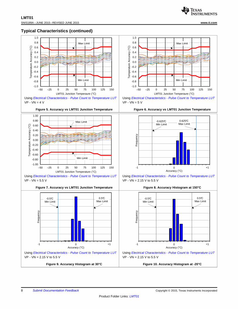
6.9 Typical Characteristics
Using Electrical Characteristics - Pulse Count to Temperature LUT Using Electrical Characteristics - Pulse Count to Temperature LUTVP - VN = 2.15 V VP - VN = 2.4 V
Figure 1. Accuracy vs LMT01 Junction Temperature Figure 2. Accuracy vs LMT01 Junction Temperature
Using Electrical Characteristics - Pulse Count to Temperature LUT Using Electrical Characteristics - Pulse Count to Temperature LUTVP - VN = 2.7 V VP - VN = 3 V
Figure 3. Accuracy vs LMT01 Junction Temperature Figure 4. Accuracy vs LMT01 Junction Temperature
Copyright © 2015, Texas Instruments Incorporated Submit Documentation Feedback 7
Product Folder Links: LMT01
Fre
quen
cy
Accuracy (�C) C024
-1 +1 0
0.5°C Max Limit
-0.5°C Min Limit
Fre
quen
cy
Accuracy (�C) C023
-1 +1 0
0.5°C Max Limit
-0.5°C Min Limit
-1.00
-0.80
-0.60
-0.40
-0.20
0.00
0.20
0.40
0.60
0.80
1.00
±50 ±25 0 25 50 75 100 125 150
Tem
pera
ture
Acc
urac
y (�
C)
LMT01 Junction Temperature (�C) C011
Max Limit
Min Limit
Fre
quen
cy
Accuracy (�C) C025
-1 +1 0
0.625°C Max Limit
-0.625°C Min Limit
-1.0
-0.8
-0.6
-0.4
-0.2
0.0
0.2
0.4
0.6
0.8
1.0
±50 ±25 0 25 50 75 100 125 150
Tem
pera
ture
Acc
urac
y (�
C)
LMT01 Junction Temperaure (�C) C013
Max Limit
Min Limit
-1.0
-0.8
-0.6
-0.4
-0.2
0.0
0.2
0.4
0.6
0.8
1.0
±50 ±25 0 25 50 75 100 125 150
Tem
pera
ture
Acc
urac
y (�
C)
LMT01 Junction Temperaure (�C) C012
Max Limit
Min Limit
LMT01SNIS189A –JUNE 2015–REVISED JUNE 2015 www.ti.com
Typical Characteristics (continued)
Using Electrical Characteristics - Pulse Count to Temperature LUT Using Electrical Characteristics - Pulse Count to Temperature LUTVP - VN = 4 V VP - VN = 5 V
Figure 5. Accuracy vs LMT01 Junction Temperature Figure 6. Accuracy vs LMT01 Junction Temperature
Using Electrical Characteristics - Pulse Count to Temperature LUT Using Electrical Characteristics - Pulse Count to Temperature LUTVP - VN = 5.5 V VP - VN = 2.15 V to 5.5 V
Figure 7. Accuracy vs LMT01 Junction Temperature Figure 8. Accuracy Histogram at 150°C
Using Electrical Characteristics - Pulse Count to Temperature LUT Using Electrical Characteristics - Pulse Count to Temperature LUTVP - VN = 2.15 V to 5.5 V VP - VN = 2.15 V to 5.5 V
Figure 9. Accuracy Histogram at 30°C Figure 10. Accuracy Histogram at -20°C
8 Submit Documentation Feedback Copyright © 2015, Texas Instruments Incorporated
Product Folder Links: LMT01

-1.0
-0.5
0.0
0.5
1.0
1.5
2.0
2.5
3.0
±50 ±25 0 25 50 75 100 125 150
Tem
pera
ture
Acc
urac
y (�
C)
LMT01 Junction Temperaure (�C) C019
0
25
50
75
100
125
150
2 3 4 5 6
Out
put
Cur
rent
(µ
A)
VP - VN (V) C004
Low Level Current
High Level Current
Fre
quen
cy
Accuracy (�C) C020
-1 +1 0
0.6875°C Max Limit
-0.6875°C Min Limit
-1.0
-0.5
0.0
0.5
1.0
1.5
2.0
2.5
3.0
±50 ±25 0 25 50 75 100 125 150
Tem
pera
ture
Acc
urac
y (�
C)
LMT01 Junction Temperaure (�C) C018
Fre
quen
cy
Accuracy (�C) C022
-1 +1 0
0.5625°C Max Limit -0.5625°C
Min Limit
Fre
quen
cy
Accuracy (�C) C021
-1 +1 0
0.5625°C Max Limit -0.5625°C
Min Limit
LMT01www.ti.com SNIS189A –JUNE 2015–REVISED JUNE 2015
Typical Characteristics (continued)
Using LUT Electrical Characteristics - Pulse Count to Temperature Using Electrical Characteristics - Pulse Count to Temperature LUTLUT VP - VN = 2.15 V to 5.5 VVP - VN = 2.15 V to 5.5 V
Figure 11. Accuracy Histogram at -30°C Figure 12. Accuracy Histogram at -40°C
Using LUT Electrical Characteristics - Pulse Count to Temperature Using Temp = (PC/4096 x 256°C ) - 50°CLUT VP - VN = 2.15 VVP - VN = 2.15 V to 5.5 V
Figure 13. Accuracy Histogram at -50°C Figure 14. Accuracy Using Linear Transfer Function
Using Temp = (PC/4096 x 256°C ) - 50°CVP - VN = 5.5V TA = 30°C
Figure 15. Accuracy Using Linear Transfer Function Figure 16. Output Current vs VP-VN Voltage
Copyright © 2015, Texas Instruments Incorporated Submit Documentation Feedback 9
Product Folder Links: LMT01

0
10
20
30
40
50
60
70
80
90
100
110
0 20 40 60 80 100 120 140 160 180 200
Per
cent
of (
Fin
al -
Initi
al)
Val
ue (
%)
Time (seconds) C032
0
10
20
30
40
50
60
70
80
90
100
110
0.0 0.5 1.0 1.5 2.0 2.5 3.0 3.5 4.0 4.5 5.0 5.5 6.0 6.5 7.0
Per
cent
of (
Fin
al -
Initi
al)
Val
ue (
%)
Time (seconds) C031
0
25
50
75
100
125
150
±50 ±25 0 25 50 75 100 125 150
Out
put
Cur
rent
(µ
A)
LMT01 Juntion Temperature (�C) C003
Low Level Current
High Level Current
0
10
20
30
40
50
60
70
80
90
100
110
0 120 240 360 480 600 720 840 960 1080 1200
Per
cent
of (
Fin
al -
Initi
al)
Val
ue (
%)
Time (seconds) C033
LMT01SNIS189A –JUNE 2015–REVISED JUNE 2015 www.ti.com
Typical Characteristics (continued)
VP-VN=3.3 VVP – VN = 3.3 V TINITIAL=23°C, TFINAL=70°C
Figure 17. Output Current vs Temperature Figure 18. Thermal Response in Still Air
VP-VN=3.3 V Air Flow=2.34 VP-VN=3.3 Vmeters/secTINITIAL=23°C, TFINAL=70°C TINITIAL=23°C, TFINAL=70°C
Figure 19. Thermal Response in Moving Air Figure 20. Thermal Response in Stirred Oil
10 Submit Documentation Feedback Copyright © 2015, Texas Instruments Incorporated
Product Folder Links: LMT01
VN
Voltage Regulator
and OutputSignal
Conditioning
VP
LMT01
InterfaceData
ADC
VREF
Thermal DiodeAnalog Circuitry
Chip VDD
Chip VSS
LMT01www.ti.com SNIS189A –JUNE 2015–REVISED JUNE 2015
7 Detailed Description
7.1 OverviewThe LMT01 temperature output is transmitted over a single wire using a train of current pulses that typicallychange from 34 µA to 125 µA. A simple resistor can then be used to convert the current pulses to a voltage. Witha 10 kΩ the output voltage levels range from 340 mV to 1.25 V, typically. A simple microcontroller comparator orexternal transistor can be used convert this signal to valid logic levels the microcontroller can process properlythrough a GPIO pin. The temperature can be determined by gating a simple counter on for a specific timeinterval to count the total number of output pulses. After power is first applied to the device the current level willremain below 34 µA for at most 54ms while the LMT01 is determining the temperature. Once the temperature isdetermined the pulse train will begin. The individual pulse frequency is typically 88 kHz. The LMT01 willcontinuously convert and transmit data when the power is applied approximately every 104 ms (max).
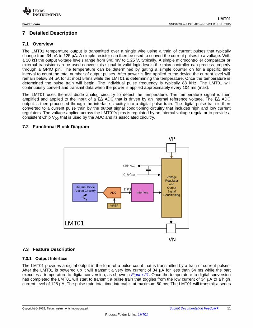
The LMT01 uses thermal diode analog circuitry to detect the temperature. The temperature signal is thenamplified and applied to the input of a ΣΔ ADC that is driven by an internal reference voltage. The ΣΔ ADCoutput is then processed through the interface circuitry into a digital pulse train. The digital pulse train is thenconverted to a current pulse train by the output signal conditioning circuitry that includes high and low currentregulators. The voltage applied across the LMT01's pins is regulated by an internal voltage regulator to provide aconsistent Chip VDD that is used by the ADC and its associated circuitry.
7.2 Functional Block Diagram
7.3 Feature Description
7.3.1 Output InterfaceThe LMT01 provides a digital output in the form of a pulse count that is transmitted by a train of current pulses.After the LMT01 is powered up it will transmit a very low current of 34 µA for less than 54 ms while the partexecutes a temperature to digital conversion, as shown in Figure 21. Once the temperature to digital conversionhas completed the LMT01 will start to transmit a pulse train that toggles from the low current of 34 µA to a highcurrent level of 125 µA. The pulse train total time interval is at maximum 50 ms. The LMT01 will transmit a series
Copyright © 2015, Texas Instruments Incorporated Submit Documentation Feedback 11
Product Folder Links: LMT01

PCTemp 256 C 50 C
4096§ ·
u q � q¨ ¸© ¹
Power
Off
54msmax
Pulse Train
Start of next conversion result data
50ms max
End of data
Power
Start of data transmission
End of data
104ms max
50ms max
Power ON
LMT01SNIS189A –JUNE 2015–REVISED JUNE 2015 www.ti.com
Feature Description (continued)of pulses equivalent to the pulse count at a given temperature as described in Electrical Characteristics - PulseCount to Temperature LUT. After the pulse count has been transmitted the LMT01 current level will remain lowfor the remainder of the 50 ms. The total time for the temperature to digital conversion and the pulse train timeinterval is 104 ms (max). If power is continuously applied the pulse train output will repeat start every 104 ms(max).
Figure 21. Temperature to digital pulse train timing cycle
The LMT01 can be powered down at any time thus conserving system power. Care should be taken though, thata power down wait time of 50ms, minimum, be used before the device is turned on again.
7.3.2 Output Transfer FunctionThe LMT01 will output at minimum 1 pulse and a theoretical maximum 4095 pulses. Each pulse has a weight of0.0625°C. One pulse corresponds to a temperature less than -50°C while a pulse count of 4096 corresponds to atemperature greater than 200°C. Note that the LMT01 is only guaranteed to operate up to 150°C. Exceeding thistemperature by more than 5°C may damage the device. The accuracy of the device degrades as well when150°C in exceeded.
Two different methods of converting the pulse count to a temperature value will be discussed in this section. Thefirst method that will be discussed is the least accurate and uses a first order equation. The second method isthe most accurate and uses linear interpolation of the values found in the look-up table (LUT) as described inElectrical Characteristics - Pulse Count to Temperature LUT.
The output transfer function appears to be linear and can be approximated by the following first order equation:
where• PC is the Pulse Count• Temp is the temperature reading (1)
Table 2 shows some sample calculations using Equation 1
Table 2. Sample Calculations Using Equation 1TEMPERATURE (°C) NUMBER OF PULSES-49.9375 1-49.875 2-20 4800 80030 128050 1600
12 Submit Documentation Feedback Copyright © 2015, Texas Instruments Incorporated
Product Folder Links: LMT01

0
512
1024
1536
2048
2560
3072
3584
4096
±50 ±25 0 25 50 75 100 125 150 175 200 225
Pul
se C
ount
LMT01 Junction Temperature (�C) C002
LMT01www.ti.com SNIS189A –JUNE 2015–REVISED JUNE 2015
Table 2. Sample Calculations Using Equation 1 (continued)TEMPERATURE (°C) NUMBER OF PULSES100 2400150 3200205.9375 4095
The curve shown in Figure 22 shows the output transfer function using equation Equation 1 (blue line) and thelook-up table (LUT) found in Electrical Characteristics - Pulse Count to Temperature LUT (red line). The LMT01output transfer function as described by the LUT appears to be linear, but upon close inspection it can be seenthat it truly is not linear. To actually see the difference, the accuracy obtained by the two methods must becompared.
Figure 22. LMT01 Output Transfer Function
For more exact temperature readings the output pulse count can be converted to temperature using linearinterpolation of the values found in Electrical Characteristics - Pulse Count to Temperature LUT and repeatedhere for convenience.
Table 3. Pulse Count to Temperature Look-up TableTEMPERATURE (°C) PULSE COUNT
MINIMUM TYPICAL MAXIMUM-50 15 26 37-40 172 181 190-30 329 338 347-20 486 494 502-10 643 651 6590 800 808 81610 958 966 97420 1117 1125 113330 1276 1284 129240 1435 1443 145150 1594 1602 161060 1754 1762 177070 1915 1923 193180 2076 2084 209290 2237 2245 2253100 2398 2407 2416110 2560 2569 2578120 2721 2731 2741
Copyright © 2015, Texas Instruments Incorporated Submit Documentation Feedback 13
Product Folder Links: LMT01

tHL= R×C× ln l VF-VS
VF-VHLp
34 and 125 µA
C100pF
OUTPUT
POWER
R10k
VS
VF
VHL
tHLLMT01
-1.0
-0.8
-0.6
-0.4
-0.2
0.0
0.2
0.4
0.6
0.8
1.0
±50 ±25 0 25 50 75 100 125 150
Tem
pera
ture
Acc
urac
y (�
C)
LMT01 Junction Temperaure (�C) C017
Max Limit
Min Limit
-1.0
-0.5
0.0
0.5
1.0
1.5
2.0
2.5
3.0
±50 ±25 0 25 50 75 100 125 150
Tem
pera
ture
Acc
urac
y (�
C)
LMT01 Junction Temperaure (�C) C018
LMT01SNIS189A –JUNE 2015–REVISED JUNE 2015 www.ti.com
Table 3. Pulse Count to Temperature Look-up Table (continued)TEMPERATURE (°C) PULSE COUNT
MINIMUM TYPICAL MAXIMUM130 2883 2893 2903140 3047 3057 3067150 3208 3218 3228
The curves in Figure 23 and Figure 24, show the accuracy of typical units when using the Equation 1 and linearinterpolation using Electrical Characteristics - Pulse Count to Temperature LUT, respectively. When compared,the improved performance when using the LUT linear interpolation method can clearly be seen. For a limitedtemperature range of 25°C to 80°C the error shown in Figure 23 is flat and thus the linear equation will providegood results. For a wide temperature range it is recommended that linear interpolation and the LUT be used.
Figure 23. LMT01 Accuracy when using first order Figure 24. LMT01 Accuracy using linear interpolation ofequation Equation 1 - 92 typical units plotted at (VP - VN) LUT found in Electrical Characteristics - Pulse Count to
= 2.15 V Temperature LUT - 92 typical units plotted at (VP - VN) =2.15 V
7.3.3 Current Output Conversion to VoltageThe minimum voltage drop across the LMT01 must be maintained at 2.15 V during the conversion cycle. Afterthe conversion cycle the minimum voltage drop can decrease to 2.0 V. Thus the LMT01 can be used for lowvoltage applications See Application Information section on low voltage operation and other information onpicking the actual resistor value for different applications conditions. The resistor value is dependent on thepower supply level and it's variation and the threshold level requirements of the circuitry it's driving (i.e. MCUGPIO or Comparator).
Stray capacitance can be introduced when connecting the LMT01 through a long wire. This stray capacitance willinfluence the signal rise and fall times. The wire inductance has negligible effect on the AC signal integrity. Asimple RC time constant model as shown in Figure 25 can be used to determine the rise and fall times.
Figure 25. Simple RC Model for Rise and Fall Times
14 Submit Documentation Feedback Copyright © 2015, Texas Instruments Incorporated
Product Folder Links: LMT01

tr= R×C×2.197
LMT01www.ti.com SNIS189A –JUNE 2015–REVISED JUNE 2015
where• RC as shown in Figure 25• VHL is the target high level• the final voltage VF = 125 µA × R• the start voltage VS = 34 µA × R (2)
For the 10% to 90% level rise time (tr), Equation 2 simplifies to:(3)
Care should be taken to ensure under reverse bias conditions that the LMT01 voltage drop does not exceed300mV, as given in the Absolute Maximum Ratings.
7.4 Device Functional ModesThe only functional mode the LMT01 has is that it provides a pulse count output that is directly proportional totemperature.
Copyright © 2015, Texas Instruments Incorporated Submit Documentation Feedback 15
Product Folder Links: LMT01

TSH= HlIOL× tCONV:tCONV+tDATA;×VCONVp+FHF PC
4096×:IOL+IOH;
2G+F:4096-PC;
4096×IOLGI×
tDATA:tCONV+tDATA;G×VDATAI×R�JA
LMT01SNIS189A –JUNE 2015–REVISED JUNE 2015 www.ti.com
8 Application and Implementation
NOTEInformation in the following applications sections is not part of the TI componentspecification, and TI does not warrant its accuracy or completeness. TI’s customers areresponsible for determining suitability of components for their purposes. Customers shouldvalidate and test their design implementation to confirm system functionality.
8.1 Application Information
8.1.1 Mounting, Temperature Conductivity and Self HeatingThe LMT01 can be applied easily in the same way as other integrated-circuit temperature sensors. It can beglued or cemented to a surface to ensure good temperature conductivity. The temperatures of the lands andtraces to the leads of the LMT01 will also affect the temperature reading so they should be a thin as possible.
Alternatively, the LMT01 can be mounted inside a sealed-end metal tube, and can then be dipped into a bath orscrewed into a threaded hole in a tank. As with any IC, the LMT01 and accompanying wiring and circuits must bekept insulated and dry, to avoid excessive leakage and corrosion. Printed-circuit coatings are often used toensure that moisture cannot corrode the leads or circuit traces.
The LMT01's junction temperature is the actual temperature being measured by the device. The thermalresistance junction-to-ambient (RθJA) is the parameter (from
Thermal Information) used to calculate the rise of a device junction temperature (self heating) due to its averagepower dissipation. The average power dissipation of the LMT01 is dependent on the temperature it is transmittingas it effects the output pulse count and the voltage across the device. Equation 4 is used to calculate the selfheating in the LMT01's die temperature (TSH).
where• TSH is the ambient temperature,• IOL and IOH are the output low and high current level respectively,• VCONV is the voltage across the LMT01 during conversion,• VDATA is the voltage across the LMT01 during data transmission,• tCONV is the conversion time,• tDATA is the data transmission time,• PC is the output pulse count,• RθJA is the junction to ambient package thermal resistance (4)
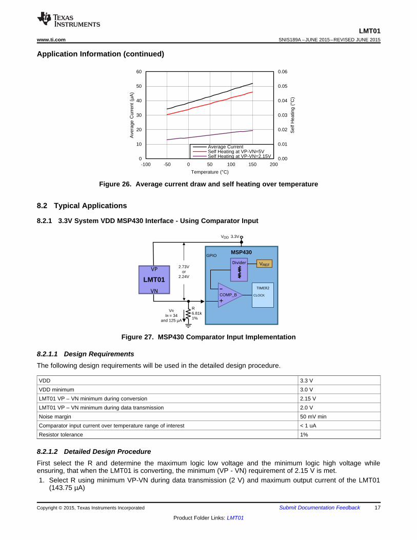
Plotted in the curve Figure 26 are the typical average supply current (black line using left y axis) and the resultingself heating (red and violet lines using right y axis) during continuous conversions. A temperature range of -50°Cto +150°C, a VCONV of 5 V (red line) and 2.15 V (violet line) were used for the self heating calculation. As can beseen in the curve the average power supply current and thus the average self heating changes linearly overtemperature because the number of pulses increases with temperature. A negligible self heating of about 45m°Cis observed at 150°C with continuous conversions. If temperature readings are not required as frequently asevery 100ms, self heating can be minimized by shutting down power to the part periodically thus lowering theaverage power dissipation.
16 Submit Documentation Feedback Copyright © 2015, Texas Instruments Incorporated
Product Folder Links: LMT01
MSP430
VR
IR = 34 and 125 µA
VDD 3.3V
R6.81k1%
GPIO
2.73V or
2.24VLMT01
VP
VN
VREF
+COMP_B
Divider
TIMER2
CLOCK
0.00
0.01
0.02
0.03
0.04
0.05
0.06
0
10
20
30
40
50
60
-100 -50 0 50 100 150 200
Sel
f Hea
ting
(�C
)
Ave
rage
Cur
rent
(µ
A)
Temperature (�C)
Average CurrentSelf Heating at VP-VN=5VSelf Heating at VP-VN=2.15V
C001
LMT01www.ti.com SNIS189A –JUNE 2015–REVISED JUNE 2015
Application Information (continued)
Figure 26. Average current draw and self heating over temperature
8.2 Typical Applications
8.2.1 3.3V System VDD MSP430 Interface - Using Comparator Input
Figure 27. MSP430 Comparator Input Implementation
8.2.1.1 Design RequirementsThe following design requirements will be used in the detailed design procedure.
VDD 3.3 VVDD minimum 3.0 VLMT01 VP – VN minimum during conversion 2.15 VLMT01 VP – VN minimum during data transmission 2.0 VNoise margin 50 mV minComparator input current over temperature range of interest < 1 uAResistor tolerance 1%
8.2.1.2 Detailed Design ProcedureFirst select the R and determine the maximum logic low voltage and the minimum logic high voltage whileensuring, that when the LMT01 is converting, the minimum (VP - VN) requirement of 2.15 V is met.1. Select R using minimum VP-VN during data transmission (2 V) and maximum output current of the LMT01
(143.75 µA)
Copyright © 2015, Texas Instruments Incorporated Submit Documentation Feedback 17
Product Folder Links: LMT01

VCLmin=VREF×:1-V_REF_TOL;×(N-N_TOL)
32-COMP_OFFSET
VCHmax=VREF×:1+V_REF_TOL;×(N+N_TOL)
32+COMP_OFFSET
LMT01SNIS189A –JUNE 2015–REVISED JUNE 2015 www.ti.com
– R = (3.0 V – 2 V) / 143.75 µA = 6.993 k the closest 1% resistor is 6.980 k– 6.993 k is the maximum resistance so if using 1% tolerance resistor the actual resistor value needs to be
1% less than 6.993 k and 6.98 k is 0.2% less than 6.993 k thus 6.81 k should be used.2. Check to see if the LMT01's 2.15 V minimum voltage during conversion requirement is met with maximum
IOL of 39 µA and maximum R of 6.81 k + 1%:– VLMT01 = 3 V - (6.81 k x 1.01) × 39 µA = 2.73 V
3. Find the maximum low level voltage range using maximum R of 6.81k and maximum IOL 39 µA:– VRLmax = (6.81 k x 1.01) × 39 µA = 268 mV
4. Find the minimum high level voltage using the minimum R of 6.81k and minimum IOH of 112.5 uA:– VRHmin = (6.81 k x 0.99) × 112.5 µA = 758 mV
Now select the MSP430 comparator threshold voltage that will enable the LMT01 to communicate to theMSP430 properly.1. The MSP430 voltage will be selected by selecting the internal VREF and then choosing the appropriate 1 of
n/32 settings for n of 1 to 31.– VMID= (VRLmax–VRHmin )/2 + VRHmin = (758 mV - 268 mV)/2 + 268 mV= 513 mV– n = (VMID / VREF ) × 32 = (0.513/2.5) × 32 = 7
2. In order to prevent oscillation of the comparator output hysteresis needs to implemented. The MSP430allows this by enabling different n for rising edge and falling edge of the comparator output. Thus for a fallingcomparator output transition N should be set to 6.
3. Determine the noise margin caused by variation in comparator threshold level. Even though the comparatorthreshold level theoretically is set to VMID, the actual level will vary from device to device due to VREFtolerance, resistor divider tolerance, and comparator offset. For proper operation the COMP_B worst caseinput threshold levels must be within the minimum high and maximum low voltage levels presented across R,VRHmin and VRLmax respectively
where• VREF is the MSP430 COMP_B reference voltage for this example 2.5V,• V_REF_TOL is the tolerance of the VREF of 1% or 0.01,• N is the divisor for the MSP430 or 7• N_TOL is the tolerance of the divisor or 0.5• COMP_OFFSET is the comparator offset specification or 10mV (5)
where• VREF is the MSP430 COMP_B reference voltage for this example 2.5V,• V_REF_TOL is the tolerance of the VREF of 1% or 0.01,• N is the divisor for the MSP430 for the hysteresis setting or 6,• N_TOL is the tolerance of the divisor or 0.5,• COMP_OFFSET is the comparator offset specification or 10mV (6)
The noise margin is the minimum of the two differences:(VRHmin–VCHmax) or (VCHmin–VRLmax) (7)
which works out to be 145 mV.
18 Submit Documentation Feedback Copyright © 2015, Texas Instruments Incorporated
Product Folder Links: LMT01

Time (µs)
VRLmax
VCHmin
VMID
VCHmax
VRHmin
Co
mp
ara
tor
Th
resh
old
an
d V
R
Noise Margin
Noise Margin
GND
VDD
VRHmax
VRLmin
Pulse Count Signal
LMT01www.ti.com SNIS189A –JUNE 2015–REVISED JUNE 2015
Figure 28. Pulse Count Signal Amplitude Variation
8.2.1.3 Setting the MSP430 Threshold and Hysteresis
The comparator hysteresis will determine the noise level that the signal can support without causing thecomparator to trip falsely thus resulting in an inaccurate pulse count. The comparator hysteresis is set by theprecision of the MSP430 and what thresholds it is capable of. For this case as the input signal transitions highthe comparator threshold is dropped by 77 mV thus if the noise on the signal as it transitions is kept below thislevel the comparator will not trip falsely. In addition the MSP430 has a digital filter on the COMP_B output that beused to further filter output transitions that occur too quickly.
8.2.1.4 Application Curves
Amplitude = 200 mV/div Δy at cursors = 500 mV Amplitude = 200 mV/div Δy at cursors = 484 mVTime Base = 10 µs/div Δx at cursors = 11.7 µs Time Base = 10 µs/div Δx at cursors = 11.7 µs
Figure 29. MSP430 COMP_B Input Signal No Capacitance Figure 30. MSP430 COMP_B Input Signal 100pFLoad Capacitance Load
Copyright © 2015, Texas Instruments Incorporated Submit Documentation Feedback 19
Product Folder Links: LMT01

MCU/FPGA/ASIC
34 and 125 µA
VDD 3V to 5.5V
GPIO n
GPIO/COMP
Min 2.0V
Up to 2.0m
GPIO1GPIO2
6.81k (for 3V)
LMT01U1
VP
VN
LMT01U2
VP
VN
LMT01Un
VP
VN
MCU/FPGA/ASIC
34 and 125 µA
3V to 5.5V
7.5k
GPIO
Min 2.0V
ISO734x
ISO
LAT
ION
VCC1
GND1 GND2
VCC2
3V to 5.5V
100k
MMBT3904
VDD
LMT01
VP
VN
MCU/FPGA/ASIC
34 and 125 µA
3.3V
7.5k
GPIO
100k
MMBT3904
VDD
LMT01
VP
VN
LMT01SNIS189A –JUNE 2015–REVISED JUNE 2015 www.ti.com
8.3 System Examples
Figure 31. Transistor Level Shifting
Figure 32. Isolation
Note: to turn off an LMT01 set the GPIO pin connected to VP to high impedance state as setting it low would causethe off LMT01 to be reverse biased.
Figure 33. Connecting Multiple Devices to One MCU Input Pin
20 Submit Documentation Feedback Copyright © 2015, Texas Instruments Incorporated
Product Folder Links: LMT01

VN
VP
LMT01www.ti.com SNIS189A –JUNE 2015–REVISED JUNE 2015
9 Power Supply RecommendationsSince the LMT01 is only a 2-pin device the power pins are common with the signal pins, thus the LMT01 has afloating supply that can vary greatly. The LMT01 has an internal regulator that provides a stable voltage tointernal circuitry.
Care should be taken to prevent reverse biasing of the LMT01 as exceeding the absolute maximum ratings maycause damage to the device.
Power supply ramp rate can effect the accuracy of the first result transmitted by the LMT01. As shown inFigure 34 with a 1ms rise time the LMT01 output code is at 1286 which converts to 30.125°C. The scope photoshown in Figure 35 reflects what happens when the rise time is too slow. As can be seen the power supply(yellow trace) is still ramping up to final value while the LMT01 (red trace) has already started a conversion. Thiscauses the output pulse count to decrease from the 1286, shown previously, to 1282 or 29.875°C. Thus, for slowramp rates it is recommended that the first conversion be discarded. For even slower ramp rates more than oneconversion may have to be discarded as it is recommended that either the power supply be within final valuebefore a conversion is used or that ramp rates be faster than 2.5 ms.
Yellow trace = 1 V/div, Red trace = 100 mV/div, Time Base = 20 Yellow trace = 1V/div, Red trace = 100 mV/div, Time base = 20ms/div ms/div
TA= 30°C LMT01 Pulse Count = 1286 TA=30°C LMT01 Pulse Count = 1282VP-VN = 3.3 V Rise Time = 1 ms VP-VN=3.3 V Rise Time = 100 ms
Figure 34. Output pulse count with appropriate power Figure 35. Output pulse count with slow power supply risesupply rise time time
10 Layout
10.1 Layout GuidelinesThe LMT01 can be mounted to a PCB as shown in Figure 36. Care should be taken to make the traces leadingto the LMT01's pads as small as possible in order to minimize their effect on the temperature the LMT01 ismeasuring.
10.2 Layout Example
Figure 36.
Copyright © 2015, Texas Instruments Incorporated Submit Documentation Feedback 21
Product Folder Links: LMT01

LMT01SNIS189A –JUNE 2015–REVISED JUNE 2015 www.ti.com
11 Device and Documentation Support
11.1 Documentation Support
11.2 Community ResourcesThe following links connect to TI community resources. Linked contents are provided "AS IS" by the respectivecontributors. They do not constitute TI specifications and do not necessarily reflect TI's views; see TI's Terms ofUse.
TI E2E™ Online Community TI's Engineer-to-Engineer (E2E) Community. Created to foster collaborationamong engineers. At e2e.ti.com, you can ask questions, share knowledge, explore ideas and helpsolve problems with fellow engineers.
Design Support TI's Design Support Quickly find helpful E2E forums along with design support tools andcontact information for technical support.
11.3 TrademarksE2E is a trademark of Texas Instruments.All other trademarks are the property of their respective owners.
11.4 Electrostatic Discharge CautionThese devices have limited built-in ESD protection. The leads should be shorted together or the device placed in conductive foamduring storage or handling to prevent electrostatic damage to the MOS gates.
11.5 GlossarySLYZ022 — TI Glossary.
This glossary lists and explains terms, acronyms, and definitions.
12 Mechanical, Packaging, and Orderable InformationThe following pages include mechanical, packaging, and orderable information. This information is the mostcurrent data available for the designated devices. This data is subject to change without notice and revision ofthis document. For browser-based versions of this data sheet, refer to the left-hand navigation.
22 Submit Documentation Feedback Copyright © 2015, Texas Instruments Incorporated
Product Folder Links: LMT01

PACKAGE OPTION ADDENDUM
www.ti.com 28-Jun-2015
Addendum-Page 1
PACKAGING INFORMATION
Orderable Device Status(1)
Package Type PackageDrawing
Pins PackageQty
Eco Plan(2)
Lead/Ball Finish(6)
MSL Peak Temp(3)
Op Temp (°C) Device Marking(4/5)
Samples
LMT01LPG ACTIVE TO-92 LPG 2 1000 Green (RoHS& no Sb/Br)
CU SN N / A for Pkg Type -50 to 150 LMT01
LMT01LPGM ACTIVE TO-92 LPG 2 3000 Green (RoHS& no Sb/Br)
CU SN N / A for Pkg Type -50 to 150 LMT01
(1) The marketing status values are defined as follows:ACTIVE: Product device recommended for new designs.LIFEBUY: TI has announced that the device will be discontinued, and a lifetime-buy period is in effect.NRND: Not recommended for new designs. Device is in production to support existing customers, but TI does not recommend using this part in a new design.PREVIEW: Device has been announced but is not in production. Samples may or may not be available.OBSOLETE: TI has discontinued the production of the device.
(2) Eco Plan - The planned eco-friendly classification: Pb-Free (RoHS), Pb-Free (RoHS Exempt), or Green (RoHS & no Sb/Br) - please check http://www.ti.com/productcontent for the latest availabilityinformation and additional product content details.TBD: The Pb-Free/Green conversion plan has not been defined.Pb-Free (RoHS): TI's terms "Lead-Free" or "Pb-Free" mean semiconductor products that are compatible with the current RoHS requirements for all 6 substances, including the requirement thatlead not exceed 0.1% by weight in homogeneous materials. Where designed to be soldered at high temperatures, TI Pb-Free products are suitable for use in specified lead-free processes.Pb-Free (RoHS Exempt): This component has a RoHS exemption for either 1) lead-based flip-chip solder bumps used between the die and package, or 2) lead-based die adhesive used betweenthe die and leadframe. The component is otherwise considered Pb-Free (RoHS compatible) as defined above.Green (RoHS & no Sb/Br): TI defines "Green" to mean Pb-Free (RoHS compatible), and free of Bromine (Br) and Antimony (Sb) based flame retardants (Br or Sb do not exceed 0.1% by weightin homogeneous material)
(3) MSL, Peak Temp. - The Moisture Sensitivity Level rating according to the JEDEC industry standard classifications, and peak solder temperature.
(4) There may be additional marking, which relates to the logo, the lot trace code information, or the environmental category on the device.
(5) Multiple Device Markings will be inside parentheses. Only one Device Marking contained in parentheses and separated by a "~" will appear on a device. If a line is indented then it is a continuationof the previous line and the two combined represent the entire Device Marking for that device.
(6) Lead/Ball Finish - Orderable Devices may have multiple material finish options. Finish options are separated by a vertical ruled line. Lead/Ball Finish values may wrap to two lines if the finishvalue exceeds the maximum column width.
Important Information and Disclaimer:The information provided on this page represents TI's knowledge and belief as of the date that it is provided. TI bases its knowledge and belief on informationprovided by third parties, and makes no representation or warranty as to the accuracy of such information. Efforts are underway to better integrate information from third parties. TI has taken andcontinues to take reasonable steps to provide representative and accurate information but may not have conducted destructive testing or chemical analysis on incoming materials and chemicals.TI and TI suppliers consider certain information to be proprietary, and thus CAS numbers and other limited information may not be available for release.

PACKAGE OPTION ADDENDUM
www.ti.com 28-Jun-2015
Addendum-Page 2
In no event shall TI's liability arising out of such information exceed the total purchase price of the TI part(s) at issue in this document sold by TI to Customer on an annual basis.

www.ti.com
PACKAGE OUTLINE
4.13.9
2X15.515.1
3X 0.480.33
2X 1.27 0.05
3.253.05
3X 0.510.33
3X 0.510.40
2X ( )45°
0.860.66
1.621.42
2.642.44
2.682.28
5.05MAX
6X 0.076 MAX
2.32.0
2 MAX
(0.55)
4221971/A 03/2015
TO-92 - 5.05 mm max heightLPG0002ATO-92
NOTES: 1. All linear dimensions are in millimeters. Any dimensions in parenthesis are for reference only. Dimensioning and tolerancing per ASME Y14.5M.2. This drawing is subject to change without notice.
1 2
1 2
SCALE 1.300

www.ti.com
EXAMPLE BOARD LAYOUT
TYP ALL AROUND
0.05 MAX (1.07)
(1.7)
(1.27)
(2.54)
(R ) TYP0.05 (1.07)
(1.7)
3X ( ) VIA0.75
4221971/A 03/2015
TO-92 - 5.05 mm max heightLPG0002ATO-92
LAND PATTERN EXAMPLENON-SOLDER MASK DEFINED
SCALE:20X
METALTYP
TYPOPENING
SOLDER MASK
1 2

IMPORTANT NOTICE
Texas Instruments Incorporated and its subsidiaries (TI) reserve the right to make corrections, enhancements, improvements and otherchanges to its semiconductor products and services per JESD46, latest issue, and to discontinue any product or service per JESD48, latestissue. Buyers should obtain the latest relevant information before placing orders and should verify that such information is current andcomplete. All semiconductor products (also referred to herein as “components”) are sold subject to TI’s terms and conditions of salesupplied at the time of order acknowledgment.TI warrants performance of its components to the specifications applicable at the time of sale, in accordance with the warranty in TI’s termsand conditions of sale of semiconductor products. Testing and other quality control techniques are used to the extent TI deems necessaryto support this warranty. Except where mandated by applicable law, testing of all parameters of each component is not necessarilyperformed.TI assumes no liability for applications assistance or the design of Buyers’ products. Buyers are responsible for their products andapplications using TI components. To minimize the risks associated with Buyers’ products and applications, Buyers should provideadequate design and operating safeguards.TI does not warrant or represent that any license, either express or implied, is granted under any patent right, copyright, mask work right, orother intellectual property right relating to any combination, machine, or process in which TI components or services are used. Informationpublished by TI regarding third-party products or services does not constitute a license to use such products or services or a warranty orendorsement thereof. Use of such information may require a license from a third party under the patents or other intellectual property of thethird party, or a license from TI under the patents or other intellectual property of TI.Reproduction of significant portions of TI information in TI data books or data sheets is permissible only if reproduction is without alterationand is accompanied by all associated warranties, conditions, limitations, and notices. TI is not responsible or liable for such altereddocumentation. Information of third parties may be subject to additional restrictions.Resale of TI components or services with statements different from or beyond the parameters stated by TI for that component or servicevoids all express and any implied warranties for the associated TI component or service and is an unfair and deceptive business practice.TI is not responsible or liable for any such statements.Buyer acknowledges and agrees that it is solely responsible for compliance with all legal, regulatory and safety-related requirementsconcerning its products, and any use of TI components in its applications, notwithstanding any applications-related information or supportthat may be provided by TI. Buyer represents and agrees that it has all the necessary expertise to create and implement safeguards whichanticipate dangerous consequences of failures, monitor failures and their consequences, lessen the likelihood of failures that might causeharm and take appropriate remedial actions. Buyer will fully indemnify TI and its representatives against any damages arising out of the useof any TI components in safety-critical applications.In some cases, TI components may be promoted specifically to facilitate safety-related applications. With such components, TI’s goal is tohelp enable customers to design and create their own end-product solutions that meet applicable functional safety standards andrequirements. Nonetheless, such components are subject to these terms.No TI components are authorized for use in FDA Class III (or similar life-critical medical equipment) unless authorized officers of the partieshave executed a special agreement specifically governing such use.Only those TI components which TI has specifically designated as military grade or “enhanced plastic” are designed and intended for use inmilitary/aerospace applications or environments. Buyer acknowledges and agrees that any military or aerospace use of TI componentswhich have not been so designated is solely at the Buyer's risk, and that Buyer is solely responsible for compliance with all legal andregulatory requirements in connection with such use.TI has specifically designated certain components as meeting ISO/TS16949 requirements, mainly for automotive use. In any case of use ofnon-designated products, TI will not be responsible for any failure to meet ISO/TS16949.
Products ApplicationsAudio www.ti.com/audio Automotive and Transportation www.ti.com/automotiveAmplifiers amplifier.ti.com Communications and Telecom www.ti.com/communicationsData Converters dataconverter.ti.com Computers and Peripherals www.ti.com/computersDLP® Products www.dlp.com Consumer Electronics www.ti.com/consumer-appsDSP dsp.ti.com Energy and Lighting www.ti.com/energyClocks and Timers www.ti.com/clocks Industrial www.ti.com/industrialInterface interface.ti.com Medical www.ti.com/medicalLogic logic.ti.com Security www.ti.com/securityPower Mgmt power.ti.com Space, Avionics and Defense www.ti.com/space-avionics-defenseMicrocontrollers microcontroller.ti.com Video and Imaging www.ti.com/videoRFID www.ti-rfid.comOMAP Applications Processors www.ti.com/omap TI E2E Community e2e.ti.comWireless Connectivity www.ti.com/wirelessconnectivity
Mailing Address: Texas Instruments, Post Office Box 655303, Dallas, Texas 75265Copyright © 2015, Texas Instruments Incorporated