Embed Size (px)
Citation preview
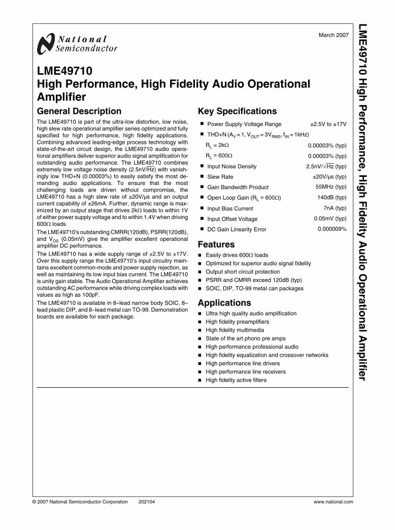
March 2007
LME49710High Performance, High Fidelity Audio OperationalAmplifierGeneral DescriptionThe LME49710 is part of the ultra-low distortion, low noise,high slew rate operational amplifier series optimized and fullyspecified for high performance, high fidelity applications.Combining advanced leading-edge process technology withstate-of-the-art circuit design, the LME49710 audio opera-tional amplifiers deliver superior audio signal amplification foroutstanding audio performance. The LME49710 combinesextremely low voltage noise density (2.5nV/Hz) with vanish-ingly low THD+N (0.00003%) to easily satisfy the most de-manding audio applications. To ensure that the mostchallenging loads are driven without compromise, theLME49710 has a high slew rate of ±20V/μs and an outputcurrent capability of ±26mA. Further, dynamic range is max-imized by an output stage that drives 2kΩ loads to within 1Vof either power supply voltage and to within 1.4V when driving600Ω loads.
The LME49710's outstanding CMRR(120dB), PSRR(120dB),and VOS (0.05mV) give the amplifier excellent operationalamplifier DC performance.
The LME49710 has a wide supply range of ±2.5V to ±17V.Over this supply range the LME49710’s input circuitry main-tains excellent common-mode and power supply rejection, aswell as maintaining its low input bias current. The LME49710is unity gain stable. The Audio Operational Amplifier achievesoutstanding AC performance while driving complex loads withvalues as high as 100pF.
The LME49710 is available in 8–lead narrow body SOIC, 8–lead plastic DIP, and 8–lead metal can TO-99. Demonstrationboards are available for each package.
Key Specifications
Power Supply Voltage Range ±2.5V to ±17V
THD+N (AV = 1, VOUT = 3VRMS, fIN = 1kHz)
RL = 2kΩ 0.00003% (typ)
RL = 600Ω 0.00003% (typ)
Input Noise Density 2.5nV/√Hz (typ)
Slew Rate ±20V/μs (typ)
Gain Bandwidth Product 55MHz (typ)
Open Loop Gain (RL = 600Ω) 140dB (typ)
Input Bias Current 7nA (typ)
Input Offset Voltage 0.05mV (typ)
DC Gain Linearity Error 0.000009%
Features Easily drives 600Ω loads
Optimized for superior audio signal fidelity
Output short circuit protection
PSRR and CMRR exceed 120dB (typ)
SOIC, DIP, TO-99 metal can packages
Applications Ultra high quality audio amplification
High fidelity preamplifiers
High fidelity multimedia
State of the art phono pre amps
High performance professional audio
High fidelity equalization and crossover networks
High performance line drivers
High performance line receivers
High fidelity active filters
© 2007 National Semiconductor Corporation 202104 www.national.com
LM
E49710 H
igh
Perfo
rman
ce, H
igh
Fid
elity
Au
dio
Op
era
tion
al A
mp
lifier
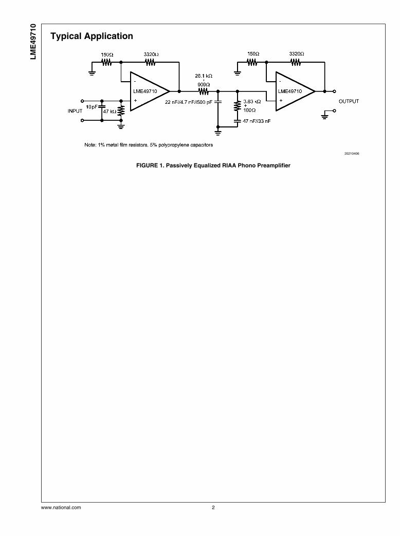
Typical Application
20210406
FIGURE 1. Passively Equalized RIAA Phono Preamplifier
www.national.com 2
LM
E49710
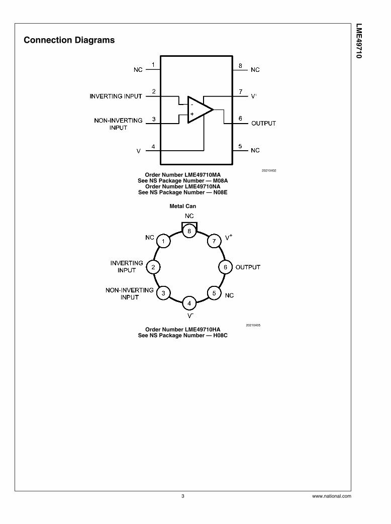
Connection Diagrams
20210402
Order Number LME49710MASee NS Package Number — M08A
Order Number LME49710NASee NS Package Number — N08E
Metal Can
20210405
Order Number LME49710HASee NS Package Number — H08C
3 www.national.com
LM
E49710
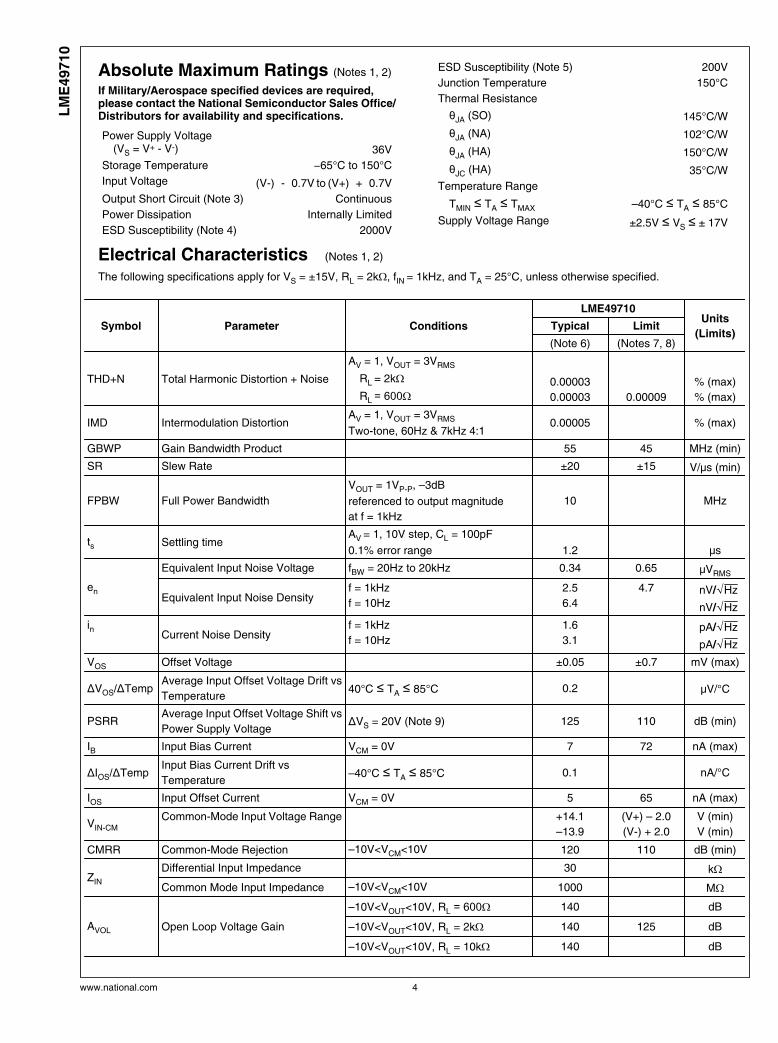
Absolute Maximum Ratings (Notes 1, 2)
If Military/Aerospace specified devices are required,please contact the National Semiconductor Sales Office/Distributors for availability and specifications.
Power Supply Voltage (VS = V+ - V-) 36V
Storage Temperature −65°C to 150°C
Input Voltage (V-) - 0.7V to (V+) + 0.7V
Output Short Circuit (Note 3) Continuous
Power Dissipation Internally Limited
ESD Susceptibility (Note 4) 2000V
ESD Susceptibility (Note 5) 200V
Junction Temperature 150°C
Thermal Resistance
θJA (SO) 145°C/W
θJA (NA) 102°C/W
θJA (HA) 150°C/W
θJC (HA) 35°C/W
Temperature Range
TMIN ≤ TA ≤ TMAX –40°C ≤ TA ≤ 85°C
Supply Voltage Range ±2.5V ≤ VS ≤ ± 17V
Electrical Characteristics (Notes 1, 2)
The following specifications apply for VS = ±15V, RL = 2kΩ, fIN = 1kHz, and TA = 25°C, unless otherwise specified.
Symbol Parameter Conditions
LME49710Units
(Limits)Typical Limit
(Note 6) (Notes 7, 8)
THD+N Total Harmonic Distortion + Noise
AV = 1, VOUT = 3VRMS
RL = 2kΩ RL = 600Ω
0.00003
0.00003 0.00009
% (max)
% (max)
IMD Intermodulation DistortionAV = 1, VOUT = 3VRMS
Two-tone, 60Hz & 7kHz 4:10.00005 % (max)
GBWP Gain Bandwidth Product 55 45 MHz (min)
SR Slew Rate ±20 ±15 V/μs (min)
FPBW Full Power Bandwidth
VOUT = 1VP-P, –3dB
referenced to output magnitude
at f = 1kHz
10
MHz
ts Settling timeAV = 1, 10V step, CL = 100pF
0.1% error range 1.2
μs
en
Equivalent Input Noise Voltage fBW = 20Hz to 20kHz 0.34 0.65 μVRMS
Equivalent Input Noise Densityf = 1kHz
f = 10Hz
2.5
6.4
4.7 nV/√Hz
nV/√Hz
inCurrent Noise Density
f = 1kHz
f = 10Hz
1.6
3.1
pA/√Hz
pA/√Hz
VOS Offset Voltage ±0.05 ±0.7 mV (max)
ΔVOS/ΔTempAverage Input Offset Voltage Drift vs
Temperature40°C ≤ TA ≤ 85°C 0.2
μV/°C
PSRRAverage Input Offset Voltage Shift vs
Power Supply VoltageΔVS = 20V (Note 9) 125 110 dB (min)
IB Input Bias Current VCM = 0V 7 72 nA (max)
ΔIOS/ΔTempInput Bias Current Drift vs
Temperature–40°C ≤ TA ≤ 85°C 0.1
nA/°C
IOS Input Offset Current VCM = 0V 5 65 nA (max)
VIN-CM
Common-Mode Input Voltage Range
+14.1
–13.9
(V+) – 2.0
(V-) + 2.0
V (min)
V (min)
CMRR Common-Mode Rejection –10V<VCM<10V 120 110 dB (min)
ZIN
Differential Input Impedance 30 kΩCommon Mode Input Impedance –10V<VCM<10V 1000 MΩ
AVOL Open Loop Voltage Gain
–10V<VOUT<10V, RL = 600Ω 140 dB
–10V<VOUT<10V, RL = 2kΩ 140 125 dB
–10V<VOUT<10V, RL = 10kΩ 140 dB
www.national.com 4
LM
E49710
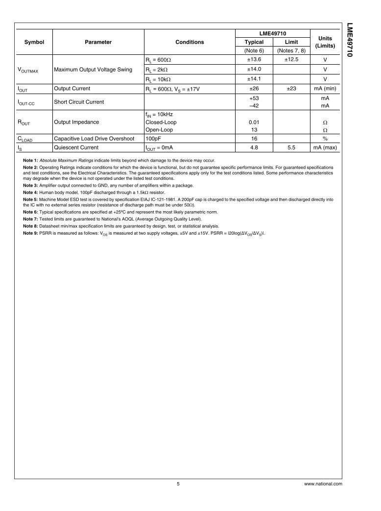
Symbol Parameter Conditions
LME49710Units
(Limits)Typical Limit
(Note 6) (Notes 7, 8)
VOUTMAX Maximum Output Voltage Swing
RL = 600Ω ±13.6 ±12.5 V
RL = 2kΩ ±14.0 V
RL = 10kΩ ±14.1 V
IOUT Output Current RL = 600Ω, VS = ±17V ±26 ±23 mA (min)
IOUT-CC Short Circuit Current +53
–42
mA
mA
ROUT Output Impedance
fIN = 10kHz
Closed-Loop
Open-Loop
0.01
13
ΩΩ
CLOAD Capacitive Load Drive Overshoot 100pF 16 %
IS Quiescent Current IOUT = 0mA 4.8 5.5 mA (max)
Note 1: Absolute Maximum Ratings indicate limits beyond which damage to the device may occur.
Note 2: Operating Ratings indicate conditions for which the device is functional, but do not guarantee specific performance limits. For guaranteed specificationsand test conditions, see the Electrical Characteristics. The guaranteed specifications apply only for the test conditions listed. Some performance characteristicsmay degrade when the device is not operated under the listed test conditions.
Note 3: Amplifier output connected to GND, any number of amplifiers within a package.
Note 4: Human body model, 100pF discharged through a 1.5kΩ resistor.
Note 5: Machine Model ESD test is covered by specification EIAJ IC-121-1981. A 200pF cap is charged to the specified voltage and then discharged directly intothe IC with no external series resistor (resistance of discharge path must be under 50Ω).Note 6: Typical specifications are specified at +25ºC and represent the most likely parametric norm.
Note 7: Tested limits are guaranteed to National's AOQL (Average Outgoing Quality Level).
Note 8: Datasheet min/max specification limits are guaranteed by design, test, or statistical analysis.
Note 9: PSRR is measured as follows: VOS is measured at two supply voltages, ±5V and ±15V. PSRR = |20log(ΔVOS/ΔVS)|.
5 www.national.com
LM
E49710
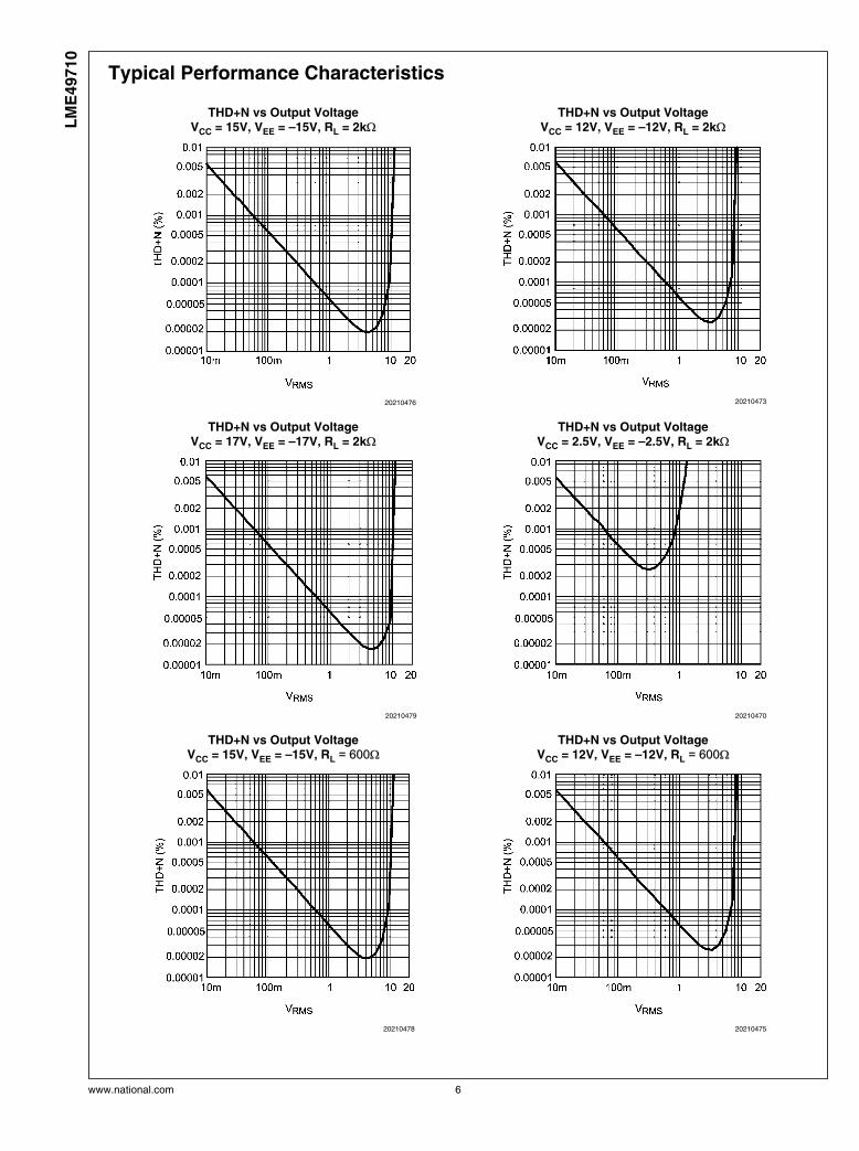
Typical Performance Characteristics
THD+N vs Output VoltageVCC = 15V, VEE = –15V, RL = 2kΩ
20210476
THD+N vs Output VoltageVCC = 12V, VEE = –12V, RL = 2kΩ
20210473
THD+N vs Output VoltageVCC = 17V, VEE = –17V, RL = 2kΩ
20210479
THD+N vs Output VoltageVCC = 2.5V, VEE = –2.5V, RL = 2kΩ
20210470
THD+N vs Output VoltageVCC = 15V, VEE = –15V, RL = 600Ω
20210478
THD+N vs Output VoltageVCC = 12V, VEE = –12V, RL = 600Ω
20210475
www.national.com 6
LM
E49710
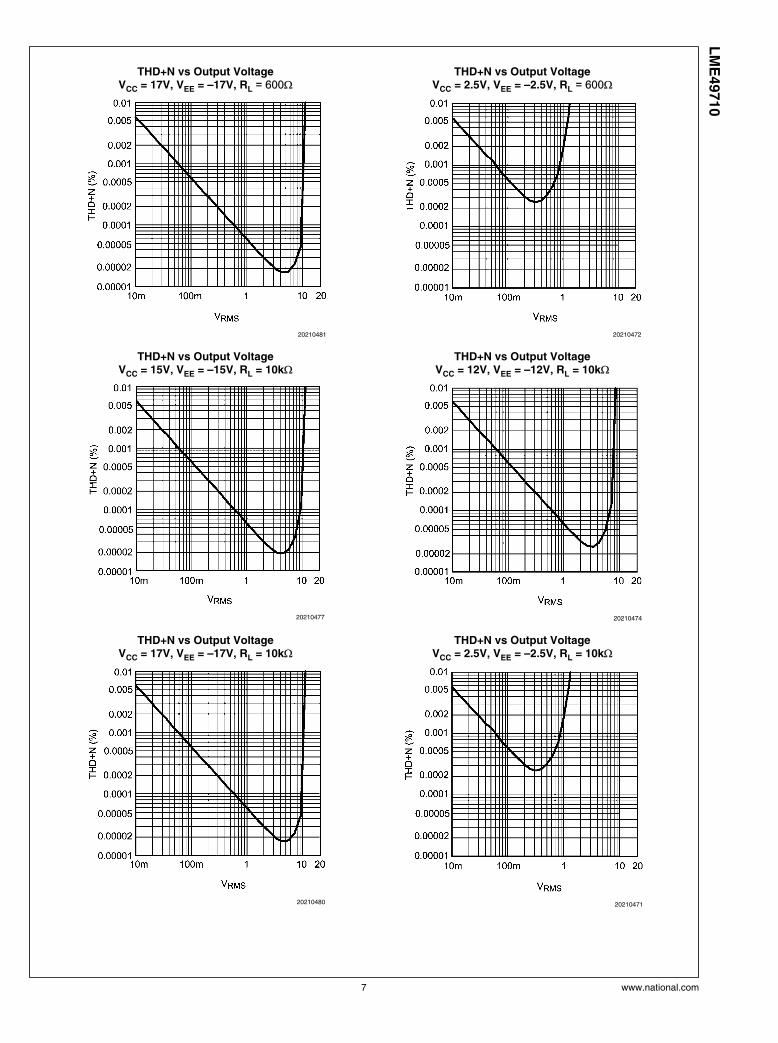
THD+N vs Output VoltageVCC = 17V, VEE = –17V, RL = 600Ω
20210481
THD+N vs Output VoltageVCC = 2.5V, VEE = –2.5V, RL = 600Ω
20210472
THD+N vs Output VoltageVCC = 15V, VEE = –15V, RL = 10kΩ
20210477
THD+N vs Output VoltageVCC = 12V, VEE = –12V, RL = 10kΩ
20210474
THD+N vs Output VoltageVCC = 17V, VEE = –17V, RL = 10kΩ
20210480
THD+N vs Output VoltageVCC = 2.5V, VEE = –2.5V, RL = 10kΩ
20210471
7 www.national.com
LM
E49710
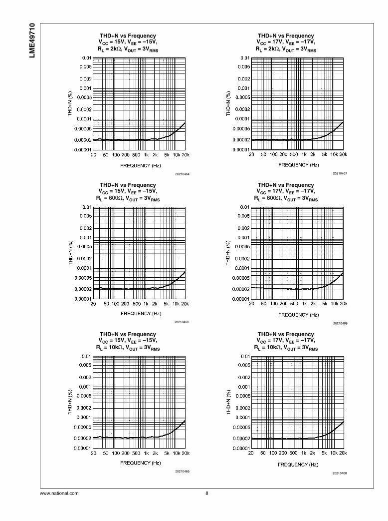
THD+N vs FrequencyVCC = 15V, VEE = –15V,
RL = 2kΩ, VOUT = 3VRMS
20210464
THD+N vs FrequencyVCC = 17V, VEE = –17V,
RL = 2kΩ, VOUT = 3VRMS
20210467
THD+N vs FrequencyVCC = 15V, VEE = –15V,
RL = 600Ω, VOUT = 3VRMS
20210466
THD+N vs FrequencyVCC = 17V, VEE = –17V,
RL = 600Ω, VOUT = 3VRMS
20210469
THD+N vs FrequencyVCC = 15V, VEE = –15V,
RL = 10kΩ, VOUT = 3VRMS
20210465
THD+N vs FrequencyVCC = 17V, VEE = –17V,
RL = 10kΩ, VOUT = 3VRMS
20210468
www.national.com 8
LM
E49710
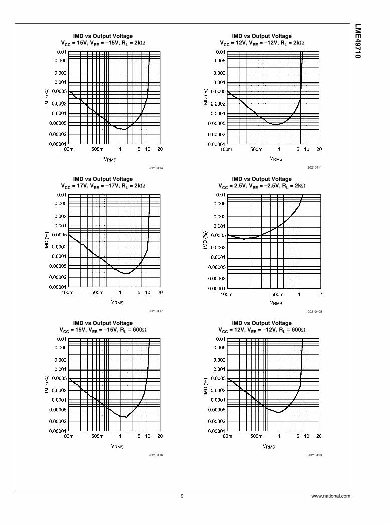
IMD vs Output VoltageVCC = 15V, VEE = –15V, RL = 2kΩ
20210414
IMD vs Output VoltageVCC = 12V, VEE = –12V, RL = 2kΩ
20210411
IMD vs Output VoltageVCC = 17V, VEE = –17V, RL = 2kΩ
20210417
IMD vs Output VoltageVCC = 2.5V, VEE = –2.5V, RL = 2kΩ
20210408
IMD vs Output VoltageVCC = 15V, VEE = –15V, RL = 600Ω
20210416
IMD vs Output VoltageVCC = 12V, VEE = –12V, RL = 600Ω
20210413
9 www.national.com
LM
E49710
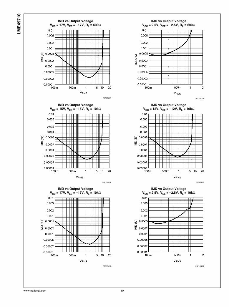
IMD vs Output VoltageVCC = 17V, VEE = –17V, RL = 600Ω
20210419
IMD vs Output VoltageVCC = 2.5V, VEE = –2.5V, RL = 600Ω
20210410
IMD vs Output VoltageVCC = 15V, VEE = –15V, RL = 10kΩ
20210415
IMD vs Output VoltageVCC = 12V, VEE = –12V, RL = 10kΩ
20210412
IMD vs Output VoltageVCC = 17V, VEE = –17V, RL = 10kΩ
20210418
IMD vs Output VoltageVCC = 2.5V, VEE = –2.5V, RL = 10kΩ
20210409
www.national.com 10
LM
E49710
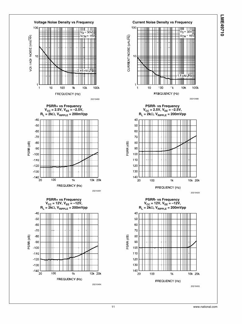
Voltage Noise Density vs Frequency
20210490
Current Noise Density vs Frequency
20210489
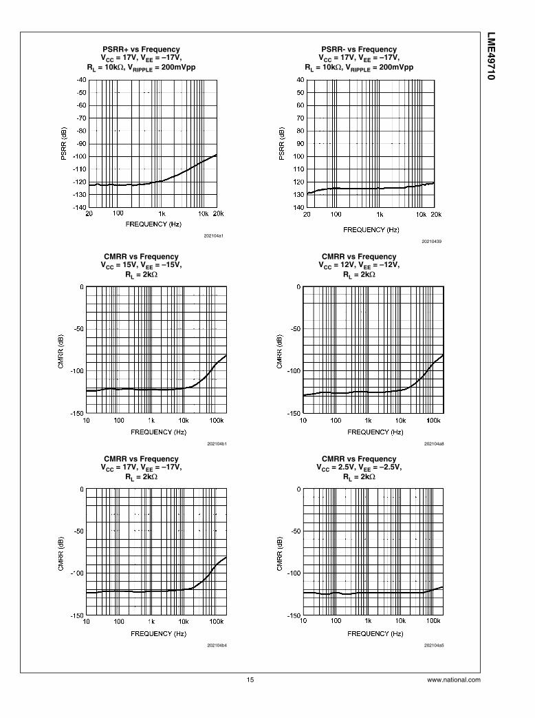
PSRR+ vs FrequencyVCC = 2.5V, VEE = –2.5V,
RL = 2kΩ, VRIPPLE = 200mVpp
20210491
PSRR- vs FrequencyVCC = 2.5V, VEE = –2.5V,
RL = 2kΩ, VRIPPLE = 200mVpp
20210420
PSRR+ vs FrequencyVCC = 12V, VEE = –12V,
RL = 2kΩ, VRIPPLE = 200mVpp
20210494
PSRR- vs FrequencyVCC = 12V, VEE = –12V,
RL = 2kΩ, VRIPPLE = 200mVpp
20210455
11 www.national.com
LM
E49710
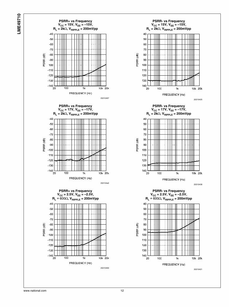
PSRR+ vs FrequencyVCC = 15V, VEE = –15V,
RL = 2kΩ, VRIPPLE = 200mVpp
20210497
PSRR- vs FrequencyVCC = 15V, VEE = –15V,
RL = 2kΩ, VRIPPLE = 200mVpp
20210425
PSRR+ vs FrequencyVCC = 17V, VEE = –17V,
RL = 2kΩ, VRIPPLE = 200mVpp
202104a0
PSRR- vs FrequencyVCC = 17V, VEE = –17V,
RL = 2kΩ, VRIPPLE = 200mVpp
20210438
PSRR+ vs FrequencyVCC = 2.5V, VEE = –2.5V,
RL = 600Ω, VRIPPLE = 200mVpp
20210493
PSRR- vs FrequencyVCC = 2.5V, VEE = –2.5V,
RL = 600Ω, VRIPPLE = 200mVpp
20210421
www.national.com 12
LM
E49710
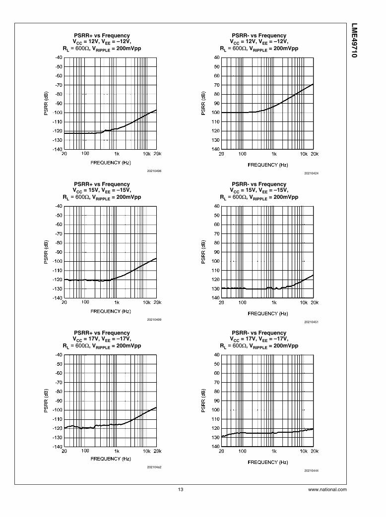
PSRR+ vs FrequencyVCC = 12V, VEE = –12V,
RL = 600Ω, VRIPPLE = 200mVpp
20210496
PSRR- vs FrequencyVCC = 12V, VEE = –12V,
RL = 600Ω, VRIPPLE = 200mVpp
20210424
PSRR+ vs FrequencyVCC = 15V, VEE = –15V,
RL = 600Ω, VRIPPLE = 200mVpp
20210499
PSRR- vs FrequencyVCC = 15V, VEE = –15V,
RL = 600Ω, VRIPPLE = 200mVpp
20210451
PSRR+ vs FrequencyVCC = 17V, VEE = –17V,
RL = 600Ω, VRIPPLE = 200mVpp
202104a2
PSRR- vs FrequencyVCC = 17V, VEE = –17V,
RL = 600Ω, VRIPPLE = 200mVpp
20210444
13 www.national.com
LM
E49710
PSRR+ vs FrequencyVCC = 2.5V, VEE = –2.5V,
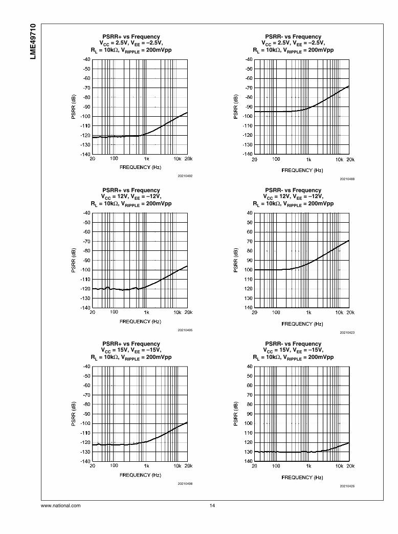
RL = 10kΩ, VRIPPLE = 200mVpp
20210492
PSRR- vs FrequencyVCC = 2.5V, VEE = –2.5V,
RL = 10kΩ, VRIPPLE = 200mVpp
20210488
PSRR+ vs FrequencyVCC = 12V, VEE = –12V,
RL = 10kΩ, VRIPPLE = 200mVpp
20210495
PSRR- vs FrequencyVCC = 12V, VEE = –12V,
RL = 10kΩ, VRIPPLE = 200mVpp
20210423
PSRR+ vs FrequencyVCC = 15V, VEE = –15V,
RL = 10kΩ, VRIPPLE = 200mVpp
20210498
PSRR- vs FrequencyVCC = 15V, VEE = –15V,
RL = 10kΩ, VRIPPLE = 200mVpp
20210426
www.national.com 14
LM
E49710
PSRR+ vs FrequencyVCC = 17V, VEE = –17V,
RL = 10kΩ, VRIPPLE = 200mVpp
202104a1
PSRR- vs FrequencyVCC = 17V, VEE = –17V,
RL = 10kΩ, VRIPPLE = 200mVpp
20210439
CMRR vs FrequencyVCC = 15V, VEE = –15V,
RL = 2kΩ
202104b1
CMRR vs FrequencyVCC = 12V, VEE = –12V,
RL = 2kΩ
202104a8
CMRR vs FrequencyVCC = 17V, VEE = –17V,
RL = 2kΩ
202104b4
CMRR vs FrequencyVCC = 2.5V, VEE = –2.5V,
RL = 2kΩ
202104a5
15 www.national.com
LM
E49710
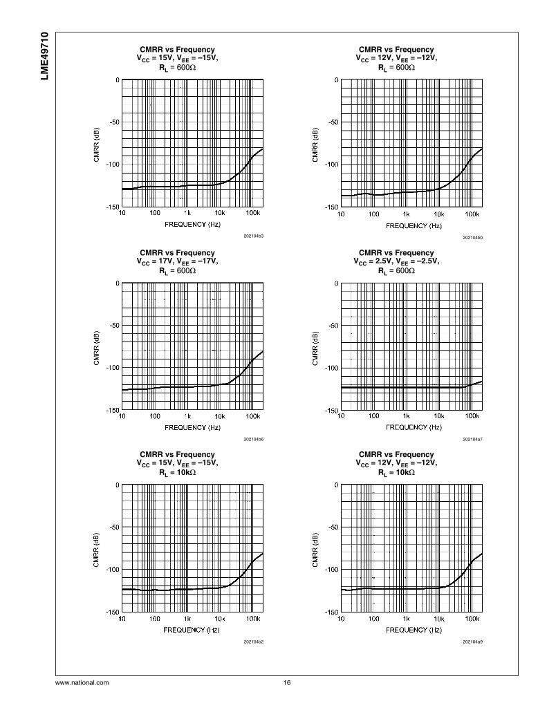
CMRR vs FrequencyVCC = 15V, VEE = –15V,
RL = 600Ω
202104b3
CMRR vs FrequencyVCC = 12V, VEE = –12V,
RL = 600Ω
202104b0
CMRR vs FrequencyVCC = 17V, VEE = –17V,
RL = 600Ω
202104b6
CMRR vs FrequencyVCC = 2.5V, VEE = –2.5V,
RL = 600Ω
202104a7
CMRR vs FrequencyVCC = 15V, VEE = –15V,
RL = 10kΩ
202104b2
CMRR vs FrequencyVCC = 12V, VEE = –12V,
RL = 10kΩ
202104a9
www.national.com 16
LM
E49710
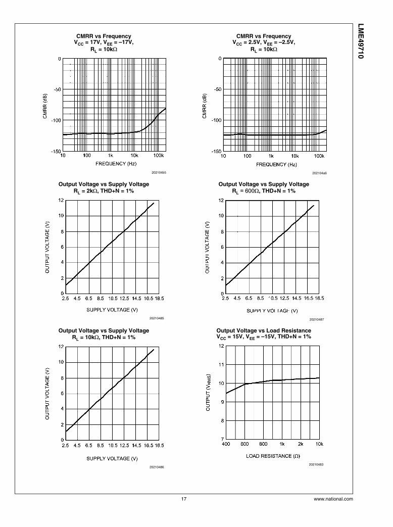
CMRR vs FrequencyVCC = 17V, VEE = –17V,
RL = 10kΩ
202104b5
CMRR vs FrequencyVCC = 2.5V, VEE = –2.5V,
RL = 10kΩ
202104a6
Output Voltage vs Supply VoltageRL = 2kΩ, THD+N = 1%
20210485
Output Voltage vs Supply VoltageRL = 600Ω, THD+N = 1%
20210487
Output Voltage vs Supply VoltageRL = 10kΩ, THD+N = 1%
20210486
Output Voltage vs Load ResistanceVCC = 15V, VEE = –15V, THD+N = 1%
20210483
17 www.national.com
LM
E49710
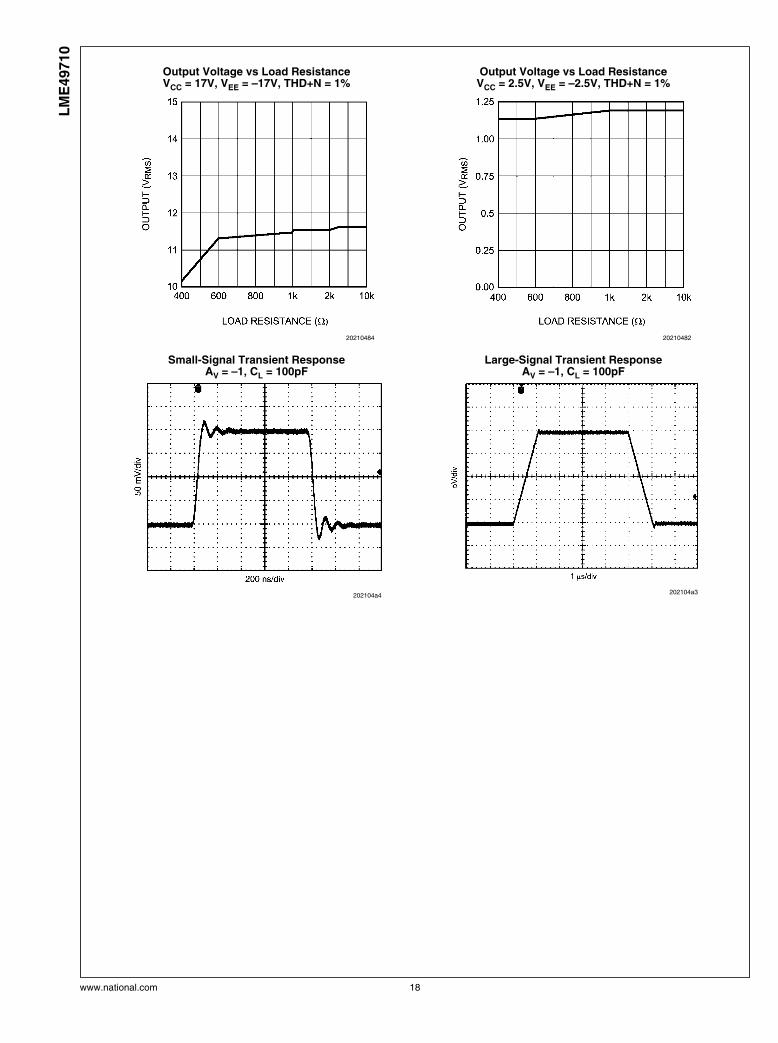
Output Voltage vs Load ResistanceVCC = 17V, VEE = –17V, THD+N = 1%
20210484
Output Voltage vs Load ResistanceVCC = 2.5V, VEE = –2.5V, THD+N = 1%
20210482
Small-Signal Transient ResponseAV = –1, CL = 100pF
202104a4
Large-Signal Transient ResponseAV = –1, CL = 100pF
202104a3
www.national.com 18
LM
E49710
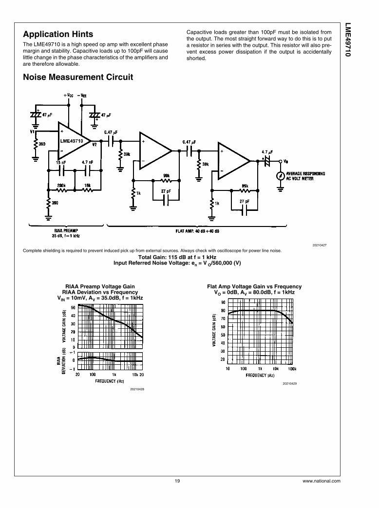
Application HintsThe LME49710 is a high speed op amp with excellent phasemargin and stability. Capacitive loads up to 100pF will causelittle change in the phase characteristics of the amplifiers andare therefore allowable.
Capacitive loads greater than 100pF must be isolated fromthe output. The most straight forward way to do this is to puta resistor in series with the output. This resistor will also pre-vent excess power dissipation if the output is accidentallyshorted.
Noise Measurement Circuit
20210427
Complete shielding is required to prevent induced pick up from external sources. Always check with oscilloscope for power line noise.
Total Gain: 115 dB at f = 1 kHzInput Referred Noise Voltage: en = V O/560,000 (V)
RIAA Preamp Voltage GainRIAA Deviation vs Frequency
VIN = 10mV, AV = 35.0dB, f = 1kHz
20210428
Flat Amp Voltage Gain vs FrequencyVO = 0dB, AV = 80.0dB, f = 1kHz
20210429
19 www.national.com
LM
E49710
Typical Applications
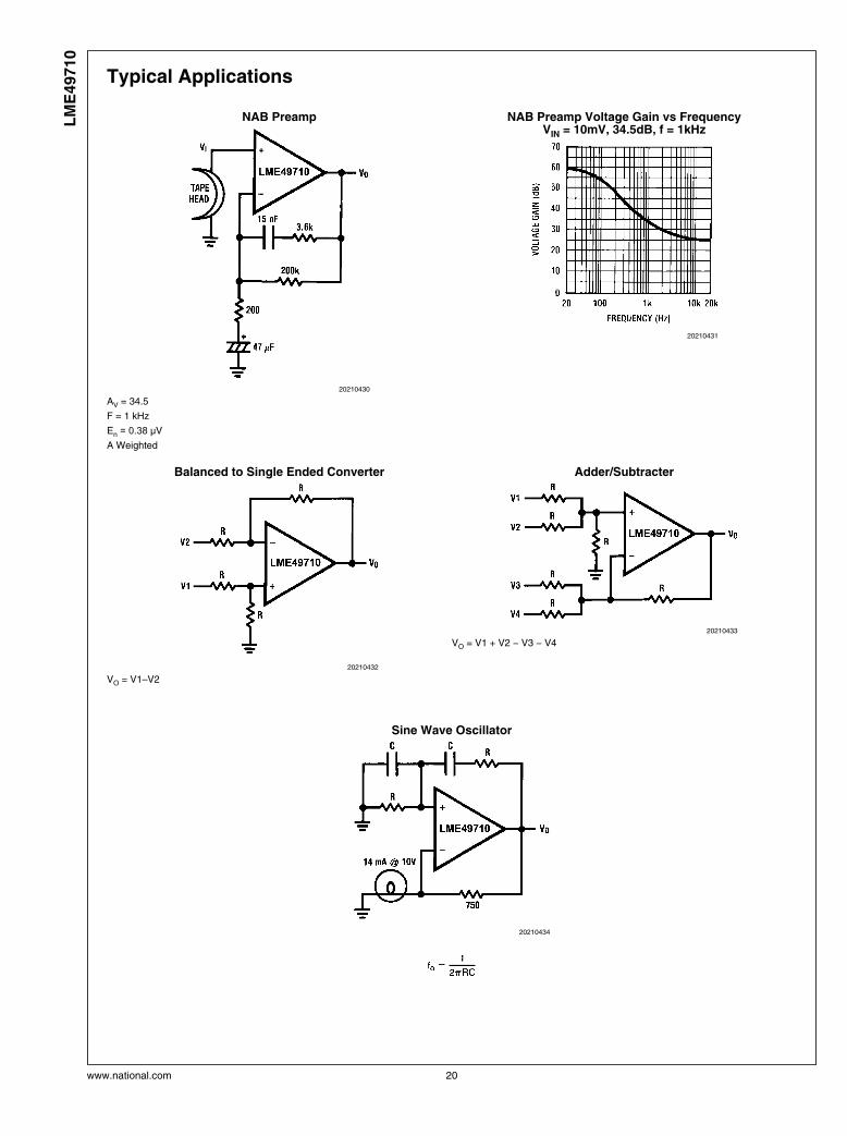
NAB Preamp
20210430
AV = 34.5
F = 1 kHz
En = 0.38 μV
A Weighted
NAB Preamp Voltage Gain vs FrequencyVIN = 10mV, 34.5dB, f = 1kHz
20210431
Balanced to Single Ended Converter
20210432
VO = V1–V2
Adder/Subtracter
20210433
VO = V1 + V2 − V3 − V4
Sine Wave Oscillator
20210434
www.national.com 20
LM
E49710
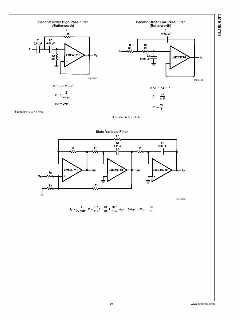
Second Order High Pass Filter(Butterworth)
20210435
Illustration is f0 = 1 kHz
Second Order Low Pass Filter(Butterworth)
20210436
Illustration is f0 = 1 kHz
State Variable Filter
20210437
21 www.national.com
LM
E49710
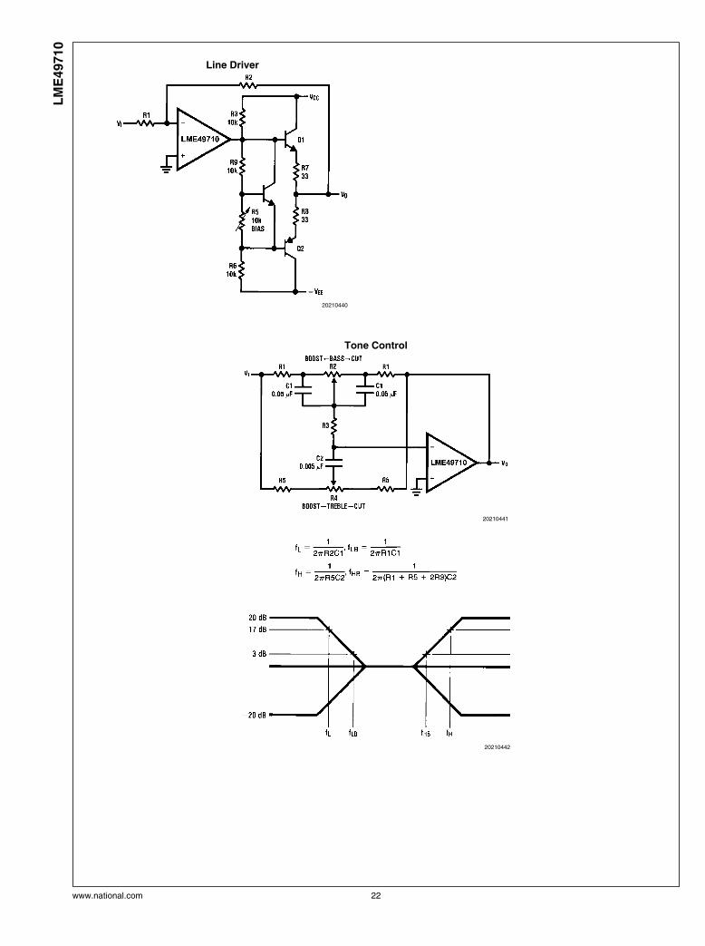
Line Driver
20210440
Tone Control
20210441
20210442
www.national.com 22
LM
E49710
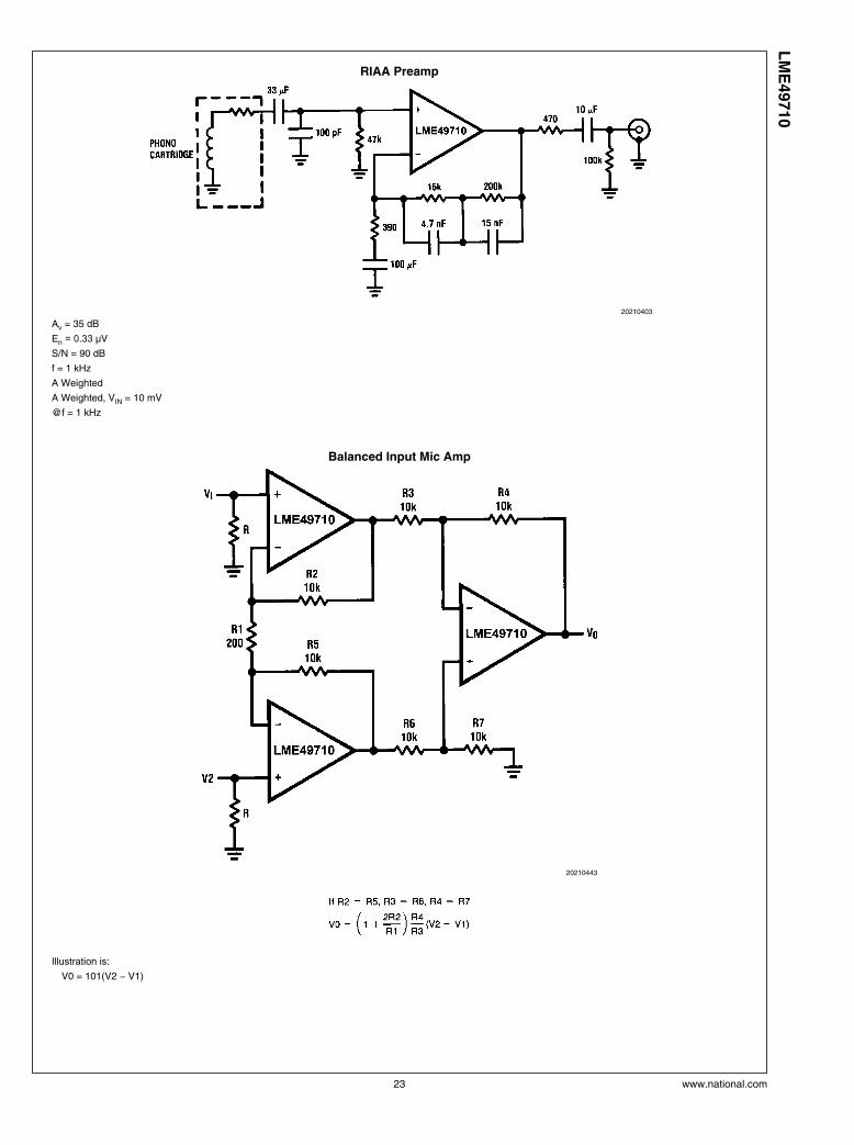
RIAA Preamp
20210403
Av = 35 dB
En = 0.33 μV
S/N = 90 dB
f = 1 kHz
A Weighted
A Weighted, VIN = 10 mV
@f = 1 kHz
Balanced Input Mic Amp
20210443
Illustration is:
V0 = 101(V2 − V1)
23 www.national.com
LM
E49710
Application Information
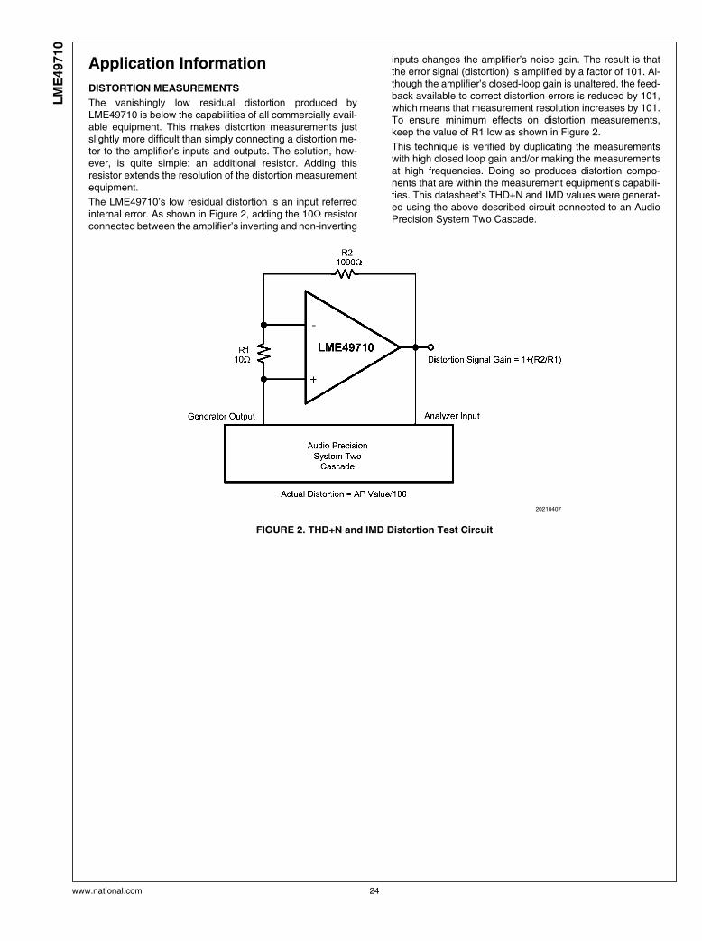
DISTORTION MEASUREMENTS
The vanishingly low residual distortion produced byLME49710 is below the capabilities of all commercially avail-able equipment. This makes distortion measurements justslightly more difficult than simply connecting a distortion me-ter to the amplifier’s inputs and outputs. The solution, how-ever, is quite simple: an additional resistor. Adding thisresistor extends the resolution of the distortion measurementequipment.
The LME49710’s low residual distortion is an input referredinternal error. As shown in Figure 2, adding the 10Ω resistorconnected between the amplifier’s inverting and non-inverting
inputs changes the amplifier’s noise gain. The result is thatthe error signal (distortion) is amplified by a factor of 101. Al-though the amplifier’s closed-loop gain is unaltered, the feed-back available to correct distortion errors is reduced by 101,which means that measurement resolution increases by 101.To ensure minimum effects on distortion measurements,keep the value of R1 low as shown in Figure 2.
This technique is verified by duplicating the measurementswith high closed loop gain and/or making the measurementsat high frequencies. Doing so produces distortion compo-nents that are within the measurement equipment’s capabili-ties. This datasheet’s THD+N and IMD values were generat-ed using the above described circuit connected to an AudioPrecision System Two Cascade.
20210407
FIGURE 2. THD+N and IMD Distortion Test Circuit
www.national.com 24
LM
E49710
Revision History
Rev Date Description
1.0 11/16/07 Initial release.
1.1 12/12/06 Added the Typical Performance
curves.
1.2 01/15/07 Added more curves and input some
text edits.
1.3 03/09/07 Fixed graphics 20210489 and 90.
25 www.national.com
LM
E49710
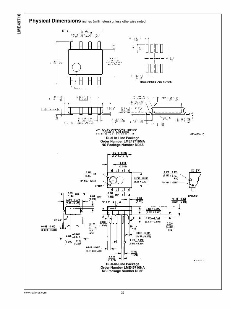
Physical Dimensions inches (millimeters) unless otherwise noted
Dual-In-Line PackageOrder Number LME49710MANS Package Number M08A
Dual-In-Line PackageOrder Number LME49710NANS Package Number N08E
www.national.com 26
LM
E49710
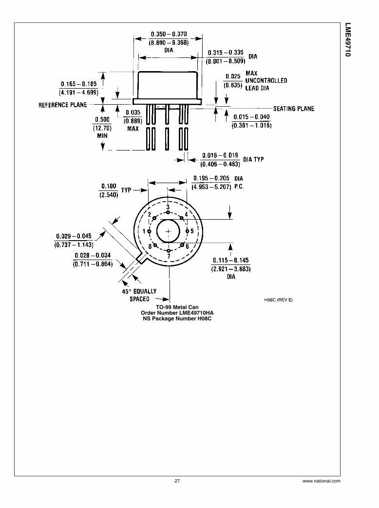
TO-99 Metal CanOrder Number LME49710HANS Package Number H08C
27 www.national.com
LM
E49710
NotesL
ME
49710 H
igh
Perf
orm
an
ce, H
igh
Fid
elity
Au
dio
Op
era
tio
nal A
mp
lifi
er
THE CONTENTS OF THIS DOCUMENT ARE PROVIDED IN CONNECTION WITH NATIONAL SEMICONDUCTOR CORPORATION(“NATIONAL”) PRODUCTS. NATIONAL MAKES NO REPRESENTATIONS OR WARRANTIES WITH RESPECT TO THE ACCURACYOR COMPLETENESS OF THE CONTENTS OF THIS PUBLICATION AND RESERVES THE RIGHT TO MAKE CHANGES TOSPECIFICATIONS AND PRODUCT DESCRIPTIONS AT ANY TIME WITHOUT NOTICE. NO LICENSE, WHETHER EXPRESS,IMPLIED, ARISING BY ESTOPPEL OR OTHERWISE, TO ANY INTELLECTUAL PROPERTY RIGHTS IS GRANTED BY THISDOCUMENT.
TESTING AND OTHER QUALITY CONTROLS ARE USED TO THE EXTENT NATIONAL DEEMS NECESSARY TO SUPPORTNATIONAL’S PRODUCT WARRANTY. EXCEPT WHERE MANDATED BY GOVERNMENT REQUIREMENTS, TESTING OF ALLPARAMETERS OF EACH PRODUCT IS NOT NECESSARILY PERFORMED. NATIONAL ASSUMES NO LIABILITY FORAPPLICATIONS ASSISTANCE OR BUYER PRODUCT DESIGN. BUYERS ARE RESPONSIBLE FOR THEIR PRODUCTS ANDAPPLICATIONS USING NATIONAL COMPONENTS. PRIOR TO USING OR DISTRIBUTING ANY PRODUCTS THAT INCLUDENATIONAL COMPONENTS, BUYERS SHOULD PROVIDE ADEQUATE DESIGN, TESTING AND OPERATING SAFEGUARDS.
EXCEPT AS PROVIDED IN NATIONAL’S TERMS AND CONDITIONS OF SALE FOR SUCH PRODUCTS, NATIONAL ASSUMES NOLIABILITY WHATSOEVER, AND NATIONAL DISCLAIMS ANY EXPRESS OR IMPLIED WARRANTY RELATING TO THE SALEAND/OR USE OF NATIONAL PRODUCTS INCLUDING LIABILITY OR WARRANTIES RELATING TO FITNESS FOR A PARTICULARPURPOSE, MERCHANTABILITY, OR INFRINGEMENT OF ANY PATENT, COPYRIGHT OR OTHER INTELLECTUAL PROPERTYRIGHT.
LIFE SUPPORT POLICY
NATIONAL’S PRODUCTS ARE NOT AUTHORIZED FOR USE AS CRITICAL COMPONENTS IN LIFE SUPPORT DEVICES ORSYSTEMS WITHOUT THE EXPRESS PRIOR WRITTEN APPROVAL OF THE CHIEF EXECUTIVE OFFICER AND GENERALCOUNSEL OF NATIONAL SEMICONDUCTOR CORPORATION. As used herein:
Life support devices or systems are devices which (a) are intended for surgical implant into the body, or (b) support or sustain life andwhose failure to perform when properly used in accordance with instructions for use provided in the labeling can be reasonably expectedto result in a significant injury to the user. A critical component is any component in a life support device or system whose failure to performcan be reasonably expected to cause the failure of the life support device or system or to affect its safety or effectiveness.
National Semiconductor and the National Semiconductor logo are registered trademarks of National Semiconductor Corporation. All otherbrand or product names may be trademarks or registered trademarks of their respective holders.
Copyright© 2007 National Semiconductor Corporation
For the most current product information visit us at www.national.com
National SemiconductorAmericas CustomerSupport CenterEmail:[email protected]: 1-800-272-9959
National Semiconductor EuropeCustomer Support CenterFax: +49 (0) 180-530-85-86Email: [email protected] Tel: +49 (0) 69 9508 6208English Tel: +49 (0) 870 24 0 2171Français Tel: +33 (0) 1 41 91 8790
National Semiconductor AsiaPacific Customer Support CenterEmail: [email protected]
National Semiconductor JapanCustomer Support CenterFax: 81-3-5639-7507Email: [email protected]: 81-3-5639-7560
www.national.com