Embed Size (px)
Citation preview
+
+
+
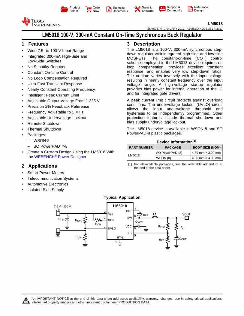
VIN
BST
RON
RTN
SW
VCC
FB
VIN
VOUT
RFB1
R
R
C
UV1
RON
COUT
C
C
BST
IN
RFB2
RUV2
L1
UVLO
+
CVCC
LM50187.5 V - 100 V
1
2
3
4
5
6
8
7
SD
Product
Folder
Order
Now
Technical
Documents
Tools &
Software
Support &Community
ReferenceDesign
An IMPORTANT NOTICE at the end of this data sheet addresses availability, warranty, changes, use in safety-critical applications,intellectual property matters and other important disclaimers. PRODUCTION DATA.
LM5018SNVS787H –JANUARY 2012–REVISED NOVEMBER 2017
LM5018 100-V, 300-mA Constant On-Time Synchronous Buck Regulator
1
1 Features1• Wide 7.5- to 100-V Input Range• Integrated 300-mA High-Side and
Low-Side Switches• No Schottky Required• Constant On-time Control• No Loop Compensation Required• Ultra-Fast Transient Response• Nearly Constant Operating Frequency• Intelligent Peak Current Limit• Adjustable Output Voltage From 1.225 V• Precision 2% Feedback Reference• Frequency Adjustable to 1 MHz• Adjustable Undervoltage Lockout• Remote Shutdown• Thermal Shutdown• Packages:
– WSON-8– SO PowerPAD™-8
• Create a Custom Design Using the LM5018 Withthe WEBENCH® Power Designer
2 Applications• Smart Power Meters• Telecommunication Systems• Automotive Electronics• Isolated Bias Supply
3 DescriptionThe LM5018 is a 100-V, 300-mA synchronous step-down regulator with integrated high-side and low-sideMOSFETs. The constant-on-time (COT) controlscheme employed in the LM5018 device requires noloop compensation, provides excellent transientresponse, and enables very low step-down ratios.The on-time varies inversely with the input voltageresulting in nearly constant frequency over the inputvoltage range. A high-voltage startup regulatorprovides bias power for internal operation of the ICand for integrated gate drivers.
A peak current limit circuit protects against overloadconditions. The undervoltage lockout (UVLO) circuitallows the input undervoltage threshold andhysteresis to be independently programmed. Otherprotection features include thermal shutdown andbias supply undervoltage lockout.
The LM5018 device is available in WSON-8 and SOPowerPAD-8 plastic packages.
Device Information(1)
PART NUMBER PACKAGE BODY SIZE (NOM)
LM5018SO PowerPAD (8) 4.89 mm × 3.90 mmWSON (8) 4.00 mm × 4.00 mm
(1) For all available packages, see the orderable addendum atthe end of the data sheet.
Typical Application
2
LM5018SNVS787H –JANUARY 2012–REVISED NOVEMBER 2017 www.ti.com
Product Folder Links: LM5018
Submit Documentation Feedback Copyright © 2012–2017, Texas Instruments Incorporated
Table of Contents1 Features .................................................................. 12 Applications ........................................................... 13 Description ............................................................. 14 Revision History..................................................... 25 Pin Configuration and Functions ......................... 46 Specifications......................................................... 5
6.1 Absolute Maximum Ratings ..................................... 56.2 ESD Ratings ............................................................ 56.3 Recommended Operating Conditions....................... 56.4 Thermal Information .................................................. 56.5 Electrical Characteristics........................................... 66.6 Timing Requirements ................................................ 66.7 Typical Characteristics .............................................. 7
7 Detailed Description .............................................. 97.1 Overview ................................................................... 97.2 Functional Block Diagram ......................................... 97.3 Feature Description................................................. 10
7.4 Device Functional Modes........................................ 148 Application and Implementation ........................ 15
8.1 Application Information............................................ 158.2 Typical Applications ................................................ 15
9 Power Supply Recommendations ...................... 2410 Layout................................................................... 24
10.1 Layout Guidelines ................................................. 2410.2 Layout Example .................................................... 24
11 Device and Documentation Support ................. 2511.1 Device Support...................................................... 2511.2 Documentation Support ........................................ 2511.3 Receiving Notification of Documentation Updates 2511.4 Community Resources.......................................... 2511.5 Trademarks ........................................................... 2511.6 Electrostatic Discharge Caution............................ 2511.7 Glossary ................................................................ 26
12 Mechanical, Packaging, and OrderableInformation ........................................................... 26
4 Revision History
Changes from Revision G (October 2015) to Revision H Page
• Added WEBENCH links to the data sheet.............................................................................................................................. 1• Deleted lead temperature from the Absolute Maximum Ratings table .................................................................................. 5• Added Receiving Notification of Documentation Updates section ....................................................................................... 25
Changes from Revision F (December 2014) to Revision G Page
• Changed 14 V to 13 V in VCC Regulator section ................................................................................................................. 11• Changed 8 to 4 on equation in Input Capacitor section ....................................................................................................... 17• Changed 0.17 μF to 0.34 μF in Input Capacitor section....................................................................................................... 17
Changes from Revision E (December 2013) to Revision F Page
• Added Pin Configuration and Functions section, ESD Ratings table, Feature Description section, Device FunctionalModes, Application and Implementation section, Power Supply Recommendations section, Layout section, Deviceand Documentation Support section, and Mechanical, Packaging, and Orderable Information section .............................. 1
• Changed input voltage in Typical Application schematic ...................................................................................................... 1• Added package designators to pin out drawings. ................................................................................................................. 4• Changed Thermal Information table. ...................................................................................................................................... 5• Changed Soft-Start Circuit graphic....................................................................................................................................... 14• Changed Frequency Selection, Inductor Selection, Output Capacitor, Input Capacitor, and UVLO Resistors sections. .... 15• Changed Series Ripple Resistor RC section to Type III Ripple Circuit ................................................................................ 17
Changes from Revision D (December 2013) to Revision E Page
• Added Thermal Parameters. .................................................................................................................................................. 5
3
LM5018www.ti.com SNVS787H –JANUARY 2012–REVISED NOVEMBER 2017
Product Folder Links: LM5018
Submit Documentation FeedbackCopyright © 2012–2017, Texas Instruments Incorporated
Changes from Revision C (September 2013) to Revision D Page
• Changed formatting throughout document to be TI compliant ............................................................................................... 1• Changed minimum operating input voltage from 9 V to 7.5 V in Features ........................................................................... 1• Changed minimum operating input voltage from 9 V to 7.5 V in Typical Application ........................................................... 1• Changed minimum operating input voltage from 9 V to 7.5 V in Pin Descriptions ............................................................... 4• Added Maximum Junction Temperature................................................................................................................................. 5
Changes from Revision B (February 2012) to Revision C Page
• Added SW to RTN (100 ns transient) in Absolute Maximum Ratings ................................................................................... 5
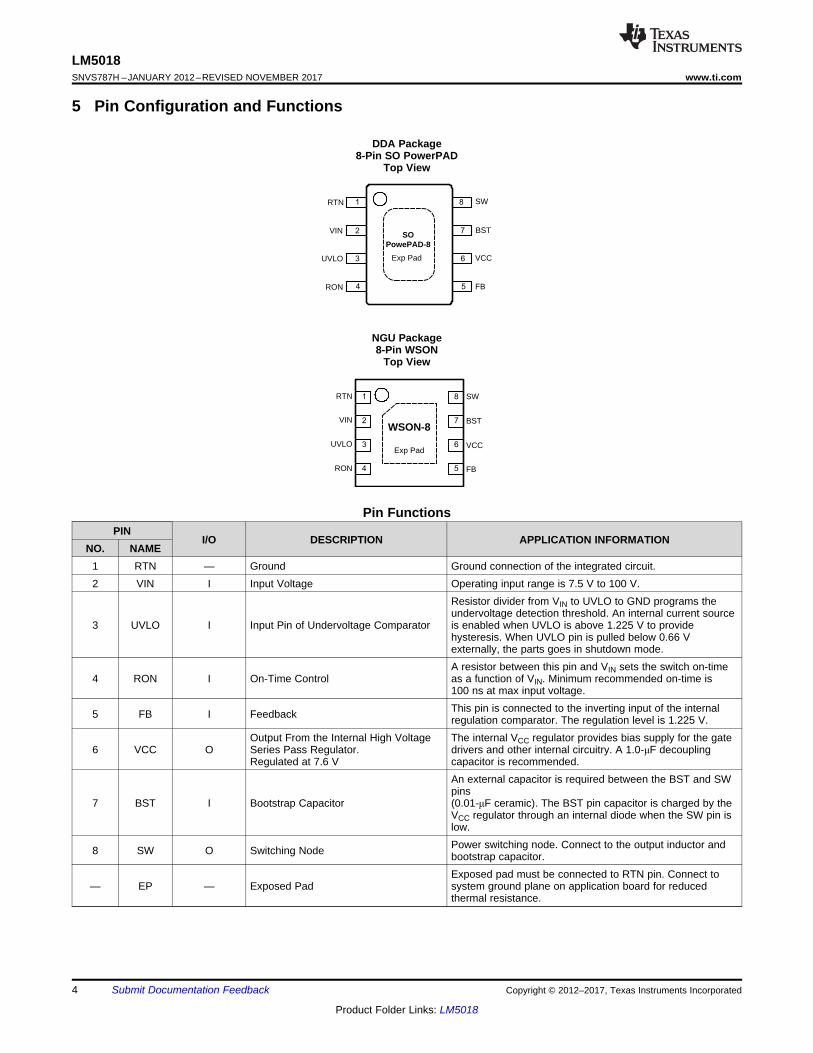
SW
BST
VCC
FB
8
7
6
5
1
2
3
4
UVLO
RON
RTN
VINWSON-8
Exp Pad
UVLO 3
RON 4
RTN 1
VIN 2
8 SW
7 BST
6 VCC
5 FB
SO PowePAD-8
Exp Pad
4
LM5018SNVS787H –JANUARY 2012–REVISED NOVEMBER 2017 www.ti.com
Product Folder Links: LM5018
Submit Documentation Feedback Copyright © 2012–2017, Texas Instruments Incorporated
5 Pin Configuration and Functions
DDA Package8-Pin SO PowerPAD
Top View
NGU Package8-Pin WSON
Top View
Pin FunctionsPIN
I/O DESCRIPTION APPLICATION INFORMATIONNO. NAME
1 RTN — Ground Ground connection of the integrated circuit.2 VIN I Input Voltage Operating input range is 7.5 V to 100 V.
3 UVLO I Input Pin of Undervoltage Comparator
Resistor divider from VIN to UVLO to GND programs theundervoltage detection threshold. An internal current sourceis enabled when UVLO is above 1.225 V to providehysteresis. When UVLO pin is pulled below 0.66 Vexternally, the parts goes in shutdown mode.
4 RON I On-Time ControlA resistor between this pin and VIN sets the switch on-timeas a function of VIN. Minimum recommended on-time is100 ns at max input voltage.
5 FB I Feedback This pin is connected to the inverting input of the internalregulation comparator. The regulation level is 1.225 V.
6 VCC OOutput From the Internal High VoltageSeries Pass Regulator.Regulated at 7.6 V
The internal VCC regulator provides bias supply for the gatedrivers and other internal circuitry. A 1.0-μF decouplingcapacitor is recommended.
7 BST I Bootstrap Capacitor
An external capacitor is required between the BST and SWpins(0.01-μF ceramic). The BST pin capacitor is charged by theVCC regulator through an internal diode when the SW pin islow.
8 SW O Switching Node Power switching node. Connect to the output inductor andbootstrap capacitor.
— EP — Exposed PadExposed pad must be connected to RTN pin. Connect tosystem ground plane on application board for reducedthermal resistance.
5
LM5018www.ti.com SNVS787H –JANUARY 2012–REVISED NOVEMBER 2017
Product Folder Links: LM5018
Submit Documentation FeedbackCopyright © 2012–2017, Texas Instruments Incorporated
(1) Absolute Maximum Ratings are limits beyond which damage to the device may occur. Recommended Operating Conditions areconditions under which operation of the device is intended to be functional. For verified specifications and test conditions, see theElectrical Characteristics. The RTN pin is the GND reference electrically connected to the substrate.
(2) High junction temperatures degrade operating lifetimes. Operating lifetime is de-rated for junction temperatures greater than 125°C
6 Specifications
6.1 Absolute Maximum Ratings (1)
MIN MAX UNITVIN, UVLO to RTN –0.3 100 VSW to RTN –1.5 VIN + 0.3 VSW to RTN (100 ns transient) –5 VIN + 0.3 VBST to VCC 100 VBST to SW 13 VRON to RTN –0.3 100 VVCC to RTN –0.3 13 VFB to RTN –0.3 5 VMaximum junction temperature (2) 150 °CStorage temperature range, Tstg –55 150 °C
(1) JEDEC document JEP155 states that 500-V HBM allows safe manufacturing with a standard ESD control process.(2) JEDEC document JEP157 states that 250-V CDM allows safe manufacturing with a standard ESD control process.
6.2 ESD RatingsVALUE UNIT
V(ESD) Electrostatic dischargeHuman-body model (HBM), per ANSI/ESDA/JEDEC JS-001 (1) ±2000
VCharged-device model (CDM), per JEDEC specification JESD22-C101 (2) ±750
(1) Recommended Operating Conditions are conditions under the device is intended to be functional. For specifications and test conditions,see Electrical Characteristics.
(2) High junction temperatures degrade operating lifetimes. Operating lifetime is de-rated for junction temperatures greater than 125°C.
6.3 Recommended Operating Conditionsover operating free-air temperature range (unless otherwise noted) (1)
MIN MAX UNITVIN voltage 7.5 100 VOperating junction temperature (2) –40 125 °C
(1) For more information about traditional and new thermal metrics, see the IC Package Thermal Metrics application report (SPRA953).
6.4 Thermal Information
THERMAL METRICS (1)
LM5018
UNITNGU (WSON) DDA (SOPowerPAD)
8 PINS 8 PINSRθJA Junction-to-ambient thermal resistance 41.3 41.1 °C/WRθJCbot Junction-to-case (bottom) thermal resistance 3.2 2.4 °C/WΨJB Junction-to-board thermal characteristic parameter 19.2 24.4 °C/WRθJB Junction-to-board thermal resistance 19.1 30.6 °C/WRθJCtop Junction-to-case (top) thermal resistance 34.7 37.3 °C/WΨJT Junction-to-top thermal characteristic parameter 0.3 6.7 °C/W
6
LM5018SNVS787H –JANUARY 2012–REVISED NOVEMBER 2017 www.ti.com
Product Folder Links: LM5018
Submit Documentation Feedback Copyright © 2012–2017, Texas Instruments Incorporated
(1) All hot and cold limits are specified by correlating the electrical characteristics to process and temperature variations and applyingstatistical process control.
(2) VCC provides self bias for the internal gate drive and control circuits. Device thermal limitations limit external loading.
6.5 Electrical CharacteristicsTypical values correspond to TJ = 25°C. Minimum and maximum limits apply over –40°C to 125°C junction temperaturerange, unless otherwise stated. VIN = 48 V unless otherwise stated. See (1) .
PARAMETER TEST CONDITIONS MIN TYP MAX UNITVCC SUPPLYVCC Reg VCC Regulator Output VIN = 48 V, ICC = 20 mA 6.25 7.6 8.55 V
VCC Current Limit VIN = 48 V (2) 26 mAVCC Undervoltage LockoutVoltage (VCC increasing) 4.15 4.5 4.9 V
VCC Undervoltage Hysteresis 300 mVVCC Drop Out Voltage VIN = 9 V, ICC = 20 mA 2.3 VIIN Operating Current Nonswitching, FB = 3 V 1.75 mAIIN Shutdown Current UVLO = 0 V 50 225 µA
SWITCH CHARACTERISTICSBuck Switch RDS(ON) ITEST = 200 mA, BST-SW = 7 V 0.8 1.8 ΩSynchronous RDS(ON) ITEST = 200 mA 0.45 1 ΩGate Drive UVLO VBST − VSW Rising 2.4 3 3.6 VGate Drive UVLO Hysteresis 260 mV
CURRENT LIMITCurrent Limit Threshold 390 575 750 mACurrent Limit Response Time Time to Switch Off 150 nsOFF-Time Generator (Test 1) FB = 0.1 V, VIN = 48 V 12 µsOFF-Time Generator (Test 2) FB = 1.0 V, VIN = 48 V 2.5 µs
REGULATION AND OVERVOLTAGE COMPARATORS
FB Regulation Level Internal Reference Trip Point forSwitch ON 1.2 1.225 1.25 V
FB Overvoltage Threshold Trip Point for Switch OFF 1.62 VFB Bias Current 60 nA
UNDERVOLTAGE SENSING FUNCTIONUV Threshold UV Rising 1.19 1.225 1.26 VUV Hysteresis Input Current UV = 2.5 V –10 –20 –29 µARemote Shutdown Threshold Voltage at UVLO Falling 0.32 0.66 VRemote Shutdown Hysteresis 110 mV
THERMAL SHUTDOWNTsd Thermal Shutdown Temperature 165 °C
Thermal Shutdown Hysteresis 20 °C
6.6 Timing RequirementsTypical values correspond to TJ = 25°C. Minimum and maximum limits apply over –40°C to 125°C junction temperature rangeunless otherwise stated. VIN = 48 V, unless otherwise stated.
MIN NOM MAX UNITON-TIME GENERATOR
TON Test 1 VIN = 32 V, RON = 100 kΩ 270 350 460 nsTON Test 2 VIN = 48 V, RON = 100 kΩ 188 250 336 nsTON Test 3 VIN = 75 V, RON = 250 kΩ 250 370 500 nsTON Test 4 VIN = 10 V, RON = 250 kΩ 1880 3200 4425 ns
MINIMUM OFF-TIMEMinimum Off-Timer FB = 0 V 144 ns
7
LM5018www.ti.com SNVS787H –JANUARY 2012–REVISED NOVEMBER 2017
Product Folder Links: LM5018
Submit Documentation FeedbackCopyright © 2012–2017, Texas Instruments Incorporated
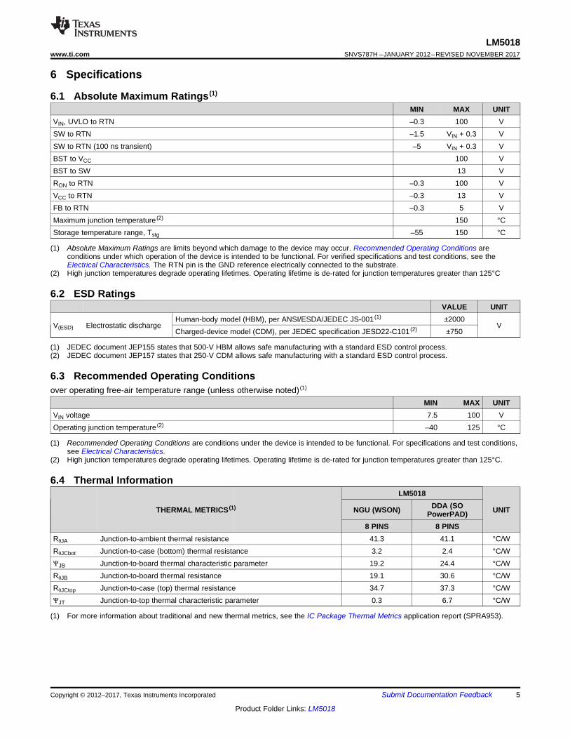
6.7 Typical Characteristics
Figure 1. Efficiency at 240 kHz, 10 V Figure 2. VCC vs VIN
Figure 3. VCC vs ICC Figure 4. ICC vs External VCC
Figure 5. TON vs VIN and RON Figure 6. TOFF (ILIM) vs VFB and VIN
8
LM5018SNVS787H –JANUARY 2012–REVISED NOVEMBER 2017 www.ti.com
Product Folder Links: LM5018
Submit Documentation Feedback Copyright © 2012–2017, Texas Instruments Incorporated
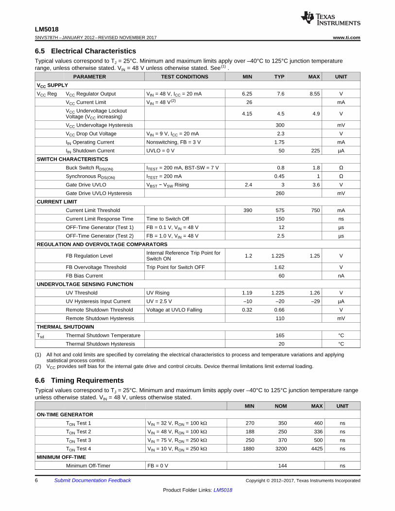
Typical Characteristics (continued)
Figure 7. IIN vs VIN (Operating, Non-Switching) Figure 8. IIN vs VIN (Shutdown)
Figure 9. Switching Frequency vs VIN
FB
VIN VCC
SW
RTN
BST
1.225V
VILIM
LM5018
RON
ILIMCOMPARATOR
+
-
V UVLO
ON/OFF TIMERS
COT CONTROL LOGIC
1.225V
START-UP REGULATOR
VIN
FEEDBACK
DISABLE
THERMALSHUTDOWN
UVLO
OVER-VOLTAGE1.62V
UVLO
4.5V
SD
SHUTDOWN
VDD REG
BG REF
0.66V
20 µA
CURRENT LIMIT
ONE-SHOT
9
LM5018www.ti.com SNVS787H –JANUARY 2012–REVISED NOVEMBER 2017
Product Folder Links: LM5018
Submit Documentation FeedbackCopyright © 2012–2017, Texas Instruments Incorporated
7 Detailed Description
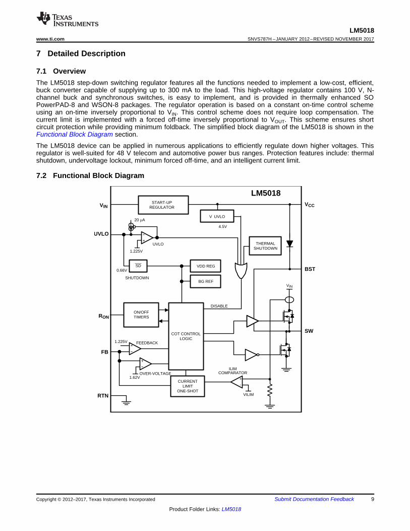
7.1 OverviewThe LM5018 step-down switching regulator features all the functions needed to implement a low-cost, efficient,buck converter capable of supplying up to 300 mA to the load. This high-voltage regulator contains 100 V, N-channel buck and synchronous switches, is easy to implement, and is provided in thermally enhanced SOPowerPAD-8 and WSON-8 packages. The regulator operation is based on a constant on-time control schemeusing an on-time inversely proportional to VIN. This control scheme does not require loop compensation. Thecurrent limit is implemented with a forced off-time inversely proportional to VOUT. This scheme ensures shortcircuit protection while providing minimum foldback. The simplified block diagram of the LM5018 is shown in theFunctional Block Diagram section.
The LM5018 device can be applied in numerous applications to efficiently regulate down higher voltages. Thisregulator is well-suited for 48 V telecom and automotive power bus ranges. Protection features include: thermalshutdown, undervoltage lockout, minimum forced off-time, and an intelligent current limit.
7.2 Functional Block Diagram
FB
SWL1
COUT
RFB2
VOUT
RCLM5018
+RFB1
VOUT (low ripple)
RFB2 + RFB1VOUT = 1.225V xRFB1
VOUTgSW =
K x RON
10
LM5018SNVS787H –JANUARY 2012–REVISED NOVEMBER 2017 www.ti.com
Product Folder Links: LM5018
Submit Documentation Feedback Copyright © 2012–2017, Texas Instruments Incorporated
7.3 Feature Description
7.3.1 Control OverviewThe LM5018 buck regulator employs a control principle based on a comparator and a one-shot on-timer, with theoutput voltage feedback (FB) compared to an internal reference (1.225 V). If the FB voltage is below thereference the internal buck switch is turned on for the one-shot timer period, which is a function of the inputvoltage and the programming resistor (RON). Following the on-time the switch remains off until the FB voltagefalls below the reference, but never before the minimum off-time forced by the minimum off-time one-shot timer.When the FB pin voltage falls below the reference and the minimum off-time one-shot period expires, the buckswitch is turned on for another on-time one-shot period. This will continue until regulation is achieved and the FBvoltage is approximately equal to 1.225 V (typ).
In a synchronous buck converter, the low side (sync) FET is 'on' when the high side (buck) FET is 'off.' Theinductor current ramps up when the high side switch is ‘on’ and ramps down when the high side switch is ‘off’.There is no diode emulation feature in this IC, and therefore, the inductor current may ramp in the negativedirection at light load. This causes the converter to operate in continuous conduction mode (CCM) regardless ofthe output loading. The operating frequency remains relatively constant with load and line variations. Theoperating frequency can be calculated as shown in Equation 1.
where• K = 9 × 10–11 (1)
The output voltage (VOUT) is set by two external resistors (RFB1, RFB2). The regulated output voltage is calculatedas shown in Equation 2.
(2)
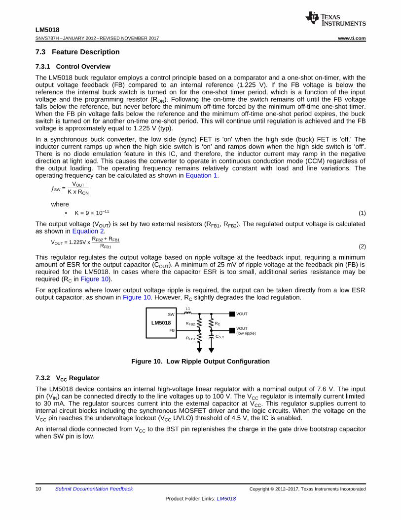
This regulator regulates the output voltage based on ripple voltage at the feedback input, requiring a minimumamount of ESR for the output capacitor (COUT). A minimum of 25 mV of ripple voltage at the feedback pin (FB) isrequired for the LM5018. In cases where the capacitor ESR is too small, additional series resistance may berequired (RC in Figure 10).
For applications where lower output voltage ripple is required, the output can be taken directly from a low ESRoutput capacitor, as shown in Figure 10. However, RC slightly degrades the load regulation.
Figure 10. Low Ripple Output Configuration
7.3.2 VCC RegulatorThe LM5018 device contains an internal high-voltage linear regulator with a nominal output of 7.6 V. The inputpin (VIN) can be connected directly to the line voltages up to 100 V. The VCC regulator is internally current limitedto 30 mA. The regulator sources current into the external capacitor at VCC. This regulator supplies current tointernal circuit blocks including the synchronous MOSFET driver and the logic circuits. When the voltage on theVCC pin reaches the undervoltage lockout (VCC UVLO) threshold of 4.5 V, the IC is enabled.
An internal diode connected from VCC to the BST pin replenishes the charge in the gate drive bootstrap capacitorwhen SW pin is low.
0.07 x VINTOFF(ILIM) = VFB + 0.2V
Ps
10-10 x RONTON =
VIN
11
LM5018www.ti.com SNVS787H –JANUARY 2012–REVISED NOVEMBER 2017
Product Folder Links: LM5018
Submit Documentation FeedbackCopyright © 2012–2017, Texas Instruments Incorporated
Feature Description (continued)At high-input voltages, the power dissipated in the high voltage regulator is significant and can limit the overallachievable output power. As an example, with the input at 48 V and switching at high frequency, the VCCregulator may supply up to 7 mA of current resulting in 48 V × 7 mA = 336 mW of power dissipation. If the VCCvoltage is driven externally by an alternate voltage source between 8.55 V and 13 V, the internal regulator isdisabled. This reduces the power dissipation in the IC.
7.3.3 Regulation ComparatorThe feedback voltage at FB is compared to an internal 1.225 V reference. In normal operation, when the outputvoltage is in regulation, an on-time period is initiated when the voltage at FB falls below 1.225 V. The high sideswitch will stay on for the on-time, causing the FB voltage to rise above 1.225 V. After the on-time period, thehigh side switch will stay off until the FB voltage again falls below 1.225 V. During start-up, the FB voltage will bebelow 1.225 V at the end of each on-time, causing the high side switch to turn on immediately after the minimumforced off-time of 144 ns. The high side switch can be turned off before the on-time is over if the peak current inthe inductor reaches the current limit threshold.
7.3.4 Overvoltage ComparatorThe feedback voltage at FB is compared to an internal 1.62 V reference. If the voltage at FB rises above 1.62 Vthe on-time pulse is immediately terminated. This condition can occur if the input voltage and/or the output loadchanges suddenly. The high-side switch will not turn on again until the voltage at FB falls below 1.225 V.
7.3.5 On-Time GeneratorThe on-time for the LM5018 is determined by the RON resistor and is inversely proportional to the input voltage(VIN), resulting in a nearly constant frequency as VIN is varied over its range. The on-time for the LM5018 can becalculated using Equation 3.
(3)
See Figure 5. RON should be selected for a minimum on-time (at maximum VIN) greater than 100 ns, for properoperation. This requirement limits the maximum switching frequency for high VIN.
7.3.6 Current LimitThe LM5018 device contains an intelligent current limit off-timer. If the current in the buck switch exceeds 575mA, the present cycle is immediately terminated, and a non-resetable off-timer is initiated. The length of off-timeis controlled by the FB voltage and the input voltage VIN. As an example, when FB = 0 V and VIN = 48 V, themaximum off-time is set to 16 μs. This condition occurs when the output is shorted, and during the initial part ofstart-up. This amount of time ensures safe short circuit operation up to the maximum input voltage of 100 V.
In cases of overload where the FB voltage is above zero volts (not a short circuit) the current limit off-time isreduced. Reducing the off-time during less severe overloads reduces the amount of foldback, recovery time, andstart-up time. The off-time is calculated from Equation 4.
(4)
The current limit protection feature is peak limited. The maximum average output will be less than the peak.
7.3.7 N-Channel Buck Switch and DriverThe LM5018 device integrates an N-Channel Buck switch and associated floating high voltage gate driver. Thegate driver circuit works in conjunction with an external bootstrap capacitor and an internal high voltage diode. A0.01-uF ceramic capacitor connected between the BST pin and the SW pin provides the voltage to the driverduring the on-time. During each off-time, the SW pin is at approximately 0 V, and the bootstrap capacitor chargesfrom VCC through the internal diode. The minimum off-timer, set to 144 ns, ensures a minimum time each cycle torecharge the bootstrap capacitor.
+VIN
UVLO
VIN
RUV1
CIN RUV2
2
3
LM5018
12
LM5018SNVS787H –JANUARY 2012–REVISED NOVEMBER 2017 www.ti.com
Product Folder Links: LM5018
Submit Documentation Feedback Copyright © 2012–2017, Texas Instruments Incorporated
Feature Description (continued)7.3.8 Synchronous RectifierThe LM5018 device provides an internal synchronous N-Channel MOSFET rectifier. This MOSFET provides apath for the inductor current to flow when the high-side MOSFET is turned off.
The synchronous rectifier has no diode emulation mode, and is designed to keep the regulator in continuousconduction mode even during light loads which would otherwise result in discontinuous operation.
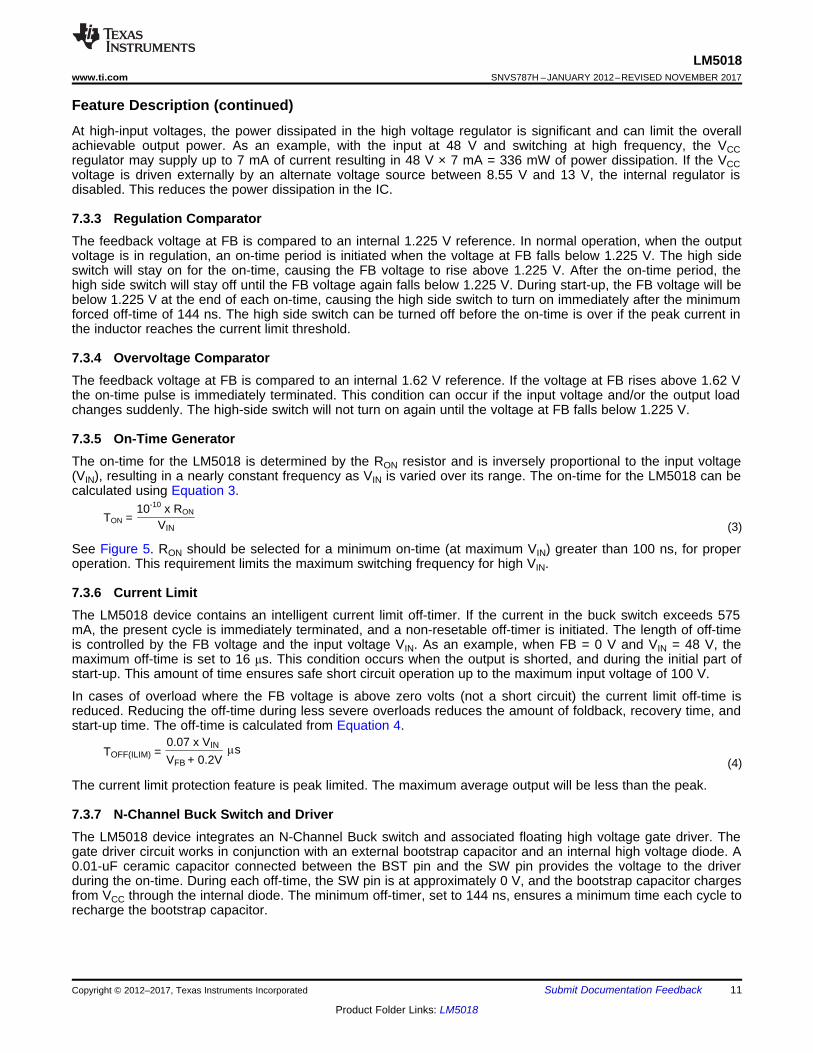
7.3.9 Undervoltage DetectorThe LM5018 device contains a dual level undervoltage lockout (UVLO) circuit. A summary of threshold voltagesand operational states is provided in Device Functional Modes. When the UVLO pin voltage is below 0.66 V, theregulator is in a low current shutdown mode. When the UVLO pin voltage is greater than 0.66 V but less than1.225 V, the regulator is in standby mode. In standby mode the VCC bias regulator is active while the regulatoroutput is disabled. When the VCC pin exceeds the VCC undervoltage threshold and the UVLO pin voltage isgreater than 1.225 V, normal operation begins. An external set-point voltage divider from VIN to GND can beused to set the minimum operating voltage of the regulator.
UVLO hysteresis is accomplished with an internal 20-μA current source that is switched on or off into theimpedance of the set-point divider. When the UVLO threshold is exceeded, the current source is activated toquickly raise the voltage at the UVLO pin. The hysteresis is equal to the value of this current times the resistanceRUV2.
If the UVLO pin is connected directly to the VIN pin, the regulator will begin operation once the VCC undervoltageis satisfied.
Figure 11. UVLO Resistor Setting
7.3.10 Thermal ProtectionThe LM5018 device should be operated so the junction temperature does not exceed 150°C during normaloperation. An internal Thermal Shutdown circuit is provided to protect the LM5018 in the event of a higher thannormal junction temperature. When activated, typically at 165°C, the controller is forced into a low power resetstate, disabling the buck switch and the VCC regulator. This feature prevents catastrophic failures from accidentaldevice overheating. When the junction temperature reduces below 145°C (typical hysteresis = 20°C), the VCCregulator is enabled, and normal operation is resumed.
7.3.11 Ripple ConfigurationLM5018 uses Constant-On-Time (COT) control scheme, in which the on-time is terminated by an on-timer, andthe off-time is terminated by the feedback voltage (VFB) falling below the reference voltage (VREF). Therefore, forstable operation, the feedback voltage must decrease monotonically, in phase with the inductor current duringthe off-time. Furthermore, this change in feedback voltage (VFB) during off-time must be large enough tosuppress any noise component present at the feedback node.
Table 1 shows three different methods for generating appropriate voltage ripple at the feedback node. Type 1and Type 2 ripple circuits couple the ripple at the output of the converter to the feedback node (FB). The outputvoltage ripple has two components:1. Capacitive ripple caused by the inductor current ripple charging/discharging the output capacitor.2. Resistive ripple caused by the inductor current ripple flowing through the ESR of the output capacitor.
RFB1 x RFB2
R2 x (RFB1 + RFB2) + RFB1 x RFB2 VFB = (VCC - VD) x
ûIL(MIN)
25 mVRC
gsw(RFB2||RFB1)
>
5C > Cr = 3300 pF
RrCr <
Cac = 100 nF(VIN(MIN) - VOUT) x TON
25 mV
25 mVRC
ûIL(MIN)
VOUT
VREFx>
GND
To FB
L1
COUT
RFB2
RFB1
VOUT
RC
GND
To FB
L1
COUT
RFB2
RFB1
VOUT
RC
Cac COUT
VOUT
GND
Rr
Cac
Cr
To FB
RFB2
RFB1
L1
13
LM5018www.ti.com SNVS787H –JANUARY 2012–REVISED NOVEMBER 2017
Product Folder Links: LM5018
Submit Documentation FeedbackCopyright © 2012–2017, Texas Instruments Incorporated
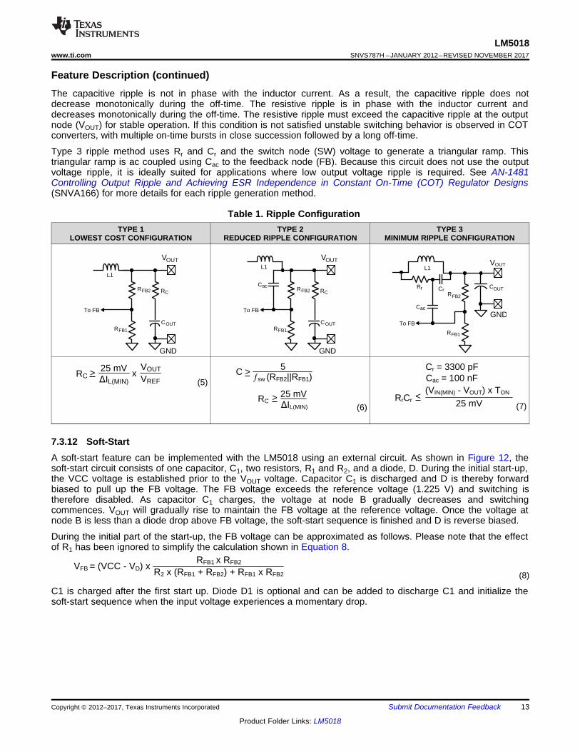
Feature Description (continued)The capacitive ripple is not in phase with the inductor current. As a result, the capacitive ripple does notdecrease monotonically during the off-time. The resistive ripple is in phase with the inductor current anddecreases monotonically during the off-time. The resistive ripple must exceed the capacitive ripple at the outputnode (VOUT) for stable operation. If this condition is not satisfied unstable switching behavior is observed in COTconverters, with multiple on-time bursts in close succession followed by a long off-time.
Type 3 ripple method uses Rr and Cr and the switch node (SW) voltage to generate a triangular ramp. Thistriangular ramp is ac coupled using Cac to the feedback node (FB). Because this circuit does not use the outputvoltage ripple, it is ideally suited for applications where low output voltage ripple is required. See AN-1481Controlling Output Ripple and Achieving ESR Independence in Constant On-Time (COT) Regulator Designs(SNVA166) for more details for each ripple generation method.
Table 1. Ripple ConfigurationTYPE 1
LOWEST COST CONFIGURATIONTYPE 2
REDUCED RIPPLE CONFIGURATIONTYPE 3
MINIMUM RIPPLE CONFIGURATION
(5)
(6) (7)
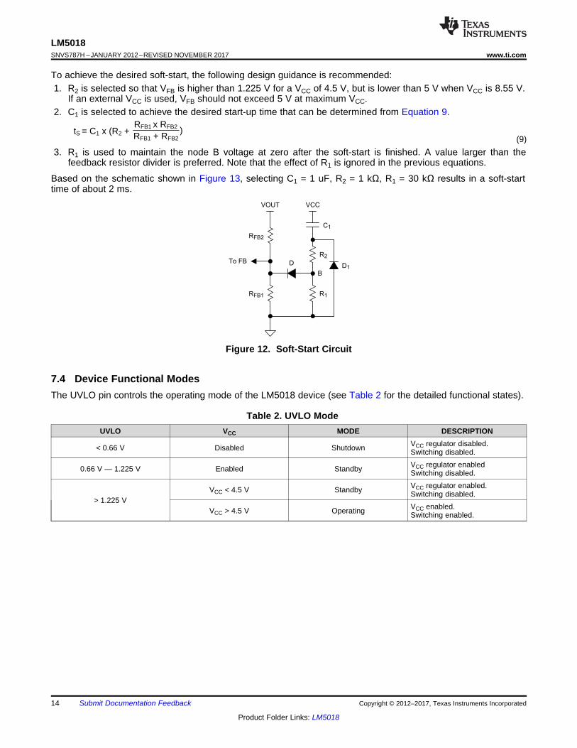
7.3.12 Soft-StartA soft-start feature can be implemented with the LM5018 using an external circuit. As shown in Figure 12, thesoft-start circuit consists of one capacitor, C1, two resistors, R1 and R2, and a diode, D. During the initial start-up,the VCC voltage is established prior to the VOUT voltage. Capacitor C1 is discharged and D is thereby forwardbiased to pull up the FB voltage. The FB voltage exceeds the reference voltage (1.225 V) and switching istherefore disabled. As capacitor C1 charges, the voltage at node B gradually decreases and switchingcommences. VOUT will gradually rise to maintain the FB voltage at the reference voltage. Once the voltage atnode B is less than a diode drop above FB voltage, the soft-start sequence is finished and D is reverse biased.
During the initial part of the start-up, the FB voltage can be approximated as follows. Please note that the effectof R1 has been ignored to simplify the calculation shown in Equation 8.
(8)
C1 is charged after the first start up. Diode D1 is optional and can be added to discharge C1 and initialize thesoft-start sequence when the input voltage experiences a momentary drop.
VOUT
RFB2
VCC
RFB1
To FB D
C
R
R
D
1
2
1
1
B
RFB1 x RFB2
RFB1 + RFB2 tS = C1 x (R2 + )
14
LM5018SNVS787H –JANUARY 2012–REVISED NOVEMBER 2017 www.ti.com
Product Folder Links: LM5018
Submit Documentation Feedback Copyright © 2012–2017, Texas Instruments Incorporated
To achieve the desired soft-start, the following design guidance is recommended:1. R2 is selected so that VFB is higher than 1.225 V for a VCC of 4.5 V, but is lower than 5 V when VCC is 8.55 V.
If an external VCC is used, VFB should not exceed 5 V at maximum VCC.2. C1 is selected to achieve the desired start-up time that can be determined from Equation 9.
(9)3. R1 is used to maintain the node B voltage at zero after the soft-start is finished. A value larger than the
feedback resistor divider is preferred. Note that the effect of R1 is ignored in the previous equations.
Based on the schematic shown in Figure 13, selecting C1 = 1 uF, R2 = 1 kΩ, R1 = 30 kΩ results in a soft-starttime of about 2 ms.
Figure 12. Soft-Start Circuit
7.4 Device Functional ModesThe UVLO pin controls the operating mode of the LM5018 device (see Table 2 for the detailed functional states).
Table 2. UVLO ModeUVLO VCC MODE DESCRIPTION
< 0.66 V Disabled Shutdown VCC regulator disabled.Switching disabled.
0.66 V — 1.225 V Enabled Standby VCC regulator enabledSwitching disabled.
> 1.225 VVCC < 4.5 V Standby VCC regulator enabled.
Switching disabled.
VCC > 4.5 V Operating VCC enabled.Switching enabled.
+
+
+
VINBST
RON
RTN
SW
VCC
FB
VIN
VOUT
R2
R7
R3
C9
C1C4
R1
R5
L1
UVLO
C7
LM5018
12V - 95V
1
2
3
4
5
6
8
7
+C51 F 0.1 F 127 N
14 N
237 N
GND
(TP1)
(TP2)
UVLO/SD
U1 R6
(TP3)
(TP5)
GND
C8
+
D2
EXP1 N
6.98 N
4.7 F
1.5
220 H
0.01 F
1 F
0.1 F
SW
15
LM5018www.ti.com SNVS787H –JANUARY 2012–REVISED NOVEMBER 2017
Product Folder Links: LM5018
Submit Documentation FeedbackCopyright © 2012–2017, Texas Instruments Incorporated
8 Application and Implementation
NOTEInformation in the following applications sections is not part of the TI componentspecification, and TI does not warrant its accuracy or completeness. TI’s customers areresponsible for determining suitability of components for their purposes. Customers shouldvalidate and test their design implementation to confirm system functionality.
8.1 Application InformationThe LM5018 device is step-down DC-DC converter. The device is typically used to convert a higher DC voltageto a lower DC voltage with a maximum available output current of 300 mA. Use the following design procedure toselect component values for the LM5018 device. Alternately, use the WEBENCH® software to generate acomplete design. The WEBENCH software uses an iterative design procedure and accesses a comprehensivedatabase of components when generating a design. This section presents a simplified discussion of the designprocess.
8.2 Typical Applications
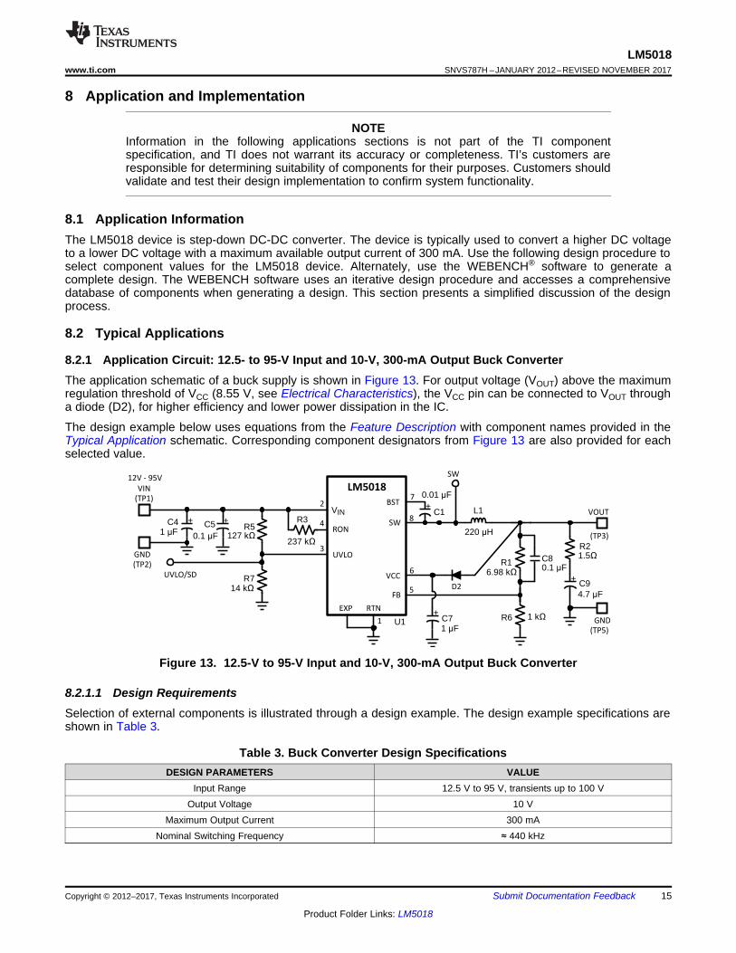
8.2.1 Application Circuit: 12.5- to 95-V Input and 10-V, 300-mA Output Buck ConverterThe application schematic of a buck supply is shown in Figure 13. For output voltage (VOUT) above the maximumregulation threshold of VCC (8.55 V, see Electrical Characteristics), the VCC pin can be connected to VOUT througha diode (D2), for higher efficiency and lower power dissipation in the IC.
The design example below uses equations from the Feature Description with component names provided in theTypical Application schematic. Corresponding component designators from Figure 13 are also provided for eachselected value.
Figure 13. 12.5-V to 95-V Input and 10-V, 300-mA Output Buck Converter
8.2.1.1 Design RequirementsSelection of external components is illustrated through a design example. The design example specifications areshown in Table 3.
Table 3. Buck Converter Design SpecificationsDESIGN PARAMETERS VALUE
Input Range 12.5 V to 95 V, transients up to 100 VOutput Voltage 10 V
Maximum Output Current 300 mANominal Switching Frequency ≈ 440 kHz
LLI OUT
I (max)I (peak) I 346 mA
2
'
VIN - VOUTûIL = L1 x gSW
VOUT
VINx
OUTSW
ON
V¦
K R
u
DMINgSW(MAX) = TON(MIN)
10/48100 ns
= = 2.1 MHz
1 - DMAXgSW(MAX) = TOFF(MIN)
1 - 10/12.5200 ns= = 1 MHz
16
LM5018SNVS787H –JANUARY 2012–REVISED NOVEMBER 2017 www.ti.com
Product Folder Links: LM5018
Submit Documentation Feedback Copyright © 2012–2017, Texas Instruments Incorporated
8.2.1.2 Detailed Design Procedure
8.2.1.2.1 Custom Design With WEBENCH® Tools
Click here to create a custom design using the LM5018 device with the WEBENCH® Power Designer.1. Start by entering the input voltage (VIN), output voltage (VOUT), and output current (IOUT) requirements.2. Optimize the design for key parameters such as efficiency, footprint, and cost using the optimizer dial.3. Compare the generated design with other possible solutions from Texas Instruments.
The WEBENCH Power Designer provides a customized schematic along with a list of materials with real-timepricing and component availability.
In most cases, these actions are available:• Run electrical simulations to see important waveforms and circuit performance• Run thermal simulations to understand board thermal performance• Export customized schematic and layout into popular CAD formats• Print PDF reports for the design, and share the design with colleagues
Get more information about WEBENCH tools at www.ti.com/WEBENCH.
8.2.1.2.2 RFB1, RFB2
VOUT = VFB × (RFB2 / RFB1 + 1), and since VFB = 1.225 V, the ratio of RFB2 to RFB1 is calculated to be 7:1.Standard values are chosen with RFB2 = R1 = 6.98 kΩ and RFB1 = R6 = 1.00 kΩ. Other values could be used aslong as the 7:1 ratio is maintained.
8.2.1.2.3 Frequency Selection
At the minimum input voltage, the maximum switching frequency of LM5018 is restricted by the forced minimumoff-time (TOFF(MIN)) as given by Equation 10.
(10)
Similarly, at maximum input voltage, the maximum switching frequency of LM5018 is restricted by the minimumTON as given by Equation 11.
(11)
Resistor RON sets the nominal switching frequency based on Equation 12.
(12)
Where:K = 9 × 10–11
Operation at high switching frequency results in lower efficiency while providing the smallest solution. For thisexample, 440 kHz was selected, resulting in RON = 253 kΩ. A standard value for RON = R3 = 237 kΩ is selected.
8.2.1.2.4 Inductor Selection
The minimum inductance is selected to limit the inductor ripple current to 20 to 40 percent of the maximum loadcurrent. In addition, the peak inductor current at maximum load must be smaller than the minimum current limitthreshold provided in Electrical Characteristics. The inductor current ripple is given by Equation 13.
(13)
The maximum ripple is observed at maximum input voltage. Substituting VIN = 95 V and ΔIL = 40 percent ×IOUT(max) results in L1 = 169 μH. The higher standard value of 220 μH is chosen. With this value of inductance,peak-to-peak minimum and maximum inductor current ripple of 27 mA and 92 mA occur at the minimum andmaximum input voltages, respectively. The peak inductor and switch current is given by Equation 14.
(14)
VIN(HYS) = IHYS x RUV2
IOUT(MAX)CIN 4 x gSW x ûVIN
>
ûIL(MIN)
25 mVRC
gsw(RFB2||RFB1)
>
5Cac >
ûILCOUT = 8 x gsw x ûVripple
17
LM5018www.ti.com SNVS787H –JANUARY 2012–REVISED NOVEMBER 2017
Product Folder Links: LM5018
Submit Documentation FeedbackCopyright © 2012–2017, Texas Instruments Incorporated
The peak inductor current of 346 mA is smaller than the minimum current limit threshold of 390 mA. The selectedinductor should be able to operate at the maximum current limit of 750 mA during startup and overloadconditions without saturating.
8.2.1.2.5 Output Capacitor
The output capacitor is selected to minimize the capacitive ripple across it. The maximum ripple is observed atmaximum input voltage and is given by Equation 15.
(15)
Where:ΔVripple is the voltage ripple across the capacitor and ΔIL is the peak-to-peak inductor ripple current.
Assuming VIN = 95 V and substituting ΔVripple = 10 mV gives COUT = 2.6 μF. A 4.7-μF standard value is selectedfor COUT = C9. An X5R or X7R type capacitor with a voltage rating 16 V or higher should be selected.
8.2.1.2.6 Type II Ripple Circuit
Type II ripple circuit, as described in Ripple Configuration, is chosen for this example. For a constant on timeconverter to be stable, the injected in-phase ripple should be larger than the capacitive ripple on COUT.
Using type II ripple circuit equations with minimum FB pin ripple of 25 mV, the values of the series resistor RCand ac coupling capacitor Cac can calculated.
(16)
Assuming RFB2 = 6.98 kΩ and RFB1 = 1 kΩ, the calculated minimum value of Cac is 0.013 µF. A standard value of0.1 µF is selected for Cac = C8. The value of the series output resistor RC is calculated for the minimum inputvoltage condition when the inductor ripple current as at a minimum. Using Equation 13 and assuming VIN = 12.5V, the minimum inductor ripple current is 27 mA. The calculated minimum value of RC is 0.93 Ω. A standardvalue of 1.5 Ω is selected for RC = R2 to provide additional ripple for stable switching at low VIN.
8.2.1.2.7 VCC and Bootstrap Capacitor
The VCC capacitor provides charge to bootstrap capacitor as well as internal circuitry and low side gate driver.The bootstrap capacitor provides charge to high-side gate driver. The recommended value for CVCC = C7 = 1 μF.A good value for CBST = C1 = 0.01 μF.
8.2.1.2.8 Input Capacitor
Input capacitor should be large enough to limit the input voltage ripple which can be calculated usingEquation 17.
(17)
Choosing a ΔVIN = 0.5 V gives a minimum CIN = 0.34 μF. A standard value of 1 μF is selected CIN = C4. Theinput capacitor should be rated for the maximum input voltage under all conditions. A 100 V X7R dielectricshould be selected for this design.
Input capacitor should be placed directly across VIN and RTN (pin 2 and 1) of the IC. If it is not possible to placeall of the input capacitor close to the IC, a 0.1-μF capacitor should be placed near the IC to provide a bypasspath for the high frequency component of the switching current.
8.2.1.2.9 UVLO Resistors
The UVLO resistors RUV1 and RUV2 set the UVLO threshold and hysteresis according to the relationship shown inEquation 18 and Equation 19.
where
RUV2VIN (UVLO,rising) = 1.225 V xRUV1
+ 1( )
18
LM5018SNVS787H –JANUARY 2012–REVISED NOVEMBER 2017 www.ti.com
Product Folder Links: LM5018
Submit Documentation Feedback Copyright © 2012–2017, Texas Instruments Incorporated
• IHYS = 20 μA (18)
(19)
Setting UVLO hysteresis of 2.5 V and UVLO rising threshold of 12 V results in RUV1 = 14.53 kΩ andRUV2 = 125 kΩ. Selecting standard values of RUV1 = R7 = 14 kΩ and RUV2 = R5 = 127 kΩ results in UVLOthreshold and hysteresis of 12.4 V and 2.5 V respectively.
8.2.1.3 Application Curves
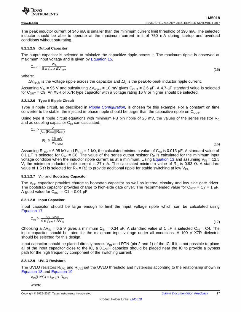
Figure 14. Efficiency vs Load Current Figure 15. Frequency vs Input Voltage
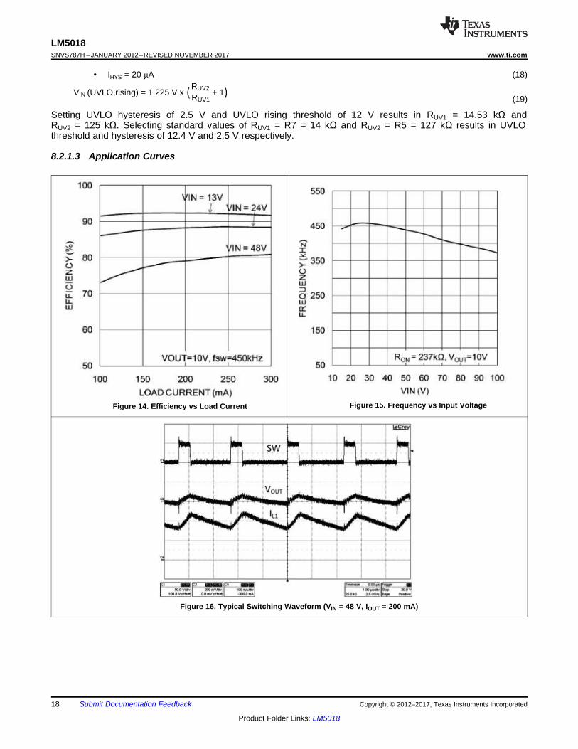
Figure 16. Typical Switching Waveform (VIN = 48 V, IOUT = 200 mA)
+
+
+
+
VIN
BST
RON
RTN
SW
VCC
FB
UVLO
VINVOUT1
VOUT2
RFB1
RUV1
RON
COUT1
CBST
D1
CIN
COUT2
RFB2
RUV2
X1
Rr
N1
N2
LM5018
CVCC+
D2
20V-95V
Cr
Cac
+CBYP
127 kΩ
8.25 kΩ
1 µF 0.1 µF130 kΩ
0.01 µF
1 µF
0.1 µF
7.32 kΩ
1 kΩ
1 µF
1 µF
1 nF46.4 kΩ
47 µH
NSVOUT2 = VOUT1 x NP- VF
19
LM5018www.ti.com SNVS787H –JANUARY 2012–REVISED NOVEMBER 2017
Product Folder Links: LM5018
Submit Documentation FeedbackCopyright © 2012–2017, Texas Instruments Incorporated
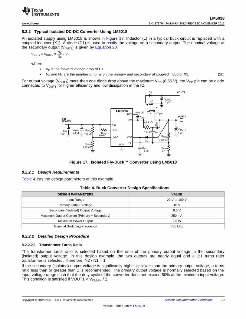
8.2.2 Typical Isolated DC-DC Converter Using LM5018An isolated supply using LM5018 is shown in Figure 17. Inductor (L) in a typical buck circuit is replaced with acoupled inductor (X1). A diode (D1) is used to rectify the voltage on a secondary output. The nominal voltage atthe secondary output (VOUT2) is given by Equation 20.
where• VF is the forward voltage drop of D1• NP and NS are the number of turns on the primary and secondary of coupled inductor X1. (20)
For output voltage (VOUT1) more than one diode drop above the maximum VCC (8.55 V), the VCC pin can be diodeconnected to VOUT1 for higher efficiency and low dissipation in the IC.
Figure 17. Isolated Fly-Buck™ Converter Using LM5018
8.2.2.1 Design RequirementsTable 4 lists the design parameters of this example.
Table 4. Buck Converter Design SpecificationsDESIGN PARAMETERS VALUE
Input Range 20 V to 100 VPrimary Output Voltage 10 V
Secondary (Isolated) Output Voltage 9.5 VMaximum Output Current (Primary + Secondary) 250 mA
Maximum Power Output 2.5 WNominal Switching Frequency 750 kHz
8.2.2.2 Detailed Design Procedure
8.2.2.2.1 Transformer Turns Ratio
The transformer turns ratio is selected based on the ratio of the primary output voltage to the secondary(isolated) output voltage. In this design example, the two outputs are nearly equal and a 1:1 turns ratiotransformer is selected. Therefore, N2 / N1 = 1.If the secondary (isolated) output voltage is significantly higher or lower than the primary output voltage, a turnsratio less than or greater than 1 is recommended. The primary output voltage is normally selected based on theinput voltage range such that the duty cycle of the converter does not exceed 50% at the minimum input voltage.This condition is satisfied if VOUT1 < VIN_MIN / 2.
'VOUT = 'IL1
x f x COUT1
f
S
IN(MAX) OUT OUT
L1 IN(MAX)W
V V VL1 42.6 H
I V¦
u P
' u
L1 OUT1 OUT2N2
I 0.39 A I I 2 0.28 AN1
§ ·' u u ¨ ¸
© ¹
VOUT1fSW = .x RON
x RFB1 = 7.16 k:VOUT1
:RFB2 = 1.225- 1)(
)RFB2VOUT1 = 1.225V x ( RFB11+
OUT(MAX) OUT1 OUT2N2
I I I 0.25 AN1
u
20
LM5018SNVS787H –JANUARY 2012–REVISED NOVEMBER 2017 www.ti.com
Product Folder Links: LM5018
Submit Documentation Feedback Copyright © 2012–2017, Texas Instruments Incorporated
8.2.2.2.2 Total IOUT
The total primary referred load current is calculated by multiplying the isolated output load(s) by the turns ratio ofthe transformer as shown in Equation 21.
(21)
8.2.2.2.3 RFB1, RFB2
The feedback resistors are selected to set the primary output voltage. The selected value for RFB1 is 1 kΩ. RFB2can be calculated using the following equations to set VOUT1 to the specified value of 10 V. A standard resistorvalue of 7.32 kΩ is selected for RFB2.
(22)
(23)
8.2.2.2.4 Frequency Selection
Equation 1 is used to calculate the value of RON required to achieve the desired switching frequency.
where• K = 9 × 10–11 (24)
For VOUT1 of 10 V and fSW of 750 kHz, the calculated value of RON is 148 kΩ. A lower value of 130 kΩ is selectedfor this design to allow for second order effects at high switching frequency that are not included in Equation 24.
8.2.2.2.5 Transformer Selection
A coupled inductor or a flyback-type transformer is required for this topology. Energy is transferred from primaryto secondary when the low-side synchronous switch of the buck converter is conducting.
The maximum inductor primary ripple current that can be tolerated without exceeding the buck switch peakcurrent limit threshold (0.39 A minimum) is given by Equation 25.
(25)
Using the maximum peak-to-peak inductor ripple current ΔIL1 from Equation 25, the minimum inductor value isgiven by Equation 26.
(26)
A higher value of 47 µH is selected to insure the high-side switch current does not exceed the minimum peakcurrent limit threshold.
8.2.2.2.6 Primary Output Capacitor
In a conventional buck converter, the output ripple voltage is calculated as shown in Equation 27.
(27)
To limit the primary output ripple voltage ΔVOUT1 to approximately 50 mV, an output capacitor COUT1 of 0.93 µF isrequired.
COUT2'VOUT2 =
IOUT2 x TON (MAX)
IL2
IOUT2
TON(MAX) x IOUT2
IL2
IOUT2
TON(MAX) x IOUT2
IL1
TON(MAX) x IOUT2 x N2/N1
OUT2 ON(MAX)
OUT1OUT1
N2I T
N1V 0.16 V
C
§ ·u u¨ ¸
© ¹' |
21
LM5018www.ti.com SNVS787H –JANUARY 2012–REVISED NOVEMBER 2017
Product Folder Links: LM5018
Submit Documentation FeedbackCopyright © 2012–2017, Texas Instruments Incorporated
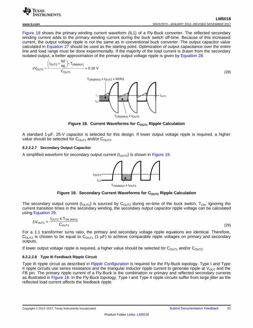
Figure 18 shows the primary winding current waveform (IL1) of a Fly-Buck converter. The reflected secondarywinding current adds to the primary winding current during the buck switch off-time. Because of this increasedcurrent, the output voltage ripple is not the same as in conventional buck converter. The output capacitor valuecalculated in Equation 27 should be used as the starting point. Optimization of output capacitance over the entireline and load range must be done experimentally. If the majority of the load current is drawn from the secondaryisolated output, a better approximation of the primary output voltage ripple is given by Equation 28.
(28)
Figure 18. Current Waveforms for COUT1 Ripple Calculation
A standard 1-µF, 25-V capacitor is selected for this design. If lower output voltage ripple is required, a highervalue should be selected for COUT1 and/or COUT2.
8.2.2.2.7 Secondary Output Capacitor
A simplified waveform for secondary output current (IOUT2) is shown in Figure 19.
Figure 19. Secondary Current Waveforms for COUT2 Ripple Calculation
The secondary output current (IOUT2) is sourced by COUT2 during on-time of the buck switch, TON. Ignoring thecurrent transition times in the secondary winding, the secondary output capacitor ripple voltage can be calculatedusing Equation 29.
(29)
For a 1:1 transformer turns ratio, the primary and secondary voltage ripple equations are identical. Therefore,COUT2 is chosen to be equal to COUT1 (1 µF) to achieve comparable ripple voltages on primary and secondaryoutputs.
If lower output voltage ripple is required, a higher value should be selected for COUT1 and/or COUT2.
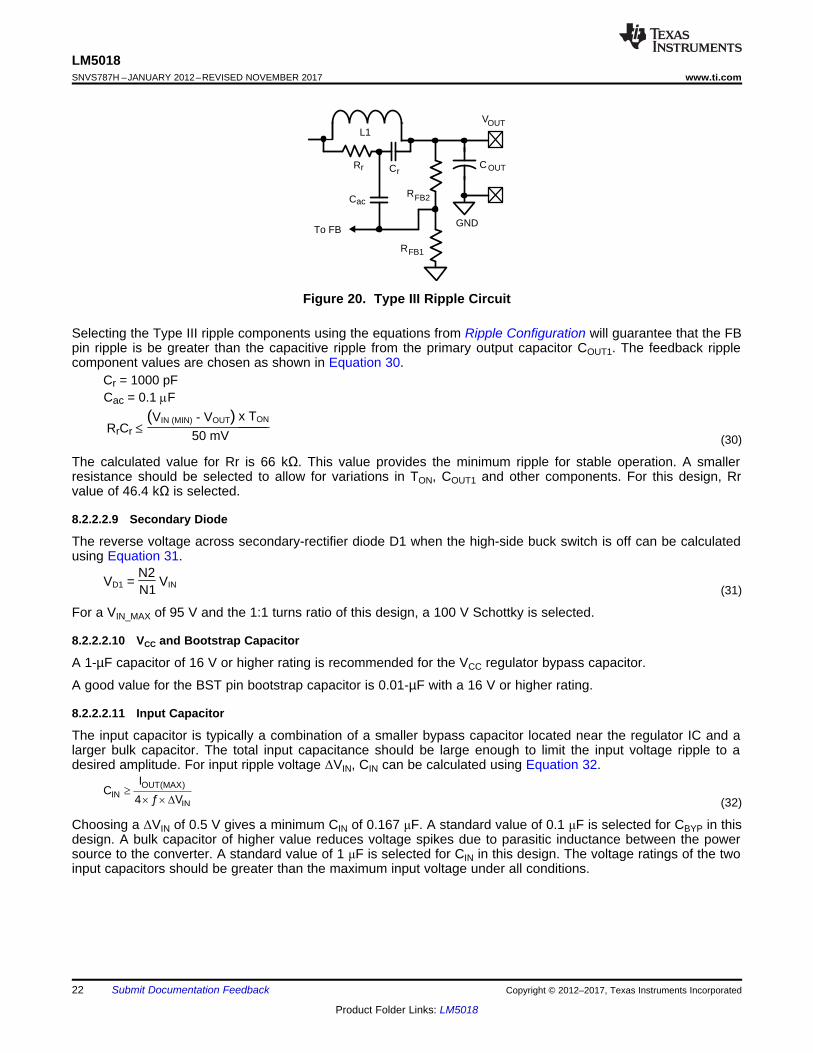
8.2.2.2.8 Type III Feedback Ripple Circuit
Type III ripple circuit as described in Ripple Configuration is required for the Fly-Buck topology. Type I and TypeII ripple circuits use series resistance and the triangular inductor ripple current to generate ripple at VOUT and theFB pin. The primary ripple current of a Fly-Buck is the combination or primary and reflected secondary currentsas illustrated in Figure 18. In the Fly-Buck topology, Type I and Type II ripple circuits suffer from large jitter as thereflected load current affects the feedback ripple.
OUT(MA
IN
X)IN
IC
4 ¦ 9u 't
u
N2N1
VD1 = VIN
Cr = 1000 pFCac = 0.1 PF
50 mVRrCr d
(VIN (MIN) - VOUT) x TON
GND
Rr
Cac
Cr
R
To FB
R
L1
FB1
FB2
COUT
VOUT
22
LM5018SNVS787H –JANUARY 2012–REVISED NOVEMBER 2017 www.ti.com
Product Folder Links: LM5018
Submit Documentation Feedback Copyright © 2012–2017, Texas Instruments Incorporated
Figure 20. Type III Ripple Circuit
Selecting the Type III ripple components using the equations from Ripple Configuration will guarantee that the FBpin ripple is be greater than the capacitive ripple from the primary output capacitor COUT1. The feedback ripplecomponent values are chosen as shown in Equation 30.
(30)
The calculated value for Rr is 66 kΩ. This value provides the minimum ripple for stable operation. A smallerresistance should be selected to allow for variations in TON, COUT1 and other components. For this design, Rrvalue of 46.4 kΩ is selected.
8.2.2.2.9 Secondary Diode
The reverse voltage across secondary-rectifier diode D1 when the high-side buck switch is off can be calculatedusing Equation 31.
(31)
For a VIN_MAX of 95 V and the 1:1 turns ratio of this design, a 100 V Schottky is selected.
8.2.2.2.10 VCC and Bootstrap Capacitor
A 1-µF capacitor of 16 V or higher rating is recommended for the VCC regulator bypass capacitor.
A good value for the BST pin bootstrap capacitor is 0.01-µF with a 16 V or higher rating.
8.2.2.2.11 Input Capacitor
The input capacitor is typically a combination of a smaller bypass capacitor located near the regulator IC and alarger bulk capacitor. The total input capacitance should be large enough to limit the input voltage ripple to adesired amplitude. For input ripple voltage ΔVIN, CIN can be calculated using Equation 32.
(32)
Choosing a ΔVIN of 0.5 V gives a minimum CIN of 0.167 μF. A standard value of 0.1 μF is selected for CBYP in thisdesign. A bulk capacitor of higher value reduces voltage spikes due to parasitic inductance between the powersource to the converter. A standard value of 1 μF is selected for CIN in this design. The voltage ratings of the twoinput capacitors should be greater than the maximum input voltage under all conditions.
VIN (UVLO, rising) = 1.225V x RUV2 + 1)(RUV1
VIN (HYS) = IHYS x RUV2
23
LM5018www.ti.com SNVS787H –JANUARY 2012–REVISED NOVEMBER 2017
Product Folder Links: LM5018
Submit Documentation FeedbackCopyright © 2012–2017, Texas Instruments Incorporated
8.2.2.2.12 UVLO Resistors
UVLO resistors RUV1 and RUV2 set the undervoltage lockout threshold and hysteresis according to Equation 33and Equation 34.
where• IHYS = 20 μA, typical. (33)
(34)
For a UVLO hysteresis of 2.5 V and UVLO rising threshold of 20 V, Equation 33 and Equation 34 require RUV1 of8.25 kΩ and RUV2 of 127 kΩ and these values are selected for this design example.
8.2.2.2.13 VCC Diode
Diode D2 is an optional diode connected between VOUT1 and the VCC regulator output pin. When VOUT1 is morethan one diode drop greater than the VCC voltage, the VCC bias current is supplied from VOUT1. This results inreduced power losses in the internal VCC regulator which improves converter efficiency. VOUT1 must be set to avoltage at least one diode drop higher than 8.55 V (the maximum VCC voltage) if D2 is used to supply biascurrent.
8.2.2.3 Application Curves
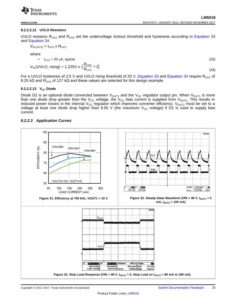
Figure 21. Efficiency at 750 kHz, VOUT1 = 10 V Figure 22. Steady-State Waveform (VIN = 48 V, IOUT1 = 0mA, IOUT2 = 100 mA)
Figure 23. Step Load Response (VIN = 48 V, IOUT1 = 0, Step Load on IOUT2 = 80 mA to 180 mA)
UVLO 3
RON 4
RTN 1
VIN 2
8 SW
7 BST
6 VCC
5 FB
SO PowerPAD-8
CIN
CVCC
24
LM5018SNVS787H –JANUARY 2012–REVISED NOVEMBER 2017 www.ti.com
Product Folder Links: LM5018
Submit Documentation Feedback Copyright © 2012–2017, Texas Instruments Incorporated
9 Power Supply RecommendationsLM5018 is a power management device. The power supply for the device is any DC voltage source within thespecified input range.
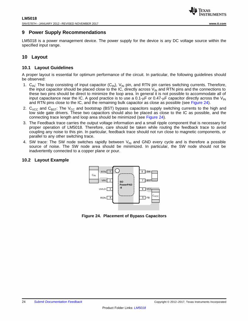
10 Layout
10.1 Layout GuidelinesA proper layout is essential for optimum performance of the circuit. In particular, the following guidelines shouldbe observed:1. CIN: The loop consisting of input capacitor (CIN), VIN pin, and RTN pin carries switching currents. Therefore,
the input capacitor should be placed close to the IC, directly across VIN and RTN pins and the connections tothese two pins should be direct to minimize the loop area. In general it is not possible to accommodate all ofinput capacitance near the IC. A good practice is to use a 0.1-μF or 0.47-μF capacitor directly across the VINand RTN pins close to the IC, and the remaining bulk capacitor as close as possible (see Figure 24).
2. CVCC and CBST: The VCC and bootstrap (BST) bypass capacitors supply switching currents to the high andlow side gate drivers. These two capacitors should also be placed as close to the IC as possible, and theconnecting trace length and loop area should be minimized (see Figure 24).
3. The Feedback trace carries the output voltage information and a small ripple component that is necessary forproper operation of LM5018. Therefore, care should be taken while routing the feedback trace to avoidcoupling any noise to this pin. In particular, feedback trace should not run close to magnetic components, orparallel to any other switching trace.
4. SW trace: The SW node switches rapidly between VIN and GND every cycle and is therefore a possiblesource of noise. The SW node area should be minimized. In particular, the SW node should not beinadvertently connected to a copper plane or pour.
10.2 Layout Example
Figure 24. Placement of Bypass Capacitors
25
LM5018www.ti.com SNVS787H –JANUARY 2012–REVISED NOVEMBER 2017
Product Folder Links: LM5018
Submit Documentation FeedbackCopyright © 2012–2017, Texas Instruments Incorporated
11 Device and Documentation Support
11.1 Device Support
11.1.1 Development Support
11.1.1.1 Custom Design With WEBENCH® ToolsClick here to create a custom design using the LM5018 device with the WEBENCH® Power Designer.1. Start by entering the input voltage (VIN), output voltage (VOUT), and output current (IOUT) requirements.2. Optimize the design for key parameters such as efficiency, footprint, and cost using the optimizer dial.3. Compare the generated design with other possible solutions from Texas Instruments.
The WEBENCH Power Designer provides a customized schematic along with a list of materials with real-timepricing and component availability.
In most cases, these actions are available:• Run electrical simulations to see important waveforms and circuit performance• Run thermal simulations to understand board thermal performance• Export customized schematic and layout into popular CAD formats• Print PDF reports for the design, and share the design with colleagues
Get more information about WEBENCH tools at www.ti.com/WEBENCH.
11.2 Documentation Support
11.2.1 Related Documentation• AN-2292 Designing an Isolated Buck (Flybuck) Converter (SNVA674)• AN-1481 Controlling Output Ripple and Achieving ESR Independence in Constant On-Time (COT) Regulator
Designs (SNVA166)• AN-2239 LM5018 Isolated Evaluation Board (SNVA667)
11.3 Receiving Notification of Documentation UpdatesTo receive notification of documentation updates, navigate to the device product folder on ti.com. In the upperright corner, click on Alert me to register and receive a weekly digest of any product information that haschanged. For change details, review the revision history included in any revised document.
11.4 Community ResourcesThe following links connect to TI community resources. Linked contents are provided "AS IS" by the respectivecontributors. They do not constitute TI specifications and do not necessarily reflect TI's views; see TI's Terms ofUse.
TI E2E™ Online Community TI's Engineer-to-Engineer (E2E) Community. Created to foster collaborationamong engineers. At e2e.ti.com, you can ask questions, share knowledge, explore ideas and helpsolve problems with fellow engineers.
Design Support TI's Design Support Quickly find helpful E2E forums along with design support tools andcontact information for technical support.
11.5 TrademarksPowerPAD, Fly-Buck, E2E are trademarks of Texas Instruments.WEBENCH is a registered trademark of Texas Instruments.All other trademarks are the property of their respective owners.
11.6 Electrostatic Discharge CautionThese devices have limited built-in ESD protection. The leads should be shorted together or the device placed in conductive foamduring storage or handling to prevent electrostatic damage to the MOS gates.
26
LM5018SNVS787H –JANUARY 2012–REVISED NOVEMBER 2017 www.ti.com
Product Folder Links: LM5018
Submit Documentation Feedback Copyright © 2012–2017, Texas Instruments Incorporated
11.7 GlossarySLYZ022 — TI Glossary.
This glossary lists and explains terms, acronyms, and definitions.
12 Mechanical, Packaging, and Orderable InformationThe following pages include mechanical, packaging, and orderable information. This information is the mostcurrent data available for the designated devices. This data is subject to change without notice and revision ofthis document. For browser-based versions of this data sheet, refer to the left-hand navigation.
PACKAGE OPTION ADDENDUM
www.ti.com 28-Nov-2017
Addendum-Page 1
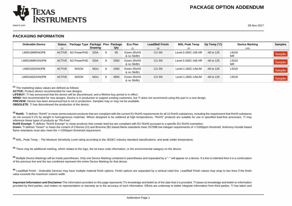
PACKAGING INFORMATION
Orderable Device Status(1)
Package Type PackageDrawing
Pins PackageQty
Eco Plan(2)
Lead/Ball Finish(6)
MSL Peak Temp(3)
Op Temp (°C) Device Marking(4/5)
Samples
LM5018MR/NOPB ACTIVE SO PowerPAD DDA 8 95 Green (RoHS& no Sb/Br)
CU SN Level-3-260C-168 HR -40 to 125 L5018MR
LM5018MRX/NOPB ACTIVE SO PowerPAD DDA 8 2500 Green (RoHS& no Sb/Br)
CU SN Level-3-260C-168 HR -40 to 125 L5018MR
LM5018SD/NOPB ACTIVE WSON NGU 8 1000 Green (RoHS& no Sb/Br)
CU SN Level-1-260C-UNLIM -40 to 125 L5018
LM5018SDX/NOPB ACTIVE WSON NGU 8 4500 Green (RoHS& no Sb/Br)
CU SN Level-1-260C-UNLIM -40 to 125 L5018
(1) The marketing status values are defined as follows:ACTIVE: Product device recommended for new designs.LIFEBUY: TI has announced that the device will be discontinued, and a lifetime-buy period is in effect.NRND: Not recommended for new designs. Device is in production to support existing customers, but TI does not recommend using this part in a new design.PREVIEW: Device has been announced but is not in production. Samples may or may not be available.OBSOLETE: TI has discontinued the production of the device.
(2) RoHS: TI defines "RoHS" to mean semiconductor products that are compliant with the current EU RoHS requirements for all 10 RoHS substances, including the requirement that RoHS substancedo not exceed 0.1% by weight in homogeneous materials. Where designed to be soldered at high temperatures, "RoHS" products are suitable for use in specified lead-free processes. TI mayreference these types of products as "Pb-Free".RoHS Exempt: TI defines "RoHS Exempt" to mean products that contain lead but are compliant with EU RoHS pursuant to a specific EU RoHS exemption.Green: TI defines "Green" to mean the content of Chlorine (Cl) and Bromine (Br) based flame retardants meet JS709B low halogen requirements of <=1000ppm threshold. Antimony trioxide basedflame retardants must also meet the <=1000ppm threshold requirement.
(3) MSL, Peak Temp. - The Moisture Sensitivity Level rating according to the JEDEC industry standard classifications, and peak solder temperature.
(4) There may be additional marking, which relates to the logo, the lot trace code information, or the environmental category on the device.
(5) Multiple Device Markings will be inside parentheses. Only one Device Marking contained in parentheses and separated by a "~" will appear on a device. If a line is indented then it is a continuationof the previous line and the two combined represent the entire Device Marking for that device.
(6) Lead/Ball Finish - Orderable Devices may have multiple material finish options. Finish options are separated by a vertical ruled line. Lead/Ball Finish values may wrap to two lines if the finishvalue exceeds the maximum column width.
Important Information and Disclaimer:The information provided on this page represents TI's knowledge and belief as of the date that it is provided. TI bases its knowledge and belief on informationprovided by third parties, and makes no representation or warranty as to the accuracy of such information. Efforts are underway to better integrate information from third parties. TI has taken and
PACKAGE OPTION ADDENDUM
www.ti.com 28-Nov-2017
Addendum-Page 2
continues to take reasonable steps to provide representative and accurate information but may not have conducted destructive testing or chemical analysis on incoming materials and chemicals.TI and TI suppliers consider certain information to be proprietary, and thus CAS numbers and other limited information may not be available for release.
In no event shall TI's liability arising out of such information exceed the total purchase price of the TI part(s) at issue in this document sold by TI to Customer on an annual basis.
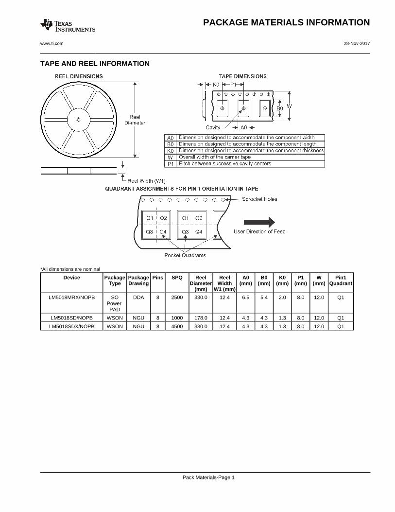
TAPE AND REEL INFORMATION
*All dimensions are nominal
Device PackageType
PackageDrawing
Pins SPQ ReelDiameter
(mm)
ReelWidth
W1 (mm)
A0(mm)
B0(mm)
K0(mm)
P1(mm)
W(mm)
Pin1Quadrant
LM5018MRX/NOPB SOPower PAD
DDA 8 2500 330.0 12.4 6.5 5.4 2.0 8.0 12.0 Q1
LM5018SD/NOPB WSON NGU 8 1000 178.0 12.4 4.3 4.3 1.3 8.0 12.0 Q1
LM5018SDX/NOPB WSON NGU 8 4500 330.0 12.4 4.3 4.3 1.3 8.0 12.0 Q1
PACKAGE MATERIALS INFORMATION
www.ti.com 28-Nov-2017
Pack Materials-Page 1
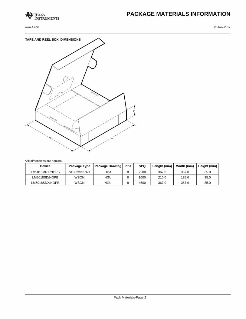
*All dimensions are nominal
Device Package Type Package Drawing Pins SPQ Length (mm) Width (mm) Height (mm)
LM5018MRX/NOPB SO PowerPAD DDA 8 2500 367.0 367.0 35.0
LM5018SD/NOPB WSON NGU 8 1000 210.0 185.0 35.0
LM5018SDX/NOPB WSON NGU 8 4500 367.0 367.0 35.0
PACKAGE MATERIALS INFORMATION
www.ti.com 28-Nov-2017
Pack Materials-Page 2
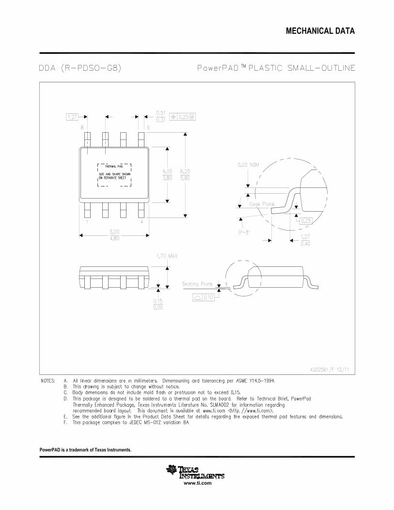
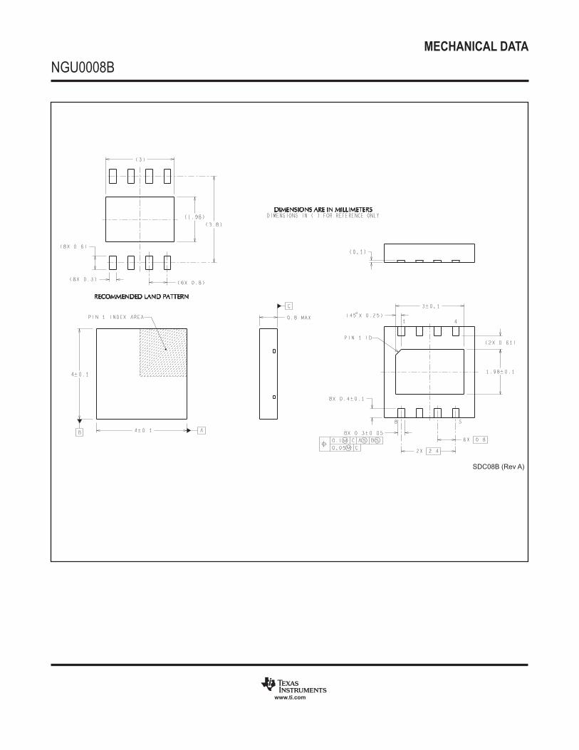
MECHANICAL DATA
NGU0008B
www.ti.com
SDC08B (Rev A)
IMPORTANT NOTICE
Texas Instruments Incorporated (TI) reserves the right to make corrections, enhancements, improvements and other changes to itssemiconductor products and services per JESD46, latest issue, and to discontinue any product or service per JESD48, latest issue. Buyersshould obtain the latest relevant information before placing orders and should verify that such information is current and complete.TI’s published terms of sale for semiconductor products (http://www.ti.com/sc/docs/stdterms.htm) apply to the sale of packaged integratedcircuit products that TI has qualified and released to market. Additional terms may apply to the use or sale of other types of TI products andservices.Reproduction of significant portions of TI information in TI data sheets is permissible only if reproduction is without alteration and isaccompanied by all associated warranties, conditions, limitations, and notices. TI is not responsible or liable for such reproduceddocumentation. Information of third parties may be subject to additional restrictions. Resale of TI products or services with statementsdifferent from or beyond the parameters stated by TI for that product or service voids all express and any implied warranties for theassociated TI product or service and is an unfair and deceptive business practice. TI is not responsible or liable for any such statements.Buyers and others who are developing systems that incorporate TI products (collectively, “Designers”) understand and agree that Designersremain responsible for using their independent analysis, evaluation and judgment in designing their applications and that Designers havefull and exclusive responsibility to assure the safety of Designers' applications and compliance of their applications (and of all TI productsused in or for Designers’ applications) with all applicable regulations, laws and other applicable requirements. Designer represents that, withrespect to their applications, Designer has all the necessary expertise to create and implement safeguards that (1) anticipate dangerousconsequences of failures, (2) monitor failures and their consequences, and (3) lessen the likelihood of failures that might cause harm andtake appropriate actions. Designer agrees that prior to using or distributing any applications that include TI products, Designer willthoroughly test such applications and the functionality of such TI products as used in such applications.TI’s provision of technical, application or other design advice, quality characterization, reliability data or other services or information,including, but not limited to, reference designs and materials relating to evaluation modules, (collectively, “TI Resources”) are intended toassist designers who are developing applications that incorporate TI products; by downloading, accessing or using TI Resources in anyway, Designer (individually or, if Designer is acting on behalf of a company, Designer’s company) agrees to use any particular TI Resourcesolely for this purpose and subject to the terms of this Notice.TI’s provision of TI Resources does not expand or otherwise alter TI’s applicable published warranties or warranty disclaimers for TIproducts, and no additional obligations or liabilities arise from TI providing such TI Resources. TI reserves the right to make corrections,enhancements, improvements and other changes to its TI Resources. TI has not conducted any testing other than that specificallydescribed in the published documentation for a particular TI Resource.Designer is authorized to use, copy and modify any individual TI Resource only in connection with the development of applications thatinclude the TI product(s) identified in such TI Resource. NO OTHER LICENSE, EXPRESS OR IMPLIED, BY ESTOPPEL OR OTHERWISETO ANY OTHER TI INTELLECTUAL PROPERTY RIGHT, AND NO LICENSE TO ANY TECHNOLOGY OR INTELLECTUAL PROPERTYRIGHT OF TI OR ANY THIRD PARTY IS GRANTED HEREIN, including but not limited to any patent right, copyright, mask work right, orother intellectual property right relating to any combination, machine, or process in which TI products or services are used. Informationregarding or referencing third-party products or services does not constitute a license to use such products or services, or a warranty orendorsement thereof. Use of TI Resources may require a license from a third party under the patents or other intellectual property of thethird party, or a license from TI under the patents or other intellectual property of TI.TI RESOURCES ARE PROVIDED “AS IS” AND WITH ALL FAULTS. TI DISCLAIMS ALL OTHER WARRANTIES ORREPRESENTATIONS, EXPRESS OR IMPLIED, REGARDING RESOURCES OR USE THEREOF, INCLUDING BUT NOT LIMITED TOACCURACY OR COMPLETENESS, TITLE, ANY EPIDEMIC FAILURE WARRANTY AND ANY IMPLIED WARRANTIES OFMERCHANTABILITY, FITNESS FOR A PARTICULAR PURPOSE, AND NON-INFRINGEMENT OF ANY THIRD PARTY INTELLECTUALPROPERTY RIGHTS. TI SHALL NOT BE LIABLE FOR AND SHALL NOT DEFEND OR INDEMNIFY DESIGNER AGAINST ANY CLAIM,INCLUDING BUT NOT LIMITED TO ANY INFRINGEMENT CLAIM THAT RELATES TO OR IS BASED ON ANY COMBINATION OFPRODUCTS EVEN IF DESCRIBED IN TI RESOURCES OR OTHERWISE. IN NO EVENT SHALL TI BE LIABLE FOR ANY ACTUAL,DIRECT, SPECIAL, COLLATERAL, INDIRECT, PUNITIVE, INCIDENTAL, CONSEQUENTIAL OR EXEMPLARY DAMAGES INCONNECTION WITH OR ARISING OUT OF TI RESOURCES OR USE THEREOF, AND REGARDLESS OF WHETHER TI HAS BEENADVISED OF THE POSSIBILITY OF SUCH DAMAGES.Unless TI has explicitly designated an individual product as meeting the requirements of a particular industry standard (e.g., ISO/TS 16949and ISO 26262), TI is not responsible for any failure to meet such industry standard requirements.Where TI specifically promotes products as facilitating functional safety or as compliant with industry functional safety standards, suchproducts are intended to help enable customers to design and create their own applications that meet applicable functional safety standardsand requirements. Using products in an application does not by itself establish any safety features in the application. Designers mustensure compliance with safety-related requirements and standards applicable to their applications. Designer may not use any TI products inlife-critical medical equipment unless authorized officers of the parties have executed a special contract specifically governing such use.Life-critical medical equipment is medical equipment where failure of such equipment would cause serious bodily injury or death (e.g., lifesupport, pacemakers, defibrillators, heart pumps, neurostimulators, and implantables). Such equipment includes, without limitation, allmedical devices identified by the U.S. Food and Drug Administration as Class III devices and equivalent classifications outside the U.S.TI may expressly designate certain products as completing a particular qualification (e.g., Q100, Military Grade, or Enhanced Product).Designers agree that it has the necessary expertise to select the product with the appropriate qualification designation for their applicationsand that proper product selection is at Designers’ own risk. Designers are solely responsible for compliance with all legal and regulatoryrequirements in connection with such selection.Designer will fully indemnify TI and its representatives against any damages, costs, losses, and/or liabilities arising out of Designer’s non-compliance with the terms and provisions of this Notice.
Mailing Address: Texas Instruments, Post Office Box 655303, Dallas, Texas 75265Copyright © 2018, Texas Instruments Incorporated