Embed Size (px)
Citation preview
Copyright © 2016, Texas Instruments Incorporated
RT/SD
FB
VIN
SW
RTN
BST
6V - 95V
Input
LM5008A
SHUTDOWN
RCL
VCCVIN
GND
RCL
RT
C1 C3
C4 L1
D1
RFB2
RFB1
R3
C2
GND
VOUT
Product
Folder
Order
Now
Technical
Documents
Tools &
Software
Support &Community
An IMPORTANT NOTICE at the end of this data sheet addresses availability, warranty, changes, use in safety-critical applications,intellectual property matters and other important disclaimers. PRODUCTION DATA.
LM5008ASNVS583G –MARCH 2009–REVISED DECEMBER 2016
LM5008A 100-V 350-mA Constant On-Time Buck Switching Regulator
1
1 Features1• Operating Input Voltage Range: 6 V to 95 V• Integrated 100-V N-Channel Buck Switch• Internal Start-Up Regulator• No Loop Compensation Required• Ultra-Fast Transient Response• On-Time Varies Inversely With Input Voltage• Operating Frequency Remains Constant With
Varying Line Voltage and Load Current• Adjustable Output Voltage From 2.5 V• Highly Efficient Operation• Precision Internal Reference• Low Bias Current• Intelligent Current Limit• Thermal Shutdown• 8-Pin VSSOP and 8-Pin WSON Packages
2 Applications• Non-Isolated Telecommunication Buck Regulators• Secondary High Voltage Post Regulators• 42-V Automotive Systems
3 DescriptionThe LM5008A device is a functional variant of theLM5008 COT Buck Switching Regulator. Thefunctional differences of the LM5008A are: theminimum input operating voltage is 6 V, the on-timeequation is slightly different, and the requirement fora minimum load current is removed.
The LM5008A step-down switching regulator featuresall of the functions required to implement a low-cost,efficient, Buck bias regulator. This high voltageregulator contains an 100-V N-channel buck switch.The device is easy to implement and is provided inthe 8-pin VSSOP and the thermally enhanced 8-pinWSON packages. The regulator is based on a controlscheme using an on-time inversely proportional toVIN. This feature allows the operating frequency toremain relatively constant. The control schemerequires no loop compensation. An intelligent currentlimit is implemented with forced off-time, which isinversely proportional to VOUT. This scheme ensuresshort-circuit control while providing minimumfoldback. Other features include: thermal shutdown,VCC undervoltage lockout, gate drive undervoltagelockout, maximum duty cycle limiter, and a pre-charge switch.
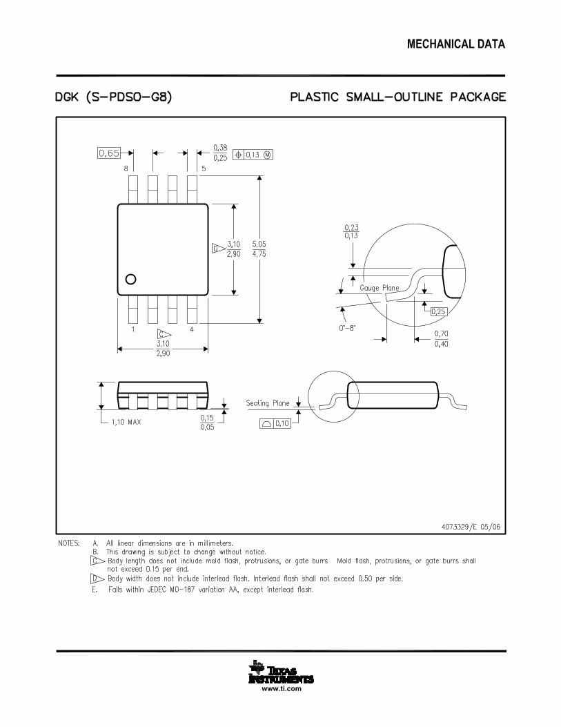
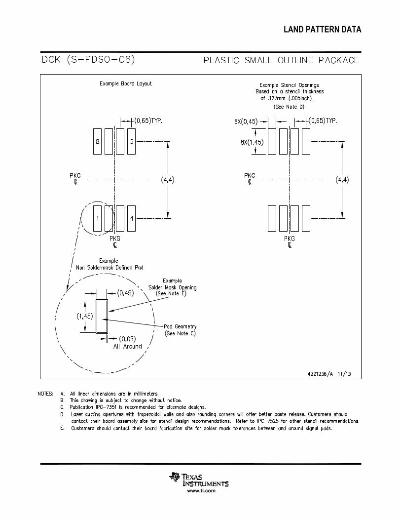
Device Information(1)
PART NUMBER PACKAGE BODY SIZE (NOM)
LM5008AVSSOP (8) 4.00 mm × 4.00 mmWSON (8) 4.00 mm × 4.00 mm
(1) For all available packages, see the orderable addendum atthe end of the data sheet.
Typical Application, Basic Step-Down Regulator
2
LM5008ASNVS583G –MARCH 2009–REVISED DECEMBER 2016 www.ti.com
Product Folder Links: LM5008A
Submit Documentation Feedback Copyright © 2009–2016, Texas Instruments Incorporated
Table of Contents1 Features .................................................................. 12 Applications ........................................................... 13 Description ............................................................. 14 Revision History..................................................... 25 Pin Configuration and Functions ......................... 36 Specifications......................................................... 3
6.1 Absolute Maximum Ratings ...................................... 36.2 ESD Ratings ............................................................ 46.3 Recommended Operating Conditions....................... 46.4 Thermal Information ................................................. 46.5 Electrical Characteristics........................................... 46.6 Switching Characteristics .......................................... 56.7 Typical Characteristics .............................................. 6
7 Detailed Description .............................................. 77.1 Overview ................................................................... 77.2 Functional Block Diagram ......................................... 77.3 Feature Description................................................... 7
7.4 Device Functional Modes........................................ 118 Application and Implementation ........................ 12
8.1 Application Information............................................ 128.2 Typical Application .................................................. 12
9 Power Supply Recommendations ...................... 1610 Layout................................................................... 17
10.1 Layout Guidelines ................................................. 1710.2 Layout Examples................................................... 17
11 Device and Documentation Support ................. 1911.1 Device Support .................................................... 1911.2 Documentation Support ........................................ 1911.3 Receiving Notification of Documentation Updates 1911.4 Community Resources.......................................... 1911.5 Trademarks ........................................................... 2011.6 Electrostatic Discharge Caution............................ 2011.7 Glossary ................................................................ 20
12 Mechanical, Packaging, and OrderableInformation ........................................................... 20
4 Revision HistoryNOTE: Page numbers for previous revisions may differ from page numbers in the current version.
Changes from Revision F (March 2013) to Revision G Page
• Added ESD Ratings table, Feature Description section, Device Functional Modes, Application and Implementationsection, Power Supply Recommendations section, Layout section, Device and Documentation Support section, andMechanical, Packaging, and Orderable Information section .................................................................................................. 1
• Deleted Lead temperature (260°C maximum)........................................................................................................................ 3• Changed RθJA value From: 200°C/W To: 139.7°C/W (VSSOP) and From: 40°C/W To: 42°C/W (WSON)............................ 4
Changes from Revision E (March 2013) to Revision F Page
• Changed layout of National Data Sheet to TI format ........................................................................................................... 16
1SW 8 VIN
2BST 7 VCC
3RCL 6 RT/SD
4RTN 5 FB
Not to scale
1SW 8 VIN
2BST 7 VCC
3RCL 6 RT/SD
4RTN 5 FB
Not to scale
EP
3
LM5008Awww.ti.com SNVS583G –MARCH 2009–REVISED DECEMBER 2016
Product Folder Links: LM5008A
Submit Documentation FeedbackCopyright © 2009–2016, Texas Instruments Incorporated
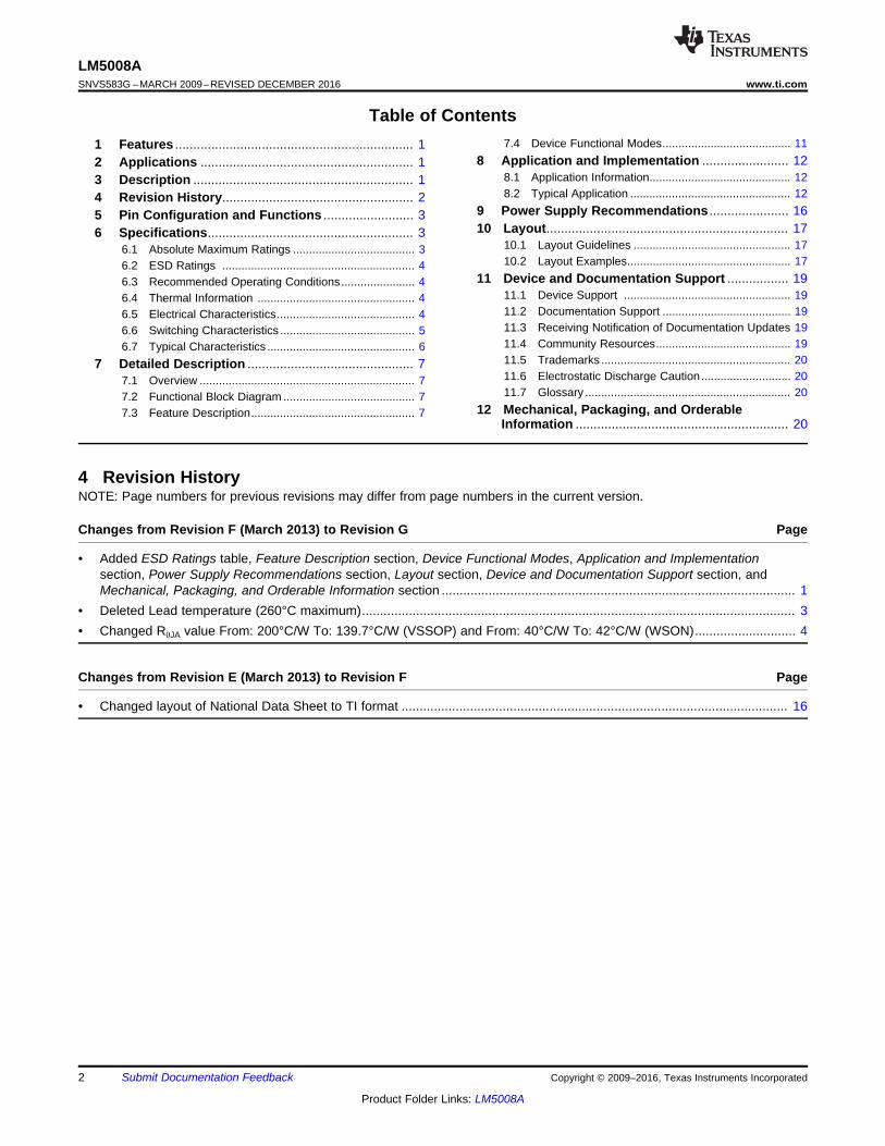
5 Pin Configuration and Functions
DGK Package8-Pin VSSOP
Top View
NGU Package8-Pin WSON
Top View
Pin FunctionsPIN
TYPE DESCRIPTIONNO. NAME
1 SW P Switching node: power switching node. Connect to the output inductor, re-circulating diode, and bootstrapcapacitor.
2 BST IBoost pin (bootstrap capacitor input): an external capacitor is required between the BST and the SW pins. A0.01-µF ceramic capacitor is recommended. An internal diode charges the capacitor from VCC during eachoff-time.
3 RCL I Current limit off-time set pin: a resistor between this pin and RTN sets the off-time when current limit isdetected. The off-time is preset to 35 µs if FB = 0 V.
4 RTN G Ground pin: ground for the entire circuit.
5 FB I Feedback input from regulated output: this pin is connected to the inverting input of the internal regulationcomparator. The regulation threshold is 2.5 V.
6 RT/SD IOn-time set pin: a resistor between this pin and VIN sets the switch on time as a function of VIN. Theminimum recommended on time is 400 ns at the maximum input voltage. This pin can be used for remoteshutdown.
7 VCC POutput from the internal high voltage series pass regulator: this regulated voltage provides gate drive powerfor the internal buck switch. An internal diode is provided between this pin and the BST pin. A local 0.47-µFdecoupling capacitor is required. The series pass regulator is current limited to 9 mA.
8 VIN P Input voltage: input operating range from 6 V to 95 V.
— EP G Exposed pad: the exposed pad has no electrical contact. Connect to system ground plane for reducedthermal resistance. (WSON package only)
(1) Stresses beyond those listed under Absolute Maximum Ratings may cause permanent damage to the device. These are stress ratingsonly, which do not imply functional operation of the device at these or any other conditions beyond those indicated under RecommendedOperating Conditions. Exposure to absolute-maximum-rated conditions for extended periods may affect device reliability.
6 Specifications
6.1 Absolute Maximum Ratingsover operating free-air temperature range (unless otherwise noted) (1)
MIN MAX UNITVIN to GND –0.3 100 VBST to GND –0.3 114 VSW to GND (steady-state) –1 VBST to VCC 100 VBST to SW 14 VVCC to GND 14 VAll other inputs to GND –0.3 7 VStorage temperature, Tstg –55 150 °C
4
LM5008ASNVS583G –MARCH 2009–REVISED DECEMBER 2016 www.ti.com
Product Folder Links: LM5008A
Submit Documentation Feedback Copyright © 2009–2016, Texas Instruments Incorporated
(1) JEDEC document JEP155 states that 500-V HBM allows safe manufacturing with a standard ESD control process.(2) JEDEC document JEP157 states that 250-V CDM allows safe manufacturing with a standard ESD control process.
6.2 ESD RatingsVALUE UNIT
V(ESD) Electrostatic dischargeHuman-body model (HBM), per ANSI/ESDA/JEDEC JS-001 (1) ±2000
VCharged-device model (CDM), per JEDEC specification JESD22-C101 (2) ±750
6.3 Recommended Operating Conditionsover operating free-air temperature range (unless otherwise noted)
MIN MAX UNITVIN 6 95 VOperating junction temperature –40 125 °C
(1) For more information about traditional and new thermal metrics, see the Semiconductor and IC Package Thermal Metrics applicationreport.
6.4 Thermal Information
THERMAL METRIC (1)LM5008A
UNITDGK (VSSOP) NGU (WSON)8 PINS 8 PINS
RθJA Junction-to-ambient thermal resistance 139.7 42 °C/WRθJC(top) Junction-to-case (top) thermal resistance 51.2 27.6 °C/WRθJB Junction-to-board thermal resistance 70.5 18.5 °C/WψJT Junction-to-top characterization parameter 3.4 0.3 °C/WψJB Junction-to-board characterization parameter 69.5 18.5 °C/WRθJC(bot) Junction-to-case (bottom) thermal resistance — 4.3 °C/W
(1) All electrical characteristics having room temperature limits are tested during production with TA = TJ = 25°C. All hot and cold limits arespecified by correlating the electrical characteristics to process and temperature variations and applying statistical process control.
6.5 Electrical CharacteristicsTJ = 25°C, and VIN = 48 V (unless otherwise noted) (1)
PARAMETER TEST CONDITIONS MIN TYP MAX UNITVCC SUPPLY
VCC Reg VCC regulator output VIN = 48 VTJ = 25°C 7
VTJ = –40°C to 125°C 6.6 7.4
VIN – VCC 6 V < VIN < 8.5 V 100 mVVCC bypass threshold VIN increasing 8.5 VVCC bypass hysteresis 300 mV
VCC output impedanceVIN = 6 V 100 Ω
VIN = 10 V 8.8 Ω
VIN = 48 V 0.8 Ω
VCC current limit VIN = 48 V 9.2 mAVCC UVLO VCC increasing 5.3 VVCC UVLO hysteresis 190 mVVCC UVLO filter delay 3 µs
IIN operating current FB = 3 V, VIN = 48 VTJ = 25°C 550
µATJ = –40°C to 125°C 750
IIN shutdown current RT/SD = 0 VTJ = 25°C 110
µATJ = –40°C to 125°C 176
5
LM5008Awww.ti.com SNVS583G –MARCH 2009–REVISED DECEMBER 2016
Product Folder Links: LM5008A
Submit Documentation FeedbackCopyright © 2009–2016, Texas Instruments Incorporated
Electrical Characteristics (continued)TJ = 25°C, and VIN = 48 V (unless otherwise noted)(1)
PARAMETER TEST CONDITIONS MIN TYP MAX UNITCURRENT LIMIT
Current limit thresholdTJ = 25°C 0.51
ATJ = –40°C to 125°C 0.41 0.61
Current limit response time Iswitch overdrive = 0.1 A, time to switch off 350 nsTOFF-1 Off-time generator FB = 0 V, RCL = 100 K 35 µsTOFF-2 Off-time generator FB = 2.3 V, RCL = 100 K 2.56 µsON-TIME GENERATOR
TON – 1 VIN = 10 V, RON = 200 KTJ = 25°C 2.77
µsTJ = –40°C to 125°C 2.15 3.5
TON – 2 VIN = 95 V, RON = 200 KTJ = 25°C 300
nsTJ = –40°C to 125°C 200 420
Remote shutdownthreshold Rising
TJ = 25°C 0.7V
TJ = –40°C to 125°C 0.4 1.05Remote shutdownhysteresis 35 mV
MINIMUM OFF-TIMEMinimum off-timer FB = 0 V 300 ns
REGULATION AND OV COMPARATORS
FB reference threshold Internal reference, trip point forswitch ON
TJ = 25°C 2.5V
TJ = –40°C to 125°C 2.445 2.55FB overvoltage threshold Trip point for switch OFF 2.875 VFB bias current 100 nA
THERMAL SHUTDOWN
Tsd Thermal shutdowntemperature 165 °C
Thermal shutdownhysteresis 25 °C
6.6 Switching Characteristicsover operating free-air temperature range (unless otherwise noted)
PARAMETER TEST CONDITIONS MIN TYP MAX UNIT
Buck switch RDS(on) ITEST = 200 mATJ = 25°C 1.25
ΩTJ = –40°C to 125°C 2.57
Gate drive UVLO VBST – VSW risingTJ = 25°C 3.8
VTJ = –40°C to 125°C 2.8 4.8
Gate drive UVLO hysteresis 490 mVPre-charge switch voltage At 1 mA 0.8 VPre-charge switch on-time 150 ns
0 0.5 1.0 1.5 2.0 2.5
0
5
10
15
20
25
30
35
CU
RR
EN
T L
IMIT
OF
F T
IME
(P
s)
VFB (V)
300kRCL = 500k
100k
50k
6
LM5008ASNVS583G –MARCH 2009–REVISED DECEMBER 2016 www.ti.com
Product Folder Links: LM5008A
Submit Documentation Feedback Copyright © 2009–2016, Texas Instruments Incorporated
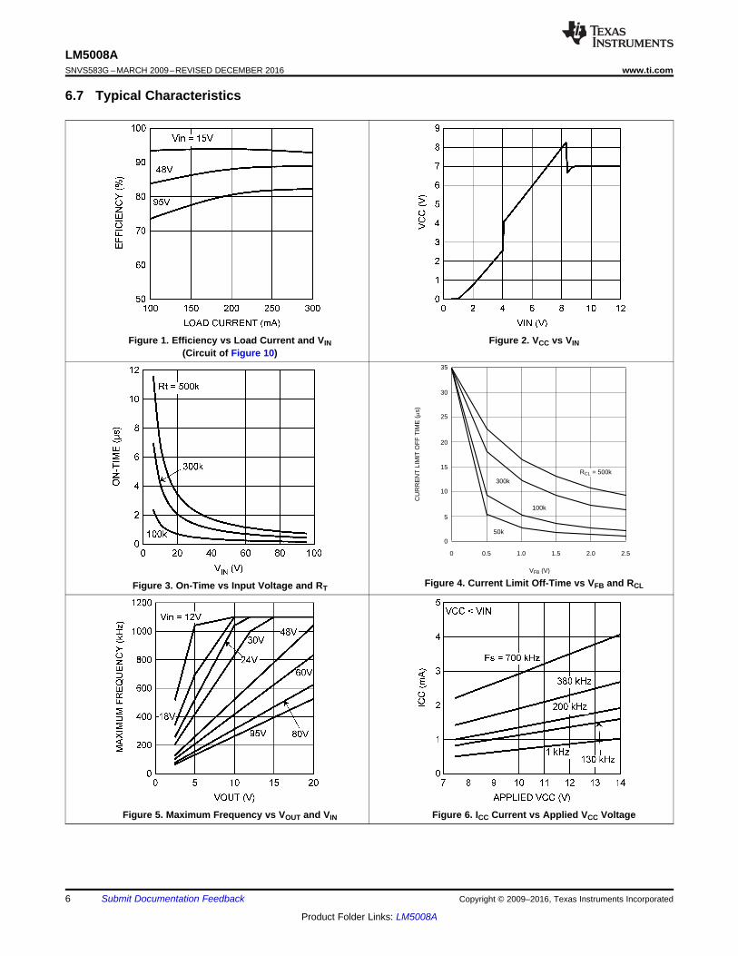
6.7 Typical Characteristics
Figure 1. Efficiency vs Load Current and VIN(Circuit of Figure 10)
Figure 2. VCC vs VIN
Figure 3. On-Time vs Input Voltage and RT Figure 4. Current Limit Off-Time vs VFB and RCL
Figure 5. Maximum Frequency vs VOUT and VIN Figure 6. ICC Current vs Applied VCC Voltage
Copyright © 2016, Texas Instruments Incorporated
Q
QFB
VIN
VCC
SW
RTN
ON TIMER
DRIVER
Vin
BST
LEVEL
SHIFT
THERMALSHUTDOWN
FINISH
START
RCL FINISH
START
RT
L1
R
VCCUVLO
FB
D1
UVLO
REGULATIONCOMPARATOR
SD
FINISH
START
REGULATOR
CURRENT LIMITOFF TIMER
SHUTDOWN GD
BUCKSWITCH
CURRENTSENSE
GND
LM5008A7V BIAS
BYPASSSWITCH
RT
2.875V
VINSENSEQ2
C1 C5
6V to 95VInput
RT/SD
0.7V
300 ns MIN
OFF TIMER
CLRR
SETS
0.51AC2
C3
VOUT
R3
RFB1
FB2
RCL
RCL
2.5V
OVER-VOLTAGECOMPARATOR
CHARGEPRE -
C4
7
LM5008Awww.ti.com SNVS583G –MARCH 2009–REVISED DECEMBER 2016
Product Folder Links: LM5008A
Submit Documentation FeedbackCopyright © 2009–2016, Texas Instruments Incorporated
7 Detailed Description
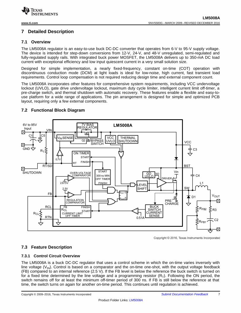
7.1 OverviewThe LM5008A regulator is an easy-to-use buck DC-DC converter that operates from 6-V to 95-V supply voltage.The device is intended for step-down conversions from 12-V, 24-V, and 48-V unregulated, semi-regulated andfully-regulated supply rails. With integrated buck power MOSFET, the LM5008A delivers up to 350-mA DC loadcurrent with exceptional efficiency and low input quiescent current in a very small solution size.
Designed for simple implementation, a nearly fixed-frequency, constant on-time (COT) operation withdiscontinuous conduction mode (DCM) at light loads is ideal for low-noise, high current, fast transient loadrequirements. Control loop compensation is not required reducing design time and external component count.
The LM5008A incorporates other features for comprehensive system requirements, including VCC undervoltagelockout (UVLO), gate drive undervoltage lockout, maximum duty cycle limiter, intelligent current limit off-timer, apre-charge switch, and thermal shutdown with automatic recovery. These features enable a flexible and easy-to-use platform for a wide range of applications. The pin arrangement is designed for simple and optimized PCBlayout, requiring only a few external components.
7.2 Functional Block Diagram
7.3 Feature Description
7.3.1 Control Circuit OverviewThe LM5008A is a buck DC-DC regulator that uses a control scheme in which the on-time varies inversely withline voltage (VIN). Control is based on a comparator and the on-time one-shot, with the output voltage feedback(FB) compared to an internal reference (2.5 V). If the FB level is below the reference the buck switch is turned onfor a fixed time determined by the line voltage and a programming resistor (RT). Following the ON period, theswitch remains off for at least the minimum off-timer period of 300 ns. If FB is still below the reference at thattime, the switch turns on again for another on-time period. This continues until regulation is achieved.
Copyright © 2016, Texas Instruments Incorporated
FB
SW
L1
C2
RFB2
VOUT2
R3LM5008A
RFB1
OUT10
T
VF
1.385 10 R�
u u
2 20OUT
2L T
V L 1.04 10F
R (R )
u u u
u
8
LM5008ASNVS583G –MARCH 2009–REVISED DECEMBER 2016 www.ti.com
Product Folder Links: LM5008A
Submit Documentation Feedback Copyright © 2009–2016, Texas Instruments Incorporated
Feature Description (continued)The LM5008A operates in discontinuous conduction mode at light load currents, and continuous conductionmode at heavy load current. In discontinuous conduction mode, current through the output inductor starts at zeroand ramps up to a peak during the on-time, then ramps back to zero before the end of the off-time. The next on-time period starts when the voltage at FB falls below the internal reference; until then, the inductor currentremains zero. In this mode, the operating frequency is lower than in continuous conduction mode and varies withload current. Therefore, at light loads, the conversion efficiency is maintained because the switching lossesreduce with the reduction in load and frequency. The discontinuous operating frequency can be calculated withEquation 1.
where• RL = the load resistance (1)
In continuous conduction mode, current flows continuously through the inductor and never ramps down to zero.In this mode the operating frequency is greater than the discontinuous mode frequency and remains relativelyconstant with load and line variations. The approximate continuous mode operating frequency can be calculatedwith Equation 2.
(2)
The output voltage (VOUT) is programmed by two external resistors as shown in the Functional Block Diagram.The regulation point can be calculated with Equation 3.
VOUT = 2.5 × (RFB1 + RFB2) / RFB1 (3)
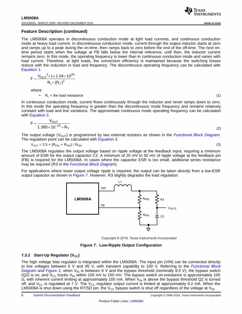
The LM5008A regulates the output voltage based on ripple voltage at the feedback input, requiring a minimumamount of ESR for the output capacitor C2. A minimum of 25 mV to 50 mV of ripple voltage at the feedback pin(FB) is required for the LM5008A. In cases where the capacitor ESR is too small, additional series resistancemay be required (R3 in the Functional Block Diagram).
For applications where lower output voltage ripple is required, the output can be taken directly from a low-ESRoutput capacitor as shown in Figure 7. However, R3 slightly degrades the load regulation.
Figure 7. Low-Ripple Output Configuration
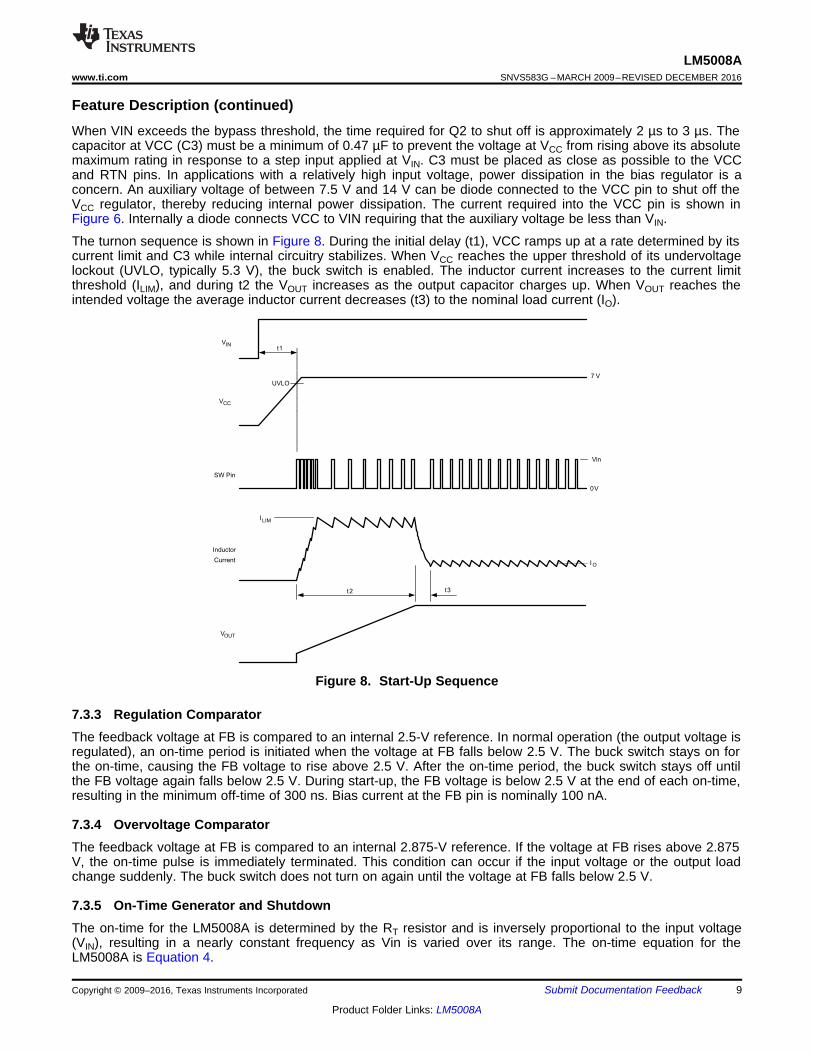
7.3.2 Start-Up Regulator (VCC)The high voltage bias regulator is integrated within the LM5008A. The input pin (VIN) can be connected directlyto line voltages between 6 V and 95 V, with transient capability to 100 V. Referring to the Functional BlockDiagram and Figure 2, when VIN is between 6 V and the bypass threshold (nominally 8.5 V), the bypass switch(Q2) is on, and VCC tracks VIN within 100 mV to 150 mV. The bypass switch on-resistance is approximately 100Ω, with inherent current limiting at approximately 100 mA. When VIN is above the bypass threshold Q2 is turnedoff, and VCC is regulated at 7 V. The VCC regulator output current is limited at approximately 9.2 mA. When theLM5008A is shut down using the RT/SD pin, the VCC bypass switch is shut off regardless of the voltage at VIN.
UVLO
7 V
SW Pin
Inductor
Current
Vin
t2
ILIM
VCC
VINt1
t3
I O
0V
VOUT
9
LM5008Awww.ti.com SNVS583G –MARCH 2009–REVISED DECEMBER 2016
Product Folder Links: LM5008A
Submit Documentation FeedbackCopyright © 2009–2016, Texas Instruments Incorporated
Feature Description (continued)When VIN exceeds the bypass threshold, the time required for Q2 to shut off is approximately 2 µs to 3 µs. Thecapacitor at VCC (C3) must be a minimum of 0.47 µF to prevent the voltage at VCC from rising above its absolutemaximum rating in response to a step input applied at VIN. C3 must be placed as close as possible to the VCCand RTN pins. In applications with a relatively high input voltage, power dissipation in the bias regulator is aconcern. An auxiliary voltage of between 7.5 V and 14 V can be diode connected to the VCC pin to shut off theVCC regulator, thereby reducing internal power dissipation. The current required into the VCC pin is shown inFigure 6. Internally a diode connects VCC to VIN requiring that the auxiliary voltage be less than VIN.
The turnon sequence is shown in Figure 8. During the initial delay (t1), VCC ramps up at a rate determined by itscurrent limit and C3 while internal circuitry stabilizes. When VCC reaches the upper threshold of its undervoltagelockout (UVLO, typically 5.3 V), the buck switch is enabled. The inductor current increases to the current limitthreshold (ILIM), and during t2 the VOUT increases as the output capacitor charges up. When VOUT reaches theintended voltage the average inductor current decreases (t3) to the nominal load current (IO).
Figure 8. Start-Up Sequence
7.3.3 Regulation ComparatorThe feedback voltage at FB is compared to an internal 2.5-V reference. In normal operation (the output voltage isregulated), an on-time period is initiated when the voltage at FB falls below 2.5 V. The buck switch stays on forthe on-time, causing the FB voltage to rise above 2.5 V. After the on-time period, the buck switch stays off untilthe FB voltage again falls below 2.5 V. During start-up, the FB voltage is below 2.5 V at the end of each on-time,resulting in the minimum off-time of 300 ns. Bias current at the FB pin is nominally 100 nA.
7.3.4 Overvoltage ComparatorThe feedback voltage at FB is compared to an internal 2.875-V reference. If the voltage at FB rises above 2.875V, the on-time pulse is immediately terminated. This condition can occur if the input voltage or the output loadchange suddenly. The buck switch does not turn on again until the voltage at FB falls below 2.5 V.
7.3.5 On-Time Generator and ShutdownThe on-time for the LM5008A is determined by the RT resistor and is inversely proportional to the input voltage(VIN), resulting in a nearly constant frequency as Vin is varied over its range. The on-time equation for theLM5008A is Equation 4.
STOP
RUN
RTLM5008A
RT/SD
VIN
Input
Voltage
Copyright © 2016, Texas Instruments Incorporated
10
LM5008ASNVS583G –MARCH 2009–REVISED DECEMBER 2016 www.ti.com
Product Folder Links: LM5008A
Submit Documentation Feedback Copyright © 2009–2016, Texas Instruments Incorporated
Feature Description (continued)TON = 1.385 × 10⁻¹⁰ × RT / VIN (4)
RT must be selected for a minimum on-time (at maximum VIN) greater than 400 ns, for proper current limitoperation. This requirement limits the maximum frequency for each application, depending on VIN and VOUT.
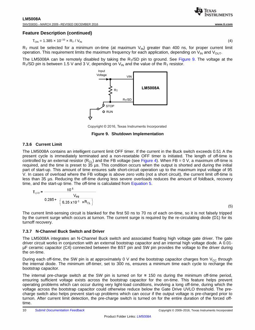
The LM5008A can be remotely disabled by taking the RT/SD pin to ground. See Figure 9. The voltage at theRT/SD pin is between 1.5 V and 3 V, depending on VIN and the value of the RT resistor.
Figure 9. Shutdown Implementation
7.3.6 Current LimitThe LM5008A contains an intelligent current limit OFF timer. If the current in the Buck switch exceeds 0.51 A thepresent cycle is immediately terminated and a non-resetable OFF timer is initiated. The length of off-time iscontrolled by an external resistor (RCL) and the FB voltage (see Figure 4). When FB = 0 V, a maximum off-time isrequired, and the time is preset to 35 µs. This condition occurs when the output is shorted and during the initialpart of start-up. This amount of time ensures safe short-circuit operation up to the maximum input voltage of 95V. In cases of overload where the FB voltage is above zero volts (not a short circuit), the current limit off-time isless than 35 µs. Reducing the off-time during less severe overloads reduces the amount of foldback, recoverytime, and the start-up time. The off-time is calculated from Equation 5.
(5)
The current limit-sensing circuit is blanked for the first 50 ns to 70 ns of each on-time, so it is not falsely trippedby the current surge which occurs at turnon. The current surge is required by the re-circulating diode (D1) for itsturnoff recovery.
7.3.7 N-Channel Buck Switch and DriverThe LM5008A integrates an N-Channel Buck switch and associated floating high voltage gate driver. The gatedriver circuit works in conjunction with an external bootstrap capacitor and an internal high voltage diode. A 0.01-µF ceramic capacitor (C4) connected between the BST pin and SW pin provides the voltage to the driver duringthe on-time.
During each off-time, the SW pin is at approximately 0 V and the bootstrap capacitor charges from VCC throughthe internal diode. The minimum off-timer, set to 300 ns, ensures a minimum time each cycle to recharge thebootstrap capacitor.
The internal pre-charge switch at the SW pin is turned on for ≊ 150 ns during the minimum off-time period,ensuring sufficient voltage exists across the bootstrap capacitor for the on-time. This feature helps preventoperating problems which can occur during very light-load conditions, involving a long off-time, during which thevoltage across the bootstrap capacitor could otherwise reduce below the Gate Drive UVLO threshold. The pre-charge switch also helps prevent start-up problems which can occur if the output voltage is pre-charged prior toturnon. After current limit detection, the pre-charge switch is turned on for the entire duration of the forced off-time.
� �OUTLBOUNDARY
F SW
V 1 DII
2 2 L F
� �'
� �
11
LM5008Awww.ti.com SNVS583G –MARCH 2009–REVISED DECEMBER 2016
Product Folder Links: LM5008A
Submit Documentation FeedbackCopyright © 2009–2016, Texas Instruments Incorporated
Feature Description (continued)7.3.8 Thermal ProtectionThe LM5008A must be operated so the junction temperature does not exceed 125°C during normal operation. Aninternal Thermal Shutdown circuit is provided to shutdown the LM5008A in the event of a higher than normaljunction temperature. When activated, typically at 165°C, the controller is forced into a low-power reset state bydisabling the buck switch. This feature prevents catastrophic failures from accidental device overheating. Whenthe junction temperature reduces below 140°C (typical hysteresis = 25°C), normal operation is resumed.
7.4 Device Functional Modes
7.4.1 Shutdown ModeThe RT/SD pin provides ON and OFF control for the LM5008A. When VSD is below approximately 0.7 V, thedevice is in shutdown mode. Both the internal LDO and the switching regulator are off. The quiescent current inshutdown mode drops to 110 µA (typical) at VIN = 48 V. The LM5008A also employs VCC bias rail undervoltageprotection. If the VCC bias supply voltage is below its UV threshold, the regulator remains off.
7.4.2 Active ModeLM5008A is in active mode when the internal bias rail, VCC, is above its UV threshold. Depending on the loadcurrent, the device operates in either DCM or CCM mode.
Whenever the load current is reduced to a level less than half the peak-to-peak inductor ripple current, the deviceenters discontinuous conduction mode (DCM). Calculate the critical conduction boundary using Equation 6.
(6)
When the inductor current reaches zero, the SW node becomes high impedance. Resonant ringing occurs at SWas a result of the LC tank circuit formed by the buck inductor and the parasitic capacitance at the SW node. Atlight loads, several pulses may be skipped in between switching cycles, effectively reducing the switchingfrequency and further improving light-load efficiency.
Copyright © 2016, Texas Instruments Incorporated
FB
VIN
SW
RTN
BST
LM5008A
8
6
5
3
4
1
2
7
SHUTDOWN
VCC
RCL
RT/SD
12 - 95V
Input
324k
C1
1.0 µF
RT
RCL
332kRFB1
1.0k
RFB2
3.01k
R33.0
GND
C2
22 µF
VOUT
10.0V
L1
220 PH
C3
0.47 µF
C4
0.01 µF
D1
C5
0.1 µF
12
LM5008ASNVS583G –MARCH 2009–REVISED DECEMBER 2016 www.ti.com
Product Folder Links: LM5008A
Submit Documentation Feedback Copyright © 2009–2016, Texas Instruments Incorporated
8 Application and Implementation
NOTEInformation in the following applications sections is not part of the TI componentspecification, and TI does not warrant its accuracy or completeness. TI’s customers areresponsible for determining suitability of components for their purposes. Customers shouldvalidate and test their design implementation to confirm system functionality.
8.1 Application InformationLM5008A requires only a few external components to convert from a wide range of supply voltages to a fixedoutput voltage. To expedite and streamline the process of designing a LM5008A-based converter, acomprehensive LM5008A Quick-Start tool is available for download to assist the designer with componentselection for a given application. WEBENCH® online software is also available to generate complete designs,leveraging iterative design procedures and access to comprehensive component databases. The followingsections discuss a design procedure using a typical application example. The application circuit detailed belowshows the LM5008A in a configuration suitable for several application use cases. See the LM5008A EVM formore details.
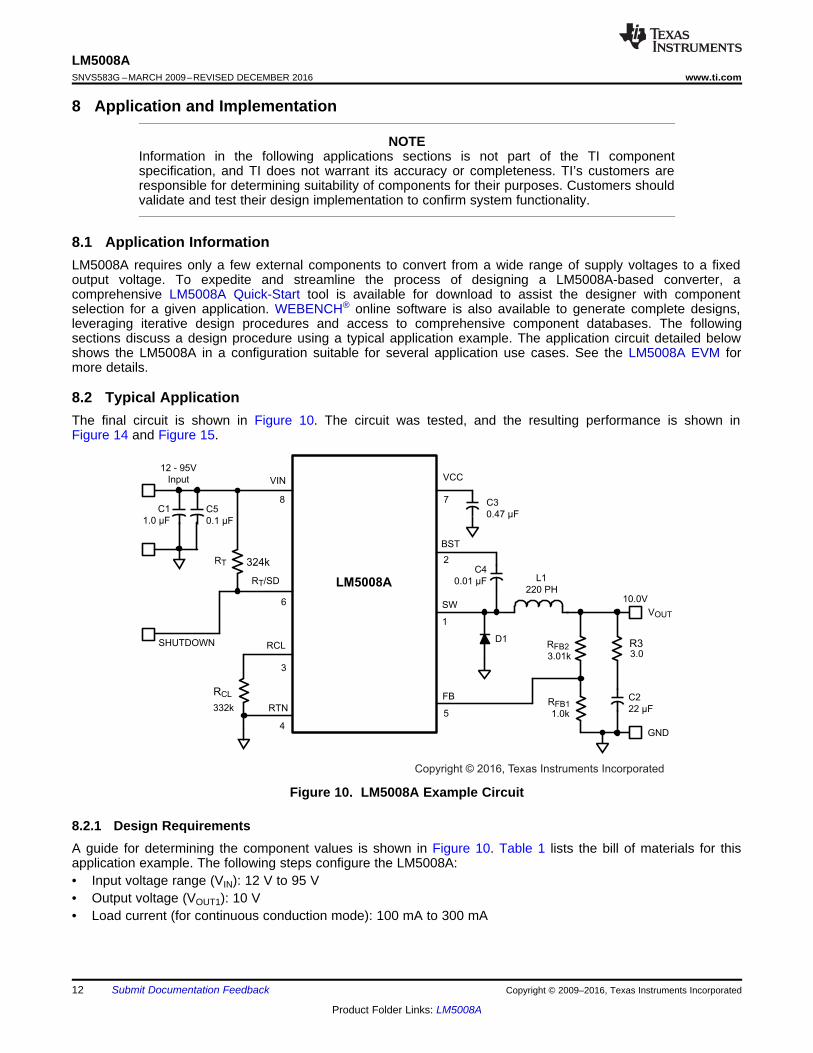
8.2 Typical ApplicationThe final circuit is shown in Figure 10. The circuit was tested, and the resulting performance is shown inFigure 14 and Figure 15.
Figure 10. LM5008A Example Circuit
8.2.1 Design RequirementsA guide for determining the component values is shown in Figure 10. Table 1 lists the bill of materials for thisapplication example. The following steps configure the LM5008A:• Input voltage range (VIN): 12 V to 95 V• Output voltage (VOUT1): 10 V• Load current (for continuous conduction mode): 100 mA to 300 mA
OUT IN OUT
OR s IN
V (V V )L1=
I F V
u �
u u
13
LM5008Awww.ti.com SNVS583G –MARCH 2009–REVISED DECEMBER 2016
Product Folder Links: LM5008A
Submit Documentation FeedbackCopyright © 2009–2016, Texas Instruments Incorporated
Typical Application (continued)Table 1. Bill of Materials
ITEM DESCRIPTION PART NUMBER VALUEC1 Ceramic Capacitor TDK C4532X7R2A105M 1 µF, 100 VC2 Ceramic Capacitor TDK C4532X7R1E226M 22 µF, 25 VC3 Ceramic Capacitor Kemet C1206C474K5RAC 0.47 µF, 50 VC4 Ceramic Capacitor Kemet C1206C103K5RAC 0.01 µF, 50 VC5 Ceramic Capacitor TDK C3216X7R2A104M 0.1 µF, 100 VD1 Schottky Power Diode Diodes Inc. DFLS1100 100 V, 1 A
L1 Power Inductor COILTRONICS DR125-221-R orTDK SLF10145T-221MR65 220 µH
RFB2 Resistor Vishay CRCW12063011F 3.01 kΩRFB1 Resistor Vishay CRCW12061001F 1.0 kΩR3 Resistor Vishay CRCW12063R00F 3.0 Ω
RT Resistor Vishay CRCW12063243F 324 kΩRCL Resistor Vishay CRCW12063323F 332 kΩU1 Switching Regulator LM5008A
8.2.2 Detailed Design Procedure
8.2.2.1 Selection Of External ComponentsRFB1, RFB2: VOUT = VFB × (RFB1 + RFB2) / RFB1, and because VFB = 2.5 V, the ratio of RFB2 to RFB1 calculates as3:1. Standard values of 3.01 kΩ and 1 kΩ are chosen. Other values could be used as long as the 3:1 ratio ismaintained.
Fs and RT: The recommended operating frequency range for the LM5008A is 50 kHz to 1.1 MHz. Unless theapplication requires a specific frequency, the choice of frequency is generally a compromise because it affectsthe size of L1 and C2 and the switching losses. The maximum allowed frequency, based on a minimum on-timeof 400 ns, is calculated with Equation 7.
FMAX = VOUT / (VINMAX × 400 ns) (7)
For this exercise, FMAX = 263 kHz. From Equation 2, RT calculates to 274 kΩ. A standard value 324-kΩ resistor isused to allow for tolerances in Equation 2, resulting in a frequency of 223 kHz.
L1: The main parameter affected by the inductor is the output current ripple amplitude. The choice of inductorvalue therefore depends on both the minimum and maximum load currents, keeping in mind that the maximumripple current occurs at maximum VIN.a. Minimum load current: To maintain continuous conduction at minimum Io (100 mA), the ripple amplitude
(IOR) must be less than 200 mAp-p so the lower peak of the waveform does not reach zero. L1 is calculatedusing Equation 8.
(8)
At VIN = 95 V, L1 (minimum) calculates to 200 µH. The next larger standard value (220 µH) is chosen andwith this value IOR calculates to 182 mAp-p at VIN = 95 V, and 34 mAp-p at VIN = 12 V.
b. Maximum load current: At a load current of 300 mA, the peak of the ripple waveform must not reach theminimum value of the LM5008A’s current limit threshold (410 mA). Therefore the ripple amplitude must beless than 220 mAp-p, which is already satisfied in Equation 8. With L1 = 220 µH, at maximum VIN and IO, thepeak of the ripple is 391 mA. While L1 must carry this peak current without saturating or exceeding itstemperature rating, it also must be capable of carrying the maximum value of the LM5008A’s current limitthreshold (610 mA) without saturating because the current limit is reached during start-up.The DC resistance of the inductor must be as low as possible. For example, if the inductor’s DCR is 1 Ω, thepower dissipated at maximum load current is 0.09 W. While small, it is not insignificant compared to the loadpower of 3 W.
ONI t 0.3A 3.74 SC1 0.56 F
V 2.0V
u u P P
'
14
LM5008ASNVS583G –MARCH 2009–REVISED DECEMBER 2016 www.ti.com
Product Folder Links: LM5008A
Submit Documentation Feedback Copyright © 2009–2016, Texas Instruments Incorporated
C3: The capacitor on the VCC output provides not only noise filtering and stability, but its primary purpose is toprevent false triggering of the VCC UVLO at the buck switch on and off transitions. C3 must be no smaller than0.47 µF.
C2, and R3: When selecting the output filter capacitor C2, the items to consider are ripple voltage due to itsESR, ripple voltage due to its capacitance, and the nature of the load.
ESR and R3: A low ESR for C2 is generally desirable to minimize power losses and heating within the capacitor.However, the regulator requires a minimum amount of ripple voltage at the feedback input for proper loopoperation. For the LM5008A the minimum ripple required at pin 5 is 25 mVp-p, requiring a minimum ripple atVOUT of 100 mV. Because the minimum ripple current (at minimum VIN) is 34 mA p-p, the minimum ESR requiredat VOUT is 100 mV / 34 mA = 2.94 Ω. Because quality capacitors for SMPS applications have an ESRconsiderably less than this, R3 is inserted as shown in the Functional Block Diagram. R3’s value, along with C2’sESR, must result in at least 25 mVp-p ripple at pin 5. Generally, R3 is 0.5 to 3 Ω.
RCL: When current limit is detected, the minimum off-time set by this resistor must be greater than the maximumnormal off-time, which occurs at maximum input voltage. Using Equation 4, the minimum on-time is 472 ns,yielding an off-time of 4 µs (at 223 kHz). Due to the 25% tolerance on the on-time, the off-time tolerance is also25%, yielding a maximum off-time of 5 µs. Allowing for the response time of the current limit detection circuit(350 ns) increases the maximum off-time to 5.35 µs. This is increased an additional 25% to 6.7 µs to allow forthe tolerances of Equation 5. Using Equation 5, RCL calculates to 325 kΩ at VFB = 2.5 V. A standard value 332-kΩ resistor is used.
D1: The important parameters are reverse recovery time and forward voltage. The reverse recovery timedetermines how long the reverse current surge lasts each time the buck switch is turned on. The forward voltagedrop is significant in the event the output is short-circuited as it is only this diode’s voltage which forces theinductor current to reduce during the forced off-time. For this reason, a higher voltage is better, although thataffects efficiency. A good choice is a Schottky power diode, such as the DFLS1100. D1’s reverse voltage ratingmust be at least as great as the maximum VIN, and its current rating be greater than the maximum current limitthreshold (610 mA).
C1: This capacitor’s purpose is to supply most of the switch current during the on-time, and limit the voltageripple at VIN, on the assumption that the voltage source feeding VIN has an output impedance greater than zero.At maximum load current, when the buck switch turns on, the current into pin 8 suddenly increases to the lowerpeak of the output current waveform, ramp up to the peak value, then drop to zero at turnoff. The average inputcurrent during this on-time is the load current (300 mA). For a worst-case calculation, C1 must supply thisaverage load current during the maximum on-time. To keep the input voltage ripple to less than 2 V (for thisexercise), C1 is calculated with Equation 9.
(9)
Quality ceramic capacitors in this value have a low ESR which adds only a few millivolts to the ripple. It is thecapacitance which is dominant in this case. To allow for the capacitor’s tolerance, temperature effects, andvoltage effects, a 1-µF, 100-V, X7R capacitor is used.
C4: The recommended value is 0.01 µF for C4, as this is appropriate in the majority of applications. A high-quality ceramic capacitor with low ESR is recommended as C4 supplies the surge current to charge the buckswitch gate at turnon. A low ESR also ensures a quick recharge during each off-time. At minimum VIN, when theon-time is at maximum, it is possible during start-up that C4 does not fully recharge during each 300-ns off-time.The circuit is not able to complete the start-up, and achieve output regulation. This can occur when the frequencyis intended to be low (for example, RT = 500 K). In this case C4 must be increased so it can maintain sufficientvoltage across the buck switch driver during each on-time.
C5: This capacitor helps avoid supply voltage transients and ringing due to long lead inductance at VIN. A low-ESR, 0.1-µF ceramic chip capacitor is recommended placed close to the LM5008A.
Copyright © 2016, Texas Instruments Incorporated
SW
FB
LM5008A
L1
C2
CB
CARA
VOUT
RFB2
RFB1
Copyright © 2016, Texas Instruments Incorporated
FB
SW
L1
LM5008A Cff RFB2 R3
C2
VOUT
RFB1
ON(max)
FB1 FB2
3 tCff =
(R //R )
u
15
LM5008Awww.ti.com SNVS583G –MARCH 2009–REVISED DECEMBER 2016
Product Folder Links: LM5008A
Submit Documentation FeedbackCopyright © 2009–2016, Texas Instruments Incorporated
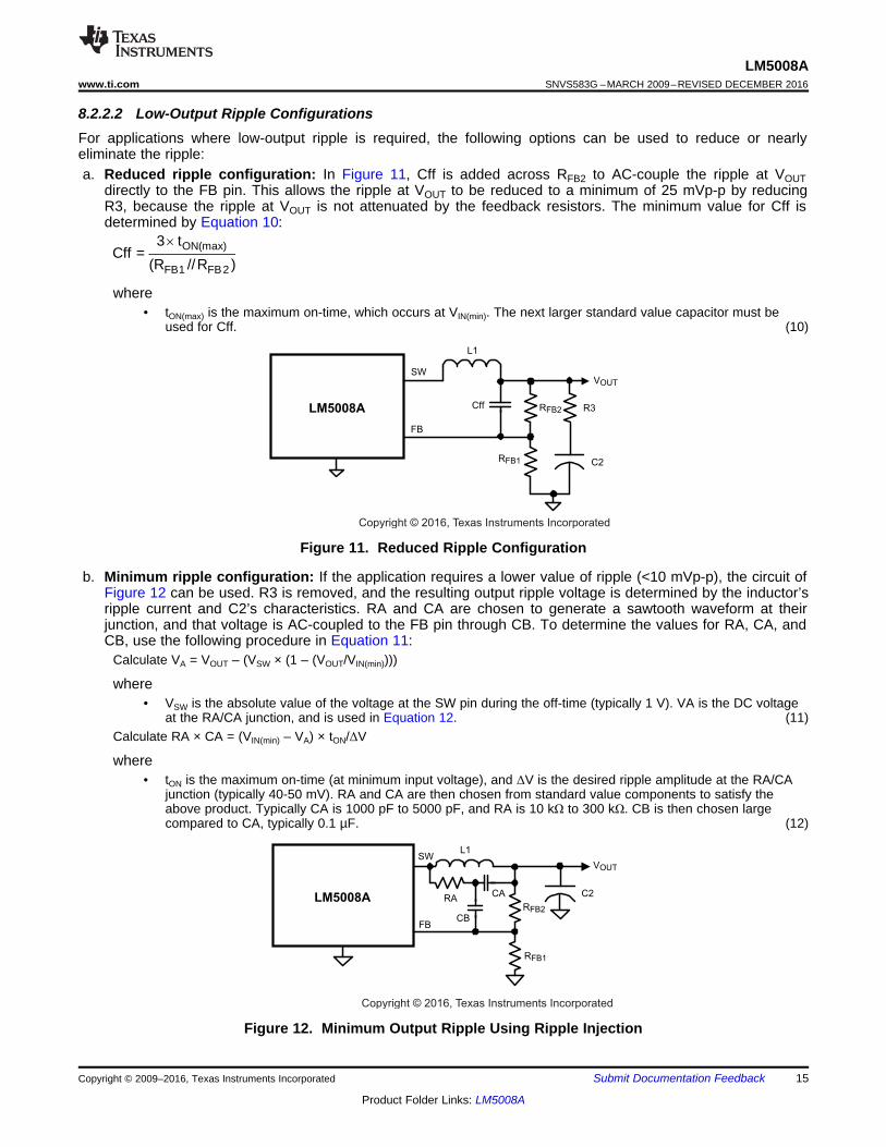
8.2.2.2 Low-Output Ripple ConfigurationsFor applications where low-output ripple is required, the following options can be used to reduce or nearlyeliminate the ripple:a. Reduced ripple configuration: In Figure 11, Cff is added across RFB2 to AC-couple the ripple at VOUT
directly to the FB pin. This allows the ripple at VOUT to be reduced to a minimum of 25 mVp-p by reducingR3, because the ripple at VOUT is not attenuated by the feedback resistors. The minimum value for Cff isdetermined by Equation 10:
where• tON(max) is the maximum on-time, which occurs at VIN(min). The next larger standard value capacitor must be
used for Cff. (10)
Figure 11. Reduced Ripple Configuration
b. Minimum ripple configuration: If the application requires a lower value of ripple (<10 mVp-p), the circuit ofFigure 12 can be used. R3 is removed, and the resulting output ripple voltage is determined by the inductor’sripple current and C2’s characteristics. RA and CA are chosen to generate a sawtooth waveform at theirjunction, and that voltage is AC-coupled to the FB pin through CB. To determine the values for RA, CA, andCB, use the following procedure in Equation 11:
Calculate VA = VOUT – (VSW × (1 – (VOUT/VIN(min))))
where• VSW is the absolute value of the voltage at the SW pin during the off-time (typically 1 V). VA is the DC voltage
at the RA/CA junction, and is used in Equation 12. (11)Calculate RA × CA = (VIN(min) – VA) × tON/ΔV
where• tON is the maximum on-time (at minimum input voltage), and ΔV is the desired ripple amplitude at the RA/CA
junction (typically 40-50 mV). RA and CA are then chosen from standard value components to satisfy theabove product. Typically CA is 1000 pF to 5000 pF, and RA is 10 kΩ to 300 kΩ. CB is then chosen largecompared to CA, typically 0.1 µF. (12)
Figure 12. Minimum Output Ripple Using Ripple Injection
K�
�
IN
OUTOUTIN V
IVI
Copyright © 2016, Texas Instruments Incorporated
FB
SW
L1
LM5008AR3
C2
VOUT
RFB2
RFB1
16
LM5008ASNVS583G –MARCH 2009–REVISED DECEMBER 2016 www.ti.com
Product Folder Links: LM5008A
Submit Documentation Feedback Copyright © 2009–2016, Texas Instruments Incorporated
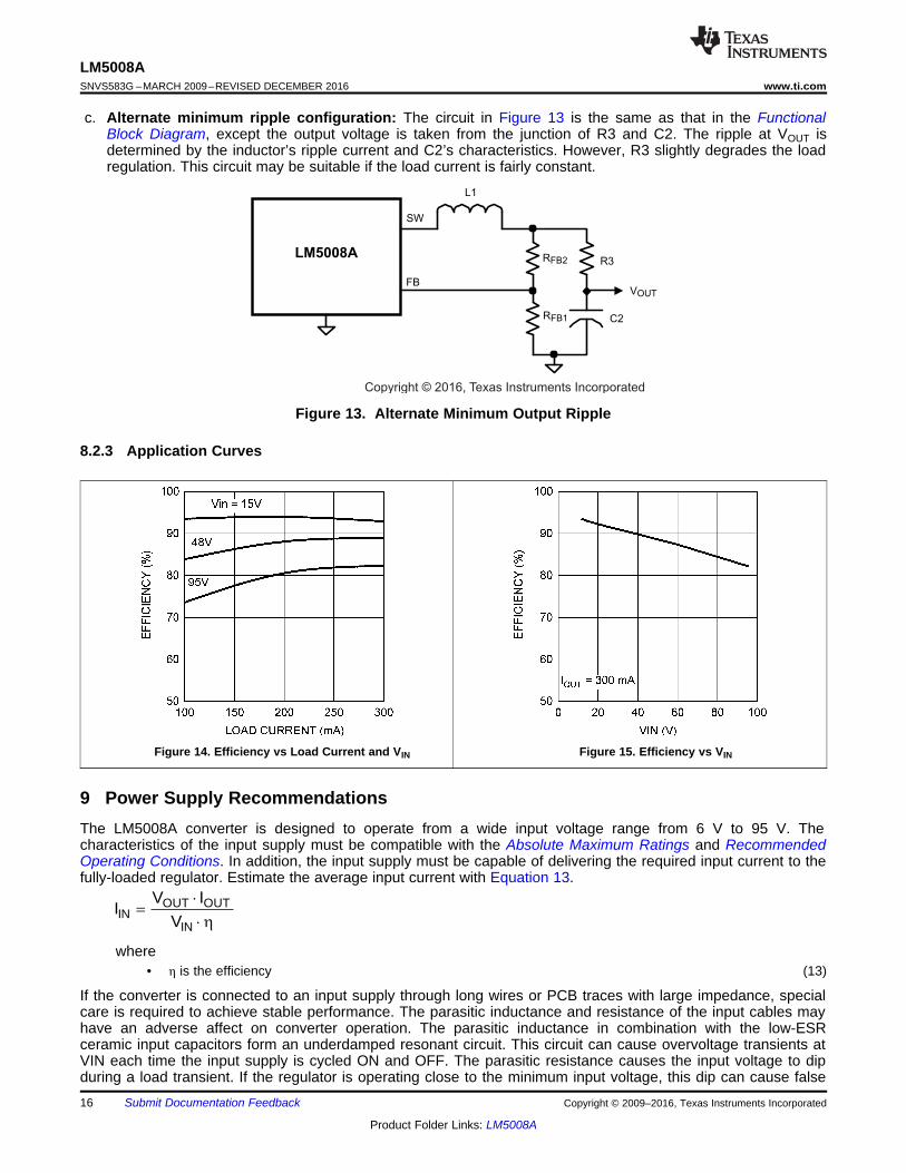
c. Alternate minimum ripple configuration: The circuit in Figure 13 is the same as that in the FunctionalBlock Diagram, except the output voltage is taken from the junction of R3 and C2. The ripple at VOUT isdetermined by the inductor’s ripple current and C2’s characteristics. However, R3 slightly degrades the loadregulation. This circuit may be suitable if the load current is fairly constant.
Figure 13. Alternate Minimum Output Ripple
8.2.3 Application Curves
Figure 14. Efficiency vs Load Current and VIN Figure 15. Efficiency vs VIN
9 Power Supply RecommendationsThe LM5008A converter is designed to operate from a wide input voltage range from 6 V to 95 V. Thecharacteristics of the input supply must be compatible with the Absolute Maximum Ratings and RecommendedOperating Conditions. In addition, the input supply must be capable of delivering the required input current to thefully-loaded regulator. Estimate the average input current with Equation 13.
where• η is the efficiency (13)
If the converter is connected to an input supply through long wires or PCB traces with large impedance, specialcare is required to achieve stable performance. The parasitic inductance and resistance of the input cables mayhave an adverse affect on converter operation. The parasitic inductance in combination with the low-ESRceramic input capacitors form an underdamped resonant circuit. This circuit can cause overvoltage transients atVIN each time the input supply is cycled ON and OFF. The parasitic resistance causes the input voltage to dipduring a load transient. If the regulator is operating close to the minimum input voltage, this dip can cause false
17
LM5008Awww.ti.com SNVS583G –MARCH 2009–REVISED DECEMBER 2016
Product Folder Links: LM5008A
Submit Documentation FeedbackCopyright © 2009–2016, Texas Instruments Incorporated
UVLO fault triggering and a system reset. The best way to solve such issues is to reduce the distance from theinput supply to the regulator and use an aluminum or tantalum input capacitor in parallel with the ceramics. Themoderate ESR of the electrolytic capacitors helps to damp the input resonant circuit and reduce any voltageovershoots. A capacitance in the range of 10 µF to 47 µF is usually sufficient to provide input damping and helpsto hold the input voltage steady during large load transients.
An EMI input filter is often used in front of the regulator that, unless carefully designed, can lead to instability aswell as some of the effects mentioned above. The user's guide Simple Success Wth Conducted EMI for DC-DCConverters (SNVA489) provides helpful suggestions when designing an input filter for any switching regulator.
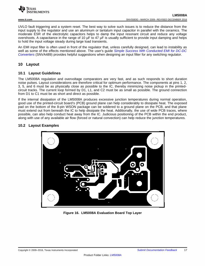
10 Layout
10.1 Layout GuidelinesThe LM5008A regulation and overvoltage comparators are very fast, and as such responds to short durationnoise pulses. Layout considerations are therefore critical for optimum performance. The components at pins 1, 2,3, 5, and 6 must be as physically close as possible to the IC, thereby minimizing noise pickup in the printed-circuit tracks. The current loop formed by D1, L1, and C2 must be as small as possible. The ground connectionfrom D1 to C1 must be as short and direct as possible.
If the internal dissipation of the LM5008A produces excessive junction temperatures during normal operation,good use of the printed-circuit board’s (PCB) ground plane can help considerably to dissipate heat. The exposedpad on the bottom of the 8-pin WSON package can be soldered to a ground plane on the PCB, and that planemust extend out from beneath the IC to help dissipate the heat. Additionally, the use of wide PCB traces, wherepossible, can also help conduct heat away from the IC. Judicious positioning of the PCB within the end product,along with use of any available air flow (forced or natural convection) can help reduce the junction temperatures.
10.2 Layout Examples
Figure 16. LM5008A Evaluation Board Top Layer
18
LM5008ASNVS583G –MARCH 2009–REVISED DECEMBER 2016 www.ti.com
Product Folder Links: LM5008A
Submit Documentation Feedback Copyright © 2009–2016, Texas Instruments Incorporated
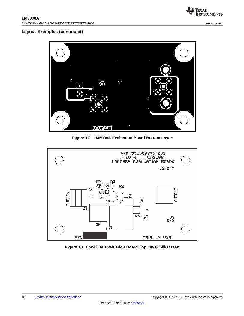
Layout Examples (continued)
Figure 17. LM5008A Evaluation Board Bottom Layer
Figure 18. LM5008A Evaluation Board Top Layer Silkscreen
19
LM5008Awww.ti.com SNVS583G –MARCH 2009–REVISED DECEMBER 2016
Product Folder Links: LM5008A
Submit Documentation FeedbackCopyright © 2009–2016, Texas Instruments Incorporated
11 Device and Documentation Support
11.1 Device Support
11.1.1 Development SupportFor development support see the following:• For TI's reference design library, visit TI Designs• For TI's WEBENCH Design Environments, visit WEBENCH® Design Center• For selecting components in LM5008A applications, see the LM5008A Quick-Start Calculator
11.2 Documentation Support
11.2.1 Related DocumentationFor related documentation see the following:• AN-1925 LM5008A Evaluation Board (SNVA380)• Buck Regulator Topologies for Wide Input/Output Voltage Differentials (SNVA594)
11.2.1.1 PCB Layout Resources• AN-1149 Layout Guidelines for Switching Power Supplies (SNVA021)• AN-1229 Simple Switcher PCB Layout Guidelines (SNVA054)• Constructing Your Power Supply – Layout Considerations (SLUP230)• Low Radiated EMI Layout Made SIMPLE with LM4360x and LM4600x (SNVA721)• AN-2162 Simple Success With Conducted EMI From DC-DC Converters (SNVA489)• Reduce Buck-Converter EMI and Voltage Stress by Minimizing Inductive Parasitics (SLYT682)
11.2.1.2 Thermal Design Resources• AN-2020 Thermal Design By Insight, Not Hindsight (SNVA419)• AN-1520 A Guide to Board Layout for Best Thermal Resistance for Exposed Pad Packages (SNVA183)• Semiconductor and IC Package Thermal Metrics (SPRA953)• Thermal Design Made Simple with LM43603 and LM43602 (SNVA719)• PowerPAD™Thermally Enhanced Package (SLMA002)• PowerPAD Made Easy (SLMA004)• Using New Thermal Metrics (SBVA025)
11.3 Receiving Notification of Documentation UpdatesTo receive notification of documentation updates, navigate to the device product folder on ti.com. In the upperright corner, click on Alert me to register and receive a weekly digest of any product information that haschanged. For change details, review the revision history included in any revised document.
11.4 Community ResourcesThe following links connect to TI community resources. Linked contents are provided "AS IS" by the respectivecontributors. They do not constitute TI specifications and do not necessarily reflect TI's views; see TI's Terms ofUse.
TI E2E™ Online Community TI's Engineer-to-Engineer (E2E) Community. Created to foster collaborationamong engineers. At e2e.ti.com, you can ask questions, share knowledge, explore ideas and helpsolve problems with fellow engineers.
Design Support TI's Design Support Quickly find helpful E2E forums along with design support tools andcontact information for technical support.
20
LM5008ASNVS583G –MARCH 2009–REVISED DECEMBER 2016 www.ti.com
Product Folder Links: LM5008A
Submit Documentation Feedback Copyright © 2009–2016, Texas Instruments Incorporated
11.5 TrademarksPowerPAD, E2E are trademarks of Texas Instruments.WEBENCH is a registered trademark of Texas Instruments.All other trademarks are the property of their respective owners.
11.6 Electrostatic Discharge CautionThese devices have limited built-in ESD protection. The leads should be shorted together or the device placed in conductive foamduring storage or handling to prevent electrostatic damage to the MOS gates.
11.7 GlossarySLYZ022 — TI Glossary.
This glossary lists and explains terms, acronyms, and definitions.
12 Mechanical, Packaging, and Orderable InformationThe following pages include mechanical, packaging, and orderable information. This information is the mostcurrent data available for the designated devices. This data is subject to change without notice and revision ofthis document. For browser-based versions of this data sheet, refer to the left-hand navigation.
PACKAGE OPTION ADDENDUM
www.ti.com 23-Feb-2016
Addendum-Page 1
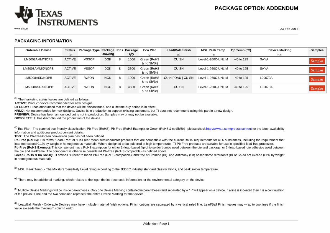
PACKAGING INFORMATION
Orderable Device Status(1)
Package Type PackageDrawing
Pins PackageQty
Eco Plan(2)
Lead/Ball Finish(6)
MSL Peak Temp(3)
Op Temp (°C) Device Marking(4/5)
Samples
LM5008AMM/NOPB ACTIVE VSSOP DGK 8 1000 Green (RoHS& no Sb/Br)
CU SN Level-1-260C-UNLIM -40 to 125 SAYA
LM5008AMMX/NOPB ACTIVE VSSOP DGK 8 3500 Green (RoHS& no Sb/Br)
CU SN Level-1-260C-UNLIM -40 to 125 SAYA
LM5008ASD/NOPB ACTIVE WSON NGU 8 1000 Green (RoHS& no Sb/Br)
CU NIPDAU | CU SN Level-1-260C-UNLIM -40 to 125 L00070A
LM5008ASDX/NOPB ACTIVE WSON NGU 8 4500 Green (RoHS& no Sb/Br)
CU SN Level-1-260C-UNLIM -40 to 125 L00070A
(1) The marketing status values are defined as follows:ACTIVE: Product device recommended for new designs.LIFEBUY: TI has announced that the device will be discontinued, and a lifetime-buy period is in effect.NRND: Not recommended for new designs. Device is in production to support existing customers, but TI does not recommend using this part in a new design.PREVIEW: Device has been announced but is not in production. Samples may or may not be available.OBSOLETE: TI has discontinued the production of the device.
(2) Eco Plan - The planned eco-friendly classification: Pb-Free (RoHS), Pb-Free (RoHS Exempt), or Green (RoHS & no Sb/Br) - please check http://www.ti.com/productcontent for the latest availabilityinformation and additional product content details.TBD: The Pb-Free/Green conversion plan has not been defined.Pb-Free (RoHS): TI's terms "Lead-Free" or "Pb-Free" mean semiconductor products that are compatible with the current RoHS requirements for all 6 substances, including the requirement thatlead not exceed 0.1% by weight in homogeneous materials. Where designed to be soldered at high temperatures, TI Pb-Free products are suitable for use in specified lead-free processes.Pb-Free (RoHS Exempt): This component has a RoHS exemption for either 1) lead-based flip-chip solder bumps used between the die and package, or 2) lead-based die adhesive used betweenthe die and leadframe. The component is otherwise considered Pb-Free (RoHS compatible) as defined above.Green (RoHS & no Sb/Br): TI defines "Green" to mean Pb-Free (RoHS compatible), and free of Bromine (Br) and Antimony (Sb) based flame retardants (Br or Sb do not exceed 0.1% by weightin homogeneous material)
(3) MSL, Peak Temp. - The Moisture Sensitivity Level rating according to the JEDEC industry standard classifications, and peak solder temperature.
(4) There may be additional marking, which relates to the logo, the lot trace code information, or the environmental category on the device.
(5) Multiple Device Markings will be inside parentheses. Only one Device Marking contained in parentheses and separated by a "~" will appear on a device. If a line is indented then it is a continuationof the previous line and the two combined represent the entire Device Marking for that device.
(6) Lead/Ball Finish - Orderable Devices may have multiple material finish options. Finish options are separated by a vertical ruled line. Lead/Ball Finish values may wrap to two lines if the finishvalue exceeds the maximum column width.
PACKAGE OPTION ADDENDUM
www.ti.com 23-Feb-2016
Addendum-Page 2
Important Information and Disclaimer:The information provided on this page represents TI's knowledge and belief as of the date that it is provided. TI bases its knowledge and belief on informationprovided by third parties, and makes no representation or warranty as to the accuracy of such information. Efforts are underway to better integrate information from third parties. TI has taken andcontinues to take reasonable steps to provide representative and accurate information but may not have conducted destructive testing or chemical analysis on incoming materials and chemicals.TI and TI suppliers consider certain information to be proprietary, and thus CAS numbers and other limited information may not be available for release.
In no event shall TI's liability arising out of such information exceed the total purchase price of the TI part(s) at issue in this document sold by TI to Customer on an annual basis.
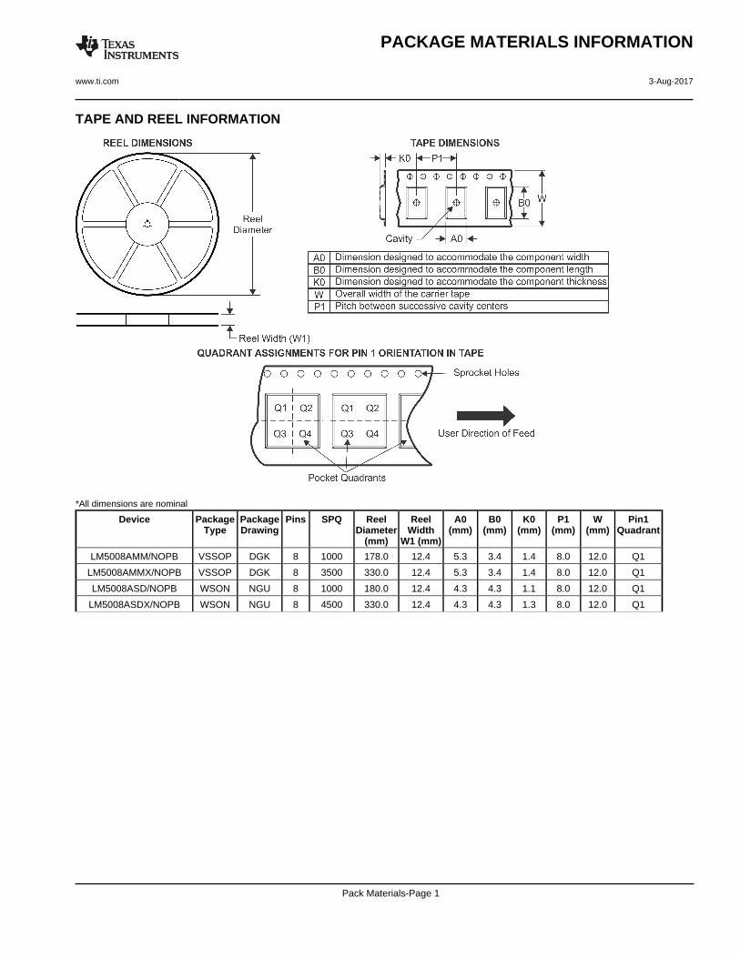
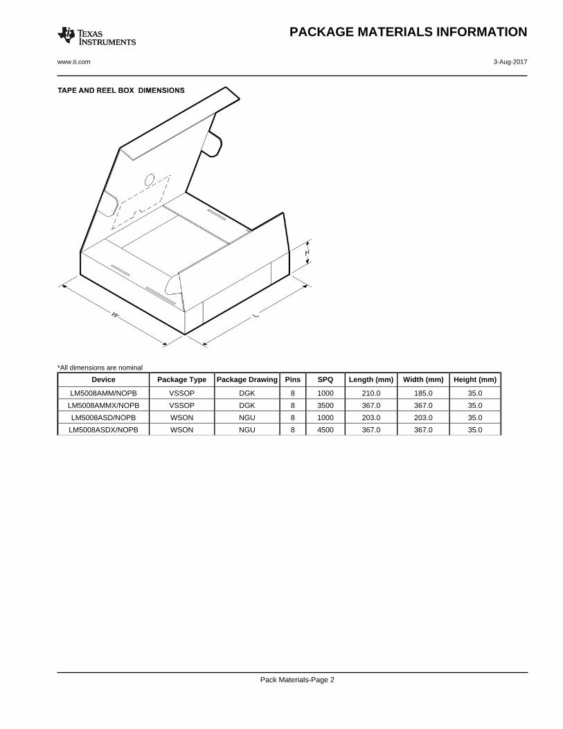
TAPE AND REEL INFORMATION
*All dimensions are nominal
Device PackageType
PackageDrawing
Pins SPQ ReelDiameter
(mm)
ReelWidth
W1 (mm)
A0(mm)
B0(mm)
K0(mm)
P1(mm)
W(mm)
Pin1Quadrant
LM5008AMM/NOPB VSSOP DGK 8 1000 178.0 12.4 5.3 3.4 1.4 8.0 12.0 Q1
LM5008AMMX/NOPB VSSOP DGK 8 3500 330.0 12.4 5.3 3.4 1.4 8.0 12.0 Q1
LM5008ASD/NOPB WSON NGU 8 1000 180.0 12.4 4.3 4.3 1.1 8.0 12.0 Q1
LM5008ASDX/NOPB WSON NGU 8 4500 330.0 12.4 4.3 4.3 1.3 8.0 12.0 Q1
PACKAGE MATERIALS INFORMATION
www.ti.com 3-Aug-2017
Pack Materials-Page 1
*All dimensions are nominal
Device Package Type Package Drawing Pins SPQ Length (mm) Width (mm) Height (mm)
LM5008AMM/NOPB VSSOP DGK 8 1000 210.0 185.0 35.0
LM5008AMMX/NOPB VSSOP DGK 8 3500 367.0 367.0 35.0
LM5008ASD/NOPB WSON NGU 8 1000 203.0 203.0 35.0
LM5008ASDX/NOPB WSON NGU 8 4500 367.0 367.0 35.0
PACKAGE MATERIALS INFORMATION
www.ti.com 3-Aug-2017
Pack Materials-Page 2
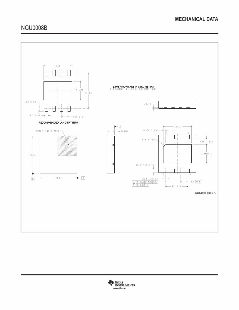
MECHANICAL DATA
NGU0008B
www.ti.com
SDC08B (Rev A)
IMPORTANT NOTICE
Texas Instruments Incorporated (TI) reserves the right to make corrections, enhancements, improvements and other changes to itssemiconductor products and services per JESD46, latest issue, and to discontinue any product or service per JESD48, latest issue. Buyersshould obtain the latest relevant information before placing orders and should verify that such information is current and complete.TI’s published terms of sale for semiconductor products (http://www.ti.com/sc/docs/stdterms.htm) apply to the sale of packaged integratedcircuit products that TI has qualified and released to market. Additional terms may apply to the use or sale of other types of TI products andservices.Reproduction of significant portions of TI information in TI data sheets is permissible only if reproduction is without alteration and isaccompanied by all associated warranties, conditions, limitations, and notices. TI is not responsible or liable for such reproduceddocumentation. Information of third parties may be subject to additional restrictions. Resale of TI products or services with statementsdifferent from or beyond the parameters stated by TI for that product or service voids all express and any implied warranties for theassociated TI product or service and is an unfair and deceptive business practice. TI is not responsible or liable for any such statements.Buyers and others who are developing systems that incorporate TI products (collectively, “Designers”) understand and agree that Designersremain responsible for using their independent analysis, evaluation and judgment in designing their applications and that Designers havefull and exclusive responsibility to assure the safety of Designers' applications and compliance of their applications (and of all TI productsused in or for Designers’ applications) with all applicable regulations, laws and other applicable requirements. Designer represents that, withrespect to their applications, Designer has all the necessary expertise to create and implement safeguards that (1) anticipate dangerousconsequences of failures, (2) monitor failures and their consequences, and (3) lessen the likelihood of failures that might cause harm andtake appropriate actions. Designer agrees that prior to using or distributing any applications that include TI products, Designer willthoroughly test such applications and the functionality of such TI products as used in such applications.TI’s provision of technical, application or other design advice, quality characterization, reliability data or other services or information,including, but not limited to, reference designs and materials relating to evaluation modules, (collectively, “TI Resources”) are intended toassist designers who are developing applications that incorporate TI products; by downloading, accessing or using TI Resources in anyway, Designer (individually or, if Designer is acting on behalf of a company, Designer’s company) agrees to use any particular TI Resourcesolely for this purpose and subject to the terms of this Notice.TI’s provision of TI Resources does not expand or otherwise alter TI’s applicable published warranties or warranty disclaimers for TIproducts, and no additional obligations or liabilities arise from TI providing such TI Resources. TI reserves the right to make corrections,enhancements, improvements and other changes to its TI Resources. TI has not conducted any testing other than that specificallydescribed in the published documentation for a particular TI Resource.Designer is authorized to use, copy and modify any individual TI Resource only in connection with the development of applications thatinclude the TI product(s) identified in such TI Resource. NO OTHER LICENSE, EXPRESS OR IMPLIED, BY ESTOPPEL OR OTHERWISETO ANY OTHER TI INTELLECTUAL PROPERTY RIGHT, AND NO LICENSE TO ANY TECHNOLOGY OR INTELLECTUAL PROPERTYRIGHT OF TI OR ANY THIRD PARTY IS GRANTED HEREIN, including but not limited to any patent right, copyright, mask work right, orother intellectual property right relating to any combination, machine, or process in which TI products or services are used. Informationregarding or referencing third-party products or services does not constitute a license to use such products or services, or a warranty orendorsement thereof. Use of TI Resources may require a license from a third party under the patents or other intellectual property of thethird party, or a license from TI under the patents or other intellectual property of TI.TI RESOURCES ARE PROVIDED “AS IS” AND WITH ALL FAULTS. TI DISCLAIMS ALL OTHER WARRANTIES ORREPRESENTATIONS, EXPRESS OR IMPLIED, REGARDING RESOURCES OR USE THEREOF, INCLUDING BUT NOT LIMITED TOACCURACY OR COMPLETENESS, TITLE, ANY EPIDEMIC FAILURE WARRANTY AND ANY IMPLIED WARRANTIES OFMERCHANTABILITY, FITNESS FOR A PARTICULAR PURPOSE, AND NON-INFRINGEMENT OF ANY THIRD PARTY INTELLECTUALPROPERTY RIGHTS. TI SHALL NOT BE LIABLE FOR AND SHALL NOT DEFEND OR INDEMNIFY DESIGNER AGAINST ANY CLAIM,INCLUDING BUT NOT LIMITED TO ANY INFRINGEMENT CLAIM THAT RELATES TO OR IS BASED ON ANY COMBINATION OFPRODUCTS EVEN IF DESCRIBED IN TI RESOURCES OR OTHERWISE. IN NO EVENT SHALL TI BE LIABLE FOR ANY ACTUAL,DIRECT, SPECIAL, COLLATERAL, INDIRECT, PUNITIVE, INCIDENTAL, CONSEQUENTIAL OR EXEMPLARY DAMAGES INCONNECTION WITH OR ARISING OUT OF TI RESOURCES OR USE THEREOF, AND REGARDLESS OF WHETHER TI HAS BEENADVISED OF THE POSSIBILITY OF SUCH DAMAGES.Unless TI has explicitly designated an individual product as meeting the requirements of a particular industry standard (e.g., ISO/TS 16949and ISO 26262), TI is not responsible for any failure to meet such industry standard requirements.Where TI specifically promotes products as facilitating functional safety or as compliant with industry functional safety standards, suchproducts are intended to help enable customers to design and create their own applications that meet applicable functional safety standardsand requirements. Using products in an application does not by itself establish any safety features in the application. Designers mustensure compliance with safety-related requirements and standards applicable to their applications. Designer may not use any TI products inlife-critical medical equipment unless authorized officers of the parties have executed a special contract specifically governing such use.Life-critical medical equipment is medical equipment where failure of such equipment would cause serious bodily injury or death (e.g., lifesupport, pacemakers, defibrillators, heart pumps, neurostimulators, and implantables). Such equipment includes, without limitation, allmedical devices identified by the U.S. Food and Drug Administration as Class III devices and equivalent classifications outside the U.S.TI may expressly designate certain products as completing a particular qualification (e.g., Q100, Military Grade, or Enhanced Product).Designers agree that it has the necessary expertise to select the product with the appropriate qualification designation for their applicationsand that proper product selection is at Designers’ own risk. Designers are solely responsible for compliance with all legal and regulatoryrequirements in connection with such selection.Designer will fully indemnify TI and its representatives against any damages, costs, losses, and/or liabilities arising out of Designer’s non-compliance with the terms and provisions of this Notice.
Mailing Address: Texas Instruments, Post Office Box 655303, Dallas, Texas 75265Copyright © 2017, Texas Instruments Incorporated