Embed Size (px)
Citation preview

1SNVA761–September 2016Submit Documentation Feedback
Copyright © 2016, Texas Instruments Incorporated
LM3481, LM3488, and LM3478 – How to Design Flyback Converter WithLM3481 Boost Controller
All trademarks are the property of their respective owners.
Application ReportSNVA761–September 2016
How to Design Flyback Converter With LM3481 BoostController
Vincent Zhang, Ambreesh Tripathi
ABSTRACTThe Texas Instruments LM3481 boost controller is a versatile low-side N-FET high-performance controllerfor switching regulators. The device has wide range of applications such as automotive start-stopapplication, one-cell or two-cell Li-ion battery-powered portable Bluetooth audio system, industrial systemisolated supplies, and so forth, and supports topologies like boost, SEPIC, and flyback. This applicationnote describes the design principles of the flyback converter with the circuit operation based on LM3481.
The report is broadly divided into three parts:1. Principle of flyback converter and features of LM34812. Step-by-step calculation followed by simulation (on Simplis)3. Test bench results
Contents1 LM3481 Description ......................................................................................................... 22 Principle of Flyback Converter ............................................................................................. 23 Flyback Parameters Design ................................................................................................ 44 LM3481 Flyback Parameters Design ..................................................................................... 95 Bench Verification .......................................................................................................... 166 Conclusion .................................................................................................................. 177 References .................................................................................................................. 17
List of Figures
1 LM3481 Pin Configuration .................................................................................................. 22 Topology of Flyback ......................................................................................................... 33 Flyback Main Waveform in CCM .......................................................................................... 44 LM3481 Functional Block Diagram........................................................................................ 75 The Overall Control Implementation ...................................................................................... 76 The Small Signal Model of CCM Flyback Converter.................................................................... 77 Control Block For Current Regulation Loop .............................................................................. 88 Typical LM431 Configuration With Output Bias and Optocoupler..................................................... 99 The Curve of Lm and Vin Relationship.................................................................................. 1010 LM3481-Flyback Schematic .............................................................................................. 1111 Calculated LM3481-Flyback Bode Plot – Gain-Frequency ........................................................... 1212 Calculated LM3481-Flyback Bode Plot – Phase-Frequency ......................................................... 1213 LM3481 Simplis Simulation Schematic.................................................................................. 1314 LM3481 Simplis Simulation Results ..................................................................................... 1415 Compensation Circuit Bode Plot Calculated Results – Gain-Frequency............................................ 1516 Compensation Circuit Bode Plot Calculated Results – Phase-Frequency.......................................... 1517 Compensation Simplis Simulation Results ............................................................................. 1518 LM3481 Flyback Bode Plot Calculated Results – Gain-Frequency.................................................. 16
LM3481
VINISEN
COMP
FB
AGND
UVLO VCC
DR
PGND
FA/SYNC/SD
1
2
3
4
5 6
7
8
9
10
LM3481 Description www.ti.com
2 SNVA761–September 2016Submit Documentation Feedback
Copyright © 2016, Texas Instruments Incorporated
LM3481, LM3488, and LM3478 – How to Design Flyback Converter WithLM3481 Boost Controller
19 LM3481 Flyback Bode Plot Calculated Results – Phase-Frequency................................................ 1620 LM3481 Flyback Bode Plot Simulation Results ........................................................................ 1621 Maximum Output Ripple at Different Input Voltage – VIN = 5.5 V.................................................... 1622 Maximum Output Ripple at Different Input Voltage – VIN = 28 V..................................................... 1623 Load Transient Response at 12 VIN .................................................................................... 1724 LM3481 Flyback EVM Bode Plot Tested Results ...................................................................... 17
List of Tables
1 The Meaning of PCM Overall Control Implementation Parameters................................................... 62 Design Specifications ....................................................................................................... 9
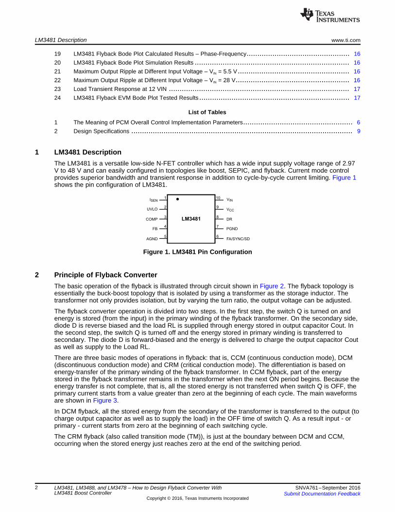
1 LM3481 DescriptionThe LM3481 is a versatile low-side N-FET controller which has a wide input supply voltage range of 2.97V to 48 V and can easily configured in topologies like boost, SEPIC, and flyback. Current mode controlprovides superior bandwidth and transient response in addition to cycle-by-cycle current limiting. Figure 1shows the pin configuration of LM3481.
Figure 1. LM3481 Pin Configuration
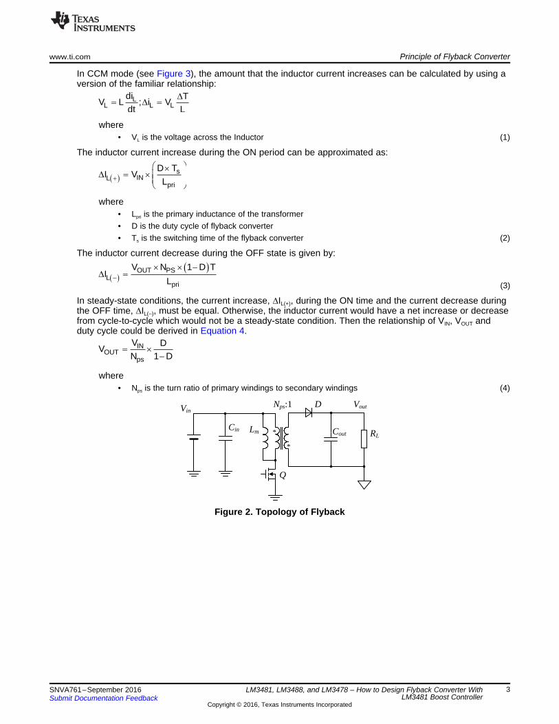
2 Principle of Flyback ConverterThe basic operation of the flyback is illustrated through circuit shown in Figure 2. The flyback topology isessentially the buck-boost topology that is isolated by using a transformer as the storage inductor. Thetransformer not only provides isolation, but by varying the turn ratio, the output voltage can be adjusted.
The flyback converter operation is divided into two steps. In the first step, the switch Q is turned on andenergy is stored (from the input) in the primary winding of the flyback transformer. On the secondary side,diode D is reverse biased and the load RL is supplied through energy stored in output capacitor Cout. Inthe second step, the switch Q is turned off and the energy stored in primary winding is transferred tosecondary. The diode D is forward-biased and the energy is delivered to charge the output capacitor Coutas well as supply to the Load RL.
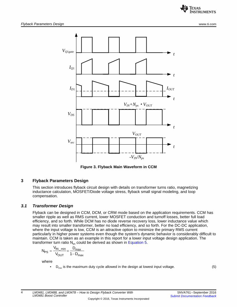
There are three basic modes of operations in flyback: that is, CCM (continuous conduction mode), DCM(discontinuous conduction mode) and CRM (critical conduction mode). The differentiation is based onenergy-transfer of the primary winding of the flyback transformer. In CCM flyback, part of the energystored in the flyback transformer remains in the transformer when the next ON period begins. Because theenergy transfer is not complete, that is, all the stored energy is not transferred when switch Q is OFF, theprimary current starts from a value greater than zero at the beginning of each cycle. The main waveformsare shown in Figure 3.
In DCM flyback, all the stored energy from the secondary of the transformer is transferred to the output (tocharge output capacitor as well as to supply the load) in the OFF time of switch Q. As a result input - orprimary - current starts from zero at the beginning of each switching cycle.
The CRM flyback (also called transition mode (TM)), is just at the boundary between DCM and CCM,occurring when the stored energy just reaches zero at the end of the switching period.
Vin
RL
*
*
Nps:1 Vout
Cin Cout
D
Q
Lm
INOUT
ps
V DV
N 1 D u
�
� �� �OUT PS
Lpri
V N 1 D TI
L�
u u �'
� �s
INLpri
D TI V
L�
§ ·u' u ¨ ¸¨ ¸
© ¹
LL L L
di TV L ; i V
dt L'
'
www.ti.com Principle of Flyback Converter
3SNVA761–September 2016Submit Documentation Feedback
Copyright © 2016, Texas Instruments Incorporated
LM3481, LM3488, and LM3478 – How to Design Flyback Converter WithLM3481 Boost Controller
In CCM mode (see Figure 3), the amount that the inductor current increases can be calculated by using aversion of the familiar relationship:
where• VL is the voltage across the Inductor (1)
The inductor current increase during the ON period can be approximated as:
where• Lpri is the primary inductance of the transformer• D is the duty cycle of flyback converter• Ts is the switching time of the flyback converter (2)
The inductor current decrease during the OFF state is given by:
(3)
In steady-state conditions, the current increase, ∆IL(+), during the ON time and the current decrease duringthe OFF time, ∆IL(–), must be equal. Otherwise, the inductor current would have a net increase or decreasefrom cycle-to-cycle which would not be a steady-state condition. Then the relationship of VIN, VOUT andduty cycle could be derived in Equation 4.
where• Nps is the turn ratio of primary windings to secondary windings (4)
Figure 2. Topology of Flyback
IN_min maxPS
OUT max
V DN
V 1 D u
�
VQ1gate
IQ1
ID1
VDS
Vsec
t
t
t
t
t
IOUT
VIN+Nps·VOUT
VOUT
-VIN/Nps
Flyback Parameters Design www.ti.com
4 SNVA761–September 2016Submit Documentation Feedback
Copyright © 2016, Texas Instruments Incorporated
LM3481, LM3488, and LM3478 – How to Design Flyback Converter WithLM3481 Boost Controller
Figure 3. Flyback Main Waveform in CCM
3 Flyback Parameters DesignThis section introduces flyback circuit design with details on transformer turns ratio, magnetizinginductance calculation, MOSFET/Diode voltage stress, flyback small signal modeling, and loopcompensation.
3.1 Transformer DesignFlyback can be designed in CCM, DCM, or CRM mode based on the application requirements. CCM hassmaller ripple as well as RMS current, lower MOSFET conduction and turnoff losses, better full loadefficiency, and so forth. While DCM has no diode reverse recovery loss, lower inductance value whichmay result into smaller transformer, better no load efficiency, and so forth. For the DC-DC application,where the input voltage is low, CCM is an attractive option to minimize the primary RMS currentparticularly in higher power systems even though the system's dynamic behavior is considerably difficult tomaintain. CCM is taken as an example in this report for a lower input voltage design application. Thetransformer turn ratio Nps could be derived as shown in Equation 5.
where• Dmax is the maximum duty cycle allowed in the design at lowest input voltage. (5)
� � � �
� �
ds _MOS IN_MAX OUT ps
IN_MAXR _ diode OUT
ps
V 1.5 ~ 2 V V N
VV 1.2 ~ 1.5 V
N
u � u
§ · u �¨ ¸¨ ¸
© ¹
� �O IN OUT psLpk _L
IN OUT ps
P V V NKI 1
2 V V N
u � u§ · � u¨ ¸ u uKu© ¹
� �
2 22OUT psIN
M IN 2L O S IN OUT ps
V NVL (V )
K P V V¦ N
uuK u
u u � u
IN LM OV I D Pu u uK
www.ti.com Flyback Parameters Design
5SNVA761–September 2016Submit Documentation Feedback
Copyright © 2016, Texas Instruments Incorporated
LM3481, LM3488, and LM3478 – How to Design Flyback Converter WithLM3481 Boost Controller
Suppose the efficiency of the flyback converter is η, the input power and output power relationship couldbe derived as shown in Equation 6.
where• ILM is the average current flowing in the transformer primary winding, which is also equals to the input
average current (6)
Setting the magnetizing inductor current as:ΔIL=KLILM
where• KL is the fraction chosen (7)
According to Equation 2, Equation 4, Equation 6, and Equation 7, LM function could be derived as shownin Equation 8.
where• PO is output power• fs is flyback converter frequency (8)
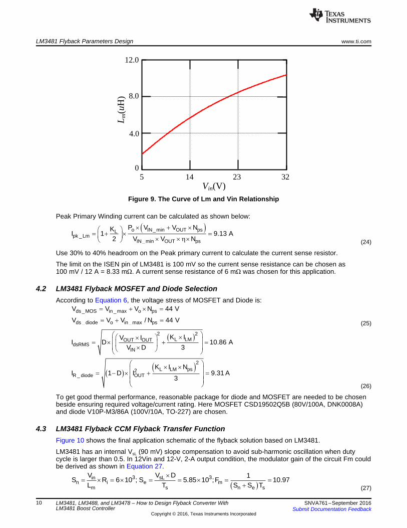
From this equation, it also could be observed that LM has positive correlation with VIN. That means themagnetizing inductor should be designed at highest input voltage to ensure the converter could run atCCM during all the input voltage range.
The peak current flowing in the primary winding can be calculated as:
(9)
The calculated turns ratio, primary winding inductance and peak current can be used to determine themagnetic core of the transformer, number of turns on primary and secondary windings, as well as wirethickness.
3.2 MOSFET and Diode SelectionAs shown in Figure 3, the voltage across the MOSFET during off time is VIN + VOUT × Nps and across thediode when it is reversed biased is VOUT + VIN / Nps. The voltage rating of the MOSFET and the diodeneeds to be chosen with appropriate margin as both of them suffers from high voltage spike. In case ofMOSFET, the primary leakage inductance resonates with output capacitance of MOSFET and similarly incase of diode, secondary leakage inductance resonates with diode capacitance and results into highvoltage spikes. Considering the spike voltage, usually choose 1.5~2 times of the voltage stage as thevoltage rating to ensure sufficient margin.
The voltage rating of MOSFET and Diode could be derived as shown in Equation 10.
(10)
The current RMS rating of MOSFET and Diode could be derived as shown in Equation 11.
� �� �
� �
ININ psLm
dim
VV D NÖi s 1 DH s
Ö L sd s
� u u� |
u
� � � �� �
IN INout IN ps
Lm Ldi 2
2IN mm out
OUT L
V V1sC V D N
Öi s 1 D R 1 DH s
Öd s V D Ls s L C
V R
§ ·u � u � u u¨ ¸� �© ¹ § ·u
� �¨ ¸© ¹
� � � � � � � �� �outOUT
ps Lm out outLd L
Öv sVÖ Ö Ö1 D N i s d s sC V s
R R� u u � u �
� � � � � � � � � �in IN ps OUT m Lm ps outÖ ÖÖ ÖD v s V N V d s sL i s N v su � � u u u � u
� �mn e s
1F
S S T
�
� �
� �� �
2 2L LMOUT OUT
dsRMSIN
2L LM ps2
R _ diode OUT
K IV II D
V D 3
K I NI 1 D I
3
§ ·u§ ·u¨ ¸ u �¨ ¸¨ ¸u© ¹© ¹
§ ·u u¨ ¸ � u �¨ ¸¨ ¸© ¹
Flyback Parameters Design www.ti.com
6 SNVA761–September 2016Submit Documentation Feedback
Copyright © 2016, Texas Instruments Incorporated
LM3481, LM3488, and LM3478 – How to Design Flyback Converter WithLM3481 Boost Controller
(11)
The current rating of MOSFET and Diode should at least be Ipk_LM and IOUT respectively.
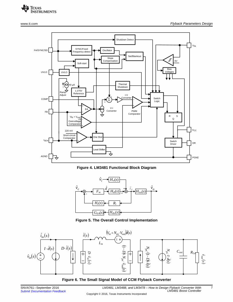
3.3 CCM Flyback Small Signal ModelingFigure 4 is LM3481 functional block diagram and Figure 5 is the Peak Current mode overall controlimplementation. The IL (inductor current) disturbance includes two parts: VIN and duty cycle, which isgenerated by the comparison of a current sampling RAMP and output of the EA (Error Amplifier). As thecurrent waveform is in conjunction with external ramp, the modulator gain of the circuit Fm is:
(12)
The meaning of PCM control implementation parameters are shown in Table 1.
Table 1. The Meaning of PCM Overall Control Implementation Parameters
Ts Switching period Hvoi(s) IL to output voltage transfer function
SnOn-time slope of the sensed-current
waveform HEA(s) Gain function of the error amplifier
Se External ramp Hdiv(s) Gain of the divided resistor networkRi Current sample resistor He(s) Sample-and-hold system gain function
Hdi(s) Duty cycle to IL transfer function Hvi(s) Input voltage to IL transfer function
Figure 6 is the average small signal model of flyback converter. According to the KCL and KVL principle,use Equation 13 and Equation 14:
(13)
(14)
To separate the small signal disturbance, the gain function from duty cycle to inductor current could becalculated as shown in Equation 15.
(15)
Considering the practical crossover frequency is much higher than the corner frequency with PCM control,simplify Equation 15 to Equation 16:
(16)
� �siinÖ
Lm
Cout
� �siÖ� � � �sdVNV outpsin
��
��s
voutÖRLd
� �svinÖ
� �sdI Ö� � �siD Ö�
����s
iD
Nps
Ö1
��
�
��s
dI
Nps
Ö�
�
��s
vD
inÖ�
��
��s
vN
Dout
psÖ
1�
��
LiÖ
ivÖ
cvÖ ovÖ
Hvi(s)
Hdi(s) Hivo(s)
RiHe(s)
dÖ
GEA(s) Hdiv(s)
Fm
FB
FA/SYNC/SD
COMP
ISEN
AGND PGND
DR
VIN
Shutdown Detect
SYNC/Fixed Frequency detect
Soft-start
+
EA+
-
+
Slope Compensation
Thermal Shutdown
Set/Blankout
SwitchLogic
SwitchDriver
1.275V Reference
Oscillator
+
220 mV
Level Shifter
6+
One Shot
Bias Voltages
6V
Overvoltage Comparator
Short-circuitComparator
Ramp Adjust
V-I Converter
I-V Converter
PWM Comparator
R SQ
VCC
UVLOUVLO
40 éA
Vfb + Vovp-
-
--
www.ti.com Flyback Parameters Design
7SNVA761–September 2016Submit Documentation Feedback
Copyright © 2016, Texas Instruments Incorporated
LM3481, LM3488, and LM3478 – How to Design Flyback Converter WithLM3481 Boost Controller
Figure 4. LM3481 Functional Block Diagram
Figure 5. The Overall Control Implementation
Figure 6. The Small Signal Model of CCM Flyback Converter
� �� �
� �� �
� �comp opto up 1 fb1 1 2 2
EAo opto fb1 1 2 up 2
Öv s K R R R C s 1 R C s 1H s
Öv s R R C s R R C s 1
� u u � u � � u
u ª º� u �¬ ¼
� �� �
� �
� �
� �comp opto up 1 fb1 1 2 2
EA 2o opto fb1 1 2 up 2 opto 2 up opto up 2 2
Öv s K R R R C s 1 R C s 1H s
Öv s R R C s R R C C s C R C R R C s 1
� u u � u � �
u u � � � u �
� �� �
� �
� � � �
� � � �o m di ivo
c e i m di
Öv s F H s H sPS s
Öv s 1 H s R F H s
u u
� u u u
� �� �
� �
� �
� � � �Lm di
c e i m di
Öi s F H sH s
Öv s 1 H s R F H s
u
� u u u
LmiÖ
Hdi(s)
RiHe(s)
dÖFm
cvÖ
� �S S
2S
e T 2
SS
T S s sH s 1
2e 1 TT
u
u | � �
� § ·S¨ ¸© ¹
� � � �� �
m OUTps
0 IN Livo
outLmps
L
L VN 1 s
Öv s V RH s
Ö s C 1 1i s D N1 D R 1 D
§ ·uu � u¨ ¸u© ¹
u § ·� u � u¨ ¸� �© ¹
Flyback Parameters Design www.ti.com
8 SNVA761–September 2016Submit Documentation Feedback
Copyright © 2016, Texas Instruments Incorporated
LM3481, LM3488, and LM3478 – How to Design Flyback Converter WithLM3481 Boost Controller
The gain function from magnetizing inductor current to output voltage could be calculated as shown inEquation 17.
(17)
The sample-and-hold system gain function is as shown in Equation 18.
(18)
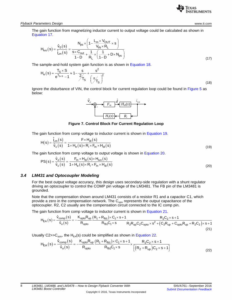
Ignore the disturbance of VIN, the control block for current regulation loop could be found in Figure 5 asbelow:
Figure 7. Control Block For Current Regulation Loop
The gain function from comp voltage to inductor current is shown in Equation 19.
(19)
The gain function from comp voltage to output voltage is shown in Equation 20.
(20)
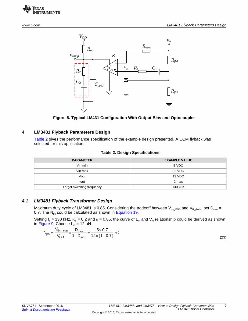
3.4 LM431 and Optocoupler ModelingFor the best output voltage accuracy, this design uses secondary-side regulation with a shunt regulatordriving an optocoupler to control the COMP pin voltage of the LM3481. The FB pin of the LM3481 isgrounded.
Note that the compensation shown around LM431 consists of a resistor R1 and a capacitor C1, whichprovide a zero in the compensation network. The Copto represents the output capacitance of theoptocoupler. R2, C2 usually are the compensation circuit connected to the IC comp pin.
The gain function from comp voltage to inductor current is shown in Equation 21.
(21)
Usually C2>>Copto, the HEA(s) could be simplified as shown in Equation 22.
(22)
� �IN_
psOUT
V D 5 0.7N 1
V 1 D 12 1 0.7u
u |� u �
min max
max
voVDD
R1 C1
Ropto
Rfb1
Rfb2
R2
Rup
C2 Copto
vcomp
vx
K
www.ti.com LM3481 Flyback Parameters Design
9SNVA761–September 2016Submit Documentation Feedback
Copyright © 2016, Texas Instruments Incorporated
LM3481, LM3488, and LM3478 – How to Design Flyback Converter WithLM3481 Boost Controller
Figure 8. Typical LM431 Configuration With Output Bias and Optocoupler
4 LM3481 Flyback Parameters DesignTable 2 gives the performance specification of the example design presented. A CCM flyback wasselected for this application.
Table 2. Design Specifications
PARAMETER EXAMPLE VALUEVin min 5 VDCVin max 32 VDC
Vout 12 VDCIout 2 max
Target switching frequency 130 kHz
4.1 LM3481 Flyback Transformer DesignMaximum duty cycle of LM3481 is 0.85. Considering the tradeoff between Vds_MOS and VR_diode, set Dmax =0.7. The Nps could be calculated as shown in Equation 19.
Setting fs = 130 kHz, KL = 0.2 and η = 0.85, the curve of Lm and Vin relationship could be derived as shownin Figure 9. Choose Lm = 12 µH.
(23)
� �3 3sLin
n i e mm s n e s
V DV 1S R 6 10 ; S 5.85 10 ;F 10.97
L T S S T
u u u u
�
� �
� �� �
2 2L LMOUT OUT
dsRMSIN
2L LM ps2
R _ diode OUT
K IV II D 10.86 A
V D 3
K I NI 1 D I 9.31 A
3
§ ·u§ ·u¨ ¸ u � ¨ ¸¨ ¸u© ¹© ¹
§ ·u u¨ ¸ � u � ¨ ¸¨ ¸© ¹
ds _MOS in _max o ps
ds _ diode o in _max ps
V V V N 44 V
V V V / N 44 V
� u
�
� �o IN_min OUT psLpk _Lm
IN_min OUT ps
P V V NKI 1 9.13 A
2 V V N
u � u§ · � u ¨ ¸ u uKu© ¹
0
4.0
8.0
12.0
Lm(u
H)
5 14 23 32Vin(V)
LM3481 Flyback Parameters Design www.ti.com
10 SNVA761–September 2016Submit Documentation Feedback
Copyright © 2016, Texas Instruments Incorporated
LM3481, LM3488, and LM3478 – How to Design Flyback Converter WithLM3481 Boost Controller
Figure 9. The Curve of Lm and Vin Relationship
Peak Primary Winding current can be calculated as shown below:
(24)
Use 30% to 40% headroom on the Peak primary current to calculate the current sense resistor.
The limit on the ISEN pin of LM3481 is 100 mV so the current sense resistance can be chosen as100 mV / 12 A = 8.33 mΩ. A current sense resistance of 6 mΩ was chosen for this application.
4.2 LM3481 Flyback MOSFET and Diode SelectionAccording to Equation 6, the voltage stress of MOSFET and Diode is:
(25)
(26)
To get good thermal performance, reasonable package for diode and MOSFET are needed to be chosenbeside ensuring required voltage/current rating. Here MOSFET CSD19502Q5B (80V/100A, DNK0008A)and diode V10P-M3/86A (100V/10A, TO-227) are chosen.
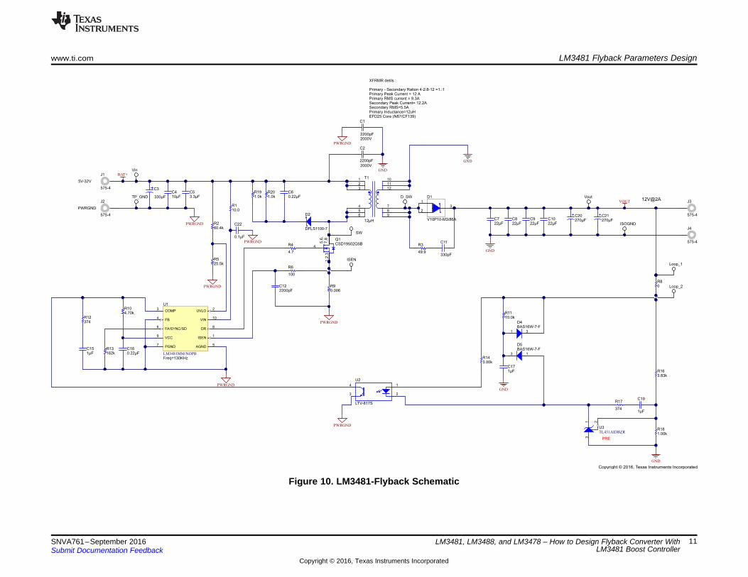
4.3 LM3481 Flyback CCM Flyback Transfer FunctionFigure 10 shows the final application schematic of the flyback solution based on LM3481.
LM3481 has an internal VsL (90 mV) slope compensation to avoid sub-harmonic oscillation when dutycycle is larger than 0.5. In 12Vin and 12-V, 2-A output condition, the modulator gain of the circuit Fm couldbe derived as shown in Equation 27.
(27)
FB4
ISEN1
UVLO2
DR8
FA/SYNC/SD6
VIN10
COMP3
PGND7
AGND5
VCC9
U1
LM3481MM/NOPB
2200pF2000V
C1
2200pF
2000V
C2
GND
GND
PWRGND
PRE
A1
K3
BAS16W-7-FD4
A1
K3
BAS16W-7-FD5
10.0kR11
GND
GND
0.22µFC16
4.7
R4
PWRGND
PWRGND
PWRGND
PWRGND
PWRGND
5V-32V
PWRGND
4.70kR10
162kR13
GND
XFRMR detils :
Primary - Secondary Ration 4-2:8-12 =1.:1Primary Peak Current = 12 APrimary RMS current = 9.3ASecondary Peak Current= 12.2ASecondary RMS=5.5APrimary Inductance=12uHEFD25 Core (N87/CF139)
J1
575-4
J2
575-4
J3
575-4
J4
575-4
12V@2A
1
2
4
3
U2
LTV-817S
VOUT
BAT+
330µF
C3
10µFC4
25.5kR5
60.4kR2
4
7,8
1,2
,3
5,6
,
Q1CSD19502Q5B
100
R6
2200pFC12
1
3
2
D1
V10P10-M3/86A12µH
1
2
3
4
5
6
7
8
9
10
11
12
T1
3.83kR16
1.00kR18
3.00kR14
0.22µFC6
49.9
R3
330pF
C11
Freq=130KHz
SW
Vout
Loop_1
Loop_2
ISOGND
Vin
TP_GND
ISEN
D_SW
270µFC21
0.006R9
374
R17
10.0R1
0.1µF
C22
PWRGND
D2
DFLS1100-7
1.0kR19
1.0kR20
270µFC20
0R8
1µFC15
1µFC17
1µF
C19
374R12
3.3µFC5
22µFC7
22µFC8
22µFC9
22µFC10
3
21
U3TL431AIDBZR
Copyright © 2016, Texas Instruments Incorporated
www.ti.com LM3481 Flyback Parameters Design
11SNVA761–September 2016Submit Documentation Feedback
Copyright © 2016, Texas Instruments Incorporated
LM3481, LM3488, and LM3478 – How to Design Flyback Converter WithLM3481 Boost Controller
Figure 10. LM3481-Flyback Schematic

s 100
0
Phas
e_Po
wer
stag
e(de
g)
1 10 102 103 104 105 106
Frequency(Hz)
s 200
s 300
s 400
s�20
0
20
40
60
Gai
n_Po
wer
stag
e(dB
)
s�40
s�601 10 102 103 104 105 106
Frequency(Hz)
LM3481 Flyback Parameters Design www.ti.com
12 SNVA761–September 2016Submit Documentation Feedback
Copyright © 2016, Texas Instruments Incorporated
LM3481, LM3488, and LM3478 – How to Design Flyback Converter WithLM3481 Boost Controller
According to Equation 11 to Equation 16, Hdi(s), Hivo(s), He(s) and H(s) transfer function could bederived. Figure 11 shows the Mathcad calculated Bode plot of LM3481 flyback converter, and Figure 12shows the simplis simulation schematic and results. It could be observed that the right half plane zero offlyback converter is at 33.2 kHz. The calculated results match the simulation results very well.
Figure 11. Calculated LM3481-Flyback Bode Plot – Gain-Frequency
Figure 12. Calculated LM3481-Flyback Bode Plot –Phase-Frequency
www.ti.com LM3481 Flyback Parameters Design
13SNVA761–September 2016Submit Documentation Feedback
Copyright © 2016, Texas Instruments Incorporated
LM3481, LM3488, and LM3478 – How to Design Flyback Converter WithLM3481 Boost Controller
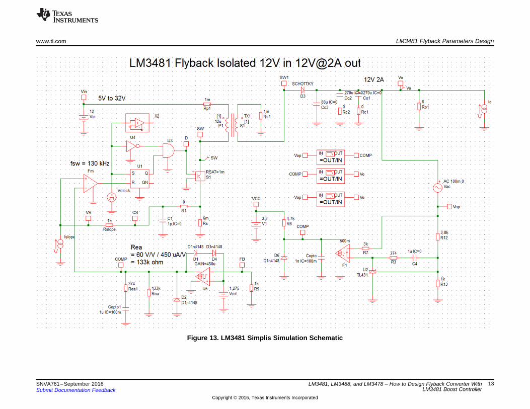
Figure 13. LM3481 Simplis Simulation Schematic
� �16.2 20fb1 opto
1opto up
10 R RR 374 ;
K R
�u u
:u
o reffb1 fb2
ref
V VR R 3.8 k ;
V
� u :
LM3481 Flyback Parameters Design www.ti.com
14 SNVA761–September 2016Submit Documentation Feedback
Copyright © 2016, Texas Instruments Incorporated
LM3481, LM3488, and LM3478 – How to Design Flyback Converter WithLM3481 Boost Controller
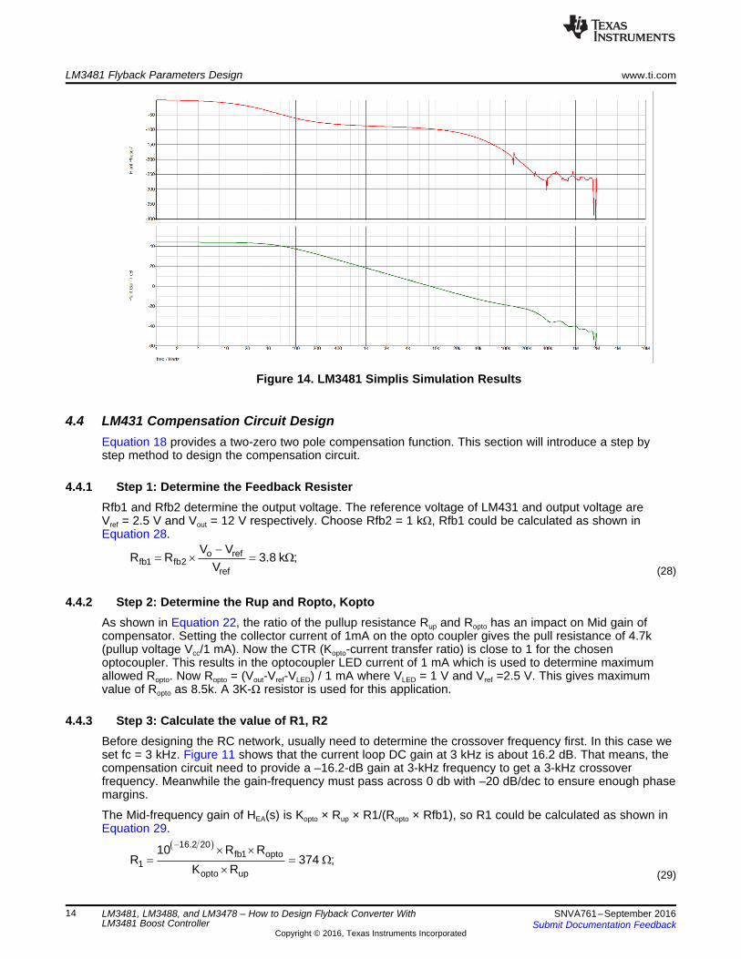
Figure 14. LM3481 Simplis Simulation Results
4.4 LM431 Compensation Circuit DesignEquation 18 provides a two-zero two pole compensation function. This section will introduce a step bystep method to design the compensation circuit.
4.4.1 Step 1: Determine the Feedback ResisterRfb1 and Rfb2 determine the output voltage. The reference voltage of LM431 and output voltage areVref = 2.5 V and Vout = 12 V respectively. Choose Rfb2 = 1 kΩ, Rfb1 could be calculated as shown inEquation 28.
(28)
4.4.2 Step 2: Determine the Rup and Ropto, KoptoAs shown in Equation 22, the ratio of the pullup resistance Rup and Ropto has an impact on Mid gain ofcompensator. Setting the collector current of 1mA on the opto coupler gives the pull resistance of 4.7k(pullup voltage Vcc/1 mA). Now the CTR (Kopto-current transfer ratio) is close to 1 for the chosenoptocoupler. This results in the optocoupler LED current of 1 mA which is used to determine maximumallowed Ropto. Now Ropto = (Vout-Vref-VLED) / 1 mA where VLED = 1 V and Vref =2.5 V. This gives maximumvalue of Ropto as 8.5k. A 3K-Ω resistor is used for this application.
4.4.3 Step 3: Calculate the value of R1, R2Before designing the RC network, usually need to determine the crossover frequency first. In this case weset fc = 3 kHz. Figure 11 shows that the current loop DC gain at 3 kHz is about 16.2 dB. That means, thecompensation circuit need to provide a –16.2-dB gain at 3-kHz frequency to get a 3-kHz crossoverfrequency. Meanwhile the gain-frequency must pass across 0 db with –20 dB/dec to ensure enough phasemargins.
The Mid-frequency gain of HEA(s) is Kopto × Rup × R1/(Ropto × Rfb1), so R1 could be calculated as shown inEquation 29.
(29)

Frequency(Hz)
0
Gai
n_C
ompe
nsat
ion(
dB)
1 10 102 103 104 105 106s 20
20
40 180
Phas
e_C
ompe
nsat
ion(
deg)
1 10 102 103 104 105 106
Frequency(Hz)
140
160
120
100
80
1 21
1C C 1 F
2 R P
Su
www.ti.com LM3481 Flyback Parameters Design
15SNVA761–September 2016Submit Documentation Feedback
Copyright © 2016, Texas Instruments Incorporated
LM3481, LM3488, and LM3478 – How to Design Flyback Converter WithLM3481 Boost Controller
To reduce the variables and simplify the design, setting R2=R1=374 Ω. Then the compensation transferfunction could be considered as one-pole one-zero system.
4.4.4 Step 4: Calculate the Value of C1, C2The RC network (R1C1 and R2C2) is used to provide a zero to boost the phase and are placed below thecrossover frequency. In this application zero were set at fzero = 400 Hz. C1 and C2 could be calculated asshown in Equation 29.
(30)
Figure 15 shows the Mathcad calculated Bode plot of compensation circuit, and Figure 17 shows thesimplis simulation schematic and results. It could be observed that the calculated results and simulationresults matched well.
Figure 15. Compensation Circuit Bode Plot CalculatedResults – Gain-Frequency
Figure 16. Compensation Circuit Bode Plot CalculatedResults – Phase-Frequency
Figure 17. Compensation Simplis Simulation Results
4.5 LM3481 Flyback Loop Response PerformanceFigure 18 and Figure 20 show the calculated and simulation results of LM3481 flyback aftercompensation. It could be observed that the crossover frequency Fc is exactly at 3 kHz and there is about77° of phase margin. The calculated results and simulation results matched well.

102 103 104 105
Frequency(Hz)
Gai
n_T
Loo
p(dB
)
s 50
s 25
0
50
25
102 103 104 105
Frequency(Hz)
s 200
s 100
0
100
200
Phas
e_T
Loo
p(de
g)
Bench Verification www.ti.com
16 SNVA761–September 2016Submit Documentation Feedback
Copyright © 2016, Texas Instruments Incorporated
LM3481, LM3488, and LM3478 – How to Design Flyback Converter WithLM3481 Boost Controller
Figure 18. LM3481 Flyback Bode Plot CalculatedResults – Gain-Frequency
Figure 19. LM3481 Flyback Bode Plot CalculatedResults – Phase-Frequency
Figure 20. LM3481 Flyback Bode Plot Simulation Results
5 Bench VerificationFigure 21 and Figure 22 show the output voltage ripple and rectifier diode switching waveform (anode toISO GND) for the LM3481-FlybackEVM. The output current is the rated full load of 2 A and at of VIN = 5.5V and 28 V respectively. It can be observed that the design works in CCM mode over wide input range.
www.ti.com Conclusion
17SNVA761–September 2016Submit Documentation Feedback
Copyright © 2016, Texas Instruments Incorporated
LM3481, LM3488, and LM3478 – How to Design Flyback Converter WithLM3481 Boost Controller
Figure 21. Maximum Output Ripple at Different InputVoltage – VIN = 5.5 V
Figure 22. Maximum Output Ripple at Different InputVoltage – VIN = 28 V
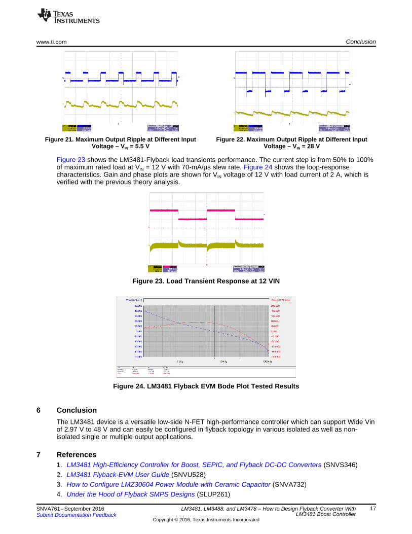
Figure 23 shows the LM3481-Flyback load transients performance. The current step is from 50% to 100%of maximum rated load at VIN = 12 V with 70-mA/µs slew rate. Figure 24 shows the loop-responsecharacteristics. Gain and phase plots are shown for VIN voltage of 12 V with load current of 2 A, which isverified with the previous theory analysis.
Figure 23. Load Transient Response at 12 VIN
Figure 24. LM3481 Flyback EVM Bode Plot Tested Results
6 ConclusionThe LM3481 device is a versatile low-side N-FET high-performance controller which can support Wide Vinof 2.97 V to 48 V and can easily be configured in flyback topology in various isolated as well as non-isolated single or multiple output applications.
7 References1. LM3481 High-Efficiency Controller for Boost, SEPIC, and Flyback DC-DC Converters (SNVS346)2. LM3481 Flyback-EVM User Guide (SNVU528)3. How to Configure LMZ30604 Power Module with Ceramic Capacitor (SNVA732)4. Under the Hood of Flyback SMPS Designs (SLUP261)

IMPORTANT NOTICE
Texas Instruments Incorporated and its subsidiaries (TI) reserve the right to make corrections, enhancements, improvements and otherchanges to its semiconductor products and services per JESD46, latest issue, and to discontinue any product or service per JESD48, latestissue. Buyers should obtain the latest relevant information before placing orders and should verify that such information is current andcomplete. All semiconductor products (also referred to herein as “components”) are sold subject to TI’s terms and conditions of salesupplied at the time of order acknowledgment.TI warrants performance of its components to the specifications applicable at the time of sale, in accordance with the warranty in TI’s termsand conditions of sale of semiconductor products. Testing and other quality control techniques are used to the extent TI deems necessaryto support this warranty. Except where mandated by applicable law, testing of all parameters of each component is not necessarilyperformed.TI assumes no liability for applications assistance or the design of Buyers’ products. Buyers are responsible for their products andapplications using TI components. To minimize the risks associated with Buyers’ products and applications, Buyers should provideadequate design and operating safeguards.TI does not warrant or represent that any license, either express or implied, is granted under any patent right, copyright, mask work right, orother intellectual property right relating to any combination, machine, or process in which TI components or services are used. Informationpublished by TI regarding third-party products or services does not constitute a license to use such products or services or a warranty orendorsement thereof. Use of such information may require a license from a third party under the patents or other intellectual property of thethird party, or a license from TI under the patents or other intellectual property of TI.Reproduction of significant portions of TI information in TI data books or data sheets is permissible only if reproduction is without alterationand is accompanied by all associated warranties, conditions, limitations, and notices. TI is not responsible or liable for such altereddocumentation. Information of third parties may be subject to additional restrictions.Resale of TI components or services with statements different from or beyond the parameters stated by TI for that component or servicevoids all express and any implied warranties for the associated TI component or service and is an unfair and deceptive business practice.TI is not responsible or liable for any such statements.Buyer acknowledges and agrees that it is solely responsible for compliance with all legal, regulatory and safety-related requirementsconcerning its products, and any use of TI components in its applications, notwithstanding any applications-related information or supportthat may be provided by TI. Buyer represents and agrees that it has all the necessary expertise to create and implement safeguards whichanticipate dangerous consequences of failures, monitor failures and their consequences, lessen the likelihood of failures that might causeharm and take appropriate remedial actions. Buyer will fully indemnify TI and its representatives against any damages arising out of the useof any TI components in safety-critical applications.In some cases, TI components may be promoted specifically to facilitate safety-related applications. With such components, TI’s goal is tohelp enable customers to design and create their own end-product solutions that meet applicable functional safety standards andrequirements. Nonetheless, such components are subject to these terms.No TI components are authorized for use in FDA Class III (or similar life-critical medical equipment) unless authorized officers of the partieshave executed a special agreement specifically governing such use.Only those TI components which TI has specifically designated as military grade or “enhanced plastic” are designed and intended for use inmilitary/aerospace applications or environments. Buyer acknowledges and agrees that any military or aerospace use of TI componentswhich have not been so designated is solely at the Buyer's risk, and that Buyer is solely responsible for compliance with all legal andregulatory requirements in connection with such use.TI has specifically designated certain components as meeting ISO/TS16949 requirements, mainly for automotive use. In any case of use ofnon-designated products, TI will not be responsible for any failure to meet ISO/TS16949.
Products ApplicationsAudio www.ti.com/audio Automotive and Transportation www.ti.com/automotiveAmplifiers amplifier.ti.com Communications and Telecom www.ti.com/communicationsData Converters dataconverter.ti.com Computers and Peripherals www.ti.com/computersDLP® Products www.dlp.com Consumer Electronics www.ti.com/consumer-appsDSP dsp.ti.com Energy and Lighting www.ti.com/energyClocks and Timers www.ti.com/clocks Industrial www.ti.com/industrialInterface interface.ti.com Medical www.ti.com/medicalLogic logic.ti.com Security www.ti.com/securityPower Mgmt power.ti.com Space, Avionics and Defense www.ti.com/space-avionics-defenseMicrocontrollers microcontroller.ti.com Video and Imaging www.ti.com/videoRFID www.ti-rfid.comOMAP Applications Processors www.ti.com/omap TI E2E Community e2e.ti.comWireless Connectivity www.ti.com/wirelessconnectivity
Mailing Address: Texas Instruments, Post Office Box 655303, Dallas, Texas 75265Copyright © 2016, Texas Instruments Incorporated


![Catalogue FLYBACK Equivalent - [PDF Document] FLYBACK Equivalent FlyBack Equivalent flyback reemplazo conversor Flyback tv fly-back Flyback Tester Flyback Converter conversor Flyback](https://img.pdfslide.us/doc/110x75/5a832a447f8b9a9d308e9416/catalogue-flyback-equivalent-pdf-document-flyback-equivalent-flyback-equivalent.jpg)