Embed Size (px)
Citation preview
VOUT = 2.5V/2A
CINCOUT
RFB1
RFB2
L1
D1
Q1
10 PF100 PF
10 PH
1k
2.15k
Si2343
LM3475
VIN
EN
GND
PGATE
FB1
2
3
4
5
CFF
1 nF
VIN = 5V
Product
Folder
Sample &Buy
Technical
Documents
Tools &
Software
Support &Community
LM3475SNVS239C –OCTOBER 2004–REVISED OCTOBER 2015
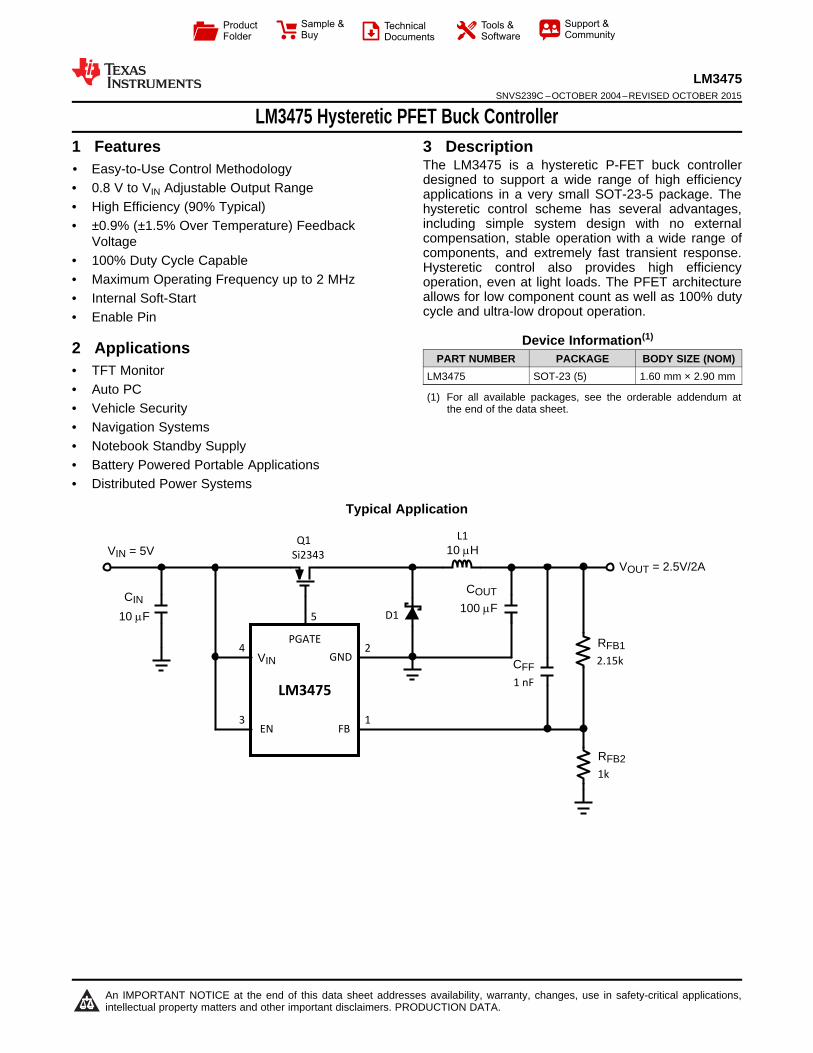
LM3475 Hysteretic PFET Buck Controller1 Features 3 Description
The LM3475 is a hysteretic P-FET buck controller1• Easy-to-Use Control Methodology
designed to support a wide range of high efficiency• 0.8 V to VIN Adjustable Output Range applications in a very small SOT-23-5 package. The• High Efficiency (90% Typical) hysteretic control scheme has several advantages,
including simple system design with no external• ±0.9% (±1.5% Over Temperature) Feedbackcompensation, stable operation with a wide range ofVoltagecomponents, and extremely fast transient response.• 100% Duty Cycle Capable Hysteretic control also provides high efficiency
• Maximum Operating Frequency up to 2 MHz operation, even at light loads. The PFET architectureallows for low component count as well as 100% duty• Internal Soft-Startcycle and ultra-low dropout operation.• Enable Pin
Device Information(1)2 Applications
PART NUMBER PACKAGE BODY SIZE (NOM)• TFT Monitor LM3475 SOT-23 (5) 1.60 mm × 2.90 mm• Auto PC (1) For all available packages, see the orderable addendum at• Vehicle Security the end of the data sheet.
• Navigation Systems• Notebook Standby Supply• Battery Powered Portable Applications• Distributed Power Systems
Typical Application
1
An IMPORTANT NOTICE at the end of this data sheet addresses availability, warranty, changes, use in safety-critical applications,intellectual property matters and other important disclaimers. PRODUCTION DATA.
LM3475SNVS239C –OCTOBER 2004–REVISED OCTOBER 2015 www.ti.com
Table of Contents7.4 Device Functional Modes........................................ 101 Features .................................................................. 1
8 Application and Implementation ........................ 112 Applications ........................................................... 18.1 Application Information............................................ 113 Description ............................................................. 18.2 Typical Application ................................................. 114 Revision History..................................................... 2
9 Power Supply Recommendations ...................... 165 Pin Configuration and Functions ......................... 310 Layout................................................................... 166 Specifications......................................................... 4
10.1 Layout Guidelines ................................................. 166.1 Absolute Maximum Ratings ...................................... 410.2 Layout Example .................................................... 176.2 ESD Ratings.............................................................. 4
11 Device and Documentation Support ................. 186.3 Recommended Operating Ratings ........................... 411.1 Device Support...................................................... 186.4 Thermal Information .................................................. 411.2 Community Resources.......................................... 186.5 Electrical Characteristics........................................... 511.3 Trademarks ........................................................... 186.6 Typical Characteristics .............................................. 611.4 Electrostatic Discharge Caution............................ 187 Detailed Description .............................................. 811.5 Glossary ................................................................ 187.1 Overview ................................................................... 8
12 Mechanical, Packaging, and Orderable7.2 Functional Block Diagram ......................................... 8Information ........................................................... 187.3 Feature Description................................................... 8
4 Revision HistoryNOTE: Page numbers for previous revisions may differ from page numbers in the current version.
Changes from Revision B (March 2013) to Revision C Page
• Added ESD Ratings table, Feature Description section, Device Functional Modes, Application and Implementationsection, Power Supply Recommendations section, Layout section, Device and Documentation Support section, andMechanical, Packaging, and Orderable Information section. ................................................................................................. 1
Changes from Revision A (March 2013) to Revision B Page
• Changed layout of National Data Sheet to TI format. ........................................................................................................... 1
2 Submit Documentation Feedback Copyright © 2004–2015, Texas Instruments Incorporated
Product Folder Links: LM3475
PGATE
GND
FB
VIN
1
2
3 4
5
EN
LM3475www.ti.com SNVS239C –OCTOBER 2004–REVISED OCTOBER 2015
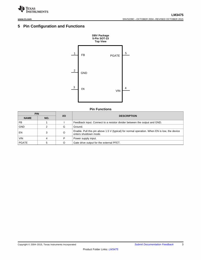
5 Pin Configuration and Functions
DBV Package5-Pin SOT-23
Top View
Pin FunctionsPIN
I/O DESCRIPTIONNAME NO.
FB 1 I Feedback input. Connect to a resistor divider between the output and GND.GND 2 G Ground.
Enable. Pull this pin above 1.5 V (typical) for normal operation. When EN is low, the deviceEN 3 O enters shutdown mode.VIN 4 P Power supply input.PGATE 5 O Gate drive output for the external PFET.
Copyright © 2004–2015, Texas Instruments Incorporated Submit Documentation Feedback 3
Product Folder Links: LM3475
LM3475SNVS239C –OCTOBER 2004–REVISED OCTOBER 2015 www.ti.com
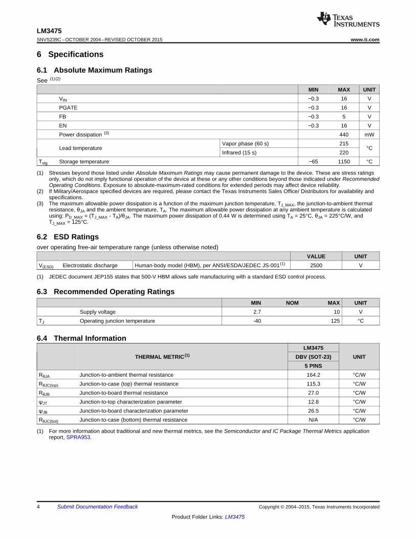
6 Specifications
6.1 Absolute Maximum RatingsSee (1) (2)
MIN MAX UNITVIN −0.3 16 VPGATE −0.3 16 VFB −0.3 5 VEN −0.3 16 VPower dissipation (3) 440 mW
Vapor phase (60 s) 215Lead temperature °C
Infrared (15 s) 220Tstg Storage temperature −65 1150 °C
(1) Stresses beyond those listed under Absolute Maximum Ratings may cause permanent damage to the device. These are stress ratingsonly, which do not imply functional operation of the device at these or any other conditions beyond those indicated under RecommendedOperating Conditions. Exposure to absolute-maximum-rated conditions for extended periods may affect device reliability.
(2) If Military/Aerospace specified devices are required, please contact the Texas Instruments Sales Office/ Distributors for availability andspecifications.
(3) The maximum allowable power dissipation is a function of the maximum junction temperature, TJ_MAX, the junction-to-ambient thermalresistance, θJA and the ambient temperature, TA. The maximum allowable power dissipation at any ambient temperature is calculatedusing: PD_MAX = (TJ_MAX - TA)/θJA. The maximum power dissipation of 0.44 W is determined using TA = 25°C, θJA = 225°C/W, andTJ_MAX = 125°C.
6.2 ESD Ratingsover operating free-air temperature range (unless otherwise noted)
VALUE UNITV(ESD) Electrostatic discharge Human-body model (HBM), per ANSI/ESDA/JEDEC JS-001 (1) 2500 V
(1) JEDEC document JEP155 states that 500-V HBM allows safe manufacturing with a standard ESD control process.
6.3 Recommended Operating RatingsMIN NOM MAX UNIT
Supply voltage 2.7 10 VTJ Operating junction temperature -40 125 °C
6.4 Thermal InformationLM3475
THERMAL METRIC (1) DBV (SOT-23) UNIT5 PINS
RθJA Junction-to-ambient thermal resistance 164.2 °C/WRθJC(top) Junction-to-case (top) thermal resistance 115.3 °C/WRθJB Junction-to-board thermal resistance 27.0 °C/WψJT Junction-to-top characterization parameter 12.8 °C/WψJB Junction-to-board characterization parameter 26.5 °C/WRθJC(bot) Junction-to-case (bottom) thermal resistance N/A °C/W
(1) For more information about traditional and new thermal metrics, see the Semiconductor and IC Package Thermal Metrics applicationreport, SPRA953.
4 Submit Documentation Feedback Copyright © 2004–2015, Texas Instruments Incorporated
Product Folder Links: LM3475
LM3475www.ti.com SNVS239C –OCTOBER 2004–REVISED OCTOBER 2015
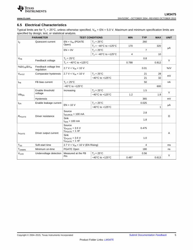
6.5 Electrical CharacteristicsTypical limits are for TJ = 25°C, unless otherwise specified, VIN = EN = 5.0 V. Maximum and minimum specification limits arespecified by design, test, or statistical analysis.
PARAMETER TEST CONDITIONS MIN TYP MAX UNITIQ Quiescent current EN = VIN (PGATE TJ = 25°C 260
Open) TJ = −40°C to +125°C 170 320µA
EN = 0V TJ = 25°C 7TJ = −40°C to +125°C 4 10
VFB TJ = 25°C 0.8Feedback voltage V
TJ = −40°C to +125°C 0.788 0.812%ΔVFB/ΔVIN Feedback voltage line 2.7 V < VIN < 10 V 0.01 %/VregulationVHYST Comparator hysteresis 2.7 V < VIN < 10 V TJ = 25°C 21 28
mV−40°C to +125°C 21 32
IFB FB bias current TJ = 25°C 50 nA−40°C to +125°C 600
Enable threshold Increasing TJ = 25°C 1.5VvoltageVthEN −40°C to +125°C 1.2 1.8
Hysteresis 365 mVIEN Enable leakage current TJ = 25°C 0.025
EN = 10 V µA−40°C to +125°C 1
Source 2.8ISOURCE = 100 mARPGATE Driver resistance Ω
Sink 1.8ISink = 100 mASourceVPGATE = 3.5 V 0.475CPGATE = 1 nF
IPGATE Driver output current ASinkVPGATE = 3.5 V 1.0CPGATE = 1 nF
TSS Soft-start time 2.7 V < VIN < 10 V (EN Rising) 4 msTONMIN Minimum on-time PGATE Open 180 nsVUVD Undervoltage detection Measured at the FB TJ = 25°C 0.56
VPin −40°C to +125°C 0.487 0.613
Copyright © 2004–2015, Texas Instruments Incorporated Submit Documentation Feedback 5
Product Folder Links: LM3475
4 5 6 7 8 9 10
INPUT VOLTAGE (VIN)
0
20
40
60
80
100
EF
FIC
IEN
CY
(%
)
84
86
88
90
92
94
96
98
EF
FIC
IEN
CY
(%
)
OUTPUT CURRENT (A)
0.5 1 1.5 2
LM3475SNVS239C –OCTOBER 2004–REVISED OCTOBER 2015 www.ti.com
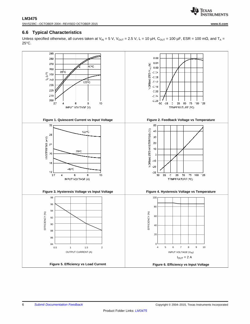
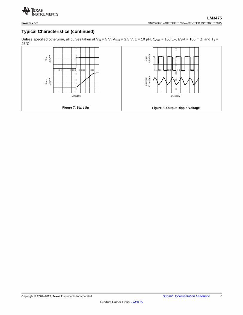
6.6 Typical CharacteristicsUnless specified otherwise, all curves taken at VIN = 5 V, VOUT = 2.5 V, L = 10 µH, COUT = 100 µF, ESR = 100 mΩ, and TA =25°C.
Figure 1. Quiescent Current vs Input Voltage Figure 2. Feedback Voltage vs Temperature
Figure 3. Hysteresis Voltage vs Input Voltage Figure 4. Hysteresis Voltage vs Temperature
IOUT = 2 A
Figure 5. Efficiency vs Load Current Figure 6. Efficiency vs Input Voltage
6 Submit Documentation Feedback Copyright © 2004–2015, Texas Instruments Incorporated
Product Folder Links: LM3475
VS
W
2.5V
/DIV
VR
IPP
LE
20 m
V/D
IV
2 Ps/DIV
VIN
2V/D
IV
VO
UT
1V/D
IV
1 ms/DIV
LM3475www.ti.com SNVS239C –OCTOBER 2004–REVISED OCTOBER 2015
Typical Characteristics (continued)Unless specified otherwise, all curves taken at VIN = 5 V, VOUT = 2.5 V, L = 10 µH, COUT = 100 µF, ESR = 100 mΩ, and TA =25°C.
Figure 7. Start Up Figure 8. Output Ripple Voltage
Copyright © 2004–2015, Texas Instruments Incorporated Submit Documentation Feedback 7
Product Folder Links: LM3475
PGATE
GND
Internal
Regulator
VCC
Level
Shiften
Band Gap
Reference VREF
70% VREF
Soft-Start
Vref Ramp
+
-
+
-
Current
Biasreset
Blanking
Timer
UVD-Disable
UVD-Disable
en
reset
FB
EN
VINPdrive
UVD
Comp
Hysteretic
Comp
LM3475SNVS239C –OCTOBER 2004–REVISED OCTOBER 2015 www.ti.com
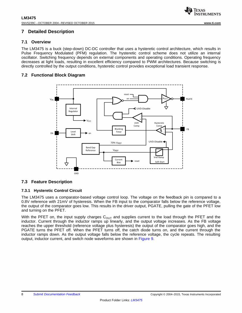
7 Detailed Description
7.1 OverviewThe LM3475 is a buck (step-down) DC-DC controller that uses a hysteretic control architecture, which results inPulse Frequency Modulated (PFM) regulation. The hysteretic control scheme does not utilize an internaloscillator. Switching frequency depends on external components and operating conditions. Operating frequencydecreases at light loads, resulting in excellent efficiency compared to PWM architectures. Because switching isdirectly controlled by the output conditions, hysteretic control provides exceptional load transient response.
7.2 Functional Block Diagram
7.3 Feature Description
7.3.1 Hysteretic Control CircuitThe LM3475 uses a comparator-based voltage control loop. The voltage on the feedback pin is compared to a0.8V reference with 21mV of hysteresis. When the FB input to the comparator falls below the reference voltage,the output of the comparator goes low. This results in the driver output, PGATE, pulling the gate of the PFET lowand turning on the PFET.
With the PFET on, the input supply charges COUT and supplies current to the load through the PFET and theinductor. Current through the inductor ramps up linearly, and the output voltage increases. As the FB voltagereaches the upper threshold (reference voltage plus hysteresis) the output of the comparator goes high, and thePGATE turns the PFET off. When the PFET turns off, the catch diode turns on, and the current through theinductor ramps down. As the output voltage falls below the reference voltage, the cycle repeats. The resultingoutput, inductor current, and switch node waveforms are shown in Figure 9.
8 Submit Documentation Feedback Copyright © 2004–2015, Texas Instruments Incorporated
Product Folder Links: LM3475
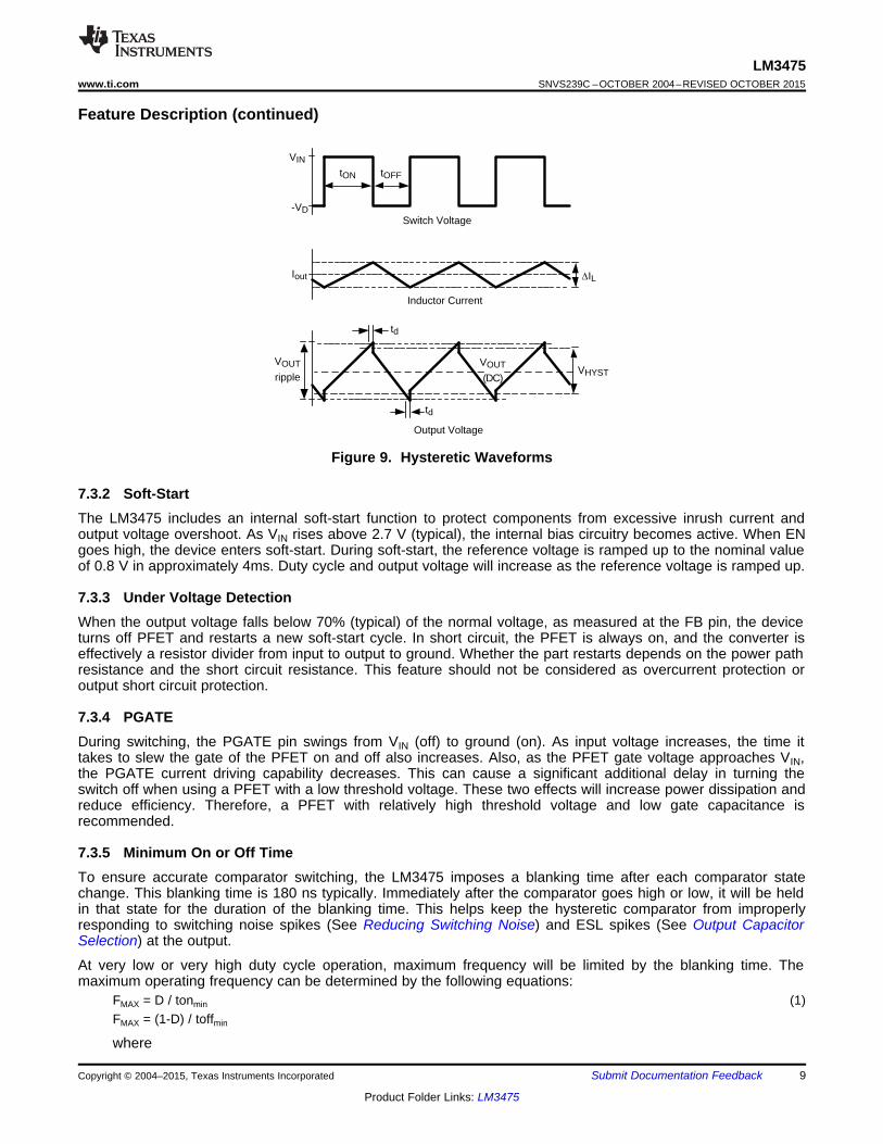
td
VOUT
(DC)VHYST
VOUT
ripple
VIN
-VD
tON
Switch Voltage
Iout 'IL
Inductor Current
Output Voltage
tOFF
td
LM3475www.ti.com SNVS239C –OCTOBER 2004–REVISED OCTOBER 2015
Feature Description (continued)
Figure 9. Hysteretic Waveforms
7.3.2 Soft-StartThe LM3475 includes an internal soft-start function to protect components from excessive inrush current andoutput voltage overshoot. As VIN rises above 2.7 V (typical), the internal bias circuitry becomes active. When ENgoes high, the device enters soft-start. During soft-start, the reference voltage is ramped up to the nominal valueof 0.8 V in approximately 4ms. Duty cycle and output voltage will increase as the reference voltage is ramped up.
7.3.3 Under Voltage DetectionWhen the output voltage falls below 70% (typical) of the normal voltage, as measured at the FB pin, the deviceturns off PFET and restarts a new soft-start cycle. In short circuit, the PFET is always on, and the converter iseffectively a resistor divider from input to output to ground. Whether the part restarts depends on the power pathresistance and the short circuit resistance. This feature should not be considered as overcurrent protection oroutput short circuit protection.
7.3.4 PGATEDuring switching, the PGATE pin swings from VIN (off) to ground (on). As input voltage increases, the time ittakes to slew the gate of the PFET on and off also increases. Also, as the PFET gate voltage approaches VIN,the PGATE current driving capability decreases. This can cause a significant additional delay in turning theswitch off when using a PFET with a low threshold voltage. These two effects will increase power dissipation andreduce efficiency. Therefore, a PFET with relatively high threshold voltage and low gate capacitance isrecommended.
7.3.5 Minimum On or Off TimeTo ensure accurate comparator switching, the LM3475 imposes a blanking time after each comparator statechange. This blanking time is 180 ns typically. Immediately after the comparator goes high or low, it will be heldin that state for the duration of the blanking time. This helps keep the hysteretic comparator from improperlyresponding to switching noise spikes (See Reducing Switching Noise) and ESL spikes (See Output CapacitorSelection) at the output.
At very low or very high duty cycle operation, maximum frequency will be limited by the blanking time. Themaximum operating frequency can be determined by the following equations:
FMAX = D / tonmin (1)FMAX = (1-D) / toffmin
where
Copyright © 2004–2015, Texas Instruments Incorporated Submit Documentation Feedback 9
Product Folder Links: LM3475
LM3475SNVS239C –OCTOBER 2004–REVISED OCTOBER 2015 www.ti.com
Feature Description (continued)• D is the duty cycle, defined as VOUT/VIN, and tonmin
• toffmin is the sum of the blanking time, the propagation delay time, and the PFET delay time (see Figure 9) (2)
7.3.6 Enable Pin (EN)The LM3475 provides a shutdown function via the EN pin to disable the device. The device is active when theEN pin is pulled above 1.5 V (typ) and in shutdown mode when EN is below 1.135 V (typ). In shutdown mode,total quiescent current is less than 10 µA. The EN pin can be directly connected to VIN for always-on operation.
7.4 Device Functional ModesThe LM3475 operates in discontinuous conduction mode at light load current and continuous conduction mode atheavy load current. In discontinuous conduction mode, current through the inductor starts at zero and ramps upto the peak, then ramps down to zero. The next cycle starts when the FB voltage reaches the reference voltage.Until then, the inductor current remains zero. Operating frequency is low, as are switching losses. In continuousconduction mode, current always flows through the inductor and never ramps down to zero.
10 Submit Documentation Feedback Copyright © 2004–2015, Texas Instruments Incorporated
Product Folder Links: LM3475
VOUT = 2.5V/2A
CINCOUT
RFB1
RFB2
L1
D1
Q1
10 PF100 PF
10 PH
1k
2.15k
Si2343
LM3475
VIN
EN
GND
PGATE
FB1
2
3
4
5
CFF
1 nF
VIN = 5V
LM3475www.ti.com SNVS239C –OCTOBER 2004–REVISED OCTOBER 2015
8 Application and Implementation
NOTEInformation in the following applications sections is not part of the TI componentspecification, and TI does not warrant its accuracy or completeness. TI’s customers areresponsible for determining suitability of components for their purposes. Customers shouldvalidate and test their design implementation to confirm system functionality.
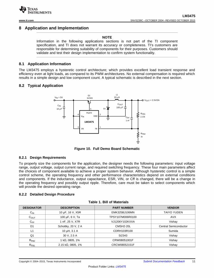
8.1 Application InformationThe LM3475 employs a hysteretic control architecture; which provides excellent load transient response andefficiency even at light loads, as compared to its PWM architectures. No external compensation is required whichresults in a simple design and low component count. A typical schematic is described in the next section.
8.2 Typical Application
Figure 10. Full Demo Board Schematic
8.2.1 Design RequirementsTo properly size the components for the application, the designer needs the following parameters: input voltagerange, output voltage, output current range, and required switching frequency. These four main parameters affectthe choices of component available to achieve a proper system behavior. Although hysteretic control is a simplecontrol scheme, the operating frequency and other performance characteristics depend on external conditionsand components. If the inductance, output capacitance, ESR, VIN, or Cff is changed, there will be a change inthe operating frequency and possibly output ripple. Therefore, care must be taken to select components whichwill provide the desired operating range.
8.2.2 Detailed Design Procedure
Table 1. Bill of MaterialsDESIGNATOR DESCRIPTION PART NUMBER VENDOR
CIN 10 µF, 16 V, X5R EMK325BJ106MN TAIYO YUDENCOUT 100 µF, 6 V, Ta TPSY107M006R0100 AVXCFF 1 nF, 25 V, X7R VJ1206Y102KXXA VishayD1 Schottky, 20 V, 2 A CMSH2-20L Central SemiconductorL1 10 µH, 3.1 A CDRH103R100 SumidaQ1 30 V, 2.5 A Si2343 Vishay
RFB2 1 kΩ, 0805, 1% CRW08051001F VishayRFB1 2.15 kΩ, 0805, 1% CRCW08052151F Vishay
Copyright © 2004–2015, Texas Instruments Incorporated Submit Documentation Feedback 11
Product Folder Links: LM3475
F =(VIN - VOUT) x ESR
x(VHYST x D x L) + (VIN x delay x ESR)VIN
VOUT
-
+
PMOS_drv
Hyst Comp
FB
+
VOUT
PGATE
+-Reference
Voltage
VFB = 0.8V
VHYST = 21 mV
PGATE
R1
R2
L
Cff
COUT
VOUT =R1 + R2
R2x VFB
LM3475SNVS239C –OCTOBER 2004–REVISED OCTOBER 2015 www.ti.com
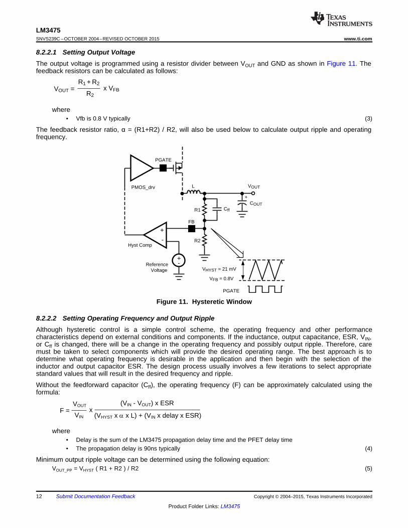
8.2.2.1 Setting Output VoltageThe output voltage is programmed using a resistor divider between VOUT and GND as shown in Figure 11. Thefeedback resistors can be calculated as follows:
where• Vfb is 0.8 V typically (3)
The feedback resistor ratio, α = (R1+R2) / R2, will also be used below to calculate output ripple and operatingfrequency.
Figure 11. Hysteretic Window
8.2.2.2 Setting Operating Frequency and Output RippleAlthough hysteretic control is a simple control scheme, the operating frequency and other performancecharacteristics depend on external conditions and components. If the inductance, output capacitance, ESR, VIN,or Cff is changed, there will be a change in the operating frequency and possibly output ripple. Therefore, caremust be taken to select components which will provide the desired operating range. The best approach is todetermine what operating frequency is desirable in the application and then begin with the selection of theinductor and output capacitor ESR. The design process usually involves a few iterations to select appropriatestandard values that will result in the desired frequency and ripple.
Without the feedforward capacitor (Cff), the operating frequency (F) can be approximately calculated using theformula:
where• Delay is the sum of the LM3475 propagation delay time and the PFET delay time• The propagation delay is 90ns typically (4)
Minimum output ripple voltage can be determined using the following equation:VOUT_PP = VHYST ( R1 + R2 ) / R2 (5)
12 Submit Documentation Feedback Copyright © 2004–2015, Texas Instruments Incorporated
Product Folder Links: LM3475
F =VIN
2S x R1 x C2 x VHYS
'I2
3IOUT
2 +IRMS =
L =VIN - VSD - VOUT
'Ix
FD
LM3475www.ti.com SNVS239C –OCTOBER 2004–REVISED OCTOBER 2015
8.2.2.3 Using a Feed-forward CapacitorThe operating frequency and output ripple voltage can also be significantly influenced using a speed upcapacitor, Cff, as shown in Figure 11. Cff is connected in parallel with the high side feedback resistor, R1. Theoutput ripple causes a current to be sourced or sunk through this capacitor. This current is essentially a squarewave. Since the input to the feedback pin (FB) is a high impedance node, the bulk of the current flows throughR2. This superimposes a square wave ripple voltage on the FB node. The end result is a reduction in outputripple and an increase in operating frequency. When adding Cff, calculate the formula above with α= 1. The valueof Cff depends on the desired operating frequency and the value of R2. A good starting point is 1nF ceramic at100kHz decreasing linearly with increased operating frequency. Also note that as the output voltage isprogrammed below 1.6V, the effect of Cff will decrease significantly.
8.2.2.4 Inductor SelectionThe most important parameters for the inductor are the inductance and the current rating. The LM3475 operatesover a wide frequency range and can use a wide range of inductance values. Minimum inductance can becalculated using the following equation:
where• D is the duty cycle, defined as VOUT/VIN
• ΔI is the allowable inductor ripple current (6)
Maximum allowable inductor ripple current should be calculated as a function of output current (IOUT) as shownbelow:
ΔImax = IOUT x 0.3
The inductor must also be rated to handle the peak current (IPK) and RMS current given by:IPK = (IOUT + ΔI/2) x 1.1 (7)
(8)
The inductance value and the resulting ripple is one of the key parameters controlling operating frequency.
8.2.2.5 Output Capacitor SelectionOnce the desired operating frequency and inductance value are selected, ESR must be selected based onEquation 4. This process may involve a few iterations to select standard ESR and inductance values.
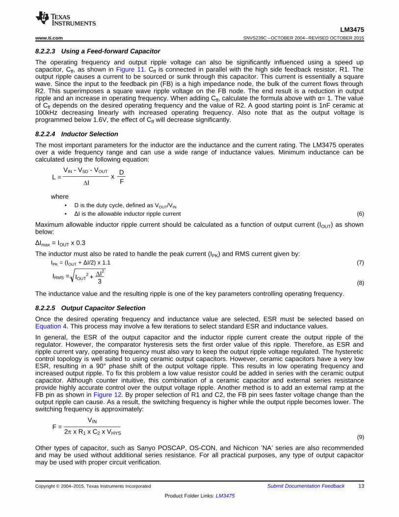
In general, the ESR of the output capacitor and the inductor ripple current create the output ripple of theregulator. However, the comparator hysteresis sets the first order value of this ripple. Therefore, as ESR andripple current vary, operating frequency must also vary to keep the output ripple voltage regulated. The hystereticcontrol topology is well suited to using ceramic output capacitors. However, ceramic capacitors have a very lowESR, resulting in a 90° phase shift of the output voltage ripple. This results in low operating frequency andincreased output ripple. To fix this problem a low value resistor could be added in series with the ceramic outputcapacitor. Although counter intuitive, this combination of a ceramic capacitor and external series resistanceprovide highly accurate control over the output voltage ripple. Another method is to add an external ramp at theFB pin as shown in Figure 12. By proper selection of R1 and C2, the FB pin sees faster voltage change than theoutput ripple can cause. As a result, the switching frequency is higher while the output ripple becomes lower. Theswitching frequency is approximately:
(9)
Other types of capacitor, such as Sanyo POSCAP, OS-CON, and Nichicon ’NA’ series are also recommendedand may be used without additional series resistance. For all practical purposes, any type of output capacitormay be used with proper circuit verification.
Copyright © 2004–2015, Texas Instruments Incorporated Submit Documentation Feedback 13
Product Folder Links: LM3475
VIN VOUT = 0.9V/2A
CINCOUT
RFB1
RFB2
L1
D1
Q1
10 PF 100 PF
10 PH
10k
1.27k
Si2343
LM3475
VIN
EN
GND
PGATE
FB1
2
3
4
5
C2
390 pF
C1
3.9 nF
R1
200k
IRMS_CIN = VIN
IOUTVOUT x (VIN - VOUT)
LM3475SNVS239C –OCTOBER 2004–REVISED OCTOBER 2015 www.ti.com
Capacitors with high ESL (equivalent series inductance) values should not be used. As shown in Figure 9, theoutput ripple voltage contains a small step at both the high and low peaks. This step is caused by and is directlyproportional to the output capacitor’s ESL. A large ESL, such as in an electrolytic capacitor, can create a steplarge enough to cause abnormal switching behavior.
8.2.2.6 Input Capacitor SelectionA bypass capacitor is required between VIN and ground. It must be placed near the source of the external PFET.The input capacitor prevents large voltage transients at the input and provides the instantaneous current whenthe PFET turns on. The important parameters for the input capacitor are the voltage rating and the RMS currentrating. Follow the manufacturer’s recommended voltage de-rating. RMS current and power dissipation (PD) canbe calculated with the equations below:
(10)
Figure 12. External Ramp
8.2.2.7 Diode SelectionThe catch diode provides the current path to the load during the PFET off time. Therefore, the current rating ofthe diode must be higher than the average current through the diode, which be calculated as shown:
ID_AVE = IOUT x (1 − D) (11)
The peak voltage across the catch diode is approximately equal to the input voltage. Therefore, the diode’s peakreverse voltage rating should be greater than 1.3 times the input voltage.
A Schottky diode is recommended, since a low forward voltage drop will improve efficiency.
For high temperature applications, diode leakage current may become significant and require a higher reversevoltage rating to achieve acceptable performance.
8.2.2.8 P-Channel MOSFET SelectionThe PFET switch should be selected based on the maximum Drain-Source voltage (VDS), Drain current rating(ID), maximum Gate-Source voltage (VGS), on resistance (RDSON), and Gate capacitance. The voltage across thePFET when it is turned off is equal to the sum of the input voltage and the diode forward voltage. The VDS mustbe selected to provide some margin beyond the sum of the input voltage and Vd.
Since the current flowing through the PFET is equal to the current through the inductor, ID must be rated higherthan the maximum IPK. During switching, PGATE swings the PFET’s gate from VIN to ground. Therefore, A PFETmust be selected with a maximum VGS larger than VIN. To insure that the PFET turns on completely and quickly,refer to the PGATE section.
14 Submit Documentation Feedback Copyright © 2004–2015, Texas Instruments Incorporated
Product Folder Links: LM3475
5PGATE
RPGATE
3.3:
D1
CSNUB
RSNUB
L1
Q1
LM3475www.ti.com SNVS239C –OCTOBER 2004–REVISED OCTOBER 2015
The power loss in the PFET consists of switching losses and conducting losses. Although switching losses aredifficult to precisely calculate, the equation below can be used to estimate total power dissipation. IncreasingRDSON will increase power losses and degrade efficiency. Note that switching losses will also increase with lowergate threshold voltages.
PDswitch = RDSONx (IOUT)2x D + F x IOUTx VINx (ton + toff)/2
where• ton = FET turn on time• toff = FET turn off time• A value of 10ns to 50ns is typical for ton and toff (12)
Note that the RDSON has a positive temperature coefficient. At 100°C, the RDSON may be as much as 150% higherthan the value at 25°C.
The Gate capacitance of the PFET has a direct impact on both PFET transition time and the power dissipation inthe LM3475. Most of the power dissipated in the LM3475 is used to drive the PFET switch. This power can becalculated as follows:
The amount of average gate driver current required during switching (IG) is:IG = Qg x F (13)
And the total power dissipated in the device is:IqVIN + IGVIN
where• Iq is typically 260µA as shown in Electrical Characteristics (14)
As gate capacitance increases, operating frequency may need to be reduced, or additional heat sinking may berequired to lower the power dissipation in the device.
In general, keeping the gate capacitance below 2000 pF is recommended to keep transition times (switchinglosses), and power losses low.
8.2.2.9 Reducing Switching NoiseAlthough the LM3475 employs internal noise suppression circuitry, external noise may continue to be excessive.There are several methods available to reduce noise and EMI.
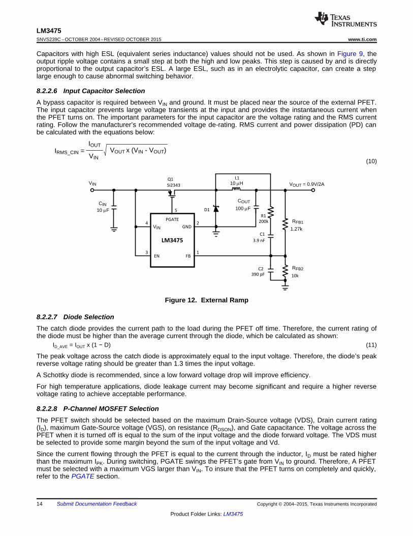
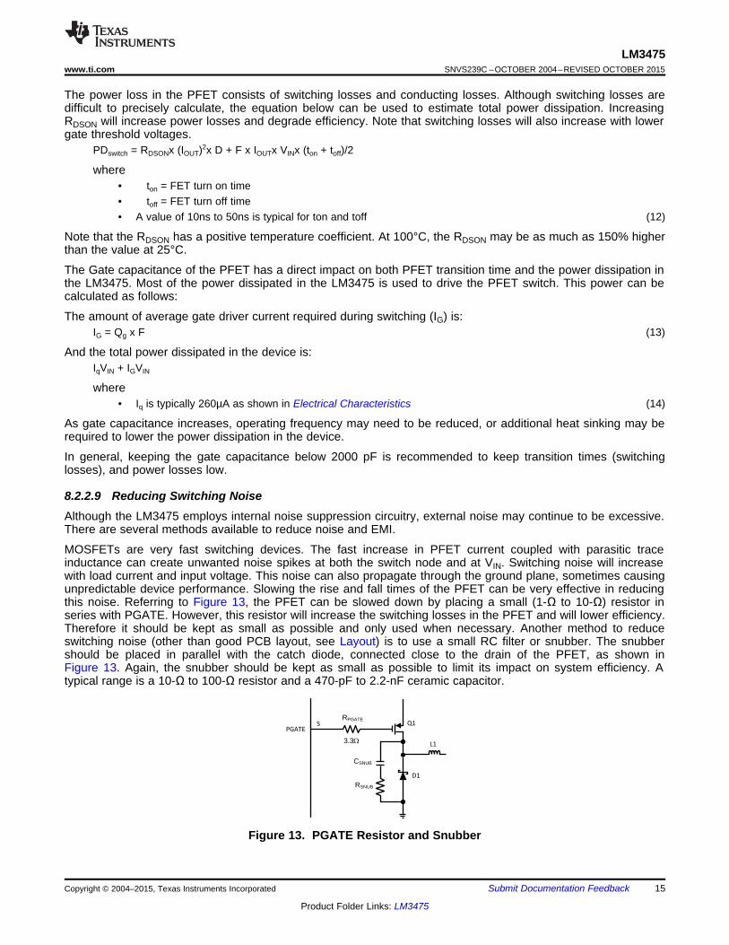
MOSFETs are very fast switching devices. The fast increase in PFET current coupled with parasitic traceinductance can create unwanted noise spikes at both the switch node and at VIN. Switching noise will increasewith load current and input voltage. This noise can also propagate through the ground plane, sometimes causingunpredictable device performance. Slowing the rise and fall times of the PFET can be very effective in reducingthis noise. Referring to Figure 13, the PFET can be slowed down by placing a small (1-Ω to 10-Ω) resistor inseries with PGATE. However, this resistor will increase the switching losses in the PFET and will lower efficiency.Therefore it should be kept as small as possible and only used when necessary. Another method to reduceswitching noise (other than good PCB layout, see Layout) is to use a small RC filter or snubber. The snubbershould be placed in parallel with the catch diode, connected close to the drain of the PFET, as shown inFigure 13. Again, the snubber should be kept as small as possible to limit its impact on system efficiency. Atypical range is a 10-Ω to 100-Ω resistor and a 470-pF to 2.2-nF ceramic capacitor.
Figure 13. PGATE Resistor and Snubber
Copyright © 2004–2015, Texas Instruments Incorporated Submit Documentation Feedback 15
Product Folder Links: LM3475
LM3475SNVS239C –OCTOBER 2004–REVISED OCTOBER 2015 www.ti.com
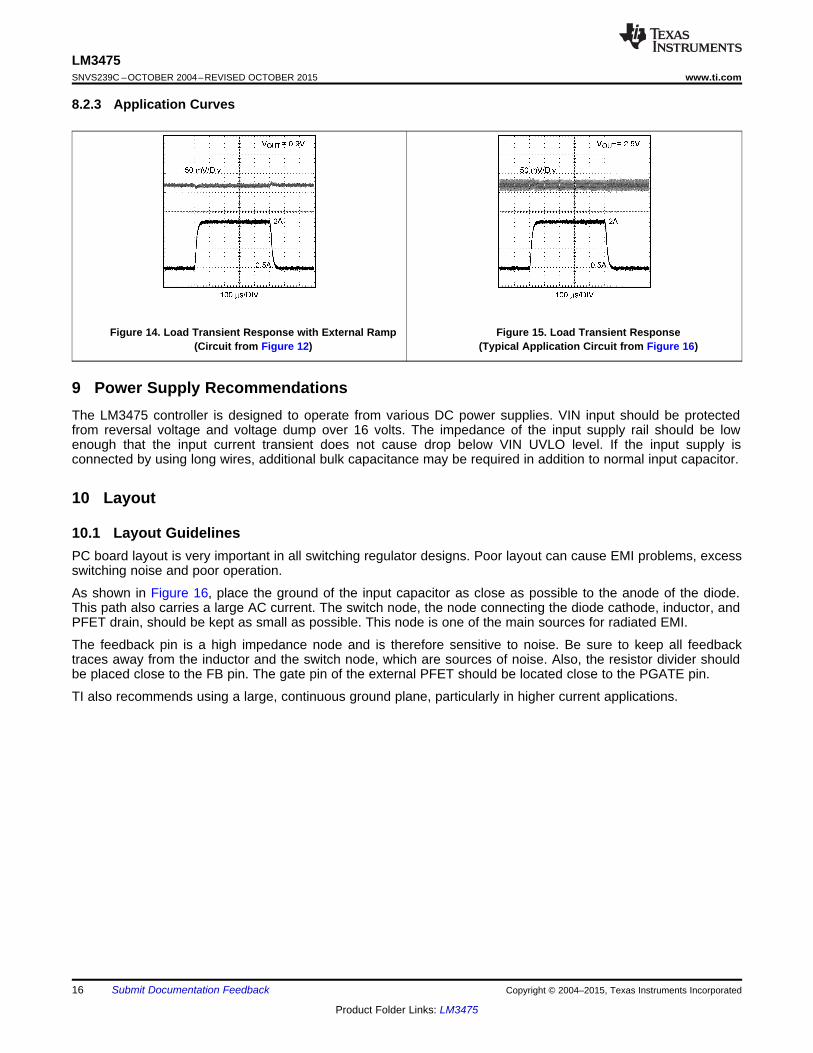
8.2.3 Application Curves
Figure 14. Load Transient Response with External Ramp Figure 15. Load Transient Response(Circuit from Figure 12) (Typical Application Circuit from Figure 16)
9 Power Supply RecommendationsThe LM3475 controller is designed to operate from various DC power supplies. VIN input should be protectedfrom reversal voltage and voltage dump over 16 volts. The impedance of the input supply rail should be lowenough that the input current transient does not cause drop below VIN UVLO level. If the input supply isconnected by using long wires, additional bulk capacitance may be required in addition to normal input capacitor.
10 Layout
10.1 Layout GuidelinesPC board layout is very important in all switching regulator designs. Poor layout can cause EMI problems, excessswitching noise and poor operation.
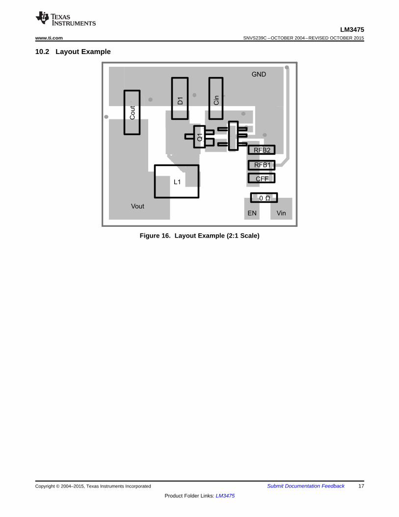
As shown in Figure 16, place the ground of the input capacitor as close as possible to the anode of the diode.This path also carries a large AC current. The switch node, the node connecting the diode cathode, inductor, andPFET drain, should be kept as small as possible. This node is one of the main sources for radiated EMI.
The feedback pin is a high impedance node and is therefore sensitive to noise. Be sure to keep all feedbacktraces away from the inductor and the switch node, which are sources of noise. Also, the resistor divider shouldbe placed close to the FB pin. The gate pin of the external PFET should be located close to the PGATE pin.
TI also recommends using a large, continuous ground plane, particularly in higher current applications.
16 Submit Documentation Feedback Copyright © 2004–2015, Texas Instruments Incorporated
Product Folder Links: LM3475
Cout
L1
Cin
D1
RFB2
CFF
RFB1
0 Ω
GND
Vout
VinEN
Q1
LM3475www.ti.com SNVS239C –OCTOBER 2004–REVISED OCTOBER 2015
10.2 Layout Example
Figure 16. Layout Example (2:1 Scale)
Copyright © 2004–2015, Texas Instruments Incorporated Submit Documentation Feedback 17
Product Folder Links: LM3475
LM3475SNVS239C –OCTOBER 2004–REVISED OCTOBER 2015 www.ti.com
11 Device and Documentation Support
11.1 Device Support
11.1.1 Third-Party Products DisclaimerTI'S PUBLICATION OF INFORMATION REGARDING THIRD-PARTY PRODUCTS OR SERVICES DOES NOTCONSTITUTE AN ENDORSEMENT REGARDING THE SUITABILITY OF SUCH PRODUCTS OR SERVICESOR A WARRANTY, REPRESENTATION OR ENDORSEMENT OF SUCH PRODUCTS OR SERVICES, EITHERALONE OR IN COMBINATION WITH ANY TI PRODUCT OR SERVICE.
11.2 Community ResourcesThe following links connect to TI community resources. Linked contents are provided "AS IS" by the respectivecontributors. They do not constitute TI specifications and do not necessarily reflect TI's views; see TI's Terms ofUse.
TI E2E™ Online Community TI's Engineer-to-Engineer (E2E) Community. Created to foster collaborationamong engineers. At e2e.ti.com, you can ask questions, share knowledge, explore ideas and helpsolve problems with fellow engineers.
Design Support TI's Design Support Quickly find helpful E2E forums along with design support tools andcontact information for technical support.
11.3 TrademarksE2E is a trademark of Texas Instruments.All other trademarks are the property of their respective owners.
11.4 Electrostatic Discharge CautionThese devices have limited built-in ESD protection. The leads should be shorted together or the device placed in conductive foamduring storage or handling to prevent electrostatic damage to the MOS gates.
11.5 GlossarySLYZ022 — TI Glossary.
This glossary lists and explains terms, acronyms, and definitions.
12 Mechanical, Packaging, and Orderable InformationThe following pages include mechanical, packaging, and orderable information. This information is the mostcurrent data available for the designated devices. This data is subject to change without notice and revision ofthis document. For browser-based versions of this data sheet, refer to the left-hand navigation.
18 Submit Documentation Feedback Copyright © 2004–2015, Texas Instruments Incorporated
Product Folder Links: LM3475
PACKAGE OPTION ADDENDUM
www.ti.com 17-Mar-2017
Addendum-Page 1
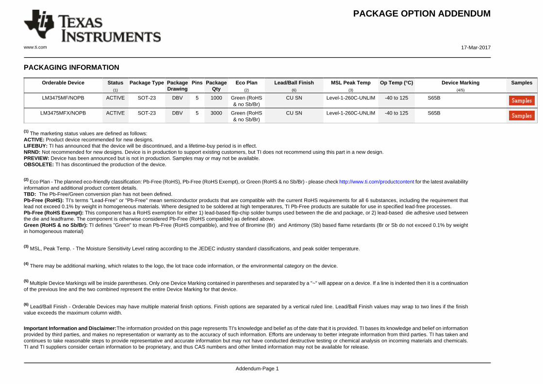
PACKAGING INFORMATION
Orderable Device Status(1)
Package Type PackageDrawing
Pins PackageQty
Eco Plan(2)
Lead/Ball Finish(6)
MSL Peak Temp(3)
Op Temp (°C) Device Marking(4/5)
Samples
LM3475MF/NOPB ACTIVE SOT-23 DBV 5 1000 Green (RoHS& no Sb/Br)
CU SN Level-1-260C-UNLIM -40 to 125 S65B
LM3475MFX/NOPB ACTIVE SOT-23 DBV 5 3000 Green (RoHS& no Sb/Br)
CU SN Level-1-260C-UNLIM -40 to 125 S65B
(1) The marketing status values are defined as follows:ACTIVE: Product device recommended for new designs.LIFEBUY: TI has announced that the device will be discontinued, and a lifetime-buy period is in effect.NRND: Not recommended for new designs. Device is in production to support existing customers, but TI does not recommend using this part in a new design.PREVIEW: Device has been announced but is not in production. Samples may or may not be available.OBSOLETE: TI has discontinued the production of the device.
(2) Eco Plan - The planned eco-friendly classification: Pb-Free (RoHS), Pb-Free (RoHS Exempt), or Green (RoHS & no Sb/Br) - please check http://www.ti.com/productcontent for the latest availabilityinformation and additional product content details.TBD: The Pb-Free/Green conversion plan has not been defined.Pb-Free (RoHS): TI's terms "Lead-Free" or "Pb-Free" mean semiconductor products that are compatible with the current RoHS requirements for all 6 substances, including the requirement thatlead not exceed 0.1% by weight in homogeneous materials. Where designed to be soldered at high temperatures, TI Pb-Free products are suitable for use in specified lead-free processes.Pb-Free (RoHS Exempt): This component has a RoHS exemption for either 1) lead-based flip-chip solder bumps used between the die and package, or 2) lead-based die adhesive used betweenthe die and leadframe. The component is otherwise considered Pb-Free (RoHS compatible) as defined above.Green (RoHS & no Sb/Br): TI defines "Green" to mean Pb-Free (RoHS compatible), and free of Bromine (Br) and Antimony (Sb) based flame retardants (Br or Sb do not exceed 0.1% by weightin homogeneous material)
(3) MSL, Peak Temp. - The Moisture Sensitivity Level rating according to the JEDEC industry standard classifications, and peak solder temperature.
(4) There may be additional marking, which relates to the logo, the lot trace code information, or the environmental category on the device.
(5) Multiple Device Markings will be inside parentheses. Only one Device Marking contained in parentheses and separated by a "~" will appear on a device. If a line is indented then it is a continuationof the previous line and the two combined represent the entire Device Marking for that device.
(6) Lead/Ball Finish - Orderable Devices may have multiple material finish options. Finish options are separated by a vertical ruled line. Lead/Ball Finish values may wrap to two lines if the finishvalue exceeds the maximum column width.
Important Information and Disclaimer:The information provided on this page represents TI's knowledge and belief as of the date that it is provided. TI bases its knowledge and belief on informationprovided by third parties, and makes no representation or warranty as to the accuracy of such information. Efforts are underway to better integrate information from third parties. TI has taken andcontinues to take reasonable steps to provide representative and accurate information but may not have conducted destructive testing or chemical analysis on incoming materials and chemicals.TI and TI suppliers consider certain information to be proprietary, and thus CAS numbers and other limited information may not be available for release.
PACKAGE OPTION ADDENDUM
www.ti.com 17-Mar-2017
Addendum-Page 2
In no event shall TI's liability arising out of such information exceed the total purchase price of the TI part(s) at issue in this document sold by TI to Customer on an annual basis.
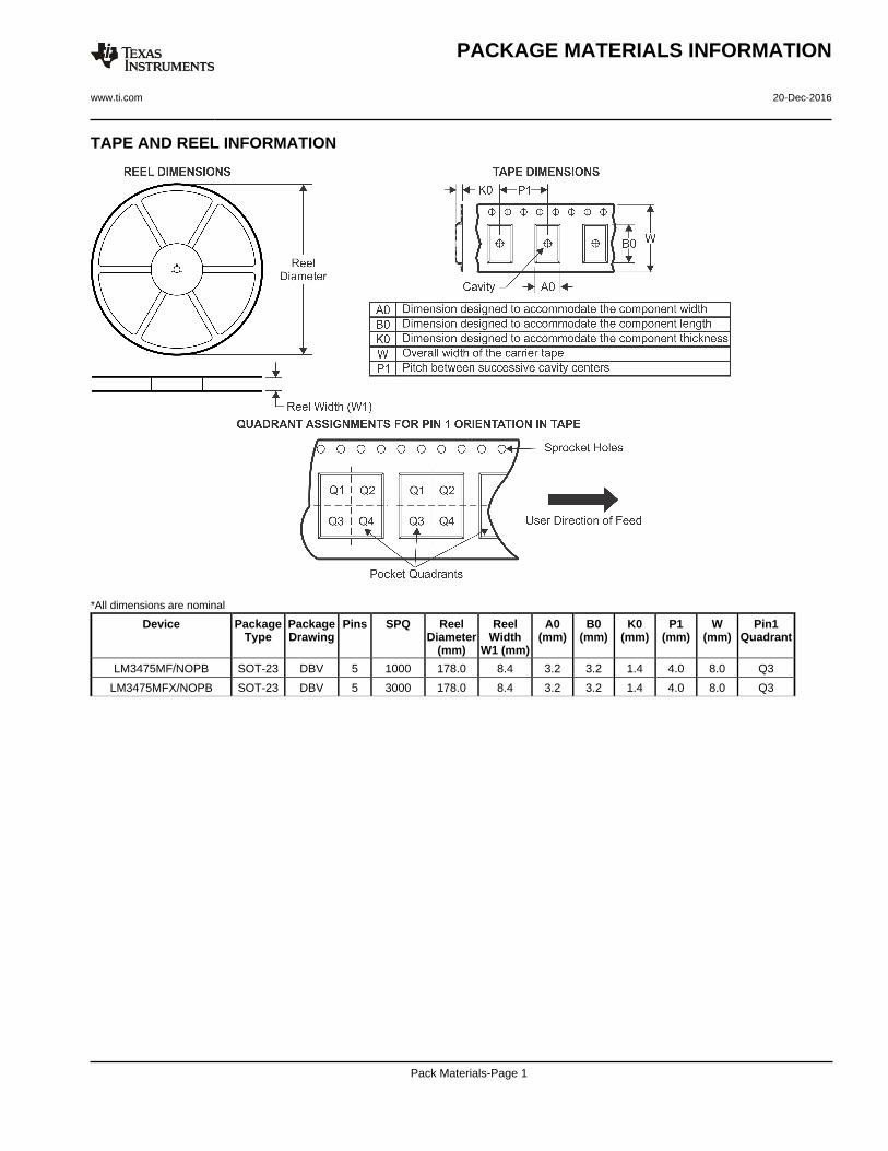
TAPE AND REEL INFORMATION
*All dimensions are nominal
Device PackageType
PackageDrawing
Pins SPQ ReelDiameter
(mm)
ReelWidth
W1 (mm)
A0(mm)
B0(mm)
K0(mm)
P1(mm)
W(mm)
Pin1Quadrant
LM3475MF/NOPB SOT-23 DBV 5 1000 178.0 8.4 3.2 3.2 1.4 4.0 8.0 Q3
LM3475MFX/NOPB SOT-23 DBV 5 3000 178.0 8.4 3.2 3.2 1.4 4.0 8.0 Q3
PACKAGE MATERIALS INFORMATION
www.ti.com 20-Dec-2016
Pack Materials-Page 1
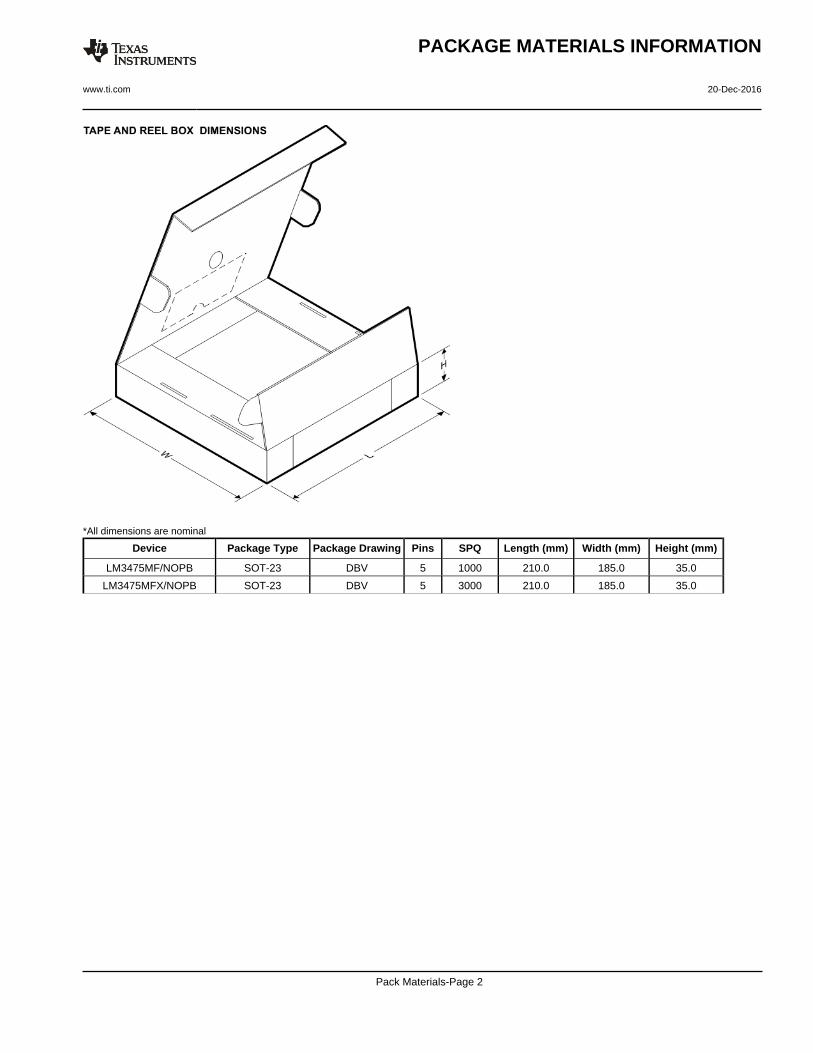
*All dimensions are nominal
Device Package Type Package Drawing Pins SPQ Length (mm) Width (mm) Height (mm)
LM3475MF/NOPB SOT-23 DBV 5 1000 210.0 185.0 35.0
LM3475MFX/NOPB SOT-23 DBV 5 3000 210.0 185.0 35.0
PACKAGE MATERIALS INFORMATION
www.ti.com 20-Dec-2016
Pack Materials-Page 2

www.ti.com
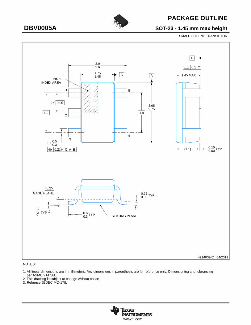
PACKAGE OUTLINE
C
TYP0.220.08
0.25
3.02.6
2X 0.95
1.9
1.45 MAX
TYP0.150.00
5X 0.50.3
TYP0.60.3
TYP80
1.9
A
3.052.75
B1.751.45
(1.1)
SOT-23 - 1.45 mm max heightDBV0005ASMALL OUTLINE TRANSISTOR
4214839/C 04/2017
NOTES: 1. All linear dimensions are in millimeters. Any dimensions in parenthesis are for reference only. Dimensioning and tolerancing per ASME Y14.5M.2. This drawing is subject to change without notice.3. Refernce JEDEC MO-178.
0.2 C A B
1
34
5
2
INDEX AREAPIN 1
GAGE PLANE
SEATING PLANE
0.1 C
SCALE 4.000

www.ti.com
EXAMPLE BOARD LAYOUT
0.07 MAXARROUND
0.07 MINARROUND
5X (1.1)
5X (0.6)
(2.6)
(1.9)
2X (0.95)
(R0.05) TYP
4214839/C 04/2017
SOT-23 - 1.45 mm max heightDBV0005ASMALL OUTLINE TRANSISTOR
NOTES: (continued) 4. Publication IPC-7351 may have alternate designs. 5. Solder mask tolerances between and around signal pads can vary based on board fabrication site.
SYMM
LAND PATTERN EXAMPLEEXPOSED METAL SHOWN
SCALE:15X
PKG
1
3 4
5
2
SOLDER MASKOPENINGMETAL UNDER
SOLDER MASK
SOLDER MASKDEFINED
EXPOSED METAL
METALSOLDER MASKOPENING
NON SOLDER MASKDEFINED
(PREFERRED)
SOLDER MASK DETAILS
EXPOSED METAL

www.ti.com
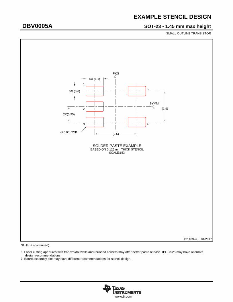
EXAMPLE STENCIL DESIGN
(2.6)
(1.9)
2X(0.95)
5X (1.1)
5X (0.6)
(R0.05) TYP
SOT-23 - 1.45 mm max heightDBV0005ASMALL OUTLINE TRANSISTOR
4214839/C 04/2017
NOTES: (continued) 6. Laser cutting apertures with trapezoidal walls and rounded corners may offer better paste release. IPC-7525 may have alternate design recommendations. 7. Board assembly site may have different recommendations for stencil design.
SOLDER PASTE EXAMPLEBASED ON 0.125 mm THICK STENCIL
SCALE:15X
SYMM
PKG
1
3 4
5
2
www.ti.com
PACKAGE OUTLINE
C
TYP0.220.08
0.25
3.02.6
2X 0.95
1.9
1.45 MAX
TYP0.150.00
5X 0.50.3
TYP0.60.3
TYP80
1.9
A
3.052.75
B1.751.45
(1.1)
SOT-23 - 1.45 mm max heightDBV0005ASMALL OUTLINE TRANSISTOR
4214839/C 04/2017
NOTES: 1. All linear dimensions are in millimeters. Any dimensions in parenthesis are for reference only. Dimensioning and tolerancing per ASME Y14.5M.2. This drawing is subject to change without notice.3. Refernce JEDEC MO-178.
0.2 C A B
1
34
5
2
INDEX AREAPIN 1
GAGE PLANE
SEATING PLANE
0.1 C
SCALE 4.000
www.ti.com
EXAMPLE BOARD LAYOUT
0.07 MAXARROUND
0.07 MINARROUND
5X (1.1)
5X (0.6)
(2.6)
(1.9)
2X (0.95)
(R0.05) TYP
4214839/C 04/2017
SOT-23 - 1.45 mm max heightDBV0005ASMALL OUTLINE TRANSISTOR
NOTES: (continued) 4. Publication IPC-7351 may have alternate designs. 5. Solder mask tolerances between and around signal pads can vary based on board fabrication site.
SYMM
LAND PATTERN EXAMPLEEXPOSED METAL SHOWN
SCALE:15X
PKG
1
3 4
5
2
SOLDER MASKOPENINGMETAL UNDER
SOLDER MASK
SOLDER MASKDEFINED
EXPOSED METAL
METALSOLDER MASKOPENING
NON SOLDER MASKDEFINED
(PREFERRED)
SOLDER MASK DETAILS
EXPOSED METAL
www.ti.com
EXAMPLE STENCIL DESIGN
(2.6)
(1.9)
2X(0.95)
5X (1.1)
5X (0.6)
(R0.05) TYP
SOT-23 - 1.45 mm max heightDBV0005ASMALL OUTLINE TRANSISTOR
4214839/C 04/2017
NOTES: (continued) 6. Laser cutting apertures with trapezoidal walls and rounded corners may offer better paste release. IPC-7525 may have alternate design recommendations. 7. Board assembly site may have different recommendations for stencil design.
SOLDER PASTE EXAMPLEBASED ON 0.125 mm THICK STENCIL
SCALE:15X
SYMM
PKG
1
3 4
5
2
IMPORTANT NOTICE
Texas Instruments Incorporated (TI) reserves the right to make corrections, enhancements, improvements and other changes to itssemiconductor products and services per JESD46, latest issue, and to discontinue any product or service per JESD48, latest issue. Buyersshould obtain the latest relevant information before placing orders and should verify that such information is current and complete.TI’s published terms of sale for semiconductor products (http://www.ti.com/sc/docs/stdterms.htm) apply to the sale of packaged integratedcircuit products that TI has qualified and released to market. Additional terms may apply to the use or sale of other types of TI products andservices.Reproduction of significant portions of TI information in TI data sheets is permissible only if reproduction is without alteration and isaccompanied by all associated warranties, conditions, limitations, and notices. TI is not responsible or liable for such reproduceddocumentation. Information of third parties may be subject to additional restrictions. Resale of TI products or services with statementsdifferent from or beyond the parameters stated by TI for that product or service voids all express and any implied warranties for theassociated TI product or service and is an unfair and deceptive business practice. TI is not responsible or liable for any such statements.Buyers and others who are developing systems that incorporate TI products (collectively, “Designers”) understand and agree that Designersremain responsible for using their independent analysis, evaluation and judgment in designing their applications and that Designers havefull and exclusive responsibility to assure the safety of Designers' applications and compliance of their applications (and of all TI productsused in or for Designers’ applications) with all applicable regulations, laws and other applicable requirements. Designer represents that, withrespect to their applications, Designer has all the necessary expertise to create and implement safeguards that (1) anticipate dangerousconsequences of failures, (2) monitor failures and their consequences, and (3) lessen the likelihood of failures that might cause harm andtake appropriate actions. Designer agrees that prior to using or distributing any applications that include TI products, Designer willthoroughly test such applications and the functionality of such TI products as used in such applications.TI’s provision of technical, application or other design advice, quality characterization, reliability data or other services or information,including, but not limited to, reference designs and materials relating to evaluation modules, (collectively, “TI Resources”) are intended toassist designers who are developing applications that incorporate TI products; by downloading, accessing or using TI Resources in anyway, Designer (individually or, if Designer is acting on behalf of a company, Designer’s company) agrees to use any particular TI Resourcesolely for this purpose and subject to the terms of this Notice.TI’s provision of TI Resources does not expand or otherwise alter TI’s applicable published warranties or warranty disclaimers for TIproducts, and no additional obligations or liabilities arise from TI providing such TI Resources. TI reserves the right to make corrections,enhancements, improvements and other changes to its TI Resources. TI has not conducted any testing other than that specificallydescribed in the published documentation for a particular TI Resource.Designer is authorized to use, copy and modify any individual TI Resource only in connection with the development of applications thatinclude the TI product(s) identified in such TI Resource. NO OTHER LICENSE, EXPRESS OR IMPLIED, BY ESTOPPEL OR OTHERWISETO ANY OTHER TI INTELLECTUAL PROPERTY RIGHT, AND NO LICENSE TO ANY TECHNOLOGY OR INTELLECTUAL PROPERTYRIGHT OF TI OR ANY THIRD PARTY IS GRANTED HEREIN, including but not limited to any patent right, copyright, mask work right, orother intellectual property right relating to any combination, machine, or process in which TI products or services are used. Informationregarding or referencing third-party products or services does not constitute a license to use such products or services, or a warranty orendorsement thereof. Use of TI Resources may require a license from a third party under the patents or other intellectual property of thethird party, or a license from TI under the patents or other intellectual property of TI.TI RESOURCES ARE PROVIDED “AS IS” AND WITH ALL FAULTS. TI DISCLAIMS ALL OTHER WARRANTIES ORREPRESENTATIONS, EXPRESS OR IMPLIED, REGARDING RESOURCES OR USE THEREOF, INCLUDING BUT NOT LIMITED TOACCURACY OR COMPLETENESS, TITLE, ANY EPIDEMIC FAILURE WARRANTY AND ANY IMPLIED WARRANTIES OFMERCHANTABILITY, FITNESS FOR A PARTICULAR PURPOSE, AND NON-INFRINGEMENT OF ANY THIRD PARTY INTELLECTUALPROPERTY RIGHTS. TI SHALL NOT BE LIABLE FOR AND SHALL NOT DEFEND OR INDEMNIFY DESIGNER AGAINST ANY CLAIM,INCLUDING BUT NOT LIMITED TO ANY INFRINGEMENT CLAIM THAT RELATES TO OR IS BASED ON ANY COMBINATION OFPRODUCTS EVEN IF DESCRIBED IN TI RESOURCES OR OTHERWISE. IN NO EVENT SHALL TI BE LIABLE FOR ANY ACTUAL,DIRECT, SPECIAL, COLLATERAL, INDIRECT, PUNITIVE, INCIDENTAL, CONSEQUENTIAL OR EXEMPLARY DAMAGES INCONNECTION WITH OR ARISING OUT OF TI RESOURCES OR USE THEREOF, AND REGARDLESS OF WHETHER TI HAS BEENADVISED OF THE POSSIBILITY OF SUCH DAMAGES.Unless TI has explicitly designated an individual product as meeting the requirements of a particular industry standard (e.g., ISO/TS 16949and ISO 26262), TI is not responsible for any failure to meet such industry standard requirements.Where TI specifically promotes products as facilitating functional safety or as compliant with industry functional safety standards, suchproducts are intended to help enable customers to design and create their own applications that meet applicable functional safety standardsand requirements. Using products in an application does not by itself establish any safety features in the application. Designers mustensure compliance with safety-related requirements and standards applicable to their applications. Designer may not use any TI products inlife-critical medical equipment unless authorized officers of the parties have executed a special contract specifically governing such use.Life-critical medical equipment is medical equipment where failure of such equipment would cause serious bodily injury or death (e.g., lifesupport, pacemakers, defibrillators, heart pumps, neurostimulators, and implantables). Such equipment includes, without limitation, allmedical devices identified by the U.S. Food and Drug Administration as Class III devices and equivalent classifications outside the U.S.TI may expressly designate certain products as completing a particular qualification (e.g., Q100, Military Grade, or Enhanced Product).Designers agree that it has the necessary expertise to select the product with the appropriate qualification designation for their applicationsand that proper product selection is at Designers’ own risk. Designers are solely responsible for compliance with all legal and regulatoryrequirements in connection with such selection.Designer will fully indemnify TI and its representatives against any damages, costs, losses, and/or liabilities arising out of Designer’s non-compliance with the terms and provisions of this Notice.
Mailing Address: Texas Instruments, Post Office Box 655303, Dallas, Texas 75265Copyright © 2018, Texas Instruments Incorporated