Embed Size (px)
Citation preview

MODEL NO. PAGE
DET090WVNTCMI-1A SPEC & SAMPLE 1
DENSITRON® DISPLAYS
LIQUID CRYSTAL DISPLAY MODULE
Product Specification
CUSTOMER Standard
CUSTOMER
PART NUMBER
PRODUCT
NUMBER DET090WVNTCMI-1W
Product Mgr Design Eng
Bruno Recaldini Luo Luo
Date: 07-March-13 Date: 07-March-13
Approval for Specification only
Approval for Specification and Sample

MODEL NO. PAGE
DET090WVNTCMI-1A SPEC & SAMPLE 2
DENSITRON® DISPLAYS
1. Table of Contents
No. Contents Page
1 Table of Contents 2
2 Record of Revisions 3
3 Module Numbering System 4
4 Application 5
5 Features 5
6 General Specifications 5
7 Absolute Maximum Ratings 6
8 Electrical Characteristics 7
9 Block Diagram 9
10 Input / Output Terminals Pin Assignment 10
11 Interface Timing 15
12 Optical Characteristics 25
13 Reliability Test 28
14 Packaging 29
15 Precautions 30
16 Outline Drawing 31
17 Incoming Inspection Standards 32

MODEL NO. PAGE
DET090WVNTCMI-1A SPEC & SAMPLE 3
DENSITRON® DISPLAYS
2. Record of Revisions
Rev. Comments Page Date
1 Preliminary Specification was first issued. All 07/0313

MODEL NO. PAGE
DET090WVNTCMI-1A SPEC & SAMPLE 4
DENSITRON® DISPLAYS
3. Module Numbering System
1 2 3 4 5 6 7 8 9 10 11 12 13 14 15 16
D E T 0 9 0 W V N T C M I - 1 A
1 D
DENSITRON Standard TFT 2 E
3 T
4~6
0 TFT Size:
043=4.3'', 057=5.7'', 070=7'', 090=9'', 101=10.1'' 9
0
7~8
W TFT Resolution:
QQ: 480X272 (Quarter VGA), VG: 640X480 (VGA)
WV: 800X480 (WVGA), WS: 1024X600 (WSVGA) V
9 N TFT Brightness:
N: Normal Brightness, H: High Brightness
10 T TFT Interface System:
T: TTL, L: LVDS
11~13
C Touch Type:
NT: Non-Touch, CS: Capacitive Single Touch,
CM: Capacitive Multi Touch, RS: Resistive Single Touch, RM:
Resistive Multi Touch M
I Touch Interface:
0: No interface, U: USB I/F, I: I2C I/F, S: SPI I/F
14 -
15~16 1 Revision
A A: Standard, W: Wide Viewing Angle

MODEL NO. PAGE
DET090WVNTCMI-1A SPEC & SAMPLE 5
DENSITRON® DISPLAYS
4. Application
This specification is applied to the 9 inch WVGA supported TFT-LCD module With
projected capacitive touch (PCT) and can display true 262,144 colors (8 bit/ color).
The module is designed for OA, Car TV application and other electronic products
which require flat panel display of digital signal interface. This module is composed
of a 9” TFT-LCD panel, a driver circuit and LED backlight unit and used as the input
devices for general electric appliances via human’s finger.
5. Features
- WVGA (800×480 pixels) resolution.
- Digital 24 bit parallel RGB.
- Dot inversion mode with stripe type.
- Projected Capacitive Touch
I2C Interface
Multi Touch (Ten points)
6. General Specifications
Item Specifications Unit
Screen Size 9 (Diagonal) inch
Display Format 800RGB(H)×480(V) dot
Active Area 198.0(H)×111.696(V) mm
Dot Pitch 0.0825(H)×0.2327(V) mm
Pixel Configuration RGB Vertical Stripe -
Display Mode
TN Type
Transmissive Mode
Normally White
-
Surface Treatment Clear(7H)
-
Viewing Direction 6 O’clock
(The Gray Inversion will appear at this direction)
-
Outline Dimension 211.1(W)×126.5(H)×7.45(D) mm
Weight 343 g
RoHS Compliance
DNSITRON certifies this product to be in
compliance with European Union Directive
2002/95/EC on the restriction of certain
hazardous substances in electrical and electronic
equipment.
-

MODEL NO. PAGE
DET090WVNTCMI-1A SPEC & SAMPLE 6
DENSITRON® DISPLAYS
7. Absolute Maximum Ratings
7.1 Absolute Ratings of Environment
Item Symbol Value
Unit Note Min. Max.
Storage Temperature TST -30 +80 °C (1)(2)
Operating Ambient Temperature TOP -20 +70 °C (1)(2)
Note1: Background color changes slightly depending on ambient temperature.
This phenomenon is reversible.
Note2: Please refer to item of RELIABILITY.
7.2 Electrical Absolute Ratings
7.2.1 TFT-LCD Module
(Ta=25±2°C, GND=VSS=0V)
Item Symbol Value
Unit Note Min. Max.
Digital Power Supply Voltage DVDD -0.3 5.0 V -
Analog Power Supply Voltage AVDD -0.5 13.5 V -
Gate High Voltage VGH 13.0 19.0 V -
Gate Low Voltage VGL -12.0 -2.0 V -
Gate High To Gate Low Voltage VGH - VGL - 31.0 V -
7.2.2 Backlight Unit
(Ta=25±2°C)
Item Symbol Value
Unit Note Min. Max.
Current of Backlight Unit IB - 250 mA (1)
Voltage of Backlight Unit VB - 11.0 V (1)
Note (1) Permanent damage to the device may occur if maximum values are
exceeded or reverse voltage is loaded.

MODEL NO. PAGE
DET090WVNTCMI-1A SPEC & SAMPLE 7
DENSITRON® DISPLAYS
8. Electrical Characteristics
8.1 TFT-LCD Module
(Ta=25±2°C)
Item Symbol Value
Unit Note Min. Typ. Max.
Digital Power Supply Voltage DVDD 3.0 3.3 3.6 V -
Analog Power Supply Voltage AVDD 10.2 10.4 10.6 V -
Gate High Voltage VGH 16.3 17.0 17.7 V -
Gate Low Voltage VGL -5.7 -5.0 -4.3 V -
Input signal voltage VCOM 4.0 4.2 4.4 V -
Digital Power Supply Current DIDD - 5.5 10 mA (1)
Analog Power Supply Current AIDD 32 50 mA (1)
Gate High Current IGH 0.3 1 mA (1)
Gate Low Current IGL 0.3 1 mA (1)
Input High Threshold Voltage VIH 0.7 DVDD - DVDD V -
Input Low Threshold Voltage VIL 0 - 0.3 DVDD V -
VSYNC Frequency FV - 60 - Hz -
DCLK Frequency DCLK - 33.26 - MHz -
Note (1) The specified power consumption is under the conditions at DVDD =3.3V, AVDD
=10.4V, VGH =17.0V, VGL =-5V, VCOM =4.2V ,FV=60Hz, whereas a power dissipation
check pattern below is displayed.
Active Area
Black Pattern / 0 Gray

MODEL NO. PAGE
DET090WVNTCMI-1A SPEC & SAMPLE 8
DENSITRON® DISPLAYS
8.2 Backlight Unit (Ta=25±2°C)
Item Symbol Value
Unit Note Min. Typ. Max.
Current of Backlight Unit IB 198 220 242 mA (1)
Voltage of Backlight Unit VB 9.3 9.9 10.5 V IB =220mA
Power Consumption PBL - (2.18) - W IB =220mA
LED Life Time(25℃) - 20000 - - hr (2)
Note 1: The LED Supply Voltage is defined by the number of LED at Ta=25℃ and
IL =220mA.
Note 2: The “LED life time” is defined as the module brightness decrease to 50% original
brightness at Ta=25℃ and IL =220mA. The LED lifetime could be decreased if
operating IL is lager than 220 mA.
8.3 Projected Capacitive Touch
Item Value
Unit Note Min. Typ. Max.
Operating Voltage 3.0 3.3 3.6 V -
Power Supply Current - 16.6 23.3 mA (1)
Power Consumption - 54.78 76.89 mW @3.3V
Interface I2C -
Function Multi Touch -
Note (1) This test condition is touched with 10 points.

MODEL NO. PAGE
DET090WVNTCMI-1A SPEC & SAMPLE 9
DENSITRON® DISPLAYS
9. Block Diagram
9.1 TFT-LCD Module with Backlight Unit
TFT LCD PANEL
800 x (RGB) x 480
Pixel
VLED
GLED
GND
VCOM
DVDD
MODE
DE
VS
HS
R0~R7
G0~G7
B0~B7
DCLK
L/R
U/D
VGH
VGL
AVDD
RESET
DITHB
So
urc
e d
rive
r with
bu
ild-in
Tim
ing
Co
ntro
ller
Ga
te d
rive
r
888
B/L
GND
VDD
/RST
/INT
SDA
SCL
NC
NC
NC
GND
Projected Capacitive Touch

MODEL NO. PAGE
DET090WVNTCMI-1A SPEC & SAMPLE 10
DENSITRON® DISPLAYS
10. Input / Output Terminals Pin Assignment
10.1 TFT-LCD Module
Connector: Hirose FH12A-50S-0.5SH
Pin No. Symbol I/O Description Remark
1 VLED - Power for LED backlight
2 VLED - Power for LED backlight
3 GLED - Ground for LED backlight
4 GLED - Ground for LED backlight
5 GND P Ground
6 VCOM I Common voltage
7 DVDD P Power for Digital Circuit
8 MODE I DE/SYNC mode select Note 1
9 DE I Data Input Enable
10 VS I Vertical Sync Input
11 HS I Horizontal Sync Input
12 B7 I Blue data(MSB)
13 B6 I Blue data
14 B5 I Blue data
15 B4 I Blue data
16 B3 I Blue data
17 B4 I Blue data
18 B1 I Blue data Note 2
19 B0 I Blue data(LSB) Note 2
20 G7 I GREEN data(MSB)
21 G6 I GREEN data
22 G5 I GREEN data
23 G4 I GREEN data
24 G3 I GREEN data
25 G2 I GREEN data
26 G1 I GREEN data Note 2
27 G0 I GREEN data(LSB) Note 2
28 R7 I RED data(MSB)
29 R6 I RED data
30 R5 I RED data

MODEL NO. PAGE
DET090WVNTCMI-1A SPEC & SAMPLE 11
DENSITRON® DISPLAYS
Pin No. Symbol I/O Description Remark
31 R4 I RED data
32 R3 I RED data
33 R2 I RED data
34 R1 I RED data Note 2
35 R0 I RED data (LSB) Note 2
36 GND P Ground
37 DCLK I Sample clock Note 3
38 GND P Ground
39 L/R I Left / right selection Note 4,5
40 U/D I Up / down selection Note 4,5
41 VGH P Gate ON Voltage
42 VGL P Gate OFF Voltage
43 AVDD P Power for Analog Circuit
44 RESET I Global reset pin. Note 6
45 NC - No connection
46 VCOM I Common Voltage
47 DITHB I Dithering function Note 7
48 GND P Ground
49 NC - No connection
50 NC - No connection
I: input, O: output, P: Power
Note 1: DE/SYNC mode select. Normally pull high.
When select DE mode, MODE=”1”, VS and HS must pull high.
When select SYNC mode, MODE= ”0”, DE must be grounded.
Note 2: When input 18 bits RGB data, the two low bits of R, G and B data must be grounded.
Note 3: Data shall be latched at the falling edge of DCLK.
Note 4: Selection of scanning mode
Note 5: Definition of scanning direction.

MODEL NO. PAGE
DET090WVNTCMI-1A SPEC & SAMPLE 12
DENSITRON® DISPLAYS
Refer to the figure as below:
Note 6: Global reset pin. Active low to enter reset state. Suggest to connect with an RC reset circuit for
stability. Normally pull high.
Note 7: Dithering function enable control, normally pull high.
When DITHB=”1”,Disable internal dithering function,
When DITHB=”0”,Enable internal dithering function,

MODEL NO. PAGE
DET090WVNTCMI-1A SPEC & SAMPLE 13
DENSITRON® DISPLAYS
10.2 Projected Capacitive Touch
Connector: CVILUX CF25101D0R0-05
Pin No. Symbol I/O Description
1 GND I System ground.
2 VDD I +3.3V power supply.
3 /RST I External reset signal, active low.
4 /INT O Interrupt signal, active low, asserted to request Host start a new transcation.
5 SDA I/O I2C data signal.
6 SCL I I2C clock signal.
7 NC - Not Connection
8 NC - Not Connection
9 NC - Not Connection
10 GND I System ground.

MODEL NO. PAGE
DET090WVNTCMI-1A SPEC & SAMPLE 14
DENSITRON® DISPLAYS
10.3 Color Data Input Assignment
The brightness of each primary color(red, green and blue) is based on the
8 bit gray scale data input for the color. The higher the binary input, the brighter
the color. The table provides the assignment of color versus data input.
Color
Data Signal
Red Green Blue
R7 R6 R5 R4 R3 R2 R1 R0 G7 G6 G5 G4 G3 G2 G1 G0 B7 B6 B5 B4 B3 B2 B1 B0
Basic Colors
Black 0 0 0 0 0 0 0 0 0 0 0 0 0 0 0 0 0 0 0 0 0 0 0 0
Red 1 1 1 1 1 1 1 1 0 0 0 0 0 0 0 0 0 0 0 0 0 0 0 0
Green 0 0 0 0 0 0 0 0 1 1 1 1 1 1 1 1 0 0 0 0 0 0 0 0
Blue 0 0 0 0 0 0 0 0 0 0 0 0 0 0 0 0 1 1 1 1 1 1 1 1
Cyan 0 0 0 0 0 0 0 0 1 1 1 1 1 1 1 1 1 1 1 1 1 1 1 1
Magenta 1 1 1 1 1 1 1 1 0 0 0 0 0 0 0 0 1 1 1 1 1 1 1 1
Yellow 1 1 1 1 1 1 1 1 1 1 1 1 1 1 1 1 0 0 0 0 0 0 0 0
White 1 1 1 1 1 1 1 1 1 1 1 1 1 1 1 1 1 1 1 1 1 1 1 1
Gray Scale Of RED
Red(0) / Dark
0 0 0 0 0 0 0 0 0 0 0 0 0 0 0 0 0 0 0 0 0 0 0 0
Red(1) 0 0 0 0 0 0 0 1 0 0 0 0 0 0 0 0 0 0 0 0 0 0 0 0
Red(2) 0 0 0 0 0 0 1 0 0 0 0 0 0 0 0 0 0 0 0 0 0 0 0 0
: : : : : : : : : : : : : : : : : : : : : : : : :
: : : : : : : : : : : : : : : : : : : : : : : : :
Red(253) 1 1 1 1 1 1 0 1 0 0 0 0 0 0 0 0 0 0 0 0 0 0 0 0
Red(254) 1 1 1 1 1 1 1 0 0 0 0 0 0 0 0 0 0 0 0 0 0 0 0 0
Red(255) 1 1 1 1 1 1 1 1 0 0 0 0 0 0 0 0 0 0 0 0 0 0 0 0
Gray Scale Of Green
Green(0) / Dark
0 0 0 0 0 0 0 0 0 0 0 0 0 0 0 0 0 0 0 0 0 0 0 0
Green(1) 0 0 0 0 0 0 0 0 0 0 0 0 0 0 0 1 0 0 0 0 0 0 0 0
Green(2) 0 0 0 0 0 0 0 0 0 0 0 0 0 0 1 0 0 0 0 0 0 0 0 0
: : : : : : : : : : : : : : : : : : : : : : : : :
: : : : : : : : : : : : : : : : : : : : : : : : :
Green(253) 0 0 0 0 0 0 0 0 1 1 1 1 1 1 0 1 0 0 0 0 0 0 0 0
Green(254) 0 0 0 0 0 0 0 0 1 1 1 1 1 1 1 0 0 0 0 0 0 0 0 0
Green(255) 0 0 0 0 0 0 0 0 1 1 1 1 1 1 1 1 0 0 0 0 0 0 0 0
Gray Scale Of Blue
Blue(0) / Dark
0 0 0 0 0 0 0 0 0 0 0 0 0 0 0 0 0 0 0 0 0 0 0 0
Blue(1) 0 0 0 0 0 0 0 0 0 0 0 0 0 0 0 0 0 0 0 0 0 0 0 1
Blue(2) 0 0 0 0 0 0 0 0 0 0 0 0 0 0 0 0 0 0 0 0 0 0 1 0
: : : : : : : : : : : : : : : : : : : : : : : : :
: : : : : : : : : : : : : : : : : : : : : : : : :
Blue(253) 0 0 0 0 0 0 0 0 0 0 0 0 0 0 0 0 1 1 1 1 1 1 0 1
Blue(254) 0 0 0 0 0 0 0 0 0 0 0 0 0 0 0 0 1 1 1 1 1 1 1 0
Blue(255) 0 0 0 0 0 0 0 0 0 0 0 0 0 0 0 0 1 1 1 1 1 1 1 1

MODEL NO. PAGE
DET090WVNTCMI-1A SPEC & SAMPLE 15
DENSITRON® DISPLAYS
11. Interface Timing
11.1 Input Signal Characteristics

MODEL NO. PAGE
DET090WVNTCMI-1A SPEC & SAMPLE 16
DENSITRON® DISPLAYS
11.2 Power Sequence
Power on:
Power off:

MODEL NO. PAGE
DET090WVNTCMI-1A SPEC & SAMPLE 17
DENSITRON® DISPLAYS
11.3 Timing

MODEL NO. PAGE
DET090WVNTCMI-1A SPEC & SAMPLE 18
DENSITRON® DISPLAYS
11.4 Waveform
11.4.1 Data input format

MODEL NO. PAGE
DET090WVNTCMI-1A SPEC & SAMPLE 19
DENSITRON® DISPLAYS
11.5 Timing Requirement of Projected Capacitive Touch
11.5.1 I2C Data Transfer Format
Mnemonics Description
S I2C Start or I2C Restart
A[6:0] Slave Address = 0x70
W 1’b0: Write
R 1’b1: Read
C ACK
P
STOP: the indicate the end of a packet (if this bit is missing, S will
indicate the end of the current packet and the beginning of the
next packet)
Write N bytes to I2C slave
SA
6
A
5
A
4
A
3
A
2
A
1
A
0
R
WA
R
6
R
5
R
4
R
3
R
2
R
1
R
0A
R
7
D
6
D
5
D
4
D
3
D
2
D
1
D
0A
D
7…
D
6
D
5
D
4
D
3
D
2
D
1
D
0A
D
7P
Slave Addr Data Address[X] Data [X] Data [X+N-1]
STA
RT
WR
ITE
AC
K
AC
K
AC
K
AC
K
STO
P
Set Data Address
SA
6
A
5
A
4
A
3
A
2
A
1
A
0
R
WA
R
6
R
5
R
4
R
3
R
2
R
1
R
0A
R
7P
Slave Addr Data Address[X]
STAR
T
WR
ITE
AC
K
AC
K
STOP
Read X bytes from I2C Slave
SA
6
A
5
A
4
A
3
A
2
A
1
A
0
R
WA
D
6
D
5
D
4
D
3
D
2
D
1
D
0A
D
7…
D
6
D
5
D
4
D
3
D
2
D
1
D
0A
D
7P
Slave Addr Data [N] Data [X+N-1]
STA
RT
Read
AC
K
AC
K
AC
K
STO
P

MODEL NO. PAGE
DET090WVNTCMI-1A SPEC & SAMPLE 20
DENSITRON® DISPLAYS
11.5.2 I2C Timing Characteristics
(Ta=25±2°C)
Parameter Min Max Unit
SCL frequency - 400 kHz
Bus free time between a STOP and START condition 4.7 - μs
Hold time (repeated) START condition 4.0 - μs
Data setup time 250 - ns
Setup time for a repeated START condition 4.7 - μs
Setup time for STOP condition 4.0 - μs
11.5.3 Interrupt Trigger Mode
11.5.4 I2C Operating Mode Register Map
Address Name Bit
7
Bit
6
Bit
5
Bit
4
Bit
3
Bit
2
Bit
1
Bit
0
Host
Access
Op,00h DEVICE_MODE Device
Mode[2:0]
RW
Op,01h Reserved R
Op,02h TD_STATUS Number of
touch points[3:0]
R
Op,03h TOUCH1_YH 1stEvent
Flag
1st Touch
Y Position[11:8]
R
Op,04h TOUCH1_YL 1st Touch Y Position[7:0] R
Op,05h TOUCH1_XH 1st Touch ID[3:0] 1st Touch
X Position[11:8]
R
Op,06h TOUCH1_XL 1st Touch X Position[7:0] R
Op,07h Reserved R
Op,08h Reserved R
Op,09h TOUCH2_YH 2ndEvent
Flag
2ndTouch
Y Position[11:8]
R
Op,0Ah TOUCH2_YL 2nd touch Y Position[7:0] R

MODEL NO. PAGE
DET090WVNTCMI-1A SPEC & SAMPLE 21
DENSITRON® DISPLAYS
Op,0Bh TOUCH2_XH 2nd Touch ID[3:0] 2nd Touch
X Position[11:8]
R
Op,0Ch TOUCH2_XL 2nd Touch X Position[7:0] R
Op,0Dh Reserved R
Op,0Eh Reserved R
Op,0Fh TOUCH3_YH 3rdEvent
Flag
3rd Touch
Y Position[11:8]
R
Op,10h TOUCH3_YL 3rd Touch Y Position[7:0] R
Op,11h TOUCH3_XH 3rd Touch ID[3:0] 3rd Touch
X Position[11:8]
R
Op,12h TOUCH3_XL 3rd Touch X Position[7:0] R
Op,13h Reserved R
Op,14h Reserved R
Op,15h TOUCH4_YH 4thEvent
Flag
4th Touch
Y Position[11:8]
R
Op,16h TOUCH4_YL 4th Touch Y Position[7:0] R
Op,17h TOUCH4_XH 4th Touch ID[3:0] 4th Touch
X Position[11:8]
R
Op,18h TOUCH4_XL 4th Touch X Position[7:0] R
Op,19h Reserved R
Op,1Ah Reserved R
Op,1Bh TOUCH5_YH 5thEvent
Flag
5th Touch
Y Position[11:8]
R
Op,1Ch TOUCH5_YL 5thTouch Y Position[7:0] R
Op,1Dh TOUCH5_XH 5th Touch ID[3:0] 5th Touch
X Position[11:8]
R
Op,1Eh TOUCH5_XL 5th Touch X Position[7:0] R
Op,1Fh Reserved R
Op,20h Reserved R
Op,21h TOUCH6_YH 6thEvent
Flag
6th Touch
Y Position[11:8]
R
Op,22h TOUCH6_YL 6thTouch Y Position[7:0] R
Op,23h TOUCH6_XH 6th Touch ID[3:0] 6th Touch
X Position[11:8]
R
Op,24h TOUCH6_XL 6th Touch X Position[7:0] R
Op,25h Reserved R
Op,26h Reserved R
Op,27h TOUCH7_YH 7thEvent 7th Touch R

MODEL NO. PAGE
DET090WVNTCMI-1A SPEC & SAMPLE 22
DENSITRON® DISPLAYS
Flag Y Position[11:8]
Op,28h TOUCH7_YL 7thTouch Y Position[7:0] R
Op,29h TOUCH7_XH 7th Touch ID[3:0] 7th Touch
X Position[11:8]
R
Op,2Ah TOUCH7_XL 7th Touch X Position[7:0] R
Op,2Bh Reserved R
Op,2Ch Reserved R
Op,2Dh TOUCH8_YH 8thEvent
Flag
8th Touch
Y Position[11:8]
R
Op,2Eh TOUCH8_YL 8thTouch Y Position[7:0] R
Op,2Fh TOUCH8_XH 8th Touch ID[3:0] 8th Touch
X Position[11:8]
R
Op,30h TOUCH8_XL 8th Touch X Position[7:0] R
Op,31h Reserved R
Op,32h Reserved R
Op,33h TOUCH9_YH 9thEvent
Flag
9th Touch
Y Position[11:8]
R
Op,34h TOUCH9_YL 9thTouch Y Position[7:0] R
Op,35h TOUCH9_XH 9th Touch ID[3:0] 9th Touch
X Position[11:8]
R
Op,36h TOUCH9_XL 9th Touch X Position[7:0] R
Op,37h Reserved R
Op,38h Reserved R
Op,39h TOUCH10_YH 10thEvent
Flag
10th Touch
Y Position[11:8]
R
Op,3Ah TOUCH10_YL 10thTouch Y Position[7:0] R
Op,3Bh TOUCH10_XH 10th Touch ID[3:0] 10th Touch
X Position[11:8]
R
Op,3Ch TOUCH10_XL 10th Touch X Position[7:0] R
Op,3Dh Reserved R
Op,3Eh Reserved R

MODEL NO. PAGE
DET090WVNTCMI-1A SPEC & SAMPLE 23
DENSITRON® DISPLAYS
11.5.5 DEVICE_MODE
This register is the device mode register, configure it to determine the current mode of
the chip.
Address Bit Address Register Name Description
Op,00h 6:4 Device Mode
[2:0]
000b Normal operating Mode
001b System Information Mode
(Reserved)
100b Test Mode – read raw data
(Reserved)
11.5.6 TD_STATUS
This register is the Touch Data status register.
Address Bit Address Register Name Description
Op,02h 3:0 Number of touch
points[3:0]
How many points detected.
1-10 is valid.
11.5.7 TOUCHn_YH (n:1-10)
This register describes MSB of the Y coordinate of the nth touch point and the
corresponding event flag.
Address Bit Address Register Name Description
Op,03h
~
Op,39h
7:6 Event Flag 00b: Put Down
01b: Put Up
10b: Contact
11b: No event
5:4 Reserved
3:0 Touch Y
Position
[11:8]
MSB of Touch Y Position in pixels

MODEL NO. PAGE
DET090WVNTCMI-1A SPEC & SAMPLE 24
DENSITRON® DISPLAYS
11.5.8 TOUCHn_YL (n:1-10)
This register describes LSB of the Y coordinate of the nth touch point.
Address Bit Address Register Name Description
Op,04h
~
Op,3Ah
7:0 Touch Y
Position
[7:0]
LSB of the Touch Y Position in pixels
11.5.9 TOUCHn_XH (n:1-10)
This register describes MSB of the X coordinate of the nth touch point and
corresponding touch ID.
Address Bit Address Register Name Description
Op,05h
~
Op,3Bh
7:4 Touch ID[3:0] Touch ID of Touch Point
3:0 Touch X Position
[11:8]
MSB of Touch X Position in pixels
11.5.10 TOUCHn_XL (n:1-10)
This register describes LSB of the X coordinate of the nth touch point.
Address Bit Address Register Name Description
Op,06h
~
Op,3Ch
7:0 Touch X
Position
[7:0]
LSB of The Touch X Position in pixels

MODEL NO. PAGE
DET090WVNTCMI-1A SPEC & SAMPLE 25
DENSITRON® DISPLAYS
12. Optical Characteristics The optical characteristics should be measured in a dark environment (≦ 1 lux)
or equivalent state with the methods shown in Note (4).
Item Symbol Conditions Min. Typ. Max. Unit Note
Contrast Ratio CR
x=0, Y =0
Viewing Normal
Angle
400 (500) - - (2)
Response Time
TR - 10 20 ms
(3)
TF - 15 30 ms
Luminance(Center) Y 170 (220) - cd/m2 (4)
Brightness uniformity BUNI 70 (75) - % (5)
Color
Chromaticity White
Wx 0.26 0.31 0.36 -
(1),(4)
Wy 0.28 0.33 0.38 -
Viewing Angle
Horizontal
x+
CR10
60 (70) -
deg.
x- 60 (70) -
Vertical
Y+ 40 (50) -
Y- 60 (70) -

MODEL NO. PAGE
DET090WVNTCMI-1A SPEC & SAMPLE 26
DENSITRON® DISPLAYS
Note (1) Definition of Viewing Angle (x, y):
Note (2) Definition of Contrast Ratio (CR):
Note (3) Definition of Response Time (TR, TF):
12 o’clock direction
y+ = 90º
6 o’clock
y- = 90º
xx
y- y
x- y+
y- x+
Normal
x = y = 0º
X+ = 90º
X- = 90º
100%
90%
10%
0%
White
Black
White
Time
TF
Optical
Response
TR

MODEL NO. PAGE
DET090WVNTCMI-1A SPEC & SAMPLE 27
DENSITRON® DISPLAYS
Note (4) Measurement Set-Up:
The LCD module should be stabilized at a given temperature for 30 minutes
to avoid abrupt temperature change during measuring. In order to stabilize
the luminance, the measurement should be executed after lighting Backlight
for 30 minutes in a windless room.
Note (5) Definition of brightness uniformity
Brightness uniformity=(Min Luminance of 9 points)/(Max Luminance of 9 points)×100%
Photometer
(TOPCON BM-7 Fast)
Field of View = 1º
500 mm
LCD Module
LCD Panel
Center of the Screen
Light Shield Room
(Ambient Luminance < 1 lux)
MODEL NO. PAGE
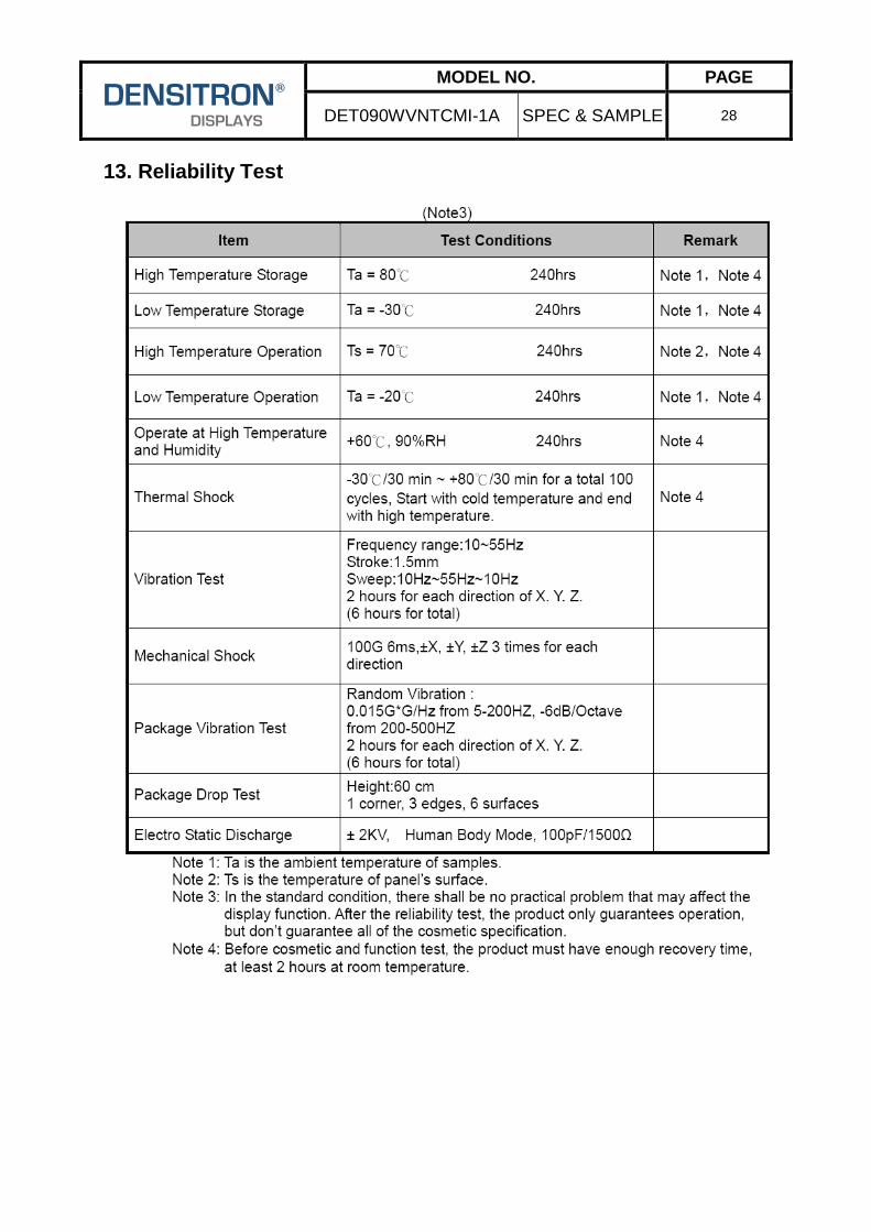
DET090WVNTCMI-1A SPEC & SAMPLE 28
DENSITRON® DISPLAYS
13. Reliability Test

MODEL NO. PAGE
DET090WVNTCMI-1A SPEC & SAMPLE 29
DENSITRON® DISPLAYS
14. Packaging
6
7
1
2
3
5
4

MODEL NO. PAGE
DET090WVNTCMI-1A SPEC & SAMPLE 30
DENSITRON® DISPLAYS
15. Precautions
15.1 Assembly and Handling Precautions
(1) Do not apply rough force such as bending or twisting to the module during
assembly.
(2) It’s recommended to assemble or to install a module into the user’s system
in clean working areas. The dust and oil may cause electrical short or worsen
the polarizer.
(3) Don’t apply pressure or impulse to the module to prevent the damage of
LCD panel and Backlight.
(4) Always follow the correct power-on sequence when the LCD module is turned
on. This can prevent the damage and latch-up of the CMOS LSI chips.
(5) Do not plug in or pull out the I/F connector while the module is in operation.
(6) Do not disassemble the module.
(7) Use a soft dry cloth without chemicals for cleaning, because the surface of
polarizer is very soft and easily scratched.
(8) Moisture can easily penetrate into LCD module and may cause the damage
during operation.
(9) High temperature or humidity may deteriorate the performance of LCD module.
Please store LCD module in the specified storage conditions.
(10) When ambient temperature is lower than 10ºC, the display quality might be
reduced. For example, the response time will become slow.
15.2 Safety Precautions
(1) If the liquid crystal material leaks from the panel, it should be kept away from
the eyes or mouth. In case of contact with hands, skin or clothes, it has to be
washed away thoroughly with soap.
(2) After the module’s end of life, it is not harmful in case of normal operation and
storage.
15.3 Terms of Warrant
(1) Acceptance inspection period
The period is within one month after the arrival of contracted commodity at the
buyer’s factory site.
(2) Applicable warrant period
The period is within twelve months since the date of shipping out under normal
using and storage conditions.

MODEL NO. PAGE
DET090WVNTCMI-1A SPEC & SAMPLE 31
DENSITRON® DISPLAYS
16.Outline Drawing
MODEL NO. PAGE
DET090WVNTCMI-1A SPEC & SAMPLE 32
DENSITRON® DISPLAYS
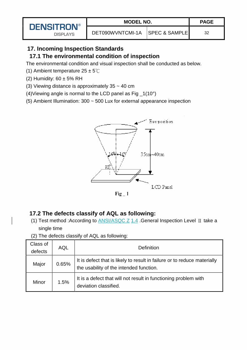
17. Incoming Inspection Standards
17.1 The environmental condition of inspection
The environmental condition and visual inspection shall be conducted as below.
(1) Ambient temperature 25 ± 5℃
(2) Humidity: 60 ± 5% RH
(3) Viewing distance is approximately 35 ~ 40 cm
(4)Viewing angle is normal to the LCD panel as Fig _1(10°)
(5) Ambient Illumination: 300 ~ 500 Lux for external appearance inspection
17.2 The defects classify of AQL as following: (1) Test method :According to ANSI/ASQC Z 1.4 .General Inspection Level Ⅱ take a
single time
(2) The defects classify of AQL as following:
Class of
defects AQL Definition
Major 0.65% It is defect that is likely to result in failure or to reduce materially
the usability of the intended function.
Minor 1.5% It is a defect that will not result in functioning problem with
deviation classified.

MODEL NO. PAGE
DET090WVNTCMI-1A SPEC & SAMPLE 33
DENSITRON® DISPLAYS
17.3 Inspection Parameters

MODEL NO. PAGE
DET090WVNTCMI-1A SPEC & SAMPLE 34
DENSITRON® DISPLAYS
Incoming Inspection Touch Panel

MODEL NO. PAGE
DET090WVNTCMI-1A SPEC & SAMPLE 35
DENSITRON® DISPLAYS
Note1. The definition of dot defect :
The dot defect was judged after repair and the size of a defective dot over 1/2 of whole
dot is regarded as one defective dot.
Note2.
W
L
Note3. D:Diameter D=(a+b)/2
Note4. Bright dot is defined through 6% transmission ND Filter as following.
Note5. ADJACENT DOT

MODEL NO. PAGE
DET090WVNTCMI-1A SPEC & SAMPLE 36
DENSITRON® DISPLAYS
Note6.
17.4 Handling of LCM
(1)Don't give external shock.
(2)Don't apply excessive force on the surface.
(3)Liquid in LCD is hazardous substance. Must not lick and swallow. when the liquid is
attach to your hand, skin, cloth etc. Wash it out thoroughly and immediately.
(4)Don't operate it above the absolute maximum rating.
(5)Don't disassemble the LCM.
B:BM
A:AA