Embed Size (px)
Citation preview
Linac 4 LL RF Hardware Architecture and Design Status
Reported by John C. Molendijk CERN-BE-RF-CS
J.C. Molendijk - Linac 4 Hardware Architecture and Design Status 12010-05-27
Gregoire Hagmann, Jose Noirjean, Donat Stellfeld, Daniel Valuch, Julien Lollierou, Anirban Krishna Bhattacharyya, Philippe Baudrenghien
CERN-BE-RF-FB
John C. Molendijk CERN-BE-RF-CS
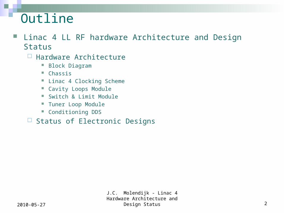
Outline Linac 4 LL RF hardware Architecture and Design Status
Hardware Architecture Block Diagram Chassis Linac 4 Clocking Scheme Cavity Loops Module Switch & Limit Module Tuner Loop Module Conditioning DDS
Status of Electronic Designs
J.C. Molendijk - Linac 4 Hardware Architecture and Design Status 22010-05-27
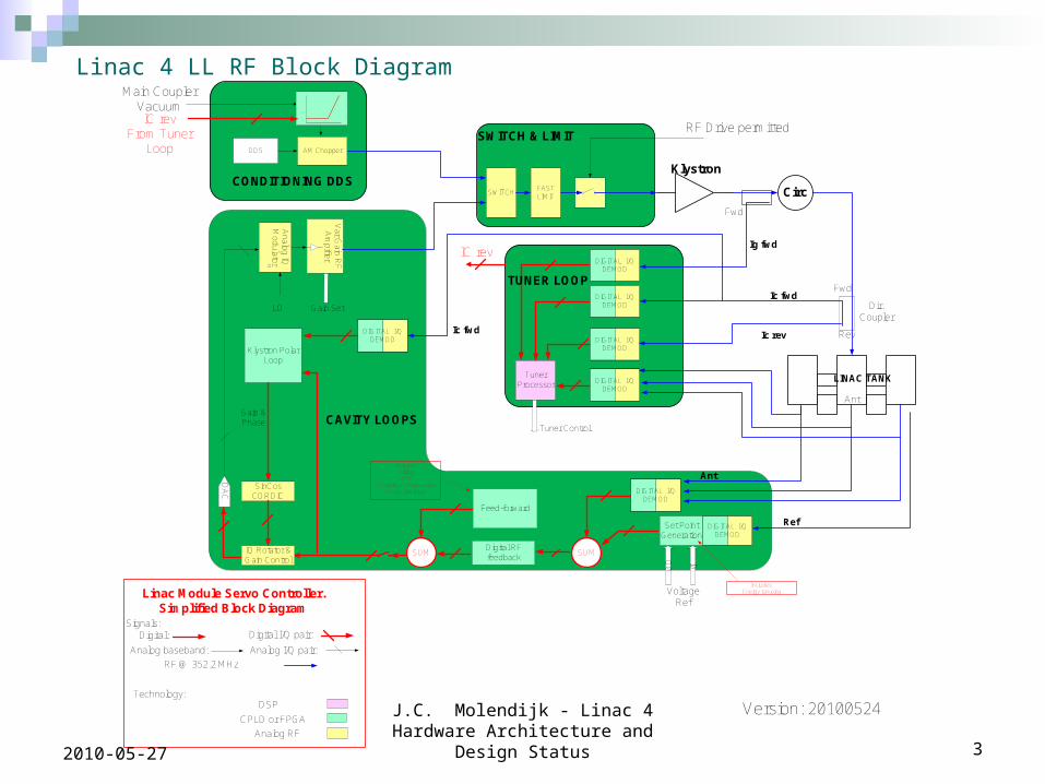
Linac Module Servo Controller. Simplified Block Diagram
Technology: DSP
CPLD or FPGA
Analog RF
Signals:Digital:
Analog baseband:
Digital I/Q pair:
Analog I/Q pair:
Tuner Processor
Dir. Coupler
Fwd
Rev
DA
C
Digital RF feedback
Ic fwd
Ic rev
TUNER LOOP
CAVITY LOOPS
Klystron
Circ
Ig fwd
Klystron Polar Loop
Feed-forward
Tuner Control
Ic fwd
CONDITIONING DDS
SWITCH & LIMIT
SWITCH
Analog IQ
M
odulator
IQ Rotator &Gain Control
LO
Var G
ain RF
A
mpifier
DDS AM Chopper
Main Coupler Vacuum
FAST LIMIT
RF Drive permitted
DIGITAL I/Q DEMOD
DIGITAL I/Q DEMOD
DIGITAL I/Q DEMOD
DIGITAL I/Q DEMOD
DIGITAL I/Q DEMOD
Fwd
Ant
RF @ 352.2 MHz
LINAC TANK
Voltage Ref
I0Q0
Set Point Generation
SUM
DIGITAL I/Q DEMOD
DIGITAL I/Q DEMOD
Ref
Ant
SUM
Version: 20100524
Includes:FillingAFF
Chopping CompensationEnergy ramping?
Includes:Energy ramping
SinCos CORDIC
Gain & Phase
IC revFrom Tuner
Loop
Gain Set
IC rev
Linac 4 LL RF Block Diagram
J.C. Molendijk - Linac 4 Hardware Architecture and Design Status 32010-05-27
Linac 4 LL RF Chassis Private backplane (Based on LHC LL RF system)
Low noise Analog power supplies. Fully buffered, Quad low-jitter differential clock distribution. Hardware Timing distribution for chopping information etc. Serial distribution of Reference RF phase. 220 mm deep slots offering sufficient real-estate for RF circuitry. Geographical VME addressing. Crate-wide JTAG enabling remote FPGA flashing through the crate
manager module.
J.C. Molendijk - Linac 4 Hardware Architecture and Design Status 42010-05-27
CLO
CK
DIS
TR
IBU
TIO
N
TU
NE
R L
OO
P
CO
ND
ITIO
NIN
G D
DS
SW
ITC
H &
PR
OT
EC
TIO
N
CA
VIT
Y L
OO
PS
CM
M
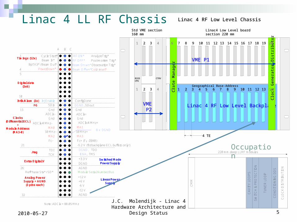
220 mm deep LLRF modules 160 mm deep
OTS
CP
U
CT
RV
Tim
ing
Linac 4 LL RF Chassis
J.C. Molendijk - Linac 4 Hardware Architecture and Design Status 52010-05-27
AGND
-12 V
-6 V
+6 V
+12 V
RefPhase Sta* / SD*
Analog Power Supply + AGND
(3 pins each)
+3.3 V Extra Digital V
Timings (12x)
Digital data(3x6)
LINAC 4 LLRF backplaneLower connector: 3 x 32 pins
version 24/05/2010
Intlk/Alarm (3x)
A B C
1
32
DGND
Linear Power Supply
Switched Mode Power Supply
Cold reset*
Observation Trig*
Post-mortem Trig*
AnalyzeTrig*
AGND
Gnd
Clocks (Differential ECL)
+Module Address
(MA3-0)
ADClk-
ADClk/4 MHz-
10 MHz-
Fc-
Gnd
Gnd
MA0
MA2
Fc+ (FIF /2048)
10 MHz+
ADClk/4 MHz+
ADClk+
8 x DGND
-5.2 V (for backplane ECL buffers only!)
Gnd
MA1
MA3
TDI
TCK
DGND, TDO
!ENA, TMS Jtag
FG SDin DGND, SDout
4
5
10
13
21
26
ConfigDone
Cycle Start*
Beam In*
See page 2
BpTA3* / Beam Out*
PowerDown*
RF ON*
RF OFF*
Beam On wn*
Beam Off wn*
Inj Enable
Module Serial Number Bus
Note: ADClk = 88.05 MHz
Linac 4 RF Low Level Chassis
Std VME section160 mm
Linac4 Low Level boardsection 220 mm
1 2 3 4 5
VME P2
1 2 3 4 6 7 8 9 10 11 12 13 14 15 16 17 18 19 205
VME P1
1 2 3 4 6 7 8 9 10 11 12 13 145
Linac 4 RF Low Level Backplane
0Geographical Base-Address
Cra
te M
an
ag
er
Clo
ck G
en
era
tor
Dis
trib
uto
r
CTRVRIO3CPU
0 14
201 4 6
1 4
4 TE
Occupation
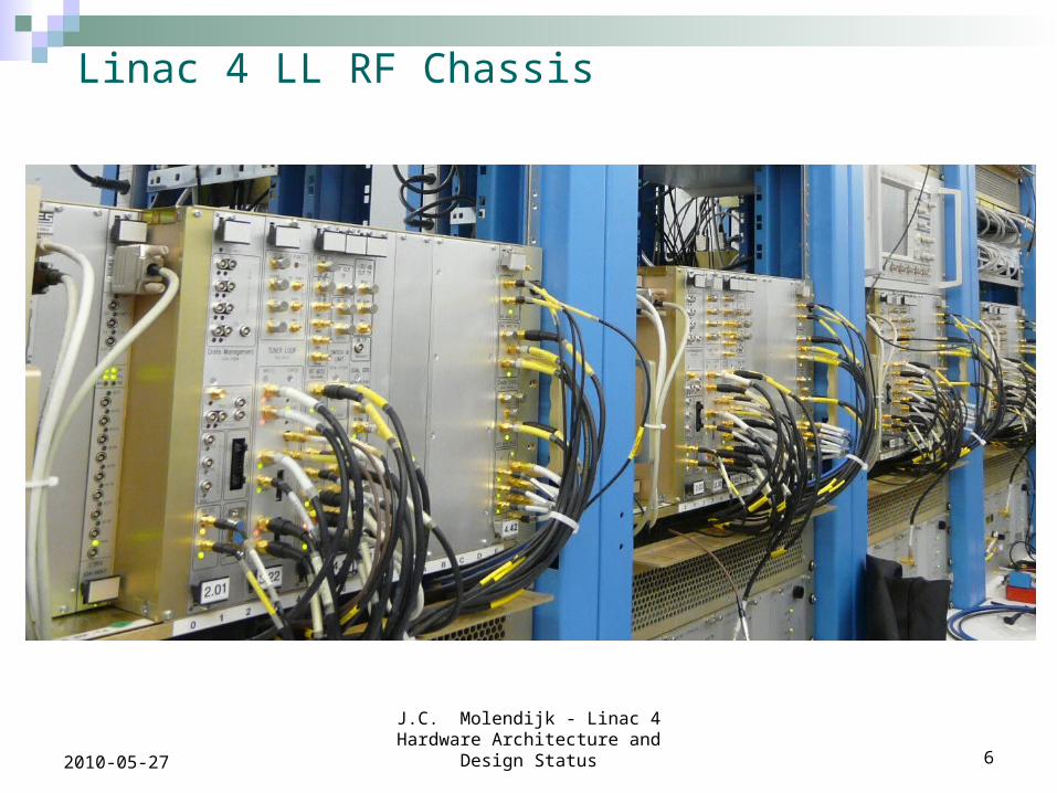
Linac 4 LL RF Chassis
J.C. Molendijk - Linac 4 Hardware Architecture and Design Status 62010-05-27
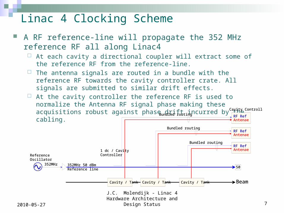
Linac 4 Clocking Scheme
A RF reference-line will propagate the 352 MHz reference RF all along Linac4 At each cavity a directional coupler will extract some of the reference RF from the
reference-line. The antenna signals are routed in a bundle with the reference RF towards the
cavity controller crate. All signals are submitted to similar drift effects. At the cavity controller the reference RF is used to normalize the Antenna RF
signal phase making these acquisitions robust against phase drift incurred by the cabling.
J.C. Molendijk - Linac 4 Hardware Architecture and Design Status 72010-05-27
Clock Generation
Designer
Date Version
PageTitle
John C. Molendijk BE/RF/cs
2010/03/26
EDA-0xxxx
352MHz 352MHz 50 dBmReference line
50
1 dc / CavityController
RF RefAntenae
RF RefAntenae
Cavity ControllersBundled routing
Bundled routing
Cavity / Tank Cavity / Tank
ReferenceOscillator
Cavity / Tank
RF RefAntenae
Bundled routing
Beam
Linac 4 Clocking Scheme
Clocks Required for RF LL Reference RF. Local Oscillator (LO) for the mixers (Receivers and Modulators). ADC clock (4 * fIF). ADC clock /2 and ADC clock /4 for IQ demodulation. 10 MHz reference clock.
Critical Clocks Reference RF, LO and ADC clock must have very low phase noise (jitter) to
minimize demodulation errors and to maintain the effective number of bits (ENOB) in the Digital RF Receivers.
J.C. Molendijk - Linac 4 Hardware Architecture and Design Status 82010-05-27
I1 Q1 -I2 -Q2
Inverted Signal
I3 Q3 -I4Signal
Offs
TunerCtrl applies 2 stage CIC with R=16 => Average over I/Q 16 (even) samples => Offset Cancelled.
0Intended Signal
Moving Average over 1 cyclefor PM & Observation MemoryFull 40MSPS rate & Offset compensation!
(Ii + Offs) - (-Ii+1 + Offs)
2I'i =
(Qi + Offs) - (-Qi+1 + Offs)
2Q'i =
12.5 ns
20050615 J.C.Molendijk CERN AB/RF
TADClk
Clock Generation
Designer
Date Version
PageTitle
John C. Molendijk BE/RF/cs
2010/03/26
EDA-0xxxx
RF inLPF
ADClk =4 * fIF
LO
IF
0 1
+1 -1 ADClk/4
01
ADClk/2
I
Q
Digital IQ Demodulator
Analog Domain Digital Domain
Typical Digital RF ReceiverIQ Sampling & ADC Offset Compensation
Linac 4 Clocking Scheme LHC case
The beam synchronous RF is generated in SR4 (surface building) and then optically transported to the UX45 (cavern) faraday cages.
All RF synchronous clocks are there derived from the SR4 reference by one central clock Generator per beam.
A distribution system supplies the reference RF and all generated clocks (380, 80, 40 and 20 MHz) to all 8 cavity controllers crates per beam.
Linac 4 Reference RF is generated from a high quality Oscillator which is then amplified
(~100W) to drive the Linac 4 RF reference line. All RF synchronous clocks are derived and distributed within each cavity
controller. Big savings in distribution and improved clock signal quality. The Locally generated and distributed LO does not have to be phase drift
stabilized since both the down and up convertors use the same (see p13). The cavity controller’s Clock Generator Distributors receive and demodulate the
Reference RF. The measured phase is distributed serially over the backplane to allow all modules to normalize their acquisitions. No need for individual ref. RF receivers per module.
Only the absolute 10 MHz reference is distributed individually.
J.C. Molendijk - Linac 4 Hardware Architecture and Design Status 92010-05-27
Linac 4 Clocking Scheme Clock Generator Distributor per Cavity Controller
J.C. Molendijk - Linac 4 Hardware Architecture and Design Status 102010-05-27
Clock Generation
Designer
Date Version
PageTitle
John C. Molendijk BE/RF/cs
2010/03/26
EDA-0xxxx 1/4Overview
3.0source: G:\Departments\AB\Groups\RF\Machines\Linac4\LowLevel\Diagrams\ClockGenDistriv3.dsf
352MHz
99
9
9 10MHz to Cavity Controllers
Ref RF IN
RF OUT
RF OUT Splitter
Front Panel
f/KADClk OUT
ADClk OUT
ADClk / 4 OUT
LL RF Backplane
SplitterFc OUT10 kHz
Fc OUT
10MHz IN 10MHz OUT
LO OUT
LO OUTto Fdbk
LO OUTto TunerLO OUTto SwAp
50
50
50
Nim Distribution
f/4
DividersLinac4:SPL: N=32, M=31, K=8
N=16, M=15, K=4
Splitter
Frequencies:
IF = 22.0125 MHzLinac4 LO = 330.1875 MHz SPL LO = 682.3875 MHzADClk = 88.05 MHz
Linac4 RF = 352.2 MHz SPL RF = 704.4 MHz
For LegacyCompatibility.
Via FrevBackplane
Count = 3once per 2048
14.3 ns
Via MHz40Backplane
Via MHz10Backplane
10MHz
352MHz 50 dBmReference line
50
Att
50
50
PhaseDetector
Ref. Phase Serial OUT
LO OUTVCOf/N
f/M22MHzLO
1 dc / CavityController
LO
ClockDistri Principle
SN65EPT20? (single)SN65EPT22 (double)
0 dBm
0 to 1 dBm4 way
0 dBm
0 to 1 dBm
100-800MHz
100-800MHz
Clock Generation
Designer
Date Version
PageTitle
John C. Molendijk BE/RF/cs
2010/03/26
EDA-0xxxx Clock Distributor 3/4
Ref Line
VectoringCORDIC
RF
LO MHz
I
Q
IQ Demod
AD
Clk
/ 2
AD
Clk
/ 4
LPF50
LPF32k
I
AD
Clk
Q
2 kS/sADClk MS/s
Zn
Diag ro Register
Ref Phase
FPGA
VRef Level
ADClkDiv(1,0)
FcDiv(1,0) Div = 3by 2048
Via FrevBackplane
Count = 3once per 2048
TADClk
ro Registers
3.0
Via 40 MHzBackplane
Routing delay <= Fc routing delay.
Div(1) Via 20 MHzBackplane
22 MHz
ADClk
Ref PhaseSerializer
Start
SD
Start
SD27a
27b
Via SpareBackplane bus
-1
FRev
D Q
Clr
TTL to LVPECL
ResyncEna D Q D Q
Q
RF
SyncB
D Q
Clr
'1'
DQ
ClrClr
PDC
RF-TP
FRevTP
SyncIn SyncHS
AD9512 ADClk MHzresyncDivide by K
Prog
Q
88 MHzsplit 3 ECL+ LVCMOS
ADClk
Linac 4 Clocking Scheme Phase Discriminator
J.C. Molendijk - Linac 4 Hardware Architecture and Design Status 112010-05-27

Linac 4 Clocking Scheme
J.C. Molendijk - Linac 4 Hardware Architecture and Design Status 122010-05-27
New Low noise LO PLL and distribution
Designer J. Lollierou
N =15
R =16
LO L4 Jitter = 270 fs, Band integrated [10Hz-10MHz]
LO LHC Jitter=264 fs
f/R
f/N
Phase
Detector
LPF VCO
f1
f2
Clk1
Clk1B
Clk2Clk2B
ADF4106
Using std VCO
LO L4 Jitter= 120 fs
Using Coaxial resonator based VCO
Retained solution
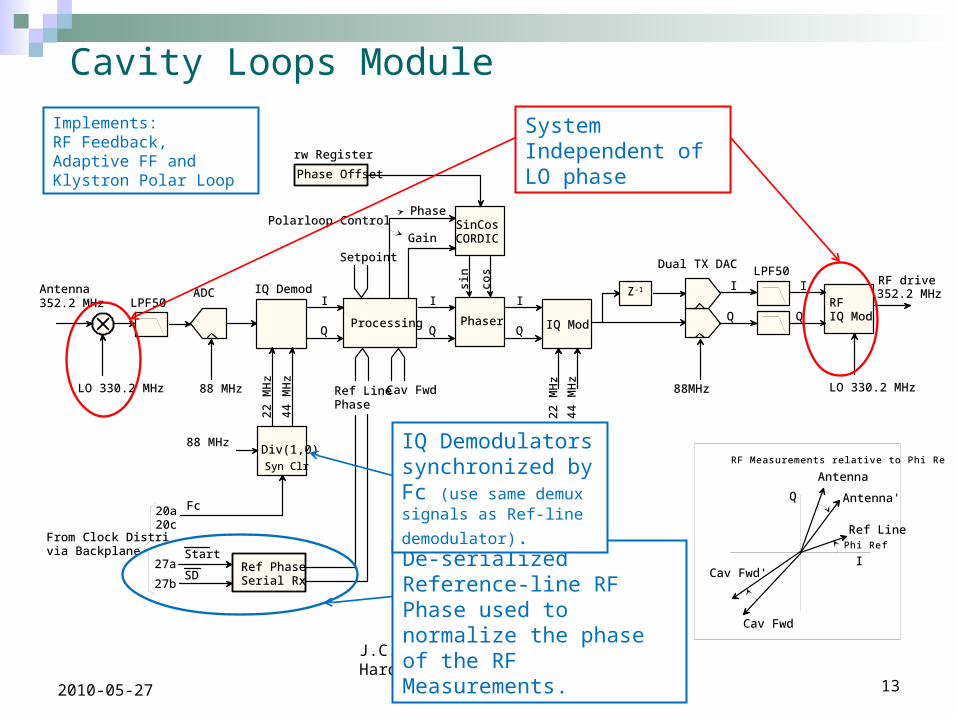
Cavity Loops Module
J.C. Molendijk - Linac 4 Hardware Architecture and Design Status 132010-05-27
RF Feedback Linac4
Designer
Date Version
PageTitle
John C. Molendijk BE/RF/cs
2009/05/05
EDA-0xxxx
352.2 MHz
LO 330.2 MHz 88 MHz
I
Q
IQ Demod
Processing
Setpoint
Ref LinePhase
Cav Fwd
Antenna
Phaser
SinCosCORDIC
sin
cos
Phase
Gain
I
Q
I
Q IQ Mod
Z-1 I
Q
Dual TX DAC
RFIQ Mod
LO 330.2 MHz
352.2 MHzRF drive
88MHz
44 M
Hz
22 M
Hz
I
QLPF50
Antenna
I
Q
Ref LinePhi Ref
Antenna'
RF Measurements relative to Phi Ref.
Cav Fwd
Cav Fwd'
LPF50
Principle
1.0
1/1
44 M
Hz
22 M
Hz
Div(1,0)88 MHz
Fc
Syn Clr
Ref PhaseSerial Rx
Start
SD27a
27b
From Clock Distrivia Backplane
20a20c
Phase Offset
rw Register
ADC
Polarloop Control
De-serialized Reference-line RF Phase used to normalize the phase of the RF Measurements.
System Independent of LO phase
IQ Demodulators synchronized by Fc (use same demux signals
as Ref-line demodulator).
Implements:RF Feedback,Adaptive FF andKlystron Polar Loop
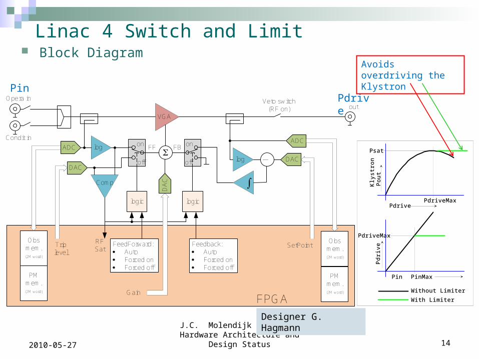
Linac 4 Switch and Limit Block Diagram
J.C. Molendijk - Linac 4 Hardware Architecture and Design Status 142010-05-27
Comp
VGA
log
Obs mem.(2M word)
logic
on
off
FeedForward:· Auto· Forced on· Forced off
DACDAC
ADC
―log
logic
∫
ADC
Feedback:· Auto· Forced on· Forced off
DA
C
Trip level
Gain
SetPoint
on
off
Veto switch(RF on) out
Opera in
Condit in
RF Sat
FPGA
FF FB
PM mem.(2M word)
PM mem.(2M word)
Obs mem.(2M word)
Record length (Only PM, zero Obs):· Full rate 44MSPS (I/Q pair), Fs=88MHz· PMtime = 91ms (2 channels), 4M words = 2M I/Q pairs => 48ms· PMtime = 182ms (1 channel), 8M words = 4M I/Q pairs => 95 ms
Switch and Limit
Designer G. Hagmann
Pdrive
Without Limiter
With Limiter
Pd
rive
Pin
PdriveMax
PinMax
Po
ut
Psat
PdriveMax
Kly
stro
n
PinPdrive
Avoids overdriving the Klystron

Linac 4 Tuner Loop Front-end Simplified Block Diagram
J.C. Molendijk - Linac 4 Hardware Architecture and Design Status 152010-05-27
Designer J. Noirjean
Coupler ADC
PwrDet
LPF
Digital IF signal to IQ
demodulators
8 x channels
RF input IF
RF level
IF differential
FPGA
LO
Chebyshev 5th order, fc = 35 MHz
Tuner Front-end
LPF
Chebyshev 3rd order, fc = 385 Mhz
ADC driver
Tuner Control
Samtec controlled impedance connection
J.N., 25.05.2010
Tuner Loop
ADC Clk
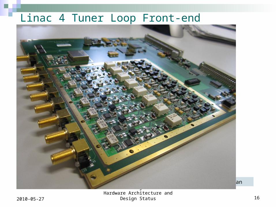
Linac 4 Tuner Loop Front-end
J.C. Molendijk - Linac 4 Hardware Architecture and Design Status 162010-05-27
Designer J. Noirjean
Linac 4 Tuner Loop Module Simplified Block Diagram
J.C. Molendijk - Linac 4 Hardware Architecture and Design Status 172010-05-27
Designer J. Noirjean
Tuner Linac4
Designer
Date Version
PageTitleJohn C. Molendijk BE/RF/csJose Noirjean BE/RF/fb
2009/05/06
EDA-0xxxx
352.2 MHz
LO 330.2 MHz
AD
Clk
MH
z
I
Q
IQ DemodAntenna
-Ref Phase
AD
Clk
/2
AD
Clk
/ 4
LPF50
Antenna
I
Q
Ref LinePhi Ref
Antenna'
RF Measurements relative to Phi Ref.
Cav Fwd
Cav Fwd'
SinCosCORDIC
CrossProd
Phaser
sin(
Z0'
)
cos(
z0')
I
Q
Phase Set
SinCosCORDIC
Z0
Z0'
sin(Z0)
cos(Z0)
sin(Z0')
cos(Z0')
CIC16_2
352.2 MHz
LO 330.2 MHz
I
Q
IQ DemodIcFwdLPF50
Phaser
sin(
Z0)
cos(
z0)
I
Q
CIC16_2
+
To ExternalMemory
E_IcFwd
PowerProd
Vcav 2A
DC
lk M
Hz
Tuner FE Tuner Cntrl
88 MS/s 88 / 16 MS/s
Phase Add
I Q
I
Q
To ExternalMemory
I
Q
Signal Principle
1.0
1/1
Ref PhaseSerial Rx
Start
SD27a
27b
Div(1,0)ADClk MHz
Fc
Syn Clr
20a20c
AD
Clk
/ 2
AD
Clk
/ 4
DSP Tuning Control
E_IcFwd = Vcav X IcFwd
Optimal Vcav Phase
Common for all Linac4 structures: DSP orSoftware customized,L. Arnaudon
VME register
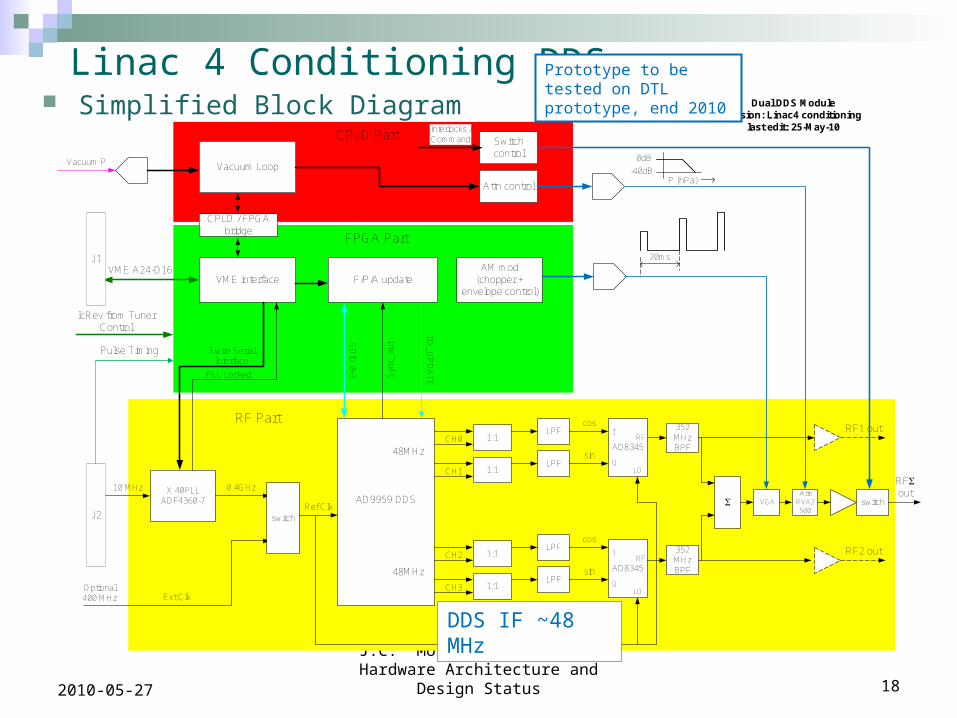
Linac 4 Conditioning DDS Simplified Block Diagram
J.C. Molendijk - Linac 4 Hardware Architecture and Design Status 182010-05-27
J2
10 MHz
Dual DDS Module version: Linac4 conditioning
last edit: 25-May-10
0.4GHz
Ext Clk
switch
48MHz
AD9959 DDS
48MHz
352 MHz BPF
RF1 out
Ref Clk
RF Part
X 40PLLADF4360-7
F/P/A update
SD
IO 0-3 S
ync_
out
Attn control
VME interface
Vacuum P Vacuum Loop
FPGA Part
I/O_U
PD
AT
E
Attn RVA2500
CH0 1:1LPF
cos
CH1 1:1LPF
sin
CH3 1:1LPF
sin
CH2 1:1LPF
cos
AD8345
I
QLO
RF
switch
RF out
352 MHz BPF
RF2 out
VGA
AD8345
I
QLO
RF
Switch control
AM mod (chopper +
envelope control)
CPLD Part
20ms
0dB
-40dBP (hPa)
J1VME A24-D16
CPLD / FPGA bridge
Optional 400 MHz
Interlocks / Command
PLL Locked
IcRev from Tuner Control
Pulse Timing 3 wire Serial Interface
DDS IF ~48 MHz
Prototype to be tested on DTL prototype, end 2010
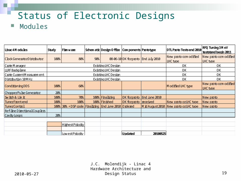
Status of Electronic Designs Modules
J.C. Molendijk - Linac 4 Hardware Architecture and Design Status 192010-05-27
Linac 4 Modules Study Firmware Schematic Design Office Components Prototype DTL Proto Tests end 2010RFQ Tuning 3 MeV teststand begin 2011
Clock Generator Distributor 100% 80% 90% 08-06-10 OK for proto End July 2010New proto or modified LHC type
New proto or modified LHC type
Crate Manager OK OKLLRF Backplane OK OKCrate Current Measurement OK OKDistribution 10 MHz OK OK
Conditioning DDS 100% 60% Modified LHC typeNew proto or modified LHC type
Chopper Pulse Generator 20%Switch & Limit 100% 70% 100% Finalizing OK for proto End June 2010 New protoTuner Front-end 100% 100% 100% Finished OK for proto received New proto or LHC type New protoTuner Control 100% 30% + DSP code Finalizing End June 2010 Ordered Mid August 2010 New proto or LHC type New protoRef-line Directional CouplersCavity Loops 20%
Highest Priority
Lowest Priority Updated 20100525
Existing LHC Design
Existing LHC DesignExisting LHC DesignExisting LHC Design

Thank you for your attention.
J.C. Molendijk - Linac 4 Hardware Architecture and Design Status 202010-05-27