Embed Size (px)
Citation preview

UG0821User Guide
Chip Planner Libero SoC v12.0

MicrosOne ECA 92WithinOutsidSales:Fax: +Email:www.m
©2018 subsidiarights reMicroseMicroseand serrespect
ty of f the ave ny
not to emi ly
P this is
io of
d d's on
emi Headquartersnterprise, Aliso Viejo,656 USA the USA: +1 (800) 713-4113 e the USA: +1 (949) 380-6100 +1 (949) 380-61361 (949) 215-4996 [email protected]
Microsemi, a wholly owned ry of Microchip Technology Inc. All served. Microsemi and the mi logo are registered trademarks of mi Corporation. All other trademarks vice marks are the property of their ive owners.
Microsemi makes no warranty, representation, or guarantee regarding the information contained herein or the suitabiliits products and services for any particular purpose, nor does Microsemi assume any liability whatsoever arising out oapplication or use of any product or circuit. The products sold hereunder and any other products sold by Microsemi hbeen subject to limited testing and should not be used in conjunction with mission-critical equipment or applications. Aperformance specifications are believed to be reliable but are not verified, and Buyer must conduct and complete all performance and other testing of the products, alone and together with, or installed in, any end-products. Buyer shallrely on any data and performance specifications or parameters provided by Microsemi. It is the Buyer’s responsibilityindependently determine suitability of any products and to test and verify the same. The information provided by Microshereunder is provided “as is, where is” and with all faults, and the entire risk associated with such information is entirewith the Buyer. Microsemi does not grant, explicitly or implicitly, to any party any patent rights, licenses, or any other Irights, whether with regard to such information itself or anything described by such information. Information provided indocument is proprietary to Microsemi, and Microsemi reserves the right to make any changes to the information in thdocument or to any products and services at any time without notice.
About MicrosemiMicrosemi, a wholly owned subsidiary of Microchip Technology Inc. (Nasdaq: MCHP), offers a comprehensive portfolsemiconductor and system solutions for aerospace & defense, communications, data center and industrial markets. Products include high-performance and radiation-hardened analog mixed-signal integrated circuits, FPGAs, SoCs anASICs; power management products; timing and synchronization devices and precise time solutions, setting the worlstandard for time; voice processing devices; RF solutions; discrete components; enterprise storage and communicatisolutions, security technologies and scalable anti-tamper products; Ethernet solutions; Power-over-Ethernet ICs and midspans; as well as custom design capabilities and services. Learn more at www.microsemi.com.
50200821-2.0.0/12.18

Revision 2.0 3
Contents
Introduction . . . . . . . . . . . . . . . . . . . . . . . . . . . . . . . . . . . . . . . . . . . . . . . . . . . . . . . . . . . . . . . . . . . . . . 4
1 Chip Planner Views . . . . . . . . . . . . . . . . . . . . . . . . . . . . . . . . . . . . . . . . . . . . . . . . . . . . . . . . . . . . . . . . 6
2 Display Options Window . . . . . . . . . . . . . . . . . . . . . . . . . . . . . . . . . . . . . . . . . . . . . . . . . . . . . . . . . . . 31
3 Floorplanner View Window. . . . . . . . . . . . . . . . . . . . . . . . . . . . . . . . . . . . . . . . . . . . . . . . . . . . . . . . . . 35
4 Other Chip Planner Windows . . . . . . . . . . . . . . . . . . . . . . . . . . . . . . . . . . . . . . . . . . . . . . . . . . . . . . . . 40
5 Floorplanning Using Chip Planner . . . . . . . . . . . . . . . . . . . . . . . . . . . . . . . . . . . . . . . . . . . . . . . . . . . . 41
6 Netlist Views. . . . . . . . . . . . . . . . . . . . . . . . . . . . . . . . . . . . . . . . . . . . . . . . . . . . . . . . . . . . . . . . . . . . . 49
7 Cross-Probing from SmartTime to Chip View/Netlist View. . . . . . . . . . . . . . . . . . . . . . . . . . . . . . . . . . 51
B Limitations . . . . . . . . . . . . . . . . . . . . . . . . . . . . . . . . . . . . . . . . . . . . . . . . . . . . . . . . . . . . . . . . . . . . . . 58

Introduction
Chip Planner is a Graphical Interface Tool that provides a Chip View and a Netlist View. The Chip View allows you to create regions, edit regions, and make logic assignments to regions. It is a floorplanning tool used to improve the timing performance and routability of your design by providing maximum control over your design object placement. The Netlist Viewer provides a schematic view of the design that allows you to examine the routing of the nets and reveal any routing congestions.You can also cross-probe from SmartTime into Chip Planner to browse your design and look into timing problems.
Use Chip Planner to:• View macro assignments made during layout.• Assign, unassign, or move macros.• Lock macro assignments.• View net connections using a ratsnest view.• View architectural boundaries.• View and edit silicon features, such as I/O banks.• Create Regions and assign macros or nets to regions (floorplanning).• View logic placement and net connections to investigate timing problems together with
SmartTime’s Cross-Probing feature.• View the hierarchical netlist after Synthesis and the flattened netlist after Compile• Create logical cones for debugging and detailed analysis.
You must run Synthesis and Compile Netlist on your design before invoking Chip Planner. If you do not, Libero runs Synthesis and Compile Netlist before opening Chip Planner. You can invoke Chip Planner for floorplanning after running Place and Route to improve routability and remove congestion.
When floorplanning, you analyze your design to see if certain logic can be grouped within regions. Placement regions are especially useful for hierarchical designs with plenty of local connectivity within a block. If your timing analysis indicates several paths with negative slack, try grouping the logic included in these paths into their own regions. This forces the placement of logic within the path closer together and may improve timing performance of the design.
Supported Families and PlatformsChip Planner supports SmartFusion2, IGLOO2, RTG4, and PolarFire devices and runs on Windows and Linux systems.Note: Depending on the device selected, some UI elements such as icons, options, and dialog boxes may
vary slightly in appearance and/or content. Basic Chip Planner functionality remains the same, regardless of the device chosen.
Invoking Chip Planner Invoke Chip Planner from the Constraint Manager (Design Flow window > Manage Constraints > Open Manage Constraints View > Constraint Manager > Floor Planner > Edit with Chip Planner).Note: You must complete the Synthesis or Compile step before invoking Chip Planner from the Constraint
Manager. If you do not, a pop-up message appears telling you to run these steps first.
Revision 2.0 4

PDC Files When Chip Planner opens, only the PDC file(s) associated with Place and Route are loaded into Chip Planner for reading. PDC files in your project not associated with Place and Route are ignored.When you make an I/O or floorplanning change in Chip Planner, commit, and save, the change is saved to a *.pdc file that you have set as target in the Constraint Manager. If no PDC constraint file is set as target, the change is written to a new user.pdc file. When the change is related to floorplanning, the user.pdc file is displayed in the Floor Planner tab. When the change is related to I/Os, the user.pdc file is displayed in the I/O Attributes tab.The I/O PDC files are located in the <proj>\constraints\io folder.The Floorplanning PDC files are located in the <proj>\constraints\fp folder.
Chip Planner Splash ScreenThe Chip Planner splash screen appears when the Chip Planner tool is invoked.
Chip Planner and PDC Commands/FilesChip Planner is an interactive tool for floorplanning. The floorplanning changes you make in Chip Planner are saved as PDC (Physical Design Constraints) commands in PDC file(s). Interactive floorplanning actions in Chip Planner have corresponding PDC commands which can be made part of a constraint file for Place and Route. For details about Libero SoC PDC commands, refer to the PDC Commands User Guide.Chip Planner and other tools have access to and write to the same PDC file(s). When more than one of these tools are opened, making and saving changes (from any one tool) is not allowed. This is to prevent the user from inadvertently overwriting the constraints in the PDC file(s). A message pops up to alert you to the modification conflict and tells you what tool or tools are open and need to be closed.To fix the modification conflict:
1. Close the tool or tools and leave only one tool open.2. Make and save the changes in the tool.
Figure 1 • Chip Planner Splash Screen
Revision 2.0 5
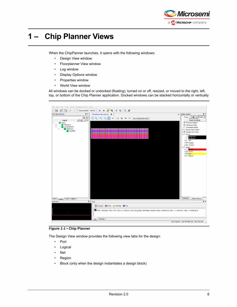
1 – Chip Planner Views
When the ChipPanner launches, it opens with the following windows:• Design View window• Floorplanner View window• Log window• Display Options window• Properties window• World View window
All windows can be docked or undocked (floating), turned on or off, resized, or moved to the right, left, top, or bottom of the Chip Planner application. Docked windows can be stacked horizontally or vertically
The Design View window provides the following view tabs for the design:• Port • Logical• Net • Region • Block (only when the design instantiates a design block)
Figure 1-1 • Chip Planner
Revision 2.0 6

Table 1-1 lists the icons in the toolbar. Hover the mouse on the icon shown in the Floorplanner View to see the tooltip.
Clone and Clear OptionsThe Clone and Clear options appear when you right-click on the main object browser/design view window. Table 1-2 describes these options.
Table 1-1 • Chip Planner Toolbar Icons
Icon Name Function
Commit Commit and Save will:• Run Chip Planner DRC before saving the
changes. • Write/Update the PDC files.
Undo Reverse your last action.
Redo Reverse the action of your last Undo Command.
Highlight Highlight a net, macro or a port.
Unhighlight All Unhighlight all highlighted selections (macro, net or port).
Table 1-2 • Chip Planner Clone and Clear Options
Icon Name Function
Clone new filter Clone a Find window for a specific view (Logical/Port/Net/Region/Block) depending on the view you are in when you click this icon or CTRL + F. Multiple Find windows may be cloned, each with a different set of filtering criteria, to give you multiple filtered views of design elements.
Delete all filter browsersDelete all port filter browsersDelete all net filter browsersDelete all region filter browsersDelete all block filter browsers
Deletes all cloned Find windowsDeletes all cloned port filter windowsDeletes all cloned net filter windowsDeletes all cloned region filter windowsDeletes all cloned block filter windows
Rename Rename the cloned window to a name other than the default name
Revision 2.0 7
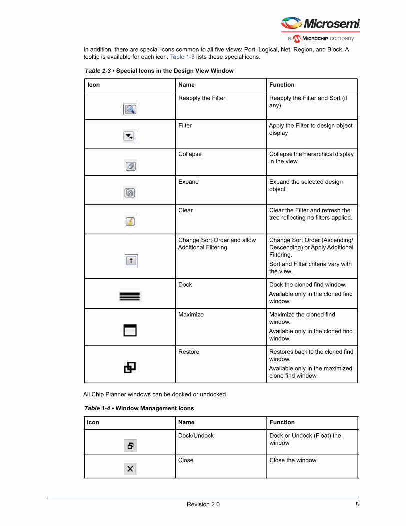
In addition, there are special icons common to all five views: Port, Logical, Net, Region, and Block. A tooltip is available for each icon. Table 1-3 lists these special icons.
All Chip Planner windows can be docked or undocked.
Table 1-3 • Special Icons in the Design View Window
Icon Name Function
Reapply the Filter Reapply the Filter and Sort (if any)
Filter Apply the Filter to design object display
Collapse Collapse the hierarchical display in the view.
Expand Expand the selected design object
Clear Clear the Filter and refresh the tree reflecting no filters applied.
Change Sort Order and allow Additional Filtering
Change Sort Order (Ascending/Descending) or Apply Additional Filtering.Sort and Filter criteria vary with the view.
Dock Dock the cloned find window.Available only in the cloned find window.
Maximize Maximize the cloned find window. Available only in the cloned find window.
Restore Restores back to the cloned find window.Available only in the maximized clone find window.
Table 1-4 • Window Management Icons
Icon Name Function
Dock/Undock Dock or Undock (Float) the window
Close Close the window
Revision 2.0 8

Chip Planner provides the following special keys and hot keys.
Table 1-5 • Special Keys/Hot Keys
Hot Keys/Special Keys Function
CTRL + F Find/Search function. Creates a cloned Find Window.
CTRL + Z Undo the last action/command.
CTRL + S Save all changes.
CTRL + Y Redo last action/command.
Home Scroll to the first selected item in the view.
End Scroll to the last selected item in the view.
Tab Scroll to the next selected item in the view.
Shift + Tab Scroll to the previous selected item.
CTRL + Q Exit Chip Planner
CTRL + ++ Zoom In
CTRL + -- Zoom Out
CTRL + 0 Zoom to Fit
CTRL + H Lock All Macros
SHIFT + CTRL + H Unlock All Macros
Hold SHIFT + Left_Mouse Click Select multiple elements in Design View WindowsWhen you select two items, those items and all item between them are selected.
Hold CTRL + Left Mouse click Select multiple elements in Design View Windows
ESC Unselect all selected items. Remove any pop-up windows
<Right Arrow key> Select Element at next level of hierarchy in design flow window
<Left Arrow key> Select element at previous level of hierarchy in design flow window.
<Down Arrow key> Select next element at the same level of hierarchy in design flow window
<Up Arrow key> Select previous element at the same level of hierarchy in the design flow window.
Revision 2.0 9

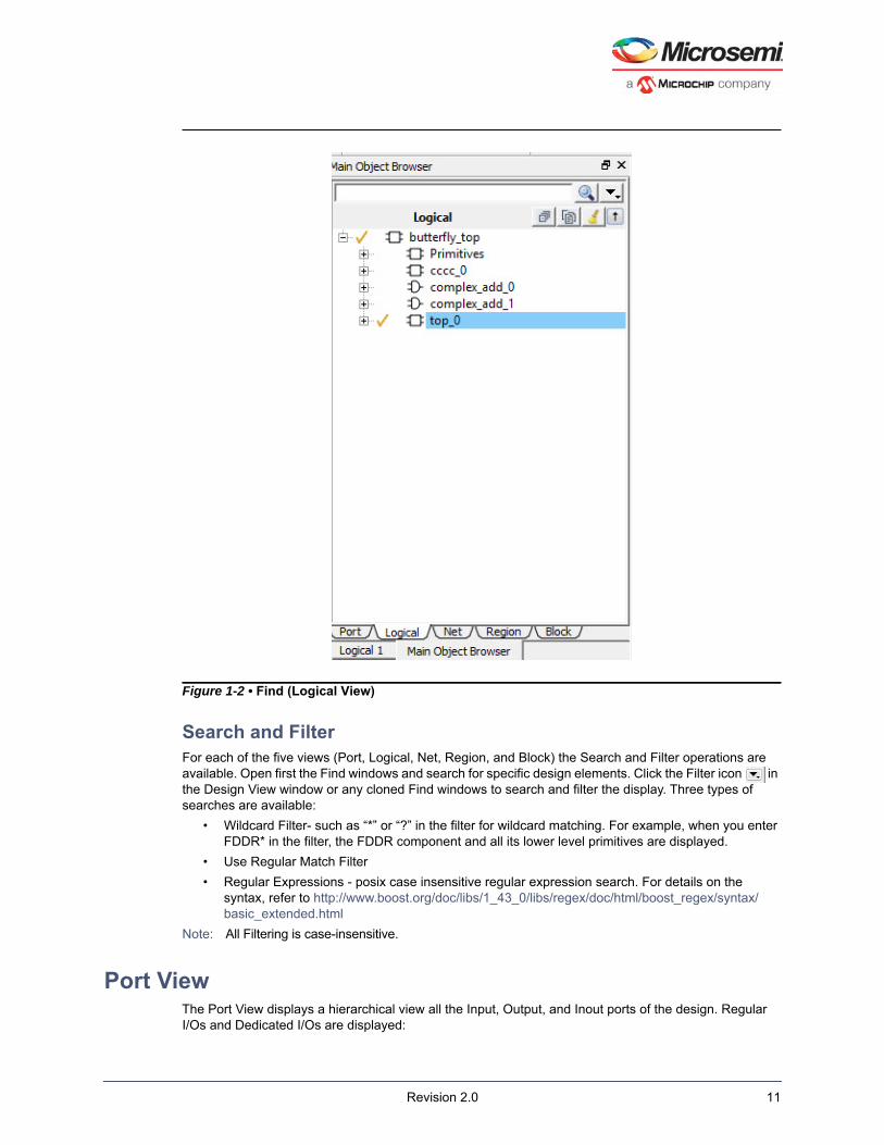
Design View Window and View TabsWhen Chip Planner opens, it presents a Design View Window with five view tabs:
• Port• Logical• Net• Region• Block - only if user blocks (*.cxz files) exist in the design
Each of the view tabs displays a design view. A selection of a design element in one view is reflected in other views. For example, when you click and select a bus port in the Port view, the Logical view shows the OUTBUF/INBUF primitives (for the bus) selected and the Net view shows the net (connected to the INBUF/OUTBUF of the port) selected. Similarly, when a user region is selected in the Region view, the selection is reflected in the Floorplanner View as well.The Design View window can be docked and undocked.
Find WindowChip Planner provides a Find window for each of the five design views to search for design elements. You can also use the CTRL- F Hot Key. Multiple Find windows can be created for the same design view (Port/Logical/Net/Region/Block).When the Find window opens, it is associated with a specific design view. Only design elements specific to the particular view are displayed. The view name (Port/Logical/Net/Region/Block) is displayed across the top of the window. You can create multiple cloned Find windows for each view. Cloned Find windows are floating when they are opened and can be resized, moved, docked or undocked (floating).When the Find window is invoked in the Logical view, for example, the find window opens with the name Find (Logical) across the top of the window and the name Find # (Logical) across the top of the window when there are multiple cloned Find windows for the same View. By default, each cloned Find window is named sequentially as Find 1 (<view_name>), Find 2 (<view_name>), Find 3 (<view_name>) and so on. The cloned Find Windows can be renamed to a name different from the default.A cloned Find Window has the same features and functionality as the main view window. In addition, a cloned Find Window has this extra icon:
• Rename Tree - Renames the cloned Find Window to a name different from the default name.You may find multiple find windows useful in floorplanning. For example, If your design has both a RAM and a MACC block and you want to filter and select both and display them in the Floorplanner View, you need two Find windows for the logical view, one with the filter based on Macro type > RAM and the other with the filter based on Macro type > MACC.
Revision 2.0 10
Search and Filter For each of the five views (Port, Logical, Net, Region, and Block) the Search and Filter operations are available. Open first the Find windows and search for specific design elements. Click the Filter icon in the Design View window or any cloned Find windows to search and filter the display. Three types of searches are available:
• Wildcard Filter- such as “*” or “?” in the filter for wildcard matching. For example, when you enter FDDR* in the filter, the FDDR component and all its lower level primitives are displayed.
• Use Regular Match Filter• Regular Expressions - posix case insensitive regular expression search. For details on the
syntax, refer to http://www.boost.org/doc/libs/1_43_0/libs/regex/doc/html/boost_regex/syntax/basic_extended.html
Note: All Filtering is case-insensitive.
Port ViewThe Port View displays a hierarchical view all the Input, Output, and Inout ports of the design. Regular I/Os and Dedicated I/Os are displayed:
Figure 1-2 • Find (Logical View)
Revision 2.0 11

• Regular I/O ports - Input/Output/Inout ports that can be changed or reassigned by the user. These are shown under the I/O Ports tree.
• Dedicated I/Os - Special-purpose I/Os that cannot be changed or reassigned by the user. These are shown under the Dedicated Ports tree.
Figure 1-3 • Port View
Port BusesScalar members of a bus port are grouped under the bus. All bus ports can be collapsed or expanded.
Figure 1-4 • Bus Port DATA_OUT and its scalar members
Revision 2.0 12

Port PropertiesTo see the properties of the port, click to select the port. The properties of the port you selected is displayed in the "Properties Window". The selected port is also highlighted in the Floorplanner View and the World View.
User Actions in Port ViewIn the Port View, you can:
• Place ports to locations - Select a port and drag and drop the port into the Floorplanner View at a valid resource location to assign the element to that location. All valid port locations are highlighted when you drag the selected element into the Floorplanner View.
• Unplace ports from locations - Right-click the port and choose Unplace From Location to unassign a port.
• Lock Port to location - Right-click the port and choose Lock Placement to lock selected port to the assigned location. This option is enabled only when the port is already placed in a location.
• Unlock Port from location - Right-click the port and choose Unlock Placement to unassign the port. This option is enabled only when the port is already locked to a location.
• Region Assign - Right-click a port and choose Region Assign. The Select Region dialog opens, and shows the regions available to assign that element. This dialog opens even if there are no User regions that the selected item can be assigned to. See the following example.
• Unassign Port from Region - Right-click the port and choose Unassign Macro to Region to un-assign a port macro from a region. This option is enabled only if the port is already assigned to a region.
• Unassign All - Right-click the port and choose Unassign All to unassign all the ports that are assigned to regions.
• Unassign Selected Ports - Right-click the port and choose Unassign Selected Ports to unassign all the selected ports that are assigned to regions.
• Check DRC rules of selected interface - For a selected interface, DRC rules can be verified by selecting this option. A message in the log window informs the user whether the DRC rule check is successful or not.
SortingClick the sort icon to sort the Ports in ascending or descending order, the type, and the state of the ports.
Revision 2.0 13

Port FilteringEither the traditional match filter or Regular Expression match filter is available. Enter a port name in the Filter text box to filter Ports. Enable the Use RegEx checkbox to use Regular Expression match filtering.
Filter According to Port TypesThe Port Filter list varies with the family and die. See “Family-specific Macros/Nets/Ports” on page 64 for details.
Filter According to Port StatesPort States filtering includes:
• Placeable - All I/O that can be placed by the user.• Unplaceable - All I/O that cannot be placed by the user, example: dedicated I/O.• Assigned to location- All I/O that can be assigned to a location.• Not assigned to location - All I/O that cannot be assigned to a location.• Assigned to region - All I/O that can be assigned to a region.• Not assigned to region - All I/O that cannot be assigned to a region.• Locked - All I/O that are locked.• Unlocked - All I/O that are not locked.
Table 1-6 lists the icons and the functions of the ports in the Port View.
Table 1-6 • Ports and Icons
Icon Name Function
Input Port Represents an Input Port.
Output Port Represents an Output port.
Bidirectional Port Represents a Bi-Directional port.
White Background Represents a port that is not placed.
Green Background Represents a port that is placed.
Blue Tick Mark Represents an I/O that has been assigned to a region.
Lock Icon Represent an I/O that is fixed/ locked to a location.
Revision 2.0 14

Logical ViewThe logical view is accessible from the Logical tab of the Design View window.It displays a hierarchical view of all the logic inside the chip. The displayed Logic levels are:
• Component - Displays the logic at the component level. This represents the hierarchy in the design.
• Primitives - Displays the lowest level of the hierarchy (hard macro level).You can expand the hierarchy tree to see the lower level logic.
Logic Element PropertiesClick the component/primitive to find out the properties of the logic element you have selected. The properties of the component/primitive are displayed in the "Properties Window". The selected design element is also highlighted in the Floorplanner View and in the World View.
User Action in Logical ViewSelect a design element to:
• Assign elements to locations - Right-click a design element and choose Place to Location to assign the element to that location. All valid resource locations are highlighted in the Floorplanner View when you drag the selected element into the Floorplanner View. Only a single element can be assigned at a time.
• Unassign element from location - Right-click a design element and choose Unplace from Location. You can select multiple design elements/components and unassign them.
• Lock element to location - Right-click a design element and choose Lock Placement to lock the selected element to an assigned location. This option is enabled only when the element is already placed in a location. You can select multiple design elements/components and lock them.
• Unlock element from location - Right-click a design element and choose Unlock Placement to unlock or unfix a design element that is already locked to a location. This option is enabled when the element is already locked to a location. You can select multiple design elements/components and unlock them.
• Region assign - Right-click a design element and choose Region Assign. A new Select Region dialog opens providing you different regions available to assign that element. This dialog pops up even if there is no User regions, the selected item can be assigned to
• You can also drag and drop the selected elements directly into a region in the Floorplanner View. If the selected elements are not compatible or over-booked for the desired region, the selection is not assigned to the region and invalid elements are shown in red in the Properties window.
• Unassign element from region - Right-click a design element and choose Unassign Macro from Region to unassign a design element/macro from a region. This option is enabled only if the element is already assigned to a region. You can select multiple design elements/components and unassign them from a region.
• Unassign all - Right-click the port and choose Unassign All to unassign all the elements that are assigned to regions.
• Unassign selected ports - Right-click the port and choose Unassign Selected Ports to unassign all the selected elements that are assigned to regions.
FilteringEnter a macro name in the Filter text box to filter the design elements. From the pull-down menu of the Sort icon, choose either the traditional match filtering, wildcard filtering, or Regular Expression match filtering.
Revision 2.0 15

Sorting Click the Sort Icon to sort in ascending or descending order, the type (Filter by Macro Type), and state (Filter by State) of the logic element.
Figure 1-5 • Macro Filter
FilteringEnter a macro name in the Filter text box to filter the design elements. From the pull-down menu of the Sort icon, choose either traditional match filtering, wildcard filtering, or Regular Expression match filtering.
According to Macro TypesAvailable Macro types are family/die-dependent. See Appendix A, "Cross-Probing from SmartTime to Chip View/Netlist View"for the list of Macro filters specific to the family/technology of your project.
According to Macro StateThe Logical View displays the filter results based on the state of the Logical elements:
• Placeable - All Macro that can placed by the user. This option is mutually exclusive with the Unplaceable option.
• Unplaceable - All Macro that cannot be placed by the user. This option is mutually exclusive with the Placeable option.
• Assigned to Location - All Macro that can be assigned to a location. This option is mutually exclusive with the Not assigned to Location option.
• Not assigned to Location - All Macro that cannot be assigned to a location. This option is mutually exclusive with the Assigned to Location option.
• Assigned to Region - All Macro that can be assigned to a region. This option is mutually exclusive with the Not assigned to Region option.
• Not assigned to Region - All Macro that cannot be assigned to a region. This option is mutually exclusive with the Assigned to Region option.
• Locked - All Macro that are locked. This option is mutually exclusive with the Unlocked option.
Revision 2.0 16
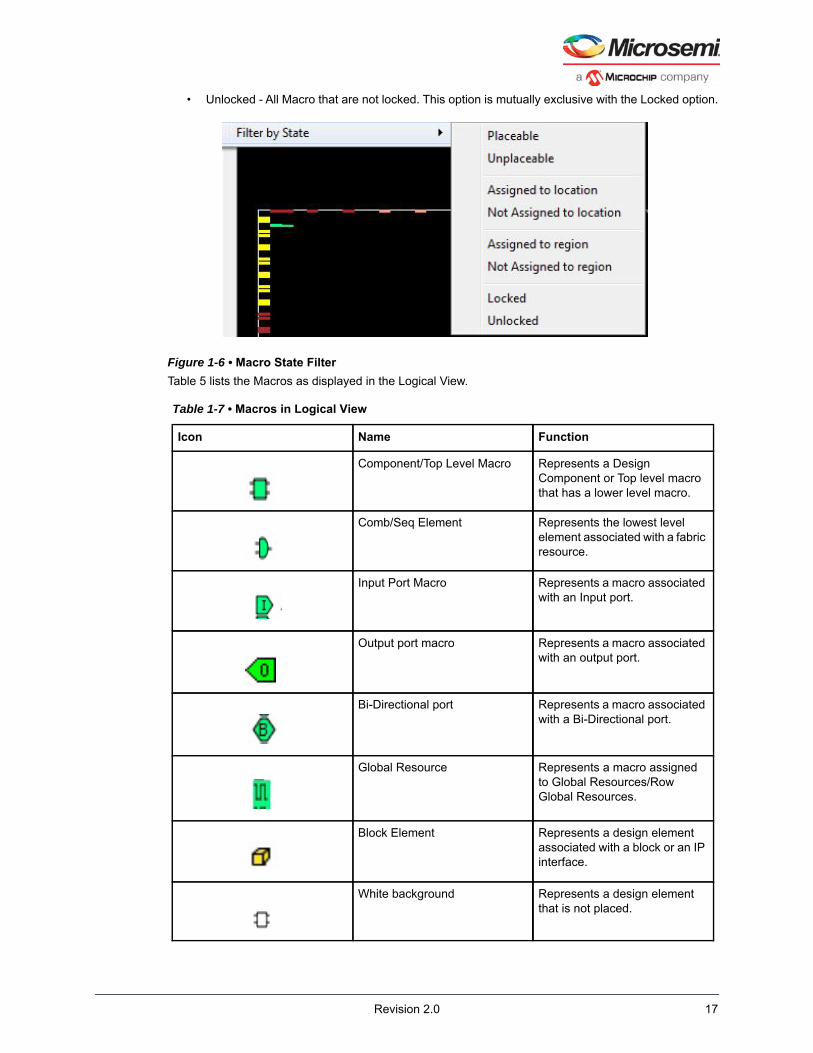
• Unlocked - All Macro that are not locked. This option is mutually exclusive with the Locked option.
Figure 1-6 • Macro State FilterTable 5 lists the Macros as displayed in the Logical View.
Table 1-7 • Macros in Logical View
Icon Name Function
Component/Top Level Macro Represents a Design Component or Top level macro that has a lower level macro.
Comb/Seq Element Represents the lowest level element associated with a fabric resource.
Input Port Macro Represents a macro associated with an Input port.
Output port macro Represents a macro associated with an output port.
Bi-Directional port Represents a macro associated with a Bi-Directional port.
Global Resource Represents a macro assigned to Global Resources/Row Global Resources.
Block Element Represents a design element associated with a block or an IP interface.
White background Represents a design element that is not placed.
Revision 2.0 17

Net ViewThe Net View displays a flattened net view of the design and all the nets associated with the design. Shown with each net are the pins connected to the net.
Figure 1-7 • Net View
Green background Represents a design element that is placed.
Blue tick mark Represents a design element that has been assigned to a region.
Lock Icon Represents a design element that is fixed/locked to a location.
Table 1-7 • Macros in Logical View (continued)
Icon Name Function
Revision 2.0 18

Net PropertiesClick to select the net and the net properties are displayed in the "Properties Window". The selected net is also highlighted in the Floorplanner View and the World View.
User Actions in Net ViewFrom the Net view, you can:
• Change Net Color - Right-click a net and choose Net Color to change the net color. This opens a color palette from which you can assign the desired color to the selected net.
• Region Assign - Right-click a design element and choose Region Assign. The Select Region dialog opens, and shows the regions available to assign that element. This dialog opens even if there are no User regions that the selected item can be assigned to. See the following example.
• Check the Assign with Driver check box to assign all the net macros including driver macros to a region. This option is enabled if there is a valid Region created over the required resources. You can select multiple nets and assign them to a region.
• UUnassign All - Right-click the port and choose Unassign All to unassign all the nets that are assigned to regions.
• Unassign Selected Nets - Right-click the port and choose Unassign Selected Nets to unassign all the selected nets that are assigned to regions.
Sorting Sort the nets in ascending or descending order.
FilteringEnter a net name in the Filter text box to filter net names. From the pull-down menu of the Sort icon, choose either traditional match filtering, wildcard filtering, or Regular Expression match filtering. You can also filter with criteria specific to nets, such as fanout values, net types, and routing status (routed or unrouted).
Filter Criteria based on fanout value• Max Fanout - Enter a value to display nets with a maximum fanout value.• Min Fanout - Enter a value to display nets with a minimum fanout value.
Note: Max Fanout and Min Fanout are logical ANDed together. If the Max Fanout has a value of 10 and the Min Fanout has a value of 2, the Net view displays only nets which meet both conditions. In this case, only nets with a fanout range of 2 to 10 are displayed.
Revision 2.0 19

Filter Criteria based on net typeThe net type and the filter list is family/die-specific. See Appendix A, "Cross-Probing from SmartTime to Chip View/Netlist View" for the list of net filters specific to the family/technology of your project.
Filter Criteria based on routing status• Routed - Displays all routed nets• Unrouted - Displays all unrouted nets
Figure 1-8 • Net Filter OptionsTable 1-8 lists the icons specific to the net view.
Table 1-8 • List of Net Icons
Icon Name Function
Regular/Hardwired Net Represents a regular or hardwired net.
Global Net Represents a net that is routed through Chip Global/Row global resources.
Driven Macros Represents a list of macros that are driven by this net.
Driver macros Represents a macro that is driving this net.
Blue tick mark Represents a net that has been assigned to a region.
Revision 2.0 20

Global NetsA global net is a net that uses Global routing resources for routing a signal from source to destination logic clusters. These include Chip Globals Resources/Global Buffers (GB), Row global resources/row global buffers (RGB), and Half-Chip Globals (HGB for RTG4). Clocks, Async Reset, and nets with high fanout are typically routed through these global routing resources. Global signals (G[n:0]) reach the logic clusters through row global signals (RG[7:0]) generated by an associated row global buffer (RGB). RGB are inferred by the layout tool and depending on the placement of the design elements, it distributes the fanout of the global nets across multiple RGBs. The Net View shows this break-up for such global nets.An example of a Global Net routed through GB[0] with a fanout of 2968 is shown in the Properties window below.
Figure 1-9 • Global Net Information in Properties WindowThe Floorplanner View of the Global Net is shown in Figure 1-10.
Figure 1-10 • Chip Planner View of Global Net Routed Through GB[0]
Region ViewThe Region View displays the regions you have created and all Components, Macros, and Nets assigned to the region. When you create a region, by default the region is named UserRegion1, UserRegion2, and so on. When you make a selection in the Region View, the properties of the Region you select are displayed in the "Properties Window". When you select an item in the hierarchical tree display, all sub-items are selected.
Revision 2.0 21

Figure 1-11 • Region View
User Regions and Region TypesThree types of regions are available for creation:
• "Inclusive Region"• "Exclusive Region"• "Empty Region"
User Actions on Regions in Floorplanner ViewYou can select a region in the Floorplanner View to:
• Delete - Deletes a selected region. • Clone - Clones a selected region.• Rename - Renames a selected region.• Merge - Merges two or more regions. This option is enabled if there are more than two regions
selected.• Assign macros inside Region - Assigns macros that are part of a region area assigned to the
selected region.• Unplace From location - Unassigns all design elements that are part of a selected region from
their placed locations. • Lock Placement - Locks all macros that are part of a selected region.• Unlock Placement - Unlocks all macros that are part of a selected region. • Unassign All - Unassigns all the elements from a region.• Unassign Selected Ports - Unassigns all the selected ports from a region.• Unassign Selected Nets - Unassigns all the selected nets from a region.• Unassign Selected Components - Unassigns all the selected components from a region.
Revision 2.0 22

Region PropertiesClick the region in the Region View and the properties of the region you have selected are displayed in the "Properties Window". The selected region is also highlighted in the Floorplanner View and the World View.
Region FilteringEnter a region name in the Filter text box. From the pull-down menu of the Sort icon, choose traditional match filtering, wildcard filtering, or Regular Expression match filtering.
Region SortingIn addition to ascending or descending order display, a filter is available for the Region View to display user regions based on region types:
• Inclusive - shows all inclusive regions• Exclusive - shows all exclusive regions• Empty - shows all empty regions
Figure 1-12 • Region FilterThe table below lists Region View icons.
Table 1-9 • Region View Icons
Icon Name Function
Inclusive Represents an inclusive region.
Exclusive Region Represents an exclusive region.
Empty Region Represents an Empty region.
Nets Represents a net associated with a region.
Revision 2.0 23

Block ViewThe block view displays the low-level design blocks (*.cxz files) you have imported into the Libero SoC project. This tab appears only if and when design blocks exist in the project. These low-level design blocks may have completed the place-and-route step and met the timing and power requirements of the design block. For details, refer to the Block Flow User Guide (Help > Reference Manuals).
Component / Top Level Macro Represents a Design Component or Top level macro that have lower level macros.
Comb / Seq Element Represents the lowest level element associated with a fabric resource.
Output port macro Represents a macro associated with an output port.
Input Port Macro Represents a macro associated with an Input port.
Green background Represents a design element that is placed.
Blue tick mark Represents a design element that has been assigned to a region.
Lock Icon Represents a design element that is fixed/locked to a location.
Table 1-9 • Region View Icons (continued)
Icon Name Function
Revision 2.0 24

The Block View displays all the design blocks in the project and displays the following design elements for each design block:
• Macros• Nets• Ports
Block PropertiesClick to select the block in the Block View and the properties of the block are displayed in the "Properties Window". The selected block is also highlighted in the Floorplanner View and the World View.
Block FilteringEnter a block name in the Filter text box to filter blocks. From the pull-down menu of the Sort icon, choose traditional regular match filtering, wildcard filtering or regular expression match filtering.You can sort the blocks in ascending or descending order.
Properties WindowThe Properties window displays the properties of the design elements. What is displayed in the Properties window is dependent on what is selected in the design view.
Properties of Logical View ElementsThe Properties window displays the properties of a component or macro when it is selected in the Logical View. Properties displayed may include the following, depending on the type of design elements:
Figure 1-13 • Block View Example
Revision 2.0 25

• Macro/Component Name - Full Macro or component name based on selection in logical view.• Cell Type - Resource type based on design element selection.• Placed (Location) - X-Y coordinates where device element is placed.• Resource Usage Table - A table showing resources based on component and macro selection.• Region Attached Table - A table showing region to which selected macro/component is assigned.• User region (if any) it is attached to.• Nets Table - A table showing pins and nets which is associated with the selected macro along
with fanout value.• Locked/Unlocked (Placement) - The selected port is locked or unlocked.• Port - Port name to which the I/O macro is assigned (only shown for I/O port macros).• I/O Technology Standard - I/O Technology which is associated with the selected I/O macro (only
shown for I/O port macros).• I/O Bank- I/O bank to which the selected I/O macro is assigned (only shown for I/O port macros).• Pin (Package Pin) - Pin to which the macro is assigned (only shown for I/O port macros).
Note: Not all properties in the list are displayed. The list of displayed properties varies with the type of design element selected in the Logical View.
Figure 1-14 • Example of Properties Window (Logical View)
Properties of Port View ElementsWhen a design element (I/O Bus or Scalar I/O) is selected in the Port View, the Properties window displays the properties of a bus (for I/O bus) or a macro (for scalar I/Os) For an I/O bus, the Properties window displays:
• Resource Usage Table - Shows all resources associated with the selection.• Ports Table: Displays a table with I/O Bank, I/O Technology Standard, Package Pin, and Port
Names of each individual member of the bus.For scalar I/O ports, the Properties window displays the Macro information:
Revision 2.0 26

• Port Name - Full Name of the selected port.• Macro - Name of the macro associated with the selected port.• Port Type of selected I/O.• Placed (Location) - X-Y coordinates where device element is placed.• Locked/Unlocked (Placement) - Selected port is locked or unlocked.• Pin (Package Pin name) - Pin name to which selected port is assigned.• I/O Technology Standard - I/O standard that is associated with the port.• I/O Bank - I/O Bank associated with the selected port.• Resource Usage table.• Nets Table - A table showing pins and nets associated with the selected port along with fanout
value.
Figure 1-15 • Example of Properties Window (Ports View)
Properties of NetsFor nets selected in the Net view, the Properties window displays the following:
• Net Name - Full name of the selected net.• Driver Name - Macro that is driving the selected net.• Fanout - Fanout value of the selected net.• Type of Net: Regular/Hardwired/Global for the selected net. • State: Routed or Unrouted net
Revision 2.0 27

Figure 1-16 • Example of Properties Window (Net)
Properties of RegionRegion properties are displayed in the Properties window when a user region is selected in the Floorplanner View or in the Region View.The properties window for a region displays the following:
• Region Name - By default, the regions are named UserRegion1, UserRegion2, and so on when first created. You can change the region name by editing the Region name text box in the Properties window.
• Type of Region (Inclusive/Exclusive/Empty)• Routing Requirements
– Constrain routing - Instructs the Place and Route tool to apply routing restrictions (in addition to Placement restrictions) to the user regions. Refer to Figure 1-17 • Example of Properties Window (Region) for details.
• Region Extents - Displays the X-Y coordinates of the origin (lower left corner) and the endpoint (upper right corner) and the width and height of the region.
• Resources in the Region - Displays the logic resources in the region, including used (Assigned) resources and total available resources (Capacity) and a percentage of used resources (Assigned) relative to the total resources (Capacity). A percentage greater than 100 indicates resource overbooking, which is not allowed. The overbooked resource is highlighted in red.
Revision 2.0 28

Properties of BlocksWhen a block is selected in the Block View, the Properties window displays:
• Block Name - Name of the selected block.• Module Name - Name of the block module.• Macro Count - Total number of macros in the block.• Net Count - Total number of nets in the block.• Locked Count - Total number of locked macros.
In addition, it specifies whether all the macros are placed and/or routed.
Figure 1-17 • Example of Properties Window (Region)
Revision 2.0 29

Figure 1-18 • Properties of Block
Revision 2.0 30

2 – Display Options Window
The Display Options Window allows you to customize the layout and the color settings for design elements on the Floorplanner View to meet your personal preferences.There are three default layers and colors settings group that are provided with Chip Planner:
• System• Pin_Planner• Grey_Scale
By default, Chip Planner launches with “System” layers and colors settings group for the Device (Silicon feature) and the Design Elements. These are the System Default Settings..
Figure 2-1 • Default Color Setting for Device (Silicon Hardware) - Settings shown are for MPF300TS die (PolarFire)
The device color setting is a hierarchical view. You may expand each group to see the lower level items and see the default color setting for each. The device cell types, IO banks are die-dependent and reflects the available hardware components for the selected die.Similarly the color setting for the Design Elements are displayed in a hierarchical view. Expand the group to see the default color setting for each lower level design element.
Changing Color SettingsTo change the color setting for a device or design element from the default setting:
Revision 2.0 31

1. Right-click the color for the element.2. In the Set Color Dialog Box, move the Cross across the color spectrum to the color you prefer.3. Click OK.
Figure 2-2 • Set Color Dialog Box to Change Color
Displaying an Instance in the Floorplanner View using the Display Options WindowYou can use the checkbox provided against each menu item to select the elements you want to see in the Floorplanner View. Some of the options in Display Options window cannot be unchecked, as these options are fixed for any design. Such options have checkboxes grayed-out and are always enabled. However, you can still change the colors settings of these options Design Option in Display Options windows can be grouped according to Macro Type and State of Macro. The display of design elements in the Floorplanner View depends on both conditions met: the Macro Type and the State of macro. For example, if you want to see 4LUT elements of your design, you need to select both Movable & Placed Macro and 4LUT options.The table below lists the icons specific to the Display Options window.
Table 2-1 • Display Options Icons
Icon Name Function
Rename Settings Rename user created layers and colors settings from the default name to a name you specify
Remove Settings Remove the user defined Layers and colors settings.
Clone Settings Create a clone of current Layers and Colors Settings
Revision 2.0 32

Creating Personal Settings You can create your display settings according to your preferences.
1. Create a clone from one of the selected settings (Grey Scale, Pin Planner, System) using Clone Setting icon in the Display Options window.
Figure 2-3 • Clone Settings in Display Options Window2. Accept the default name “Group #” for the settings name or rename it from the Display Options
window.3. Change color settings and/or select items to be displayed from the Display Options window.
The customized settings can be created and preserved on your system and will always be available in the drop-down group list in the Display Options window. The customized settings are available to you across different projects on the same machine.
Removing Custom Setting GroupTo delete the custom setting group, select the custom setting group and click Remove Setting icon in Display Options window.Note: The System setting is the default group and it cannot be removed. Only user-set custom settings
can be removed.
Reset to System DefaultClick Reset <group_name> to Default to reset the group’s settings to the system default settings.
Chip Display OptionsThe following options are available in the Display Options window. They control the display in the Floorplanner View:
Fill Device Cells When this box is checked, the entire Floorplanner View is filled with all device modules at all view levels. Use this mode to see the display of all device resources on the chip. When this mode is not enabled (the default), only the devices used by the design are displayed. Device cells which are shown are dependent on the Display Options settings for Device cells.
Use Cluster ModeWhen this box is checked, the clusters (rather than the modules and macros inside the clusters) of the chip are displayed. This mode is useful when the Floorplanner View is zoomed out far enough to make the modules and macros too small to be visible. This mode significantly improves runtime performance, especially when displaying large device.The cluster will be displayed as used in the Floorplanner View if any module inside it is used. When this mode is not enabled (the default), the Floorplanner View displays down to the macro and module level. This mode may incur runtime penalty, particularly on large devices.
Revision 2.0 33

Consolidate Globals When this box is checked, the Row Globals (RGB) are hidden from the Floorplanner View. Row globals (RGB) do not exist in the user netlist. They are buffers inserted by Libero SoC after layout. When this option is turned on, the Row Globals are removed from the display and the Chip Globals are shown as directly driving the macros and cells. This view makes it easier to determine the load of the Chip Globals. To do so, there is no need to track the load from the Chip Globals to the Row Globals and then to the macros and cells.
Design Elements in Display Options WindowThe design elements displayed in the Display Options window are family and die-dependent.
Revision 2.0 34

3 – Floorplanner View Window
The Floorplanner View window displays all design elements in one window. The selections you make in the views are reflected in the Floorplanner View. The color scheme used in the canvas is dependent on the Layers and Colors you have selected in the Display Options window
Operation ModesThe Floorplanner View has two modes of operation:
• Macro Manipulation ModeUse this mode to work with macros, such as assigning macros to location or unassigning placed macros from locations. You can also view properties of selected macros in the Floorplanner View from the properties window. You can select multiple macros from the Floorplanner View by pressing the <CTRL> key and selecting required macros in the Floorplanner View.
• Region Manipulation Mode Use this mode to work on regions such as resizing, renaming, or deleting regions, or assigning and unassigning macros or nets to regions.
Click the Macro Manipulation Mode or Region Manipulation Mode button to switch modes.
Figure 3-1 • Floorplanner View
Revision 2.0 35

Floorplanner View IconsThe icons available across the top of the Floorplanner View window allows you to zoom in, zoom out, assign I/O banks, runs DRC checks, create regions for placement.
Table 3-1 lists the functions of the each icon.
Figure 3-2 • Floorplanner View Icons Across the Top of the Window
Revision 2.0 36
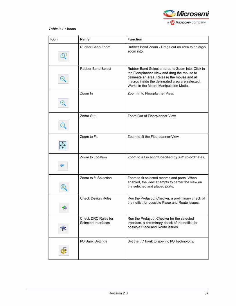
Table 3-1 • Icons
Icon Name Function
Rubber Band Zoom Rubber Band Zoom - Drags out an area to enlarge/zoom into.
Rubber Band Select Rubber Band Select an area to Zoom into. Click in the Floorplanner View and drag the mouse to delineate an area. Release the mouse and all macros inside the delineated area are selected. Works in the Macro Manipulation Mode.
Zoom In Zoom In to Floorplanner View.
Zoom Out Zoom Out of Floorplanner View.
Zoom to Fit Zoom to fit the Floorplanner View.
Zoom to Location Zoom to a Location Specified by X-Y co-ordinates.
Zoom to fit Selection Zoom to fit selected macros and ports. When enabled, the view attempts to center the view on the selected and placed ports.
Check Design Rules Run the Prelayout Checker, a preliminary check of the netlist for possible Place and Route issues.
Check DRC Rules for Selected Interfaces
Run the Prelayout Checker for the selected interface, a preliminary check of the netlist for possible Place and Route issues.
I/O Bank Settings Set the I/O bank to specific I/O Technology.
Revision 2.0 37

Netlist Viewer in Floorplanner View WindowIn addition to the chip view, the Floorplanner View window displays the netlist views. See “Netlist Views” on page 49 for details.
Auto Assign I/O Bank Run the Auto I/O Bank and Globals Assigner. Assigns a voltage to every I/O Bank that does not have a voltage assigned to it and if required, a VREF pin.
Create Empty Create an empty user region.
Create Inclusive Create an inclusive user region.
Create Exclusive Create an Exclusive user region.
Delete Region Delete user-created region you have selected.
Use the Macro Manipulation Mode and Region Manipulation Mode buttons
Click the Macro Manipulation Mode and Region Manipulation Mode buttons to switch modes.
Zoom Floorplanner View To Fit
Zoom to fit the Floorplanner View
Expand Floorplanner View To Minimum Zoom
Expands the floorplanner view to make devices visible
View Full Screen Toggle button to view full screen and restore back
Icon Name Function
Revision 2.0 38

The Floorplanner View and the Netlist View each features a different set of icons specific to that view. There is also a Floorplanner View/Netlist Viewer menu which toggles between Floorplanner View and Netlist View based on the view that is active at the time.See the following figures.
Figure 3-3 • Floorplanner Menu and Icons
Figure 3-4 • Netlist Viewer Menu and Icons
Revision 2.0 39

Revision 2.0 40
4 – Other Chip Planner Windows
World View WindowThe World View shows a red rectangle which reflects what is visible in the Floorplanner View in the context of the Chip. Changing what is visible in the canvas also changes the red rectangle. Changing the size or position of the red rectangle changes what is seen in the Floorplanner View.
Figure 4-1 • World View Window
Log WindowThe Log window displays all messages generated by Chip Planner. You can filter the messages according to the type of message: Error, Warning, and Info. If you have made and saved changes in Chip Planner, the Log Window displays the name and location of the PDC file(s) which have been edited/updated to reflect the changes.
Figure 4-2 • Log Window

5 – Floorplanning Using Chip Planner
Floorplanning includes creating regions and making logic assignments to those regions. It is an optional methodology to improve the performance and routability of your design. The objective in floorplanning is to assign logic to specific regions on the chip to enhance performance and routability. When floorplanning, you analyze your design to see if certain logic can be grouped within regions. Placement regions are especially useful for hierarchical designs with plenty of local connectivity within a block. If your timing analysis indicates several paths with negative slack, try grouping the logic included in these paths into their own regions. This forces the placement of logic within the path closer together and may improve timing performance of the design.Use floorplanning to create Design Separation Regions for security-critical designs. For Microsemi’s Design Separation Methodology, all logic should be contained in a logic placement region with dedicated place and route resources. Refer to Microsemi Design Separation Methodology for details.Use Chip Planner before and after running layout to help you floorplan. You can:
• Create Regions• Move, resize, merge, or delete regions• Assign logic to region• Assign nets to regions
Types of Regions Three region types can be created for floorplanning purposes:
• Inclusive region• Exclusive region• Empty region
Inclusive RegionIn an inclusive region, the Place-and-Route tool places unassigned logic within its boundary. It can contain macros, both assigned and unassigned to region. Routing resources within an inclusive region are also not restricted. Logic already placed there before region creation is not unplaced from the region.
Use the create Inclusive Region icon to create an Inclusive region.When a region rectangle is created, you can assign logic macros / net macros / port macros to it from the design view window.
Revision 2.0 41

You can also draw a region rectangle over placed macros and assign these macros to the region using the Assign macros inside region option by selecting the region rectangle in the Floorplanner View.
Figure 5-1 • Inclusive Region Example
Exclusive RegionIn an exclusive region, the Place-and-Route tool does not place unassigned logic within its boundary. It can contain only macros already assigned to the region before the region is created. However, routing resources within an exclusive region are not restricted.
Use the Create Exclusive Region icon to create an exclusive region.When a region rectangle is created, you can assign logic macros / net macros / port macros to it from the design view window. If an exclusive region rectangle is created over placed macros, the locked macros already inside the exclusive region will not be unplaced. They are automatically assigned to the region. If the macro is placed but not locked, the macros will be unplaced from the locations and will not be assigned to the exclusive region.
Figure 5-2 • Exclusive Region Example
Revision 2.0 42
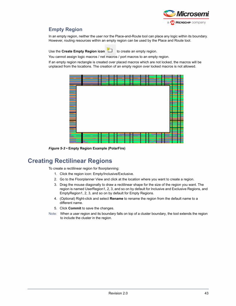
Empty RegionIn an empty region, neither the user nor the Place-and-Route tool can place any logic within its boundary. However, routing resources within an empty region can be used by the Place and Route tool.
Use the Create Empty Region icon to create an empty region.You cannot assign logic macros / net macros / port macros to an empty region.If an empty region rectangle is created over placed macros which are not locked, the macros will be unplaced from the locations. The creation of an empty region over locked macros is not allowed.
Figure 5-3 • Empty Region Example (PolarFire)
Creating Rectilinear RegionsTo create a rectilinear region for floorplanning:
1. Click the region icon: Empty/Inclusive/Exclusive.2. Go to the Floorplanner View and click at the location where you want to create a region. 3. Drag the mouse diagonally to draw a rectilinear shape for the size of the region you want. The
region is named UserRegion1, 2, 3, and so on by default for Inclusive and Exclusive Regions, and EmptyRegion1, 2, 3, and so on by default for Empty Regions.
4. (Optional) Right-click and select Rename to rename the region from the default name to a different name.
5. Click Commit to save the changes.Note: When a user region and its boundary falls on top of a cluster boundary, the tool extends the region
to include the cluster in the region.
Revision 2.0 43
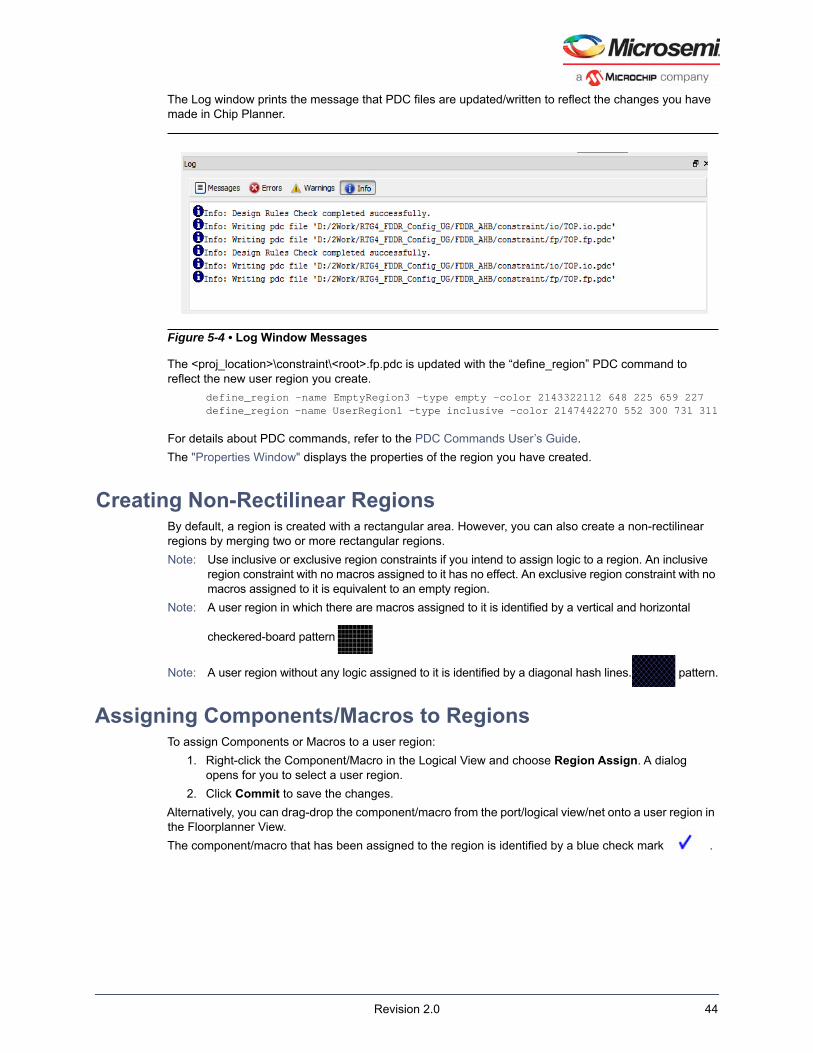
The Log window prints the message that PDC files are updated/written to reflect the changes you have made in Chip Planner.
The <proj_location>\constraint\<root>.fp.pdc is updated with the “define_region” PDC command to reflect the new user region you create.
define_region -name EmptyRegion3 -type empty -color 2143322112 648 225 659 227define_region -name UserRegion1 -type inclusive -color 2147442270 552 300 731 311
For details about PDC commands, refer to the PDC Commands User’s Guide. The "Properties Window" displays the properties of the region you have created.
Creating Non-Rectilinear RegionsBy default, a region is created with a rectangular area. However, you can also create a non-rectilinear regions by merging two or more rectangular regions. Note: Use inclusive or exclusive region constraints if you intend to assign logic to a region. An inclusive
region constraint with no macros assigned to it has no effect. An exclusive region constraint with no macros assigned to it is equivalent to an empty region.
Note: A user region in which there are macros assigned to it is identified by a vertical and horizontal checkered-board pattern
Note: A user region without any logic assigned to it is identified by a diagonal hash lines. pattern.
Assigning Components/Macros to RegionsTo assign Components or Macros to a user region:
1. Right-click the Component/Macro in the Logical View and choose Region Assign. A dialog opens for you to select a user region.
2. Click Commit to save the changes. Alternatively, you can drag-drop the component/macro from the port/logical view/net onto a user region in the Floorplanner View.The component/macro that has been assigned to the region is identified by a blue check mark .
Figure 5-4 • Log Window Messages
Revision 2.0 44

The Log window prints the message that PDC files are updated/written to reflect the changes you have made in Chip Planner.The <proj_location>\constraint\<root>.fp.pdc is updated with the assign_region PDC command:
define_region -name UserRegion1 -type inclusive -color 2147442270 552 300 731 311assign_region UserRegion1 FDDR_INIT_0
For details about PDC commands, refer to the PDC Commands User’s Guide.
Routing Inside a Constrained RegionBy default, when a region is first created, the region properties (Inclusive/Exclusive/Empty) apply to design resources (Placement) only. The Place and Route tool is free to use the routing resources inside the region. To further constrain the Place and Route tool on routing resources usage inside the region, click the Constrain Routing checkbox in the Properties window.
Figure 5-5 • Macro Assigned to a User Region
Revision 2.0 45

Figure 5-6 • Constrain Routing Checkbox inside Property Window
Constrain RoutingThis option applies to all types of regions: inclusive, exclusive, and empty. When this checkbox is checked, the region constraints are applied to routing, in addition to placement. The routing behavior is summarized in Table 5-1 for each type of user region.
Table 5-1 • Routing Behavior Inside User Regions with Constrain Routing Enabled
Region Type Routing Behavior
Inclusive • For all nets internal to the region (the source and all destinations belong to the region), routing must be inside the region (that is, such nets cannot be assigned any routing resources that are outside the region or cross the region boundaries).
• Nets not internal to the region can use routing resources within the region.
Exclusive • For all nets internal to the region (the source and all destinations belong to the region), routing must be inside the region (that is, such nets cannot be assigned any routing resources that are outside the region or cross the region boundaries).
• Nets without pins inside the region cannot be assigned any routing resources that are outside the region or cross region boundaries).
Empty • No routing is allowed inside the Empty Region. • However, local clocks and globals can cross empty regions.
Revision 2.0 46

Empty Region General GuidelinesEmpty regions allow you to create exclusive areas on the device where no logic placement can occur. Empty regions help guide the placer to pack your logic closer together and thereby use more local routing resources to connect it. You cannot create empty regions in areas that contain locked macros. Use the following guidelines for empty regions.
Use Empty Regions to Guide the Place-and-Route ProcessIf your design does not completely use up your target device (for example, 60% utilization or lower), use empty regions to cluster your logic placement into specific subareas of the chip. This helps when you have originally placed-and-routed the design into a smaller device but want to fit it to a larger part while still preserving the performance you have achieved in the smaller device.
Use Empty Regions to Reduce Routing CongestionCreating empty regions next to the congested area(s) of your design helps reduce congestion. When you place an empty region next to congested logic blocks or regions, the placer cannot place any logic next to your region or logic block. Logic which would normally be placed there is forced to be placed somewhere else. Routing resources next to the congested area are freed up and provide the router more options to route signals into the congested block.Before deciding to place empty region(s), analyze your design for congestion areas. Use the Ratsnest view in Chip Planner to see dense areas of connectivity into and out of your logic blocks or regions. Create empty regions in these congested areas and see it if improves the routability of your logic.
Use Empty Regions to Reserve Device ResourcesIf you want to preserve the placement of your existing design but plan additional modifications in the future, create empty regions in the areas of the chip where you plan to add additional logic. As you add new logic, remove or resize your empty regions accordingly to fit your new logic. Empty regions placed over I/O pins reserve them for future use as the I/O needs of your design changes. There are some restrictions for using empty regions in this manner.
Overbooking of RegionsOverbooking of regions (assigning resources over 100% utilization) is not allowed. When you try to overbook a region, Chip Planner shows the overbooked resource type in the "Properties Window"of the Region and the resources are not assigned to the region. The overbooked resource is highlighted in red in the Region Properties window.
Figure 5-7 • Overbooking of Region
Revision 2.0 47

User Action in Regions in the Floorplanner ViewWhen you select a region on the Floorplanner View, you may see some of the options below:
• Rename Regions• Delete Regions• Merge Regions• Unassign macros from Regions• Assign Macros inside Region• Clone Region• Unassign All• Unassign Selected Nets• Unassign Selected Components• Unassign Selected Ports
Note: The Floorplanner View has two modes of operation: Macro Manipulation Mode and Region Manipulation Mode. If the Floorplanner View is in the Macro Manipulation Mode, before any region operations (Resizing/Renaming/Deleting/Merging), you must first click the Region Manipulation Mode button to enter the Region Manipulation Mode.
Note: Any side-effects, such as unplacing or unassigning of a macro due to region creation or region resizing, are shown in the Log window.
Revision 2.0 48

6 – Netlist Views
In addition to the chip view for floorplanning purposes, Chip Planner displays (in the same Floorplanner View window) a schematic view of the design to make it easier to trace nets and debug the design.Two netlist types can be displayed in the Floorplanner View window:
• Post-Synthesis Hierarchical View (Hierarchical NLV) • Post-compile flattened Netlist View (Flat NLV)
The Floorplanner View and the Netlist Views are identified by tabs across the top of the window after they are loaded into memory. This makes it easy to switch between the different views.
Hierarchical NLV View The Post-Synthesis Hierarchical View (Hierarchical NLV) is a hierarchical view of the netlist after synthesis and after technology mapping to the Microsemi FPGA technology. Click the Hierarchical NLV button to display this view. Chip Planner loads the netlist into the system memory and displays it in the Floorplanner View window.When the netlist is loaded for the first time into memory, a pop-up progress bar indicates the progress of the loading process, which may incur some runtime penalty for a large netlist.
Flat NLV View This is the flattened (non-hierarchical) netlist generated after synthesis, technology mapping and further optimization based on the DRC rules of the device family and/or die. Click the Flat NLV button to display this view. Chip Planner loads the netlist into the system memory and displays it in the Floorplanner View window.
Figure 6-1 • Hierarchical NLV View
Revision 2.0 49

When the netlist is loaded for the first time into memory, a pop-up progress bar indicates the progress of the loading process, which may incur some runtime penalty for a large flattened netlist.
Display Across Multiple PagesHierarchical or flattened netlists may span across multiple pages, in which case the first page is displayed when it opens.The current page number and the total number of pages are displayed in the status bar at the lower right corner of the window.
To go to different pages of the Netlist view, use the left-pointing arrow or right-pointing arrow .
Netlist Viewer FeaturesSee the Netlist Viewer Interface User Guide for details on the Netlist Viewer features.
Figure 6-2 • Flat NLV - Flattened Netlist
Figure 6-3 • Status Bar
Revision 2.0 50

7 – Cross-Probing from SmartTime to Chip View/Netlist View
Cross-probing allows you to select a design object in one application and see the selection reflected in another application. When you cross-probe a design object from SmartTime to the Chip View /Netlist View, you will understand better how the two applications interact with each other.
Cross-probing from SmartTime to Chip View With cross-probing, a timing path not meeting timing requirements may be fixed with relative ease when you see the less-than-optimal placement of the design object (in terms of timing requirement) in Chip Planner. Cross-probing from SmartTime to Chip Planner is available for the following design objects:
• Macros• Ports• Nets/Paths
Note: Cross-probing of design objects is available from SmartTime to Chip Planner but not vice versa.Before you can cross-probe from SmartTime to Chip Planner, you must:
1. Complete Place and Route on the design.2. Open both SmartTime and Chip Planner.
Cross-Probing ExamplesTo cross-probe from SmartTime to Chip Planner, a design macro in the SmartTime is used as an example.
Design Macro Example1. Make sure that the design has successfully completed the Place and Route step.2. Open SmartTime Maximum/Minimum Analysis view.3. Open Chip Planner.4. In the SmartTime Maximum Analysis view, right-click the instance Q[2] in the Timing Path Graph
and choose Show in Chip Planner. With cross-probing, the Q[2] macro is selected in Chip Planner's Logical view (zoom in to see the selected item) and highlighted (white) in the Floorplanner View (zoom in to see the selected item). The Properties window in Chip Planner displays the properties of Q[2].
Note: The menu item Show in Chip Planner is grayed out if Chip Planner is not already open.
Revision 2.0 51

Note: You may need to zoom in to view the highlighted Q[2] Macro in the Floorplanner View.
Figure 7-1 • Cross-Probing the Q[2] Macro
Timing Path Example1. Make sure that the design has successfully completed the Place and Route step.2. Open SmartTime Maximum/Minimum Analysis view.3. Open Chip Planner.4. In the SmartTime Maximum/Minimum Analysis view, right-click the net Cliburn/U0/
U_IOPAD:PAD in the Table and choose Show Path in Chip Planner. Note that the net is selected (highlighted in red) in the Floorplanner View and the three macros connected to the net are also highlighted (white) in the Floorplanner View.
Revision 2.0 52

Note: The menu item Show Path in Chip Planner is grayed out if Chip Planner is not already open
Figure 7-2 • Cross-Probing - Timing Path
.
Alternatively, right-click from SmartTime’s Max/Min Delay Analysis Table view to cross-probe into Chip Planner.
Port Example1. Make sure that the design has successfully completed the Place and Route step.2. Open the SmartTime Maximum/Minimum Analysis view. 3. Open Chip Planner.4. In the SmartTime Maximum/Minimum Analysis view, right-click the port CLK in the Path and
choose Show in Chip Planner. Note that the port “CLK” is selected and highlighted in Chip Planner's Port view.
Figure 7-3 • Cross-Probing from Max/Min Delay Analysis View Table
Revision 2.0 53

Note: The menu item Show in Chip Planner is grayed out if Chip Planner is not already open.
Figure 7-4 • Cross-Probing - Port
From the Properties view inside Chip Planner, you will find useful information about the Port “CLK” you are cross-probing:
• Port Type• Port Placement Location (X-Y Coordinates)• I/O Bank Number• I/O Standard• Pin Assignment
Cross-probing from Chip Planner to Netlist ViewerTo cross-probe from Chip Planner to the Netlist Viewer (Flat NLV only):
1. Open Chip Planner and load the Flat NLV into Netlist Viewer.2. Select the design object in Chip Planner: Ports in Port Tab, Macros in Logical Tab and
Nets in Net Tab.
Revision 2.0 54

Figure 7-5 shows the Port PRDATA[22] selected in the Logical tab and highlighted in the etlist Viewer.
Cross-probing from SmartTime to Netlist ViewerCross-probing from SmartTime to Netlist Viewer allows you to examine and debug timing-critical paths as the first step towards timing closure. Timing paths with setup or hold time violations can be selected and cross-probed from SmartTime to Netlist Viewer to examine how the net is routed. Cross-probing may reveal and identify routing congestions.
To cross-probe a net from SmartTime to Netlist Viewer:
1. Complete the Place-and-Route step.2. Open Chip Planner.3. Load the Flattened AFL Netlist into Netlist Viewer.4. Open SmartTime in the Design Flow window.5. Open the Maximum/Minimum Delay Analysis View.6. Click on a timing path to open the Timing Path display in SmartTime.7. Right-click a net in the timing path display or a timing path in the SmartTime table and
select Show in Chip Planner.
Figure 7-5 • Cross-probe from Chip Planner to Netlist Viewer
Revision 2.0 55

Netlist Viewer opens a Logical Cone View to display the selected path and highlight it (Figure 7-7).
Figure 7-6 • Cross-Probe From SmarTime to NelistViewer
Figure 7-7 • Cross-Probed Net in Netlist Viewer Logical Cone View
Revision 2.0 56

8. If desirable, add Drivers or Loads to the net in the Netlist Active Cone view for debugging.
Note: The cone view may not show the path’s input IO or some extra macros along the path added by the Flattened View(but not shown in the SmartTime Path). To get a complete path in the Logical Cone View, double click the dashed net or right-click > add driver/load to cone.
Revision 2.0 57

A - Limitations
This appendix lists Chip Planner limitations:
I/O Register Support Every I/O has several embedded registers that you can use for faster clock-to-out timing, and to meet external hold and setup timing requirements. This feature uses input, output, or enable registers available in the I/O block. However, a register (if combined with an I/O register) is not shown in the Logical view as a separate element, and is shown as part of a port.
Figure B-1 • Register Combined with Input Register of an I/O
Internal Elements of External IP Macros Displayed in a Single Connection
Some external IP, such as SERDES and FDDR, span across multiple clusters and have their own dedicated ports. However, the net connected to these macro I/Os are shown to be connected from a single location. Figure B-2 is an example of a SERDES macro which shows all the associated nets connected to a single macro.
Revision 2.0 58

Figure B-2 • SERDES Macro with Associated Nets in a Single Connection
Cross-probing into SmartTime UnavailableCross-probing from the Chip View /Netlist View into SmartTime is not available. Cross-probing is supported for SmartTime to Chip View/Netlist View but not vice versa.
Revision 2.0 59