Embed Size (px)
Citation preview
Leica EBPG5000 Series
Electron Beam Lithography Systems
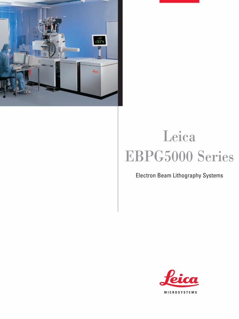
Leica Microsystems-Your DedicatedPerformance Partner!
Leica has a 30-year record of successful design, manufacture and
supply of Electron Beam Lithography Tools. During this period
over 200 systems have been installed and supported in more than
25 different countries worldwide. Today, Leica Microsystems
Lithography is providing leading edge technology solutions in all
areas of advanced lithography, both in the manufacturing roles of
direct write & maskwriting as well as the key enabling nanolitho-
graphy role for research and development.
All of these applications are addressed with systems that are
characterized by their state of the art resolution, accuracy and
throughput as well as extensive software control. They deliver wide
application versatility combined with ease of use. Our dedicated
field service, training and support teams and our established upg-
rade policy ensure that the value of customers’ investments is
maintained over a long productive system life.
2
3
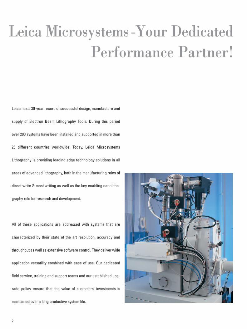
The latest Leica EBPG5000 Series Beamwriter systems continue
the evolution of this highly respected and field proven Gaussian
beam – vector scan product. Improved application functionality
and operational specifications have been defined and developed
from the wide range of dedicated user feedback. This has enabled
Leica to create very specific solutions to some of the most
demanding patterning requirements of the widely experienced
Beamwriter community.
These nano-resolution tools provide a cost effective solution to
many of today’s sub-100nm lithography needs in a proven and
productive package.
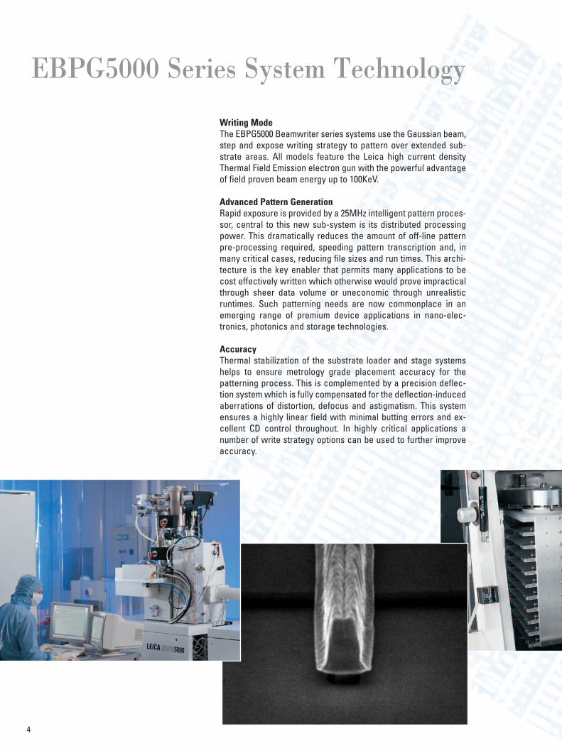
Writing ModeThe EBPG5000 Beamwriter series systems use the Gaussian beam,step and expose writing strategy to pattern over extended sub-strate areas. All models feature the Leica high current densityThermal Field Emission electron gun with the powerful advantageof field proven beam energy up to 100KeV.
Advanced Pattern GenerationRapid exposure is provided by a 25MHz intelligent pattern proces-sor, central to this new sub-system is its distributed processingpower. This dramatically reduces the amount of off-line patternpre-processing required, speeding pattern transcription and, inmany critical cases, reducing file sizes and run times. This archi-tecture is the key enabler that permits many applications to becost effectively written which otherwise would prove impracticalthrough sheer data volume or uneconomic through unrealisticruntimes. Such patterning needs are now commonplace in anemerging range of premium device applications in nano-elec-tronics, photonics and storage technologies.
AccuracyThermal stabilization of the substrate loader and stage systemshelps to ensure metrology grade placement accuracy for thepatterning process. This is complemented by a precision deflec-tion system which is fully compensated for the deflection-inducedaberrations of distortion, defocus and astigmatism. This systemensures a highly linear field with minimal butting errors and ex-cellent CD control throughout. In highly critical applications anumber of write strategy options can be used to further improveaccuracy.
EBPG5000 Series System Technology
4
5
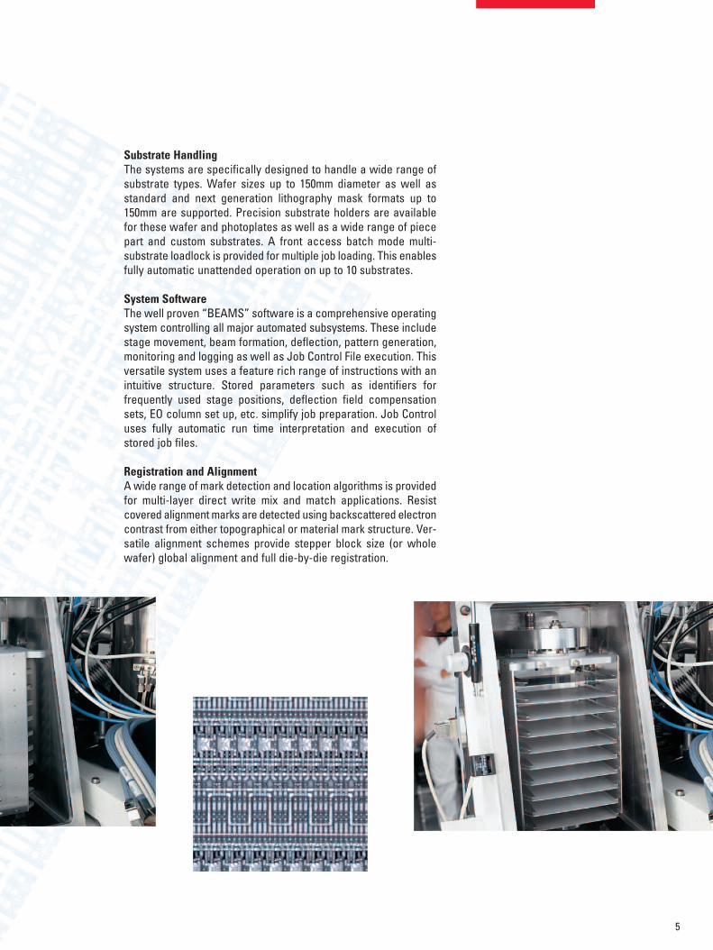
Substrate HandlingThe systems are specifically designed to handle a wide range ofsubstrate types. Wafer sizes up to 150mm diameter as well asstandard and next generation lithography mask formats up to150mm are supported. Precision substrate holders are availablefor these wafer and photoplates as well as a wide range of piecepart and custom substrates. A front access batch mode multi-substrate loadlock is provided for multiple job loading. This enablesfully automatic unattended operation on up to 10 substrates.
System SoftwareThe well proven “BEAMS” software is a comprehensive operatingsystem controlling all major automated subsystems. These includestage movement, beam formation, deflection, pattern generation,monitoring and logging as well as Job Control File execution. Thisversatile system uses a feature rich range of instructions with anintuitive structure. Stored parameters such as identifiers forfrequently used stage positions, deflection field compensationsets, EO column set up, etc. simplify job preparation. Job Controluses fully automatic run time interpretation and execution ofstored job files.
Registration and AlignmentA wide range of mark detection and location algorithms is providedfor multi-layer direct write mix and match applications. Resistcovered alignment marks are detected using backscattered electroncontrast from either topographical or material mark structure. Ver-satile alignment schemes provide stepper block size (or wholewafer) global alignment and full die-by-die registration.
6
7
Advanced compound semiconductor microwave devices havelong required accurately controlled gate structures down to 100 nmCD or less. In addition they demand the added complexity of “T”shaped (or other profile) cross-section in order to deliver adequategate conductance with low gate capacitance. The larger geometrysource/drain metalization layer of such devices is typicallypatterned using lower cost optical systems. These typically sufferfrom stepper lens distortions, which further complicates achievinggood overlay accuracy when using a mix and match of tools.
These demanding gate level requirements are being very success-fully addressed using Leica e-beam lithography systems. Over 25such Leica units are currently in use worldwide for this applicationboth in full manufacturing and R&D/Prototyping roles. They deliverprofitable manufacturing throughput as well as CD resolution,control and overlay accuracy to satisfy the most demanding R&Drequirements.
Leica EBPG5000 Series systems have many unique characteristicswhich have led to their wide adoption in this role. Their reliable,high brightness 100keV TFE electron source minimizes exposuretime and delivers a stable high precision writing beam. Through-put is further improved by the low mass, fast stepping stage whichgreatly reduces non-exposure overhead times compared withunnecessarily large stage system tools.
Manufacturing & PrototypingApplications
8

9
Programmable exposure dosage of individual pattern features inreal-time is used with multi-layer resists to provide the criticaldeveloped resist profile suitable for “clean” lift-off metalizationwith good process latitude.
The extensively proven operating software suite “BEAMS” providesmany overlay accuracy enhancing facilities. It has the benefit ofmany years of user feedback and offers versatile mark detectionalgorithms with a range of “Die by die” or “cluster alignment”overlay strategies. These provide the necessary sub 30 nm gatealignment even in the presence of quite distorted base layerpatterning.
These are some of the many user-appreciated qualities of theBeamwriter systems but there are many more specific EBPG5000Series benefits which this latest series provides.
Much greater depth of focus, freedom from planarization restric-tions, ease in producing contoured resist profiles and structureperiodicity set to fractions of a nanometer are all inherent capa-bilities that can become compelling application solutions.
Wide application versatility has been one of the most importantdesign criteria in the evolution of the EBPG5000 Series. Thesuccess of this goal is clearly evident in the diversity of the userbase. Research and Development patterning for CMOS andmicrowave devices, Quantum Functional Devices, Photonic ele-ments, and a variety of NGL mask technologies are all currentroutine applications for Beamwriter systems.
In addition many other novel high resolution structures necessaryfor emerging nano-electronics, optics, nano electromechanicalsystems, and biological/medical devices have been successfullypatterned. These more “exotic” devices often require patterningon non-semiconductor industry substrates with a wide diversityof material types, irregular shape and non-planar imaging surfaces.The EBPG5000 is well matched and configured for all of theseapplications.
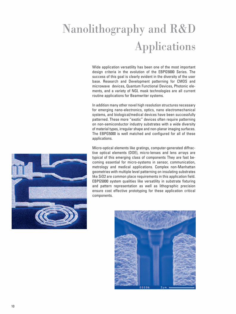
Micro-optical elements like gratings, computer-generated diffrac-tive optical elements (DOE), micro-lenses and lens arrays aretypical of this emerging class of components They are fast be-coming essential for micro-systems in sensor, communication,metrology and medical applications. Complex non-Manhattangeometries with multiple level patterning on insulating substrateslike SiO2 are common place requirements in this application field.EBPG5000 system qualities like versatility in substrate fixturingand pattern representation as well as lithographic precisionensure cost effective prototyping for these application criticalcomponents.
Nanolithography and R&DApplications
10

11
Sensor and actuator devices using nano-electromechanicaltechniques are another application field for Beamwriter systems.They are used to define such diverse components as a magnet-izing coil/nano-Hall probe combination at the tip of an AFM probeand biological nano-blood sensors.
Resolution, accuracy and versatility are also the main reasonswhy EBPG5000 Series systems are relied on to prototype lowdimensional silicon device structures. Such quantum functionaldevices now provide the promise of continuing levels of integra-tion beyond that considered feasible with conventional semicon-ductor device structures.
Leica EBPG5000 Series systems offer the most cost effectivesystem of choice for many of today’s R&D lithographic needs.Beamwriter systems are in use at many of the world’s mostadvanced industrial companies. They are also placed in many ofthe world’s leading government and academic research labo-ratories, providing solutions for a wide variety of lithographicrequirements in many diverse application fields. Such versatilitystems from the continuing success of a hardware and softwareplatform that has truly field proven credentials.
To find out more detailed information on how the EBPG5000 Seriesproducts can help solve your advanced lithography requirementsplease contact your nearest Leica Microsystems office as listedoverleaf.
Copy
right
©Le
ica
Mic
rosy
stem
s Li
thog
raph
y Lt
d. •
Clift
on R
oad
•Ca
mbr
idge
CB1
3QH
•Un
ited
King
dom
200
3 •
phon
e +4
4 1
223
411
123
•fa
x +4
4 1
223
249
678
LEI
CA a
nd th
e Le
ica
Logo
are
regi
ster
ed tr
adem
arks
of L
eica
IR G
mbH
.En
glis
h 10
0123
8 • P
rinte
d on
chl
orin
e-fre
e bl
each
ed p
aper
. V
III/0
3/FX
/K.H
.
@www.semiconation.com
Leica Microsystems –the brand for outstanding productsLeica Microsystems’ mission is to be the world’s first-choice provider of innovativesolutions to our customers’ needs for vision, measurement, lithography and analysisof microstructures.
Leica, the leading brand for microscopes and scientific instruments, developed fromfive brand names, all with a long tradition: Wild, Leitz, Reichert, Jung and CambridgeInstruments. Yet Leica symbolizes innovation as well as tradition.
Leica Microsystems – an international companywith a strong network of customer services
The Semiconductor Equipment Division
Asia PacificTaiwan, Taiwan, R.O.C. phone: +886 3 523 5777 fax: + 886 3 523 5778
EuropeMicroelectronic Inspection & Metrology EquipmentGermany, Wetzlar phone: +49 6441 292516 fax: +49 6441 292395
Shaped Beam Lithography SystemsGermany, Jena phone: +49 3641 651902 fax: +49 3641 651922
Gaussian Beam Lithography SystemsUnited Kingdom, Cambridge phone: +44 1 223 411 123 fax: +44 1 223 249 678
JapanJapan, Tokyo phone: +81 3 5435 9600 fax: +81 3 5435 9615
KoreaKorea, Seoul phone: +82 2 3416 4520 fax: +82 2 514 6548
North AmericaUSA, Chantilly phone: +1 800 909 3935 fax: +1 703 229 4535
and representatives of Leica Microsystemsin more than 100 countries.
The companies of the Leica MicrosystemsGroup operate internationally in five businesssegments, where we rank with the marketleaders.
• MicroscopyOur expertise in microscopy is the basis for allour solutions for visualization, measurementand analysis of microstructures in life sciencesand industry.
• Specimen PreparationWe specialize in supplying complete solutionsfor histology and cytopathology.
• Imaging SystemsWith confocal laser technology and imageanalysis systems, we provide three-dimensionalviewing facilities and offer new solutions forcytogenetics, pathology and materials sciences.
• Medical EquipmentInnovative technologies in our surgical micro-scopes offer new therapeutic approaches inmicrosurgery. With automated instruments forophthalmology, we enable new diagnosticmethods to be applied.
• Semiconductor EquipmentOur automated, leading-edge measurement andinspection systems and our E-beam lithographysystems make us the first choice supplier forsemiconductor manufacturers all over the world.


![KR Leica Builder Series Brochure[1]](https://img.pdfslide.us/doc/110x75/577d20291a28ab4e1e921f4b/kr-leica-builder-series-brochure1.jpg)