Embed Size (px)
Citation preview

Lecture no 2 to 5
THE BASIC BJT AMPLIFIER CONFIGURATIONS
Prepared by Engr:Sarfaraz Khan Turk
Lecturer at IBT LUMHS Jamshoro

Basic BJT Amplifiers Circuits
Single-Stage BJT Amplifiers
Key Words: Common-Emitter Amplifier Graphical Analysis Small-Signal Models Analysis Common-Collector Amplifier Common-Base Amplifier

Basic BJT Amplifiers CircuitsSingle-Stage BJT Amplifiers
C-E Amplifiers
To operate as an amplifier, the BJT must be biased to operate in active mode and then superimpose a small voltage signal vbe to the base.
oC
CER
cii
BBEC
i vviivv CBC 12
DC + small signal
OC vi Bi iv CB ii
coupling capacitor (only passes ac signals)

Basic BJT Amplifiers Circuits
Single-Stage BJT Amplifiers
C-E Amplifiers
iV
iV
Vi
+
iV

Basic BJT Amplifiers Circuits
Single-Stage BJT Amplifiers
C-E Amplifiers
vBE=vi+VBE
bBB iIi
Apply a small signal input voltage and see ib

Basic BJT Amplifiers Circuits
Single-Stage BJT Amplifiers
C-E Amplifiers
• vi = 0 IB 、 IC 、 VCE
ceCECE
CCC
bBBi
vVv
iIi
iIiv 0
)()( ioiMoM ffVV •
• vo out of phase with vi
iC=ic+IC
vCE=vce+VCE
See how ib translates into vce.

BJT Amplifiers Circuits
Single-Stage BJT Amplifiers
C-E Amplifiers Considering (all the capacitors are replaced by open circuits)
CV
Considering (all the capacitors are replaced by short circuits)
iV

Basic BJT Amplifiers Circuits
Single-Stage BJT Amplifiers
C-E AmplifiersConsidering (all the capacitors are replaced by open circuits)
CV
Considering (all the capacitors are replaced by short circuits)
iV

Basic BJT Amplifiers Circuits
Single-Stage BJT AmplifiersGraphical Analysis
VCC
• Can be useful to understand the operation of BJT circuits.• First, establish DC conditions by finding IB (or VBE)• Second, figure out the DC operating point for IC
Can get a feel for whether the BJT will stay in active region of operation – What happens if RC is larger or smaller?

Basic BJT Amplifiers CircuitsSingle-Stage BJT Amplifiers
Graphical Analysis
VCC
')//( LcLCcce RiRRiv

Basic BJT Amplifiers Circuits
Single-Stage BJT Amplifiers
Graphical Analysis
Q-point is centered on the ac load line:
VCC

VCC
Basic BJT Amplifiers Circuits
Single-Stage BJT Amplifiers
Graphical Analysis
Clipped at cutoff(cutoff distortion)
Q-point closer to cutoff:

VCC
Basic BJT Amplifiers Circuits
Single-Stage BJT Amplifiers
Graphical Analysis
Clipped at cutoff(saturation distortion)
Q-point closer to saturation:

Basic BJT Amplifiers CircuitsSingle-Stage BJT Amplifiers
Graphical Analysis

Basic BJT Amplifiers Circuits
Single-Stage BJT Amplifiers
Small-Signal Models Analysis
Steps for using small-signal models1. Determine the DC operating point of the BJT - in particular, the collector current2. Calculate small-signal model parameters: rbe
3. Eliminate DC sources – replace voltage sources with short circuits and current sources with open circuits4. Replace BJT with equivalent small-signal models5. Analysis

Basic BJT Amplifiers Circuits
Single-Stage BJT Amplifiers
Small-Signal Models Analysis
IC ≈ βIB,
IE = IC + IB = (1+β)IB
eEBEbBCBC RIVRIR)II(V
))(1( eb
BECB RRR
VVI
)( eECCCCE RRIRIVV
Example 1

Basic BJT Amplifiers Circuits
Single-Stage BJT Amplifiers
Small-Signal Models Analysis
Example 2
vs
CCbb
bB V
RR
RV
21
2
eBe
BEBEC RV
R
VVII /
C
B
II
)RR(IVV eCCCCCE
Basic BJT Amplifiers Circuits
Single-Stage BJT Amplifiers
Small-Signal Models Analysis
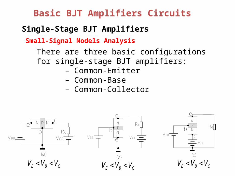
There are three basic configurations for single-stage BJT amplifiers: – Common-Emitter – Common-Base – Common-Collector
VBB VCCRC
NN P ce
b
(a)
VBB VCC
RcN
NP
c
e
b
(b)
VBB
VCC
Re
N
NP
c
e
b
(c)
E B CV V V E B CV V V E B CV V V

Basic BJT Amplifiers Circuits
Single-Stage BJT Amplifiers
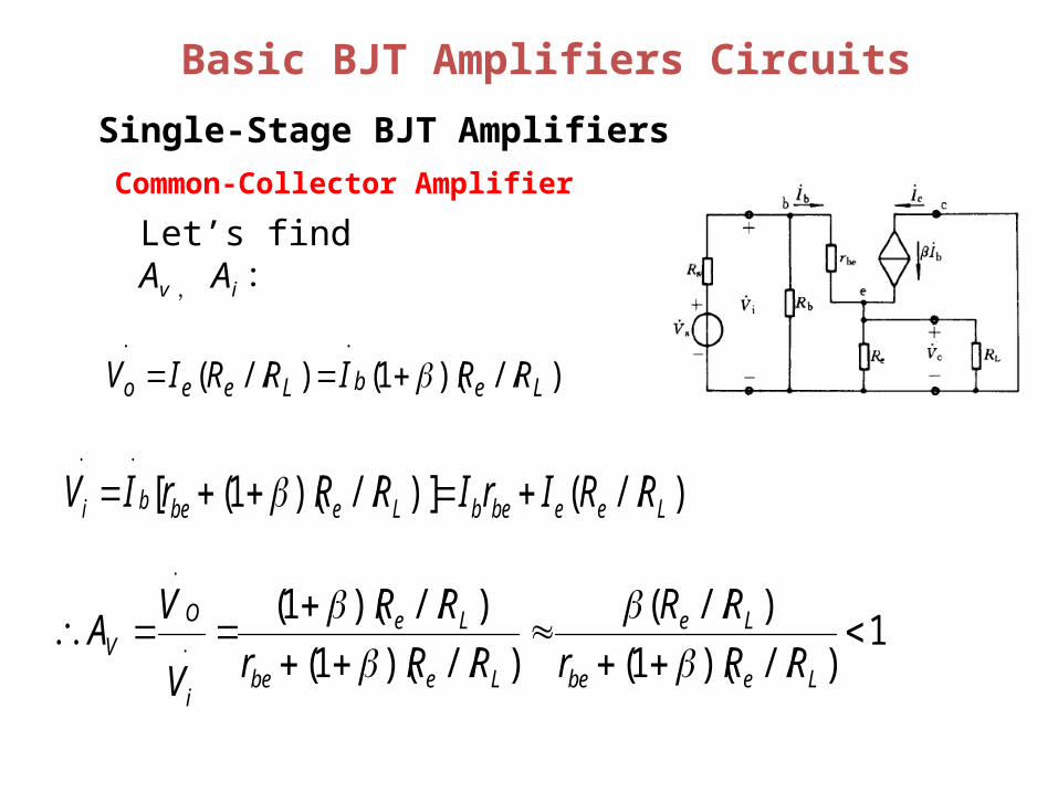
Common-Collector Amplifier
eEBEbBCC RIVRIV eBBEbB RIVRI )1(
eb
CC
eb
BECCB RR
V
RR
VVI
1)1(
BC II
eCCEeECECC RIVRIVV
eCCCCE RIVV
(a) 共集电极电路
Note : is slightly less than due to the voltage drop introduced by
oV iV BEV
1VA

Basic BJT Amplifiers Circuits
Single-Stage BJT Amplifiers
Common-Collector Amplifier
(a) 共集电极电路
The last basic configuration is to tie the collector to a fixed voltage, drive an input signal into the base and observe the output at the emitter.
Basic BJT Amplifiers Circuits
Single-Stage BJT Amplifiers
Common-Collector Amplifier
)//()]//)(1([ LeebebLebebi RRIrIRRrIV
)//)(1()//( LebLeeo RRIRRIV
1)//)(1(
)//(
)//)(1(
)//)(1(
Lebe
Le
Lebe
Le
i
O
V RRr
RR
RRr
RR
V
VA
Let’s find Av ,
Ai :

Basic BJT Amplifiers CircuitsSingle-Stage BJT Amplifiers
Common-Collector Amplifier
bbiLebeb RIIRRrI )())//)(1((
b
bLeb
b
bLebebi R
RRRI
R
RRRrII
)//)(1()//)(1(
L
Lebo R
RRII
)//)(1(
bLe
b
L
Lei RRR
R
R
RRA
)//)(1(
)//)(1(
L
Le
R
RR )//)(1(
)//)(1( Le RR << Rb
iAL
Le
R
RR )//)(1( >>1
Let’s find Av ,
Ai : )//()1()//( LebLeeLo RRIRRIRI oI
iI

Basic BJT Amplifiers Circuits
Single-Stage BJT Amplifiers
Common-Collector Amplifier
Ri
)//)(1()//( LebebLeebebi RRriRRiriv
b
ii i
vR )//)(1( Lebe RRr
)//(////)]//)(1([// LebbLebebii RRRRRRrRRR
Let’s find Ri :

Basic BJT Amplifiers Circuits
Single-Stage BJT Amplifiers
Common-Collector Amplifier
Ro
(b)
I
IRe
Let’s find Ro :
bb IIII Re
)1()//(11
1
bsbee
o
RRrRi
vR
Re eI I I Re eI I I
1Re e Re bI I I I I
bsbee RRr
v
R
v
//)1(
1
)//(// bsbe
e
RRrR
IeI
ReI
Basic BJT Amplifiers Circuits
Single-Stage BJT Amplifiers
Common-Collector Amplifier
Ro
(b)
I
IRe
Ri (a)
bLebei RRRrR //)]//)(1([
1
)//(// bsbe
eoRRr
RR

Basic BJT Amplifiers Circuits
Single-Stage BJT Amplifiers
Common-Collector Amplifier
bLebei RRRrR //)]//)(1([
1
)//(// bsbe
eoRRr
RR
C-C amp characteristics:• Voltage gain is less than unity, but close (to unity) since β is large and rbe is small.• Also called an emitter follower since the emitter follows the input signal.• Input resistance is higher, output resistance is lower. - Used for connecting a source with a large Rs to a load with low resistance.
(a) 共集电极电路
1)//)(1(
)//(
Lebe
Le
i
O
V RRr
RR
V
VA
iAL
Le
R
RR )//)(1( >>1

Basic BJT Amplifiers Circuits
Single-Stage BJT Amplifiers
Common-Base Amplifier
(a) 共基极电路
Rc
2b2b1b
CCB R
RR
VV
eEBEB RIVV
e
B
e
BEBEC R
V
R
VVII
C
B
II )( eCCCCeECCCCCE RRIVRIRIVV
Ground the base and drive the input signal into the emitter

Basic BJT Amplifiers Circuits
Single-Stage BJT Amplifiers
Common-Base Amplifier
(a) 共基极电路 Ri
Ro
be
Lc
beb
Lccv r
RR
ri
RRiA
)//()//(
i
oi I
IA
1
)1(
)(
//)1(
)(
C
ELC
C
ebe
be
LC
C
I
IRRR
Rr
rRR
R
For RL<<RC, CEi IIA
since1)1(
e
be Rr
//)1( Ri=
Ro≈RC

Basic BJT Amplifiers Circuits
Single-Stage BJT Amplifiers
Common-Base Amplifier
(a) 共基极电路
be
Lcv r
RRA
)//(
i
oi I
IA
LC
CLC
C
RR
RRRR
)1(
)(
For RL<<RC, 1)1(
iA
)1(//
)1(
be
ebe r
Rr
Ri=
Ro≈R
C CB amp characteristics:• current gain has little dependence on β• is non-inverting• most commonly used as a unity-gain current amplifier or current buffer and not as a voltage amplifier: accepts an input signal current with low input resistance and delivers a nearly equal current with high output impedance• most significant advantage is its excellent frequency response

C-C C-E C-B
Input
Output
Functions
Summary for three types of diodes:
BI BIBI
EI CI CI
Basic BJT Amplifiers Circuits
Zout < Zin
Vout > Vin
Zout > Zin
Vout > VinVout ≈ Vin
Zout > Zin

Basic BJT Amplifiers Circuits
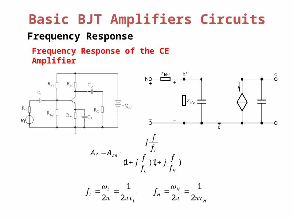
Frequency Response
Key Words: Basic Concepts High-Frequency BJT Model Frequency Response of the CE Amplifier

Basic BJT Amplifiers Circuits
Frequency Response
Basic Concepts
Time
0.5ms 1.0ms 1.5ms 2.0ms 2.5ms 3.0ms 3.5ms 4.0msV(1) V(2)
-1.0V
-0.5V
0V
0.5V
1.0V

Basic BJT Amplifiers Circuits
Frequency Response
Basic Concepts
Frequency0Hz 2KHz 4KHz 6KHz 8KHz 10KHz 12KHz 14KHz 16KHz 18KHz 20KHz
V(2) V(1)0V
200mV
400mV
600mV
800mV
Frequency
10Hz 100Hz 1.0KHz 10KHz 100KHz 1.0MHzV(2)
0V
0.5V
1.0V

Basic BJT Amplifiers CircuitsFrequency Response
Basic Concepts
Lower cut off frequency Upper cut off frequency
)()()()( vvv AAorffAA
The drops of voltage gain (output/input) is mainly due to:1 、 Increasing reactance of (at low f)2 、 Parasitic capacitive elements of the network (at high f)3 、 Dissappearance of changing current (for transformer coupled amp.)
ecs CCC ,,

Basic BJT Amplifiers Circuits
Frequency Response
C
C
In BJTs, the PN junctions (EBJ and CBJ) also have capacitances associated with them
rbe
C
C
C'rbe C'
High-Frequency BJT Model

Basic BJT Amplifiers Circuits
vs
Frequency Response
Frequency Response of the CE Amplifier
C'rbe C'
There are three capacitors in the circuit.
At the mid frequency band, these are considered to be short circuits and internal capacitors and are considered to be open circuits.
C',C'

Basic BJT Amplifiers Circuits
vs
Frequency Response
Frequency Response of the CE Amplifier
At low frequencies, C1, C2 are an open circuit and the gain is zero. Thus C1 has a high pass effect on thegain, i.e. it affects the lower cutoff frequency of the amplifier.
)////( 2111 bebbs rRRRC
2 is the time constant for C2. 12 ---is neglected
11 2
1
Lf

Basic BJT Amplifiers Circuits
vs
Frequency Response
Frequency Response of the CE Amplifier
)////( 2111 bebbs rRRRC
12 ---is neglected
Capacitor Ce is an open circuit. The pole time constant is given by the resistance multiplied by Ce.
eebesb
e CRrRR
//1
)//(
222
211.1 LeLLL ffff
eLef
2
1

C'rbe C'
Basic BJT Amplifiers CircuitsFrequency Response
Frequency Response of the CE Amplifier
vs
At high frequencies, C1, C2 Ce are all short circuit. The frequency that dominates is thelowest pole frequency.
The time constant is neglected for)1( '
CjRL C'
CrRR besbC )////(
C
Hf
2
1
In summary:the lower cut off frequency is determined by network capacitence. e.g. The higher cut off frequency is determined by the parasitic ferquency of the BJT. e.g.
C
eCCC ,21

C'rbe C'
Basic BJT Amplifiers CircuitsFrequency Response
Frequency Response of the CE Amplifier
vs )1)(1(HL
Lvmv
f
fj
f
fj
f
fj
AA
frequency-mid0,, —vmv
HLHL AA
f
f
f
ffffFor
frequency-low1
,0),( —
L
Lvmv
HHL
ff
j
ff
jAA
f
fffffFor
frequencyHigh
ff
jAA
f
fffffFor
H
vmvL
LH
—1
1,0)(
Basic BJT Amplifiers CircuitsFrequency Response
vs
)1)(1(HL
Lvmv
f
fj
f
fj
f
fj
AA
H
HH
L
LL ff
2
1
22
1
2
C'rbe C'
Frequency Response of the CE Amplifier

Basic BJT Amplifiers CircuitsFrequency Response
decadedecade
0
Frequency Response of the CE Amplifier

For student References.
Chapter 9 amplifier fundamentals (9.1) (9.2) from the book Electronic devices, circuit and systems (Micheal M cirovic)
Chapter 8 introduction to amplifiers (8.1) (8.2) from the book introductory electronic devices and circuits by author (Robert T .paynter).
Wikipedia and world wide web