Embed Size (px)
Citation preview
Department of Mechanical Engineering
Piezoelectricity
Lecture 8-1
Department of Mechanical Engineering
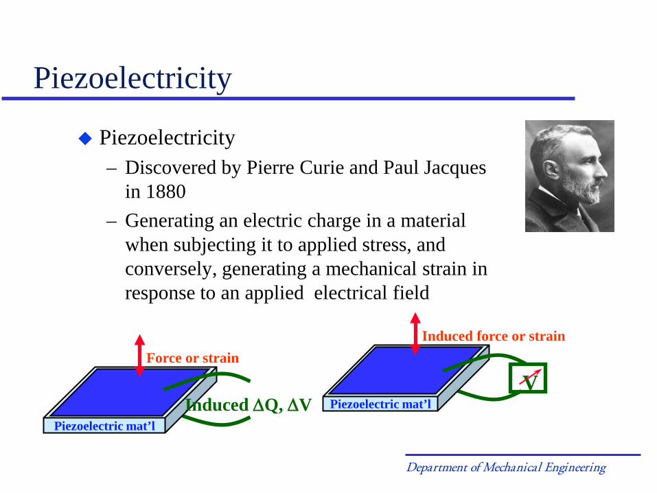
Piezoelectricity
Piezoelectricity– Discovered by Pierre Curie and Paul Jacques
in 1880– Generating an electric charge in a material
when subjecting it to applied stress, and conversely, generating a mechanical strain in response to an applied electrical field
Piezoelectric mat’l
Force or strain
Induced ∆Q, ∆V Piezoelectric mat’l
Induced force or strain
V
Department of Mechanical Engineering
Department of Mechanical Engineering
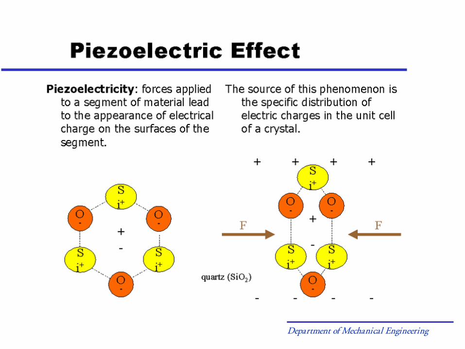
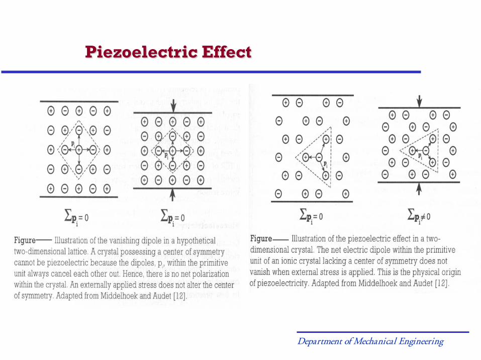
Piezoelectric Effect
Department of Mechanical Engineering
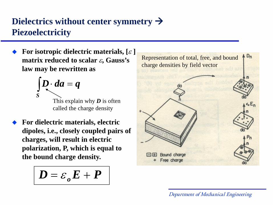
For isotropic dielectric materials, [ε ] matrix reduced to scalar ε, Gauss’s law may be rewritten as
Dielectrics without center symmetry Piezoelectricity
∫ =⋅S
qdaDThis explain why D is often called the charge density
For dielectric materials, electric dipoles, i.e., closely coupled pairs of charges, will result in electric polarization, P, which is equal to the bound charge density.
Representation of total, free, and bound charge densities by field vector
PED o += ε
Department of Mechanical Engineering
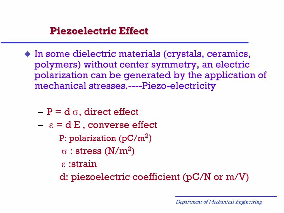
Piezoelectric Effect
In some dielectric materials (crystals, ceramics, polymers) without center symmetry, an electric polarization can be generated by the application of mechanical stresses.----Piezo-electricity
– P = d σ, direct effect– ε = d E , converse effect
P: polarization (pC/m2)σ : stress (N/m2)ε :straind: piezoelectric coefficient (pC/N or m/V)
Department of Mechanical Engineering
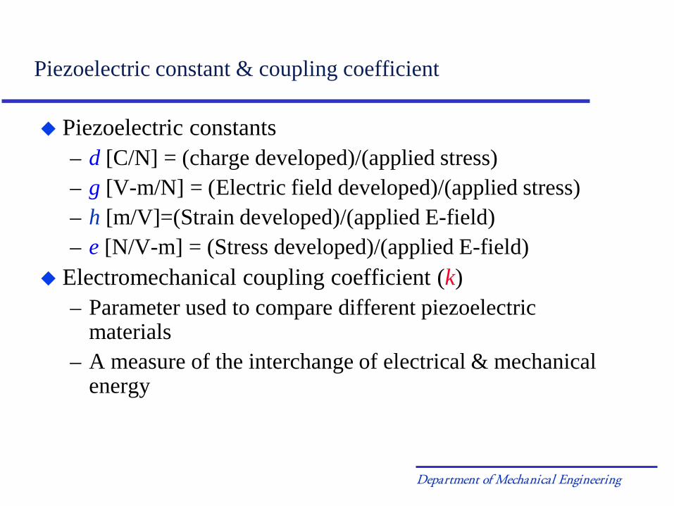
Piezoelectric constant & coupling coefficient
Piezoelectric constants– d [C/N] = (charge developed)/(applied stress) – g [V-m/N] = (Electric field developed)/(applied stress) – h [m/V]=(Strain developed)/(applied E-field)– e [N/V-m] = (Stress developed)/(applied E-field)
Electromechanical coupling coefficient (k)– Parameter used to compare different piezoelectric
materials– A measure of the interchange of electrical & mechanical
energy
Department of Mechanical Engineering
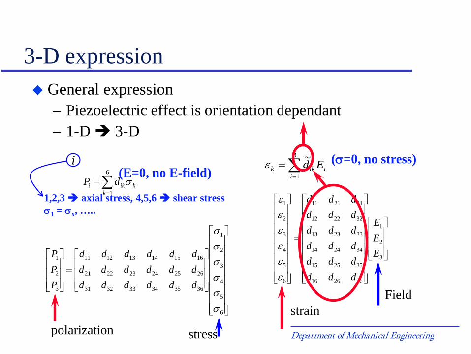
3-D expression General expression
– Piezoelectric effect is orientation dependant– 1-D 3-D
∑=
=6
1kkiki dP σ
(E=0, no E-field)
1,2,3 axial stress, 4,5,6 shear stress σ1 = σx, …..
=
6
5
4
3
2
1
363534333231
262524232221
161514131211
3
2
1
σσσσσσ
dddddddddddddddddd
PPP
∑=
=3
1
~i
iikk Edε (σ=0, no stress)
=
3
2
1
362616
352515
342414
332313
322212
312111
6
5
4
3
2
1
EEE
dddddddddddddddddd
εεεεεε
polarization stress
strainField
i
Department of Mechanical Engineering
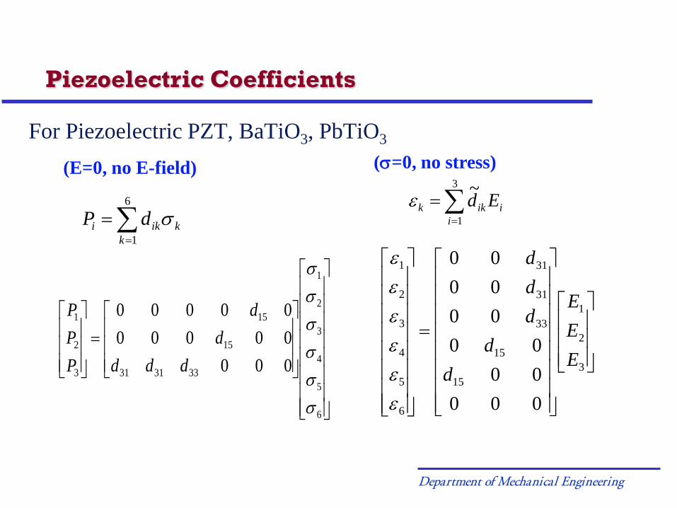
For Piezoelectric PZT, BaTiO3, PbTiO3
∑=
=3
1
~i
iikk Edε
(σ=0, no stress)
=
3
2
1
15
15
33
31
31
6
5
4
3
2
1
0000000
000000
EEE
dd
ddd
εεεεεε
∑=
=6
1kkiki dP σ
(E=0, no E-field)
=
6
5
4
3
2
1
333131
15
15
3
2
1
0000000000000
σσσσσσ
dddd
d
PPP
Piezoelectric Coefficients
Department of Mechanical Engineering
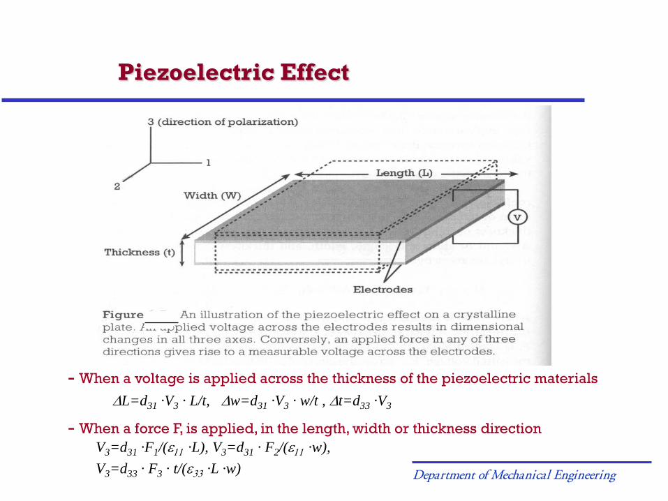
Piezoelectric Effect
∆L=d31 ·V3 · L/t, ∆w=d31 ·V3 · w/t , ∆t=d33 ·V3
- When a voltage is applied across the thickness of the piezoelectric materials
- When a force F, is applied, in the length, width or thickness directionV3=d31 ·F1/(ε11 ·L), V3=d31 · F2/(ε11 ·w), V3=d33 · F3 · t/(ε33 ·L ·w)

Department of Mechanical Engineering
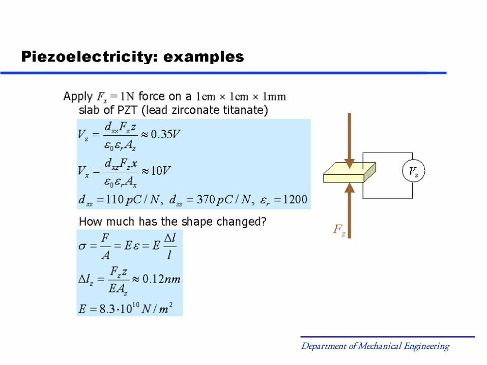
P=d σ
Open circuit voltage
Department of Mechanical Engineering
Department of Mechanical Engineering
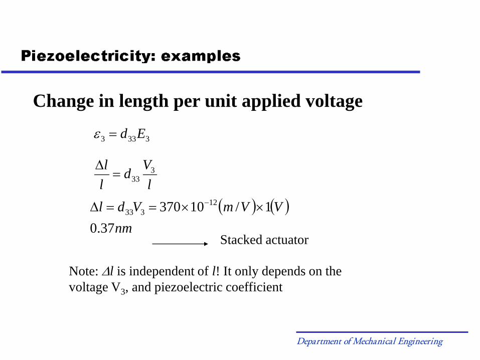
Change in length per unit applied voltage
3333 Ed=ε
lVd
ll 3
33=∆
( ) ( )nm
VVmVdl37.0
1/10370 12333 ××==∆ −
Note: ∆l is independent of l! It only depends on the voltage V3, and piezoelectric coefficient
Stacked actuator

Department of Mechanical Engineering
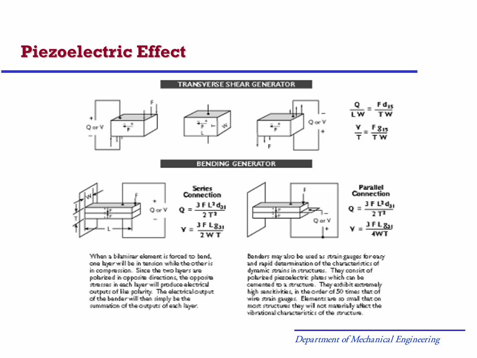
Piezoelectric Effect
HereT: thicknessF: applied force
Department of Mechanical Engineering
Piezoelectric Effect
Department of Mechanical Engineering
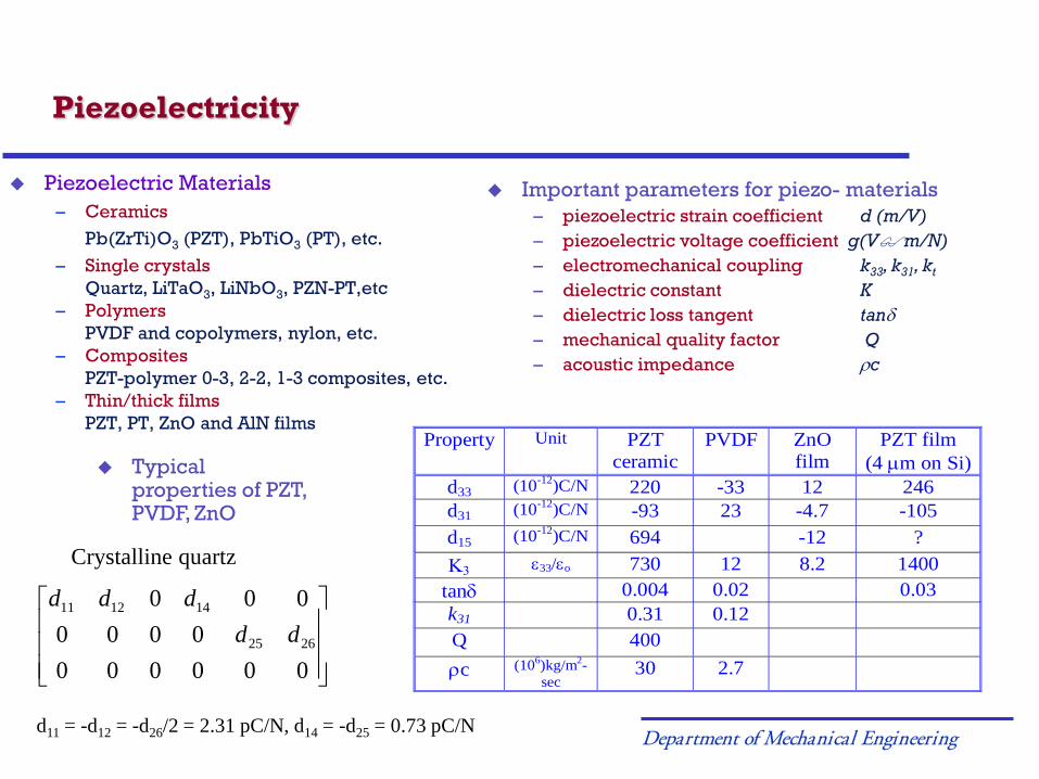
Piezoelectricity
Piezoelectric Materials– Ceramics
Pb(ZrTi)O3 (PZT), PbTiO3 (PT), etc.– Single crystals
Quartz, LiTaO3, LiNbO3, PZN-PT,etc– Polymers
PVDF and copolymers, nylon, etc.– Composites
PZT-polymer 0-3, 2-2, 1-3 composites, etc.– Thin/thick films
PZT, PT, ZnO and AlN films
Important parameters for piezo- materials– piezoelectric strain coefficient d (m/V)– piezoelectric voltage coefficient g(Vm/N)– electromechanical coupling k33, k31, kt
– dielectric constant K– dielectric loss tangent tanδ– mechanical quality factor Q– acoustic impedance ρc
Property Unit PZTceramic
PVDF ZnOfilm
PZT film(4 µm on Si)
d33 (10-12)C/N 220 -33 12 246d31 (10-12)C/N -93 23 -4.7 -105d15 (10-12)C/N 694 -12 ?Κ3 ε33/εo 730 12 8.2 1400
tanδ 0.004 0.02 0.03k31 0.31 0.12Q 400ρc (106)kg/m2-
sec30 2.7
Typical properties of PZT, PVDF, ZnO
Crystalline quartz
0000000000
000
2625
141211
ddddd
d11 = -d12 = -d26/2 = 2.31 pC/N, d14 = -d25 = 0.73 pC/N
Department of Mechanical Engineering
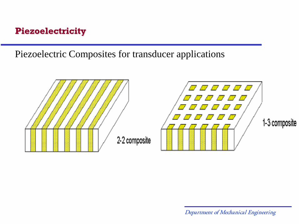
Piezoelectricity
Piezoelectric Composites for transducer applications
Department of Mechanical Engineering
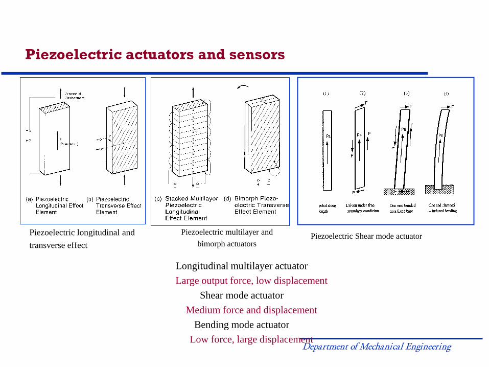
Piezoelectric longitudinal andtransverse effect
Piezoelectric multilayer andbimorph actuators
Piezoelectric Shear mode actuator
Longitudinal multilayer actuatorLarge output force, low displacement
Shear mode actuatorMedium force and displacement
Bending mode actuatorLow force, large displacement
Piezoelectric actuators and sensors
Department of Mechanical Engineering
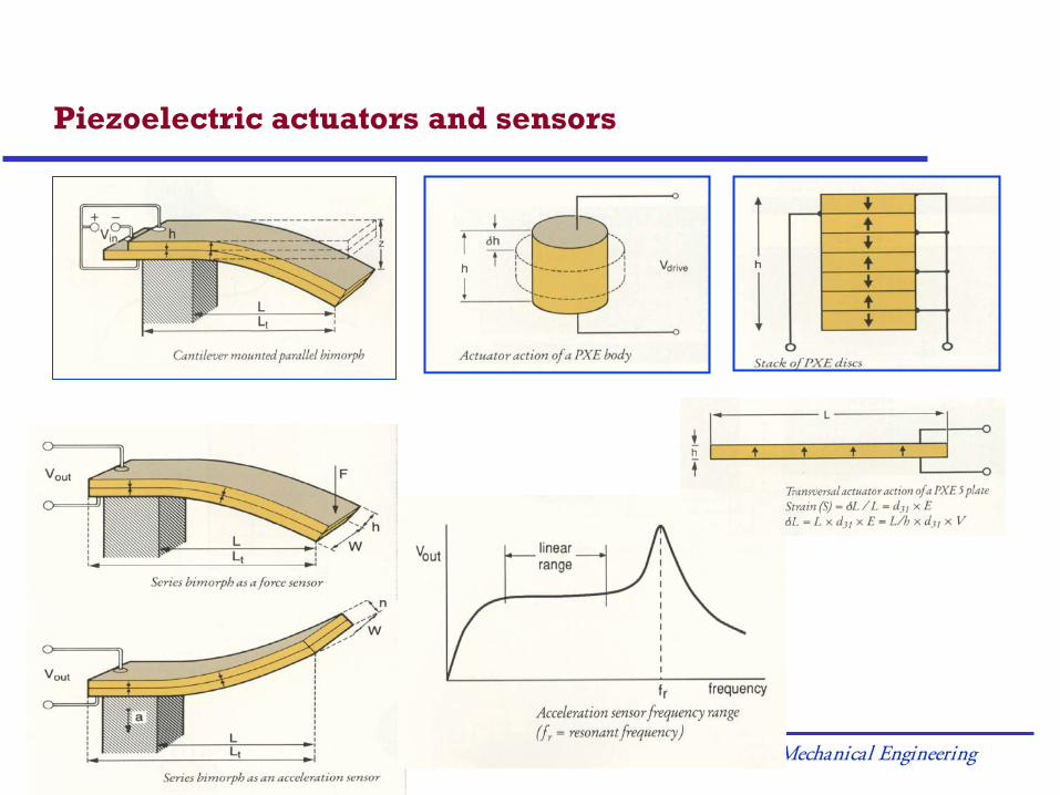
Piezoelectric actuators and sensors
Department of Mechanical Engineering
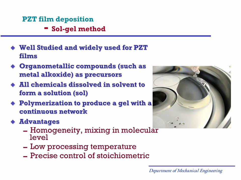
PZT film deposition - Sol-gel method
Well Studied and widely used for PZT films
Organometallic compounds (such as metal alkoxide) as precursors
All chemicals dissolved in solvent to form a solution (sol)
Polymerization to produce a gel with a continuous network
AdvantagesHomogeneity, mixing in molecular
levelLow processing temperaturePrecise control of stoichiometric
Department of Mechanical Engineering
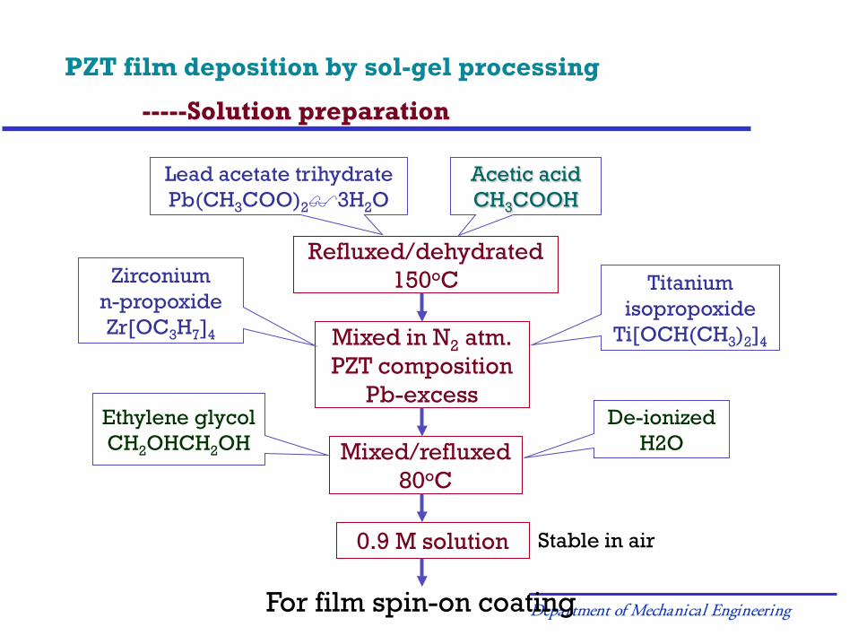
PZT film deposition by sol-gel processing
-----Solution preparation
Refluxed/dehydrated150oC
Mixed in N2 atm.PZT composition
Pb-excess
Titaniumisopropoxide
Ti[OCH(CH3)2]4
Zirconiumn-propoxideZr[OC3H7]4
Mixed/refluxed80oC
De-ionizedH2O
Ethylene glycolCH2OHCH2OH
Lead acetate trihydratePb(CH3COO)23H2O
Acetic acidCH3COOH
0.9 M solution Stable in air
For film spin-on coating
Department of Mechanical Engineering
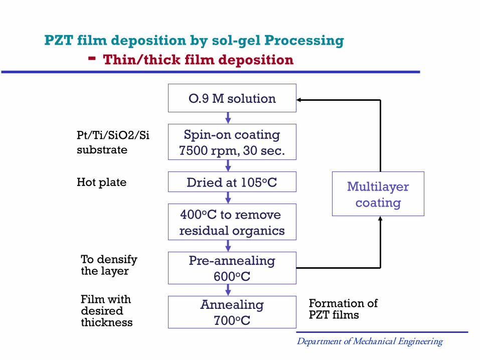
PZT film deposition by sol-gel Processing- Thin/thick film deposition
O.9 M solution
Pre-annealing600oC
400oC to remove residual organics
Hot plate
Spin-on coating7500 rpm, 30 sec.
Pt/Ti/SiO2/Si substrate
Dried at 105oC
To densify the layer
Annealing700oC
Film with desired thickness
Multilayercoating
Formation of PZT films

Department of Mechanical Engineering
P-E Hysteresis Loop
• Sol-gel PZT• 5.0 µm• High P
Department of Mechanical Engineering
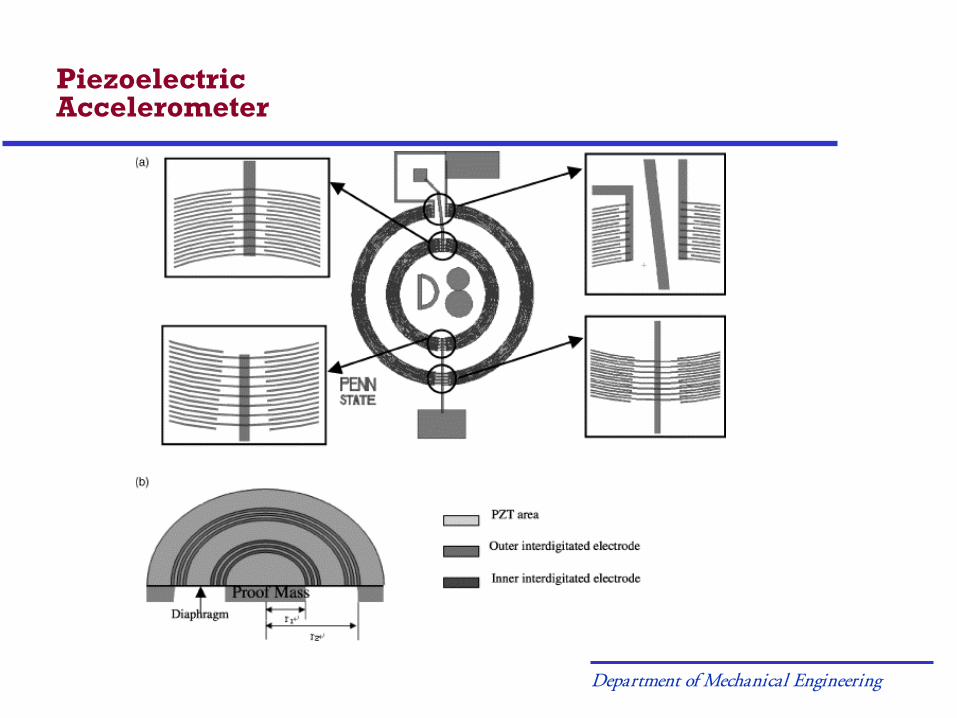
Piezoelectric Accelerometer
Department of Mechanical Engineering
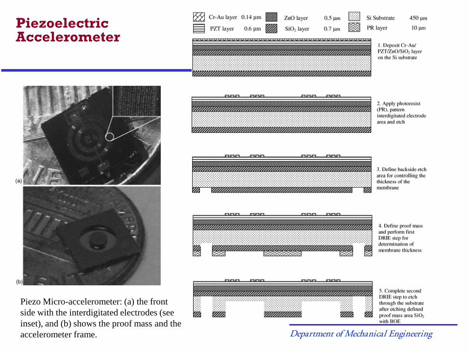
Piezoelectric Accelerometer
Piezo Micro-accelerometer: (a) the front side with the interdigitated electrodes (see inset), and (b) shows the proof mass and the accelerometer frame.
Department of Mechanical Engineering
Piezoelectric Accelerometer
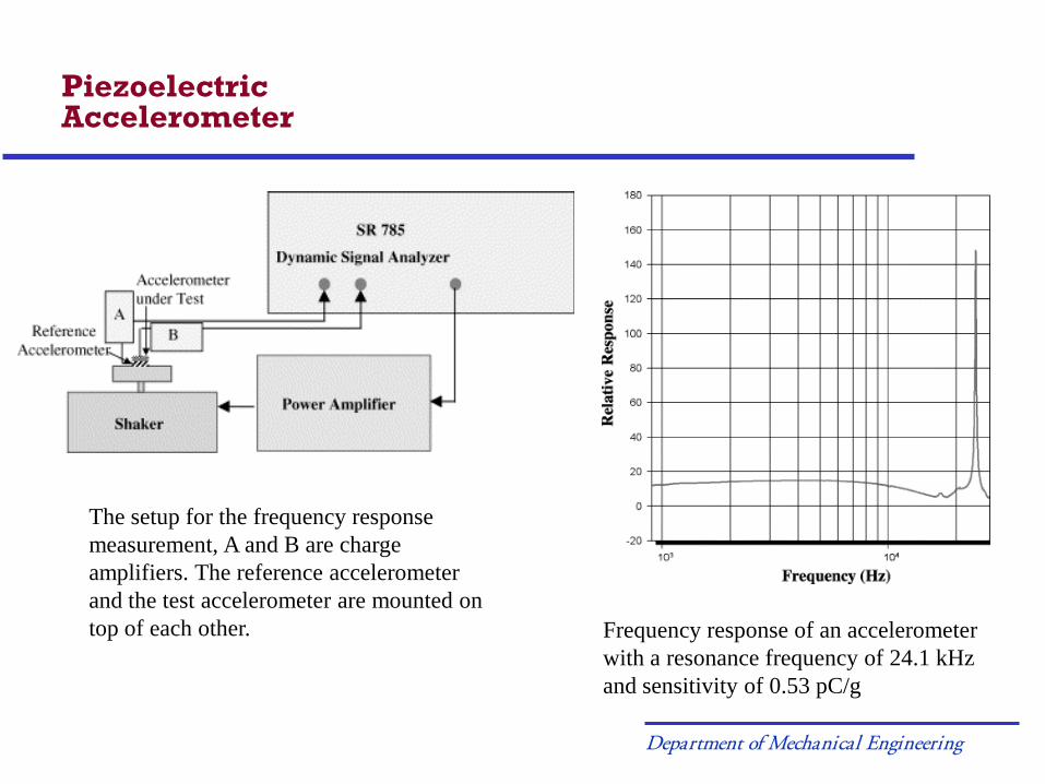
The setup for the frequency response measurement, A and B are charge amplifiers. The reference accelerometer and the test accelerometer are mounted on top of each other. Frequency response of an accelerometer
with a resonance frequency of 24.1 kHz and sensitivity of 0.53 pC/g
Department of Mechanical Engineering
Piezoelectric Accelerometer
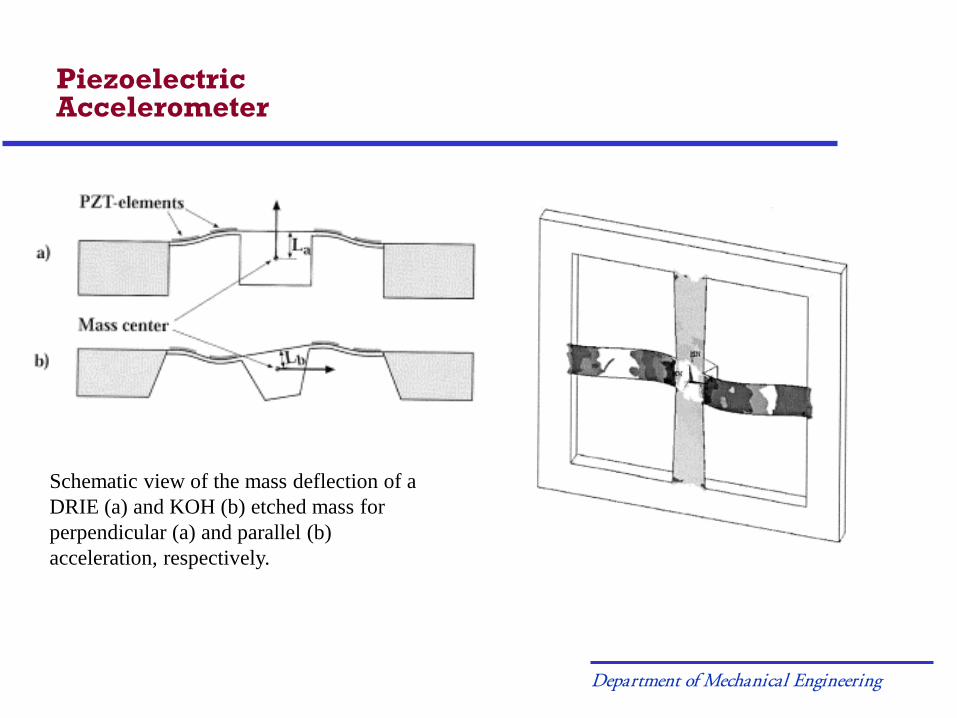
Schematic view of the mass deflection of a DRIE (a) and KOH (b) etched mass for perpendicular (a) and parallel (b) acceleration, respectively.
Department of Mechanical Engineering
Piezoelectric Accelerometer
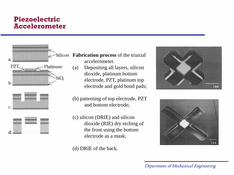
Fabrication process of the triaxial accelerometer.
(a) Depositing all layers, silicon dioxide, platinum bottom electrode, PZT, platinum top electrode and gold bond pads;
(b) patterning of top electrode, PZT and bottom electrode;
(c) silicon (DRIE) and silicon dioxide (RIE) dry etching of the front using the bottom electrode as a mask;
(d) DRIE of the back.
Department of Mechanical Engineering
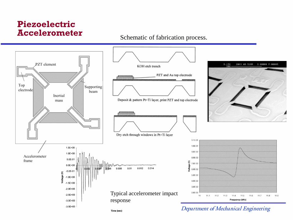
Piezoelectric Accelerometer Schematic of fabrication process.
Typical accelerometer impact response
Department of Mechanical Engineering
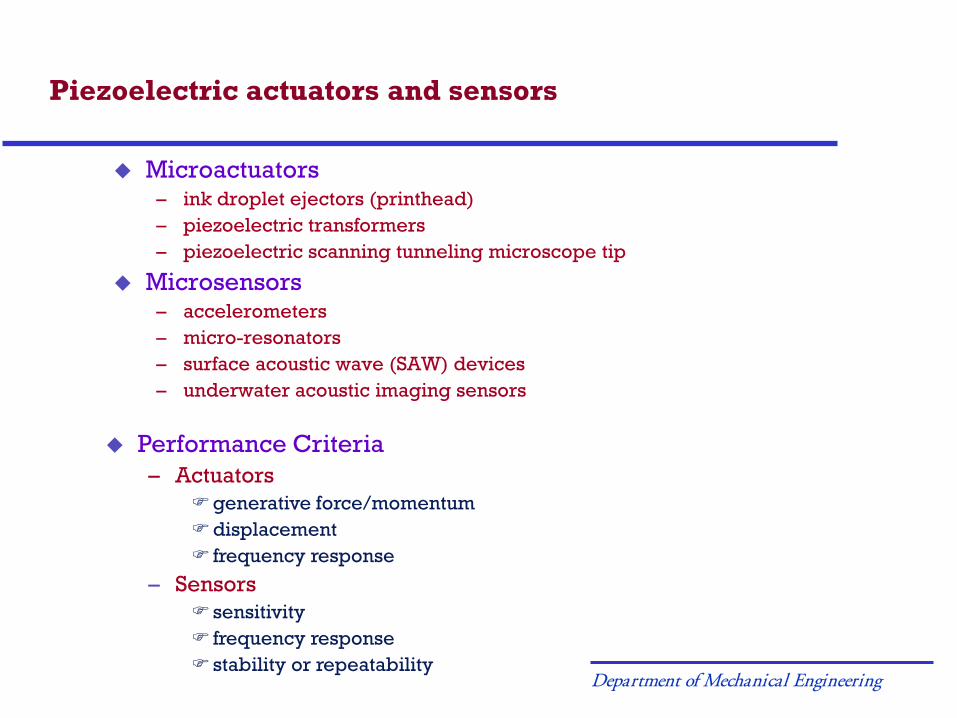
Microactuators– ink droplet ejectors (printhead)– piezoelectric transformers– piezoelectric scanning tunneling microscope tip
Microsensors – accelerometers– micro-resonators– surface acoustic wave (SAW) devices– underwater acoustic imaging sensors
Piezoelectric actuators and sensors
Performance Criteria – Actuators
generative force/momentumdisplacement frequency response
– Sensors sensitivity frequency response stability or repeatability
Department of Mechanical Engineering
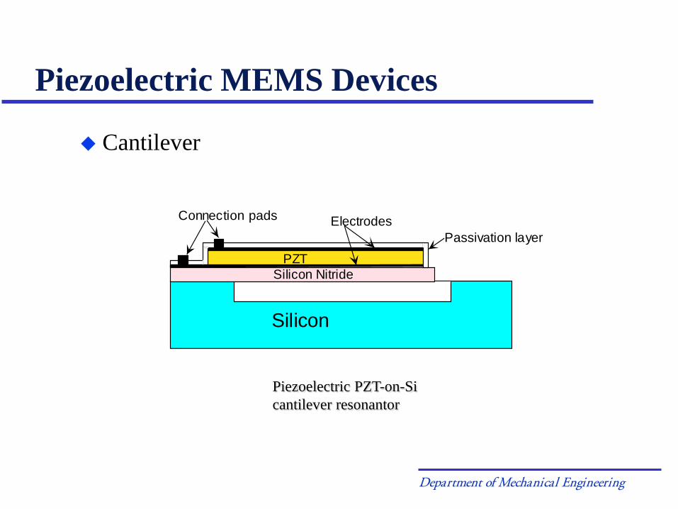
Piezoelectric MEMS Devices
Silicon
Silicon NitridePZT
Passivation layerElectrodesConnection pads
Piezoelectric PZT-on-Si cantilever resonantor
Cantilever
Department of Mechanical Engineering
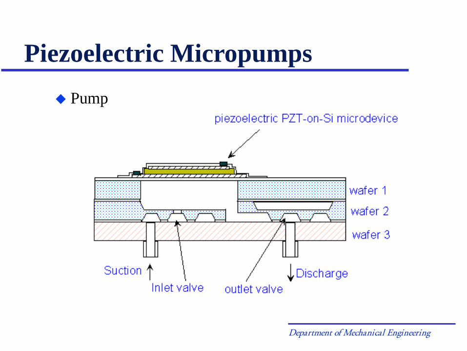
Piezoelectric Micropumps Pump
Department of Mechanical Engineering
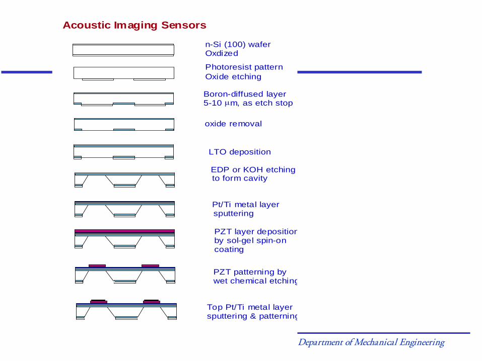
Photoresist patternOxide etching
Boron-diffused layer5-10 m, as etch stopµ
oxide removal
LTO deposition
Pt/Ti metal layersputtering
PZT layer depositionby sol-gel spin-oncoating
EDP or KOH etchingto form cavity
PZT patterning bywet chemical etching
Top Pt/Ti metal layersputtering & patterning
Acoustic Imaging Sensors
n-Si (100) waferOxdized
Department of Mechanical Engineering
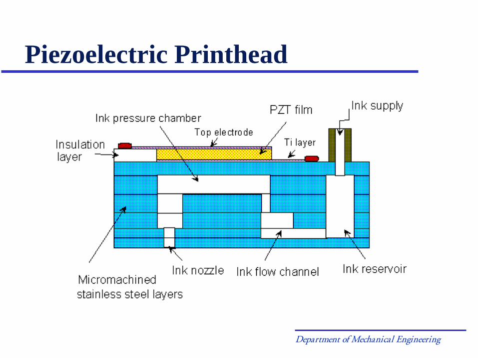
Piezoelectric Printhead
Department of Mechanical Engineering
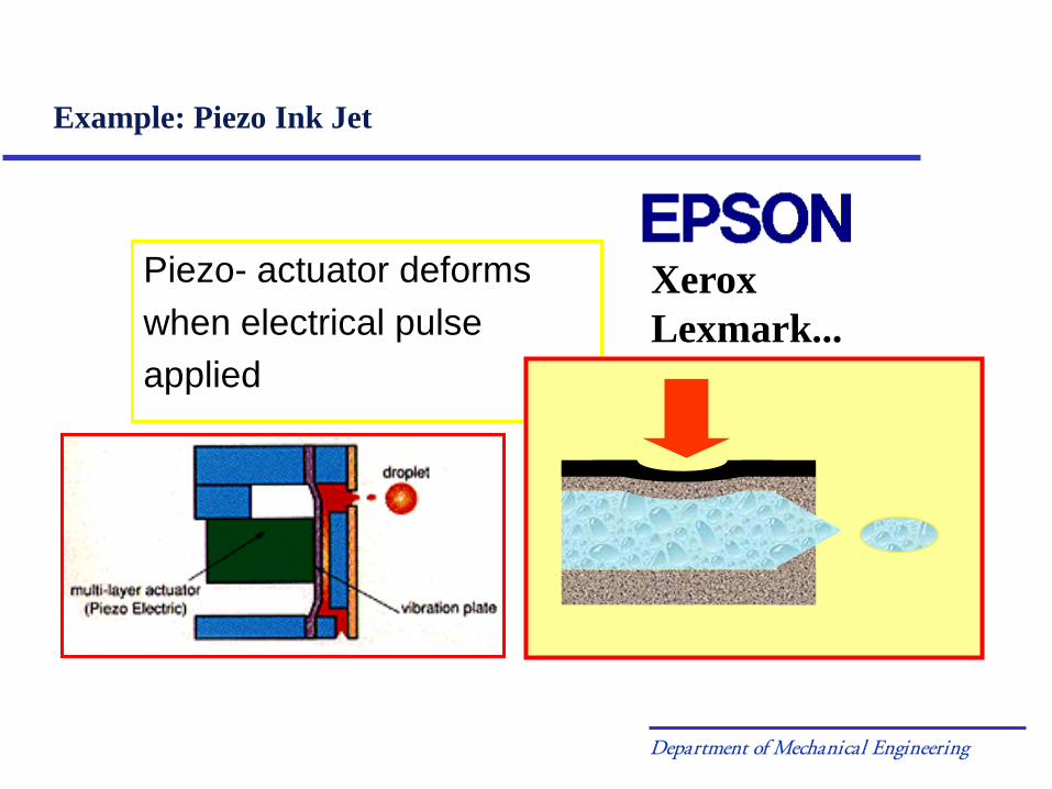
Piezo- actuator deforms when electrical pulseapplied
Example: Piezo Ink Jet
XeroxLexmark...
Department of Mechanical Engineering
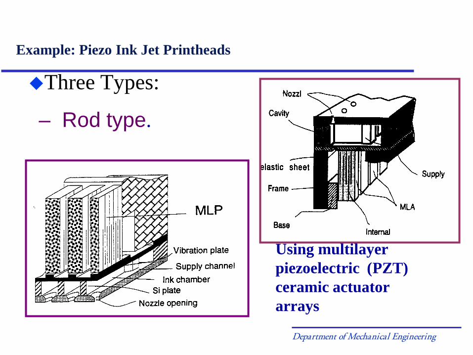
Example: Piezo Ink Jet Printheads
Three Types:
Using multilayer piezoelectric (PZT) ceramic actuator arrays
– Rod type.
Department of Mechanical Engineering
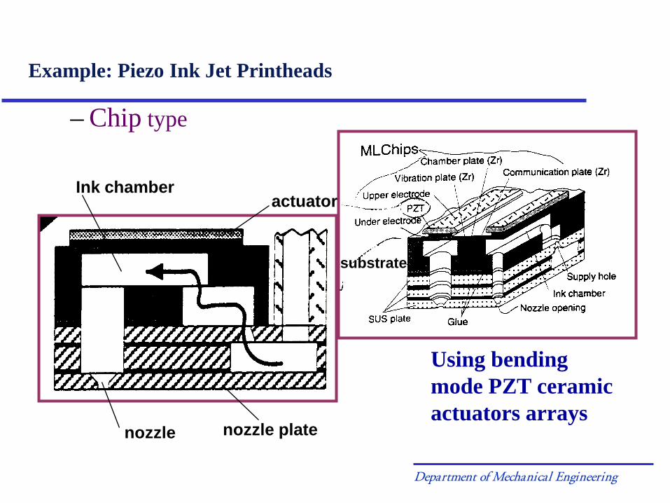
Example: Piezo Ink Jet Printheads
– Chip type
Using bending mode PZT ceramic actuators arrays
substrate
nozzle
actuatorInk chamber
nozzle plate
Department of Mechanical Engineering
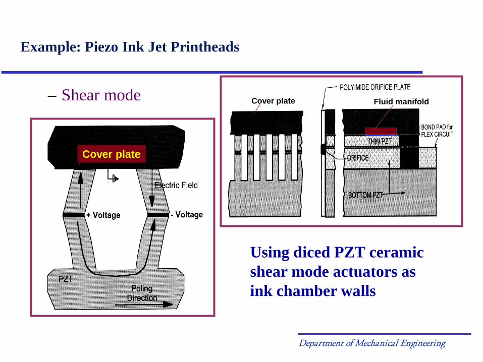
Example: Piezo Ink Jet Printheads
– Shear mode
Using diced PZT ceramic shear mode actuators as ink chamber walls
Cover plate
Cover plate Fluid manifold
Department of Mechanical Engineering
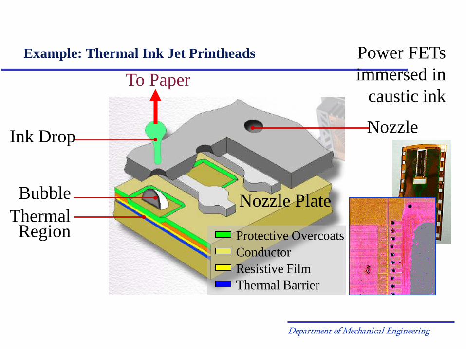
Example: Thermal Ink Jet Printheads Power FETs immersed in
caustic ink
Nozzle Plate
Protective OvercoatsConductorResistive FilmThermal Barrier
Ink Drop
BubbleThermalRegion
To Paper
Nozzle
Department of Mechanical Engineering
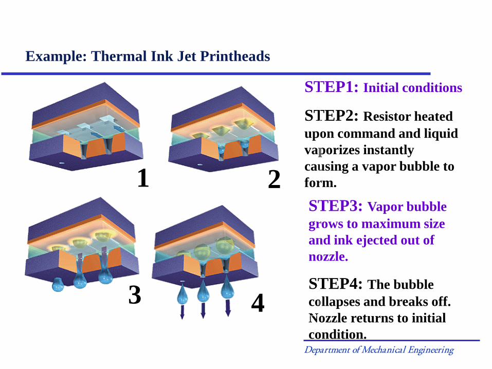
STEP1: Initial conditions
STEP2: Resistor heated upon command and liquid vaporizes instantly causing a vapor bubble to form.
STEP3: Vapor bubble grows to maximum size and ink ejected out of nozzle.
STEP4: The bubble collapses and breaks off. Nozzle returns to initial condition.
1 2
3 4
Example: Thermal Ink Jet Printheads
Department of Mechanical Engineering
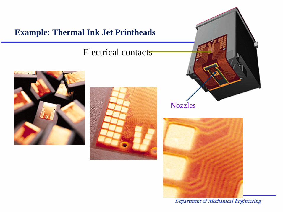
Nozzles
Electrical contacts
Example: Thermal Ink Jet Printheads
Department of Mechanical Engineering
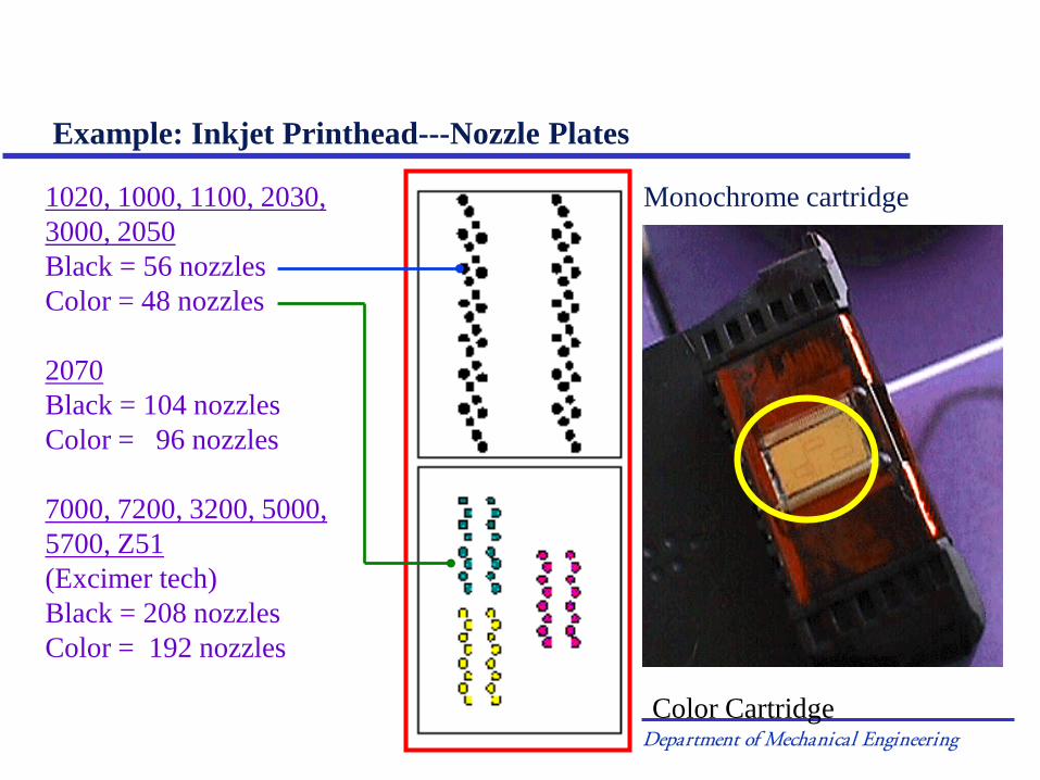
Monochrome cartridge1020, 1000, 1100, 2030, 3000, 2050Black = 56 nozzlesColor = 48 nozzles
2070 Black = 104 nozzlesColor = 96 nozzles
7000, 7200, 3200, 5000, 5700, Z51 (Excimer tech)Black = 208 nozzlesColor = 192 nozzles
Example: Inkjet Printhead---Nozzle Plates
Color Cartridge
Department of Mechanical Engineering
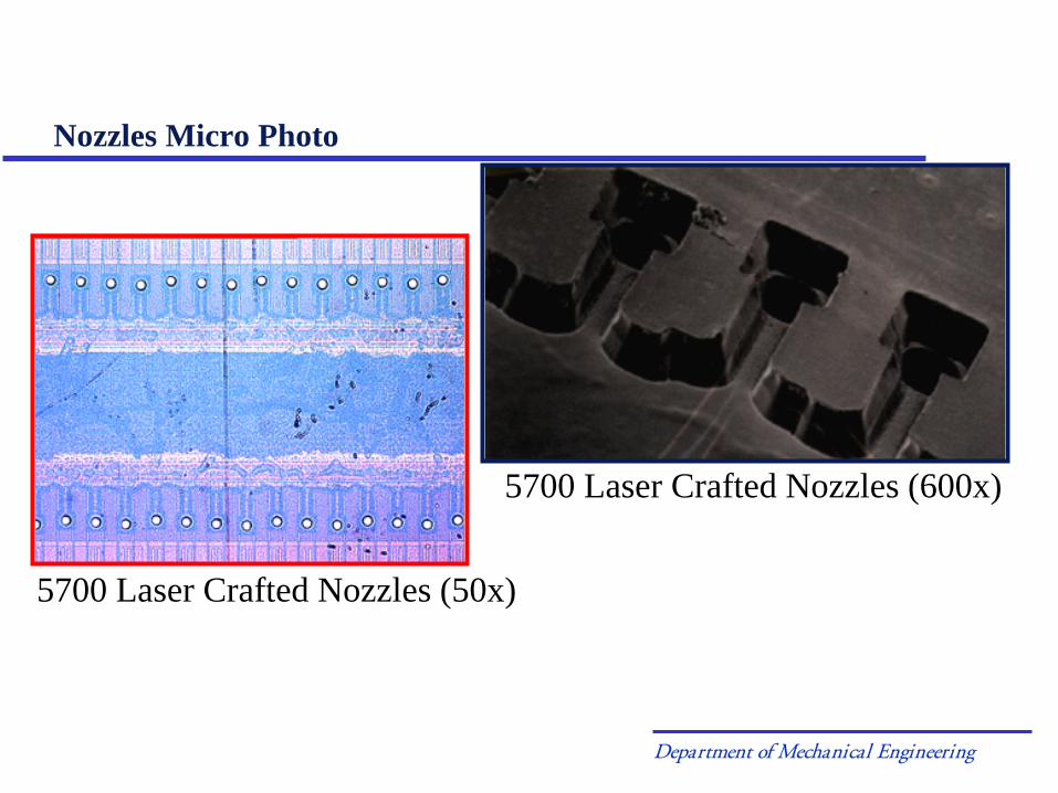
5700 Laser Crafted Nozzles (600x)
5700 Laser Crafted Nozzles (50x)
Nozzles Micro Photo
Department of Mechanical Engineering
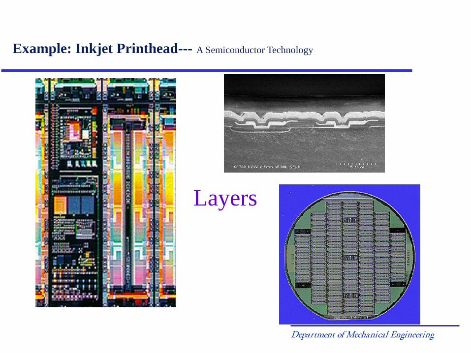
Layers
Example: Inkjet Printhead--- A Semiconductor Technology
Department of Mechanical Engineering
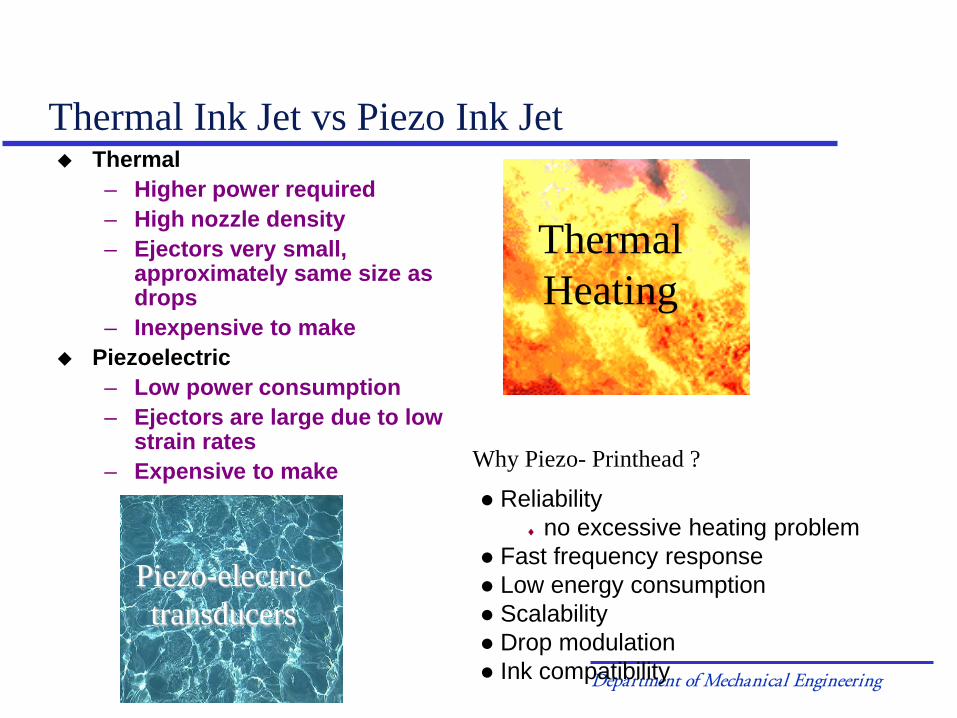
Thermal Ink Jet vs Piezo Ink Jet Thermal
– Higher power required– High nozzle density– Ejectors very small,
approximately same size as drops
– Inexpensive to make Piezoelectric
– Low power consumption– Ejectors are large due to low
strain rates– Expensive to make Why Piezo- Printhead ?
Reliability♦ no excessive heating problem
Fast frequency response Low energy consumption Scalability Drop modulation Ink compatibility
Piezo-electric transducers
Thermal Heating