Embed Size (px)
Citation preview

ECE 6450 - Dr. Alan DoolittleGeorgia Tech
Lecture 7
Lithography and Pattern Transfer
Reading:
Chapter 7

ECE 6450 - Dr. Alan DoolittleGeorgia Tech
Used for Pattern transfer into oxides, metals, semiconductors.
3 types of Photoresists (PR):
1.) Positive: PR pattern is same as mask. On exposure to light, light degrades the polymers (described in more detail later) resulting in the photoresist being more soluble in developers. The PR can be removed in inexpensive solvents such as acetone.
2.) Negative: PR pattern is the inverse of the mask. On exposure to light, light polymerizes the rubbers in the photoresist to strengthen it’s resistance to dissolution in the developer. The resist has to be removed in special stripping chemicals. Theseresists tend to be extremely moisture sensitive.
3.) Combination: Same photoresist can be used for both negative and positive pattern transfer. Can be removed in inexpensive solvents.
Lithography and Photoresists
Mask Pattern
Pattern transferred to
the Photoresist on the wafer
Positive PR
Light
Negative PR
Light

ECE 6450 - Dr. Alan DoolittleGeorgia Tech
Photoresists are used in a process typical of this process: Dehydration Bake, Apply Adhesion Promoter, Apply Resist, Soft bake, Exposure with Mask, Post Exposure Bake, Develop, Optional Processing. For example:
1.) Dehydration in an oven at ~120 degrees C for as long as 30 minutes
2.) Spin coat (verbally explain) adhesion promoter such as hexamethyldisilane (HMDS)
3.) Spin coat resist
4.) Soft bake to partially solidify PR (85-95 degrees C for 1 to 30 minutes depending on the resist)
5.) Expose to few hundred mJoules/cm2 of high energy light
6.) (Optional) Hard bake, removes more solvent (~110-150 C)
7.) Develop: weak regions of PR dissolved
8.) Additional Hard bake or chemical treatment to harden PR for aggressive processes such as Ion implantation or Plasma etching
Lithography and Photoresists
More details at the Gt microelectronics teaching lab web page: http://www.ece.gatech.edu/research/labs/vc/

ECE 6450 - Dr. Alan DoolittleGeorgia Tech
1) 2)
3) 4)
Applying Photoresists and Related Compounds
Wafer is held on chuck via vacuum and slowly spun.
Photoresist is dispensed
Photoresist is stopped and sucked back to prevent dripping.
Wafer is spun faster to achieve the desired thickness and uniformity.

ECE 6450 - Dr. Alan DoolittleGeorgia Tech
1.) Etching Processes: open windows in oxides for diffusion, masks for ion implantation, etching, metal contact to the semiconductor, or interconnect.
2.) Lift off Processes: Metalization (more common in III-V).
Uses of Lithography:
Wafer
Metal, Oxide, etc…
Photoresist
Wafer
Metal, Oxide, etc…
Wafer Wafer
Spin PR LithographyEtch Layer using
PR as Mask Remove PR
Wafer
Photoresist
Wafer Wafer
Metal
Wafer
Metal
Spin PR Lithography Evaporate Metal Lift Off excess metal with PR

ECE 6450 - Dr. Alan DoolittleGeorgia Tech
1.) Resolution: How small of features can you make. (Current production state of the art is ~0.007 um)
2.) Registration: Can you repeatability align one layer to another. (~1/3 of resolution)
3.) Throughput: Can these be done in a cost effective time. 50-1000 wafers an hour (~200-300 is state of the art), down to 1 chip per hour for prototype or military chips.
At this point, CMOS example will be given in class using supplemental lecture 7b:
Issues with Photolithography

ECE 6450 - Dr. Alan DoolittleGeorgia Tech
1.) Contact: Resist is in contact with the mask: 1:1 magnificationAdvantages: Inexpensive equipment ($~50,000-150,000), moderately high resolution (~0.5 um or better but limited by resist thickness- 0.1 um demonstrated)Disadvantages: Contact with the mask degrades the mask (pinholes and scratches are created on the metal-oxide layers of the mask, particles or dirt are directly imaged in the wafer, Wafer bowing or local loss of planarization results in non-uniform resolution due to mask-wafer gap variations, and no magnification
2.) Proximity: Resist is almost, but not in contact with the mask: 1:1 magnificationAdvantages: Inexpensive equipment, low resolution (~1-2 um or slightly better)Disadvantages: Diffraction effects limit accuracy of pattern transfer. Less repeatable than contact methods, no magnification
3.) Projection: Mask image is projected a distance from the mask and de-magnified to a smaller image: 1:4 -1:10 magnificationAdvantages: Can be very high resolution (~0.007 um or slightly better), No mask contact results in almost no mask wear (high production compatible), mask defects or particles on mask are reduced in size on the wafer.Disadvantages: Extremely expensive and complicated equipment, diffraction effects limit accuracy of pattern transfer.
Photolithography Systems

ECE 6450 - Dr. Alan DoolittleGeorgia Tech
1.) Resolution:Resolution is “diffraction limited”. As patterns approach the same order of magnitude as the wavelength of light, one must be concerned with the wavelike nature of light.
222 rgW
Issues with Photolithography
Case 1: Square Mask in the Near Field (Mask close to Wafer)The mask can be placed in close proximity or directly in contact with the wafer (contact or proximity printing). We define this case, known as the near field or Fresnel diffraction limit, by the expression:
DgWW
r
g
W
D
W
W+W
Definitions used for Resolution Equations

ECE 6450 - Dr. Alan DoolittleGeorgia Tech
(Contd…) Square Mask in the Near Field (Mask close to Wafer)
Effect of increasing mask-wafer gap spacing
Assuming:
2Wg
Then the minimum feature size that can be resolved is:
gkW min
where k is a constant, normally close to 1, that depends on the photoresist and the development procedures
Example: For a k=1, and =0.365 (I-line)Wmin g (gap)
2.7 um 20 um
1.9 um 10 um
1.35 um 5 um
0.6 um 1 um
ECE 6450 - Dr. Alan DoolittleGeorgia Tech
Case 2: Square Mask in the Far Field (Mask far away from the wafer) The mask can be placed far away from the wafer (projection printing used in stepping and scanning systems). We define this case, known as the far field or Fraunhofer diffraction limit, by the expression:
d
The intensity on the wafer (areal image) is then as shown.
Resolution, R, (Diameter of the central maximum) is:
dfR 22.1
d = Diameter of focusing opticsf = Focal length of focusing opticsFrom geometry,
d= 2[n(f sin()] where n is the index of refraction (normally 1 for air but now n.1 is used in “immersion” lithography), and is the angle to the edge of the focusing optics
222 rgW
f
How Quickly the side lobes die off determines the printable pitch

ECE 6450 - Dr. Alan DoolittleGeorgia Tech
(cont’d…) Square Mask in the Far Field (Mask far away from the wafer)
NAkW
min
NAnfnf
dfR
61.0
sin61.0
sin222.122.1
Where NA is the numerical aperture of the focusing optics. The Numerical Aperture describes the focusing strength of the projection system:
However, all our derivation is based on a “point source” which is not ever possible, thus, we can generalize using a constant k (normally ~0.75) the result as:
Briefly discuss immersion lithography.
Immersion Lithography
Lens
Wafer
Immersion Lithography

ECE 6450 - Dr. Alan DoolittleGeorgia Tech
Depth of Focus: While increasing the NA will result in smaller patterns, it also effects the depth of focus (range of lengths for which the image is in focus on the wafer).
2NAfocusofDepth
Large NA results in small Depth of Focus Small NA results in large Depth of Focus
Depth of Focus:
Wafer
Metal LineOxide
Variations in surface heights of a processed wafer must be less than the optical Depth of Focus. Thus, for high resolution lithography the surface must be planar (flat).
Wafer
Metal LineOxide
High resolution (small depth of field) lithography can focus on point A or B but not A and B simultaneously
A
B

ECE 6450 - Dr. Alan DoolittleGeorgia Tech
Comparison of Areal Images of the Three types of Photolithography Systems
ECE 6450 - Dr. Alan DoolittleGeorgia Tech
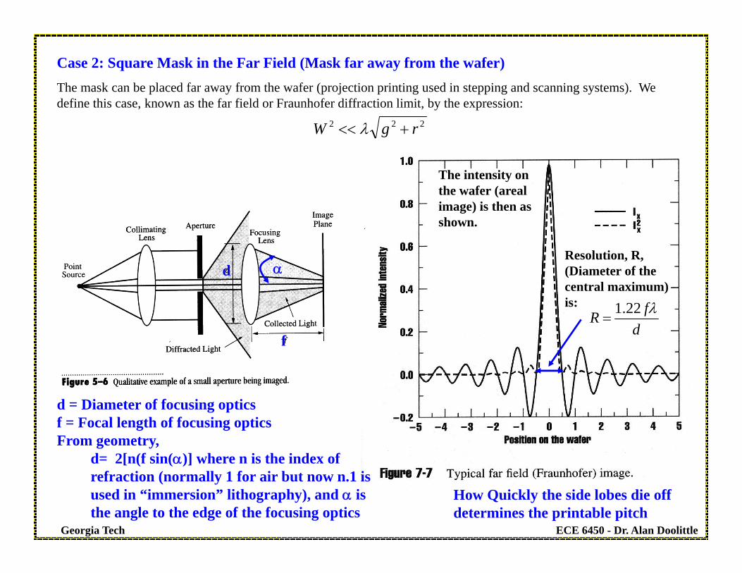
minmax
minmax
IIIIMTF
Consider a diffraction grating instead of a single square aperture, the Fraunhofer limited (far field) intensity pattern (non-normalized intensity in W/cm2) is shown. We can define a measure of the contrast in the areal image (image on the wafer) by the Modulation Transfer Function,
MTF is a measure of an exposure tool’s ability to modulate the intensity of light at the wafer surface and decreases with decreasing diffraction grating period (more destructive interference).
Diffraction Gratings
Light
Diffraction Grating Mask
Intensity Image on
Wafer (Areal image)
Imax
Imin (does not have to =0)

ECE 6450 - Dr. Alan DoolittleGeorgia Tech
The MTF uses the power density (W/cm2 or (J/sec)/cm2). The resist responds to the total amount of energy absorbed. Thus, we need to define the Dose, with units of energy density (mJ/cm2), as the Intensity (or power density) times the exposure time.
•We can also define D100= the minimum dose for which the photoresist will completely dissolve when developed. •We define D0 as the maximum energy density for which the photoresist will not dissolve at all when developed.•Between these values, the photoresist will partially dissolve.
In many cases, we want very high contrast, producing sharp lines. In very few cases, improving step coverage for deposited layers, or even in an image reversal process, one may desire moderately low contrast.
Optical Dose Supplied to PR
Photoresist Pattern after development
Position
PR T
hick
ness

ECE 6450 - Dr. Alan DoolittleGeorgia Tech
Typically mercury (Hg)- Xenon (Xe) vapor bulbs are used as a light source in visible (>420 nm) and ultraviolet (>250-300 nm and <420 nm) lithography equipment. Commonly used molecular transition lines in Hg-Xe bulbs are 436 nm (g-line), 365 (i-line), 290, 280, 265 and 248 nm. All other wavelengths are filtered out.
Lasers are used to increase resolution, and decrease the optical complexity for deep ultraviolet (DUV) lithography systems. Excited dimer (Excimer or Exiplex) pulsed lasers are typically used. These are powerful, extremely expensive to purchase and maintain, optically noisy lasers.
Light Source and Exposure Equipment

ECE 6450 - Dr. Alan DoolittleGeorgia Tech
Steppers and Scanners can have a reduction built in. Thus, a 5X reduction means to produce 0.5 um lines, the mask must have 2.5 um features. Also, dirt or particles on the mask are much smaller on the wafer. Most importantly, defects are consistent from exposure to exposure. Steppers can easily incorporate lasers instead of Hg-vapor bulbs, increasing resolution dramatically.
Where are we today:Pentium II was a 0.25 um technology and was produced exclusively with excimer steppers.Current and future generations of microprocessors will be 0.18, 0.15 and 0.13 um technology.See Predictions from Solid State Technology Table I.
Update: 2017 node is actually 0.007 um
Read sections 7.7, 7.8, 7.9 in your text.
Final Points

ECE 6450 - Dr. Alan DoolittleGeorgia Tech
Updated Status: Lithography
Optical Bulb Stepper
Optical Laser Stepper

ECE 6450 - Dr. Alan DoolittleGeorgia Tech
Updated Status: Lithography

ECE 6450 - Dr. Alan DoolittleGeorgia Tech
Advanced EUV Stepper
Updated Status: Lithography


![2 LASER INTERFERENCE LITHOGRAPHY - uni-halle.de · 2 LASER INTERFERENCE LITHOGRAPHY (LIL) 9 2 LASER INTERFERENCE LITHOGRAPHY (LIL) Laser interference lithography [3~22] (LIL) is a](https://img.pdfslide.us/doc/110x75/5eae180eecc7e273a41a4e88/2-laser-interference-lithography-uni-hallede-2-laser-interference-lithography.jpg)