Embed Size (px)
Citation preview
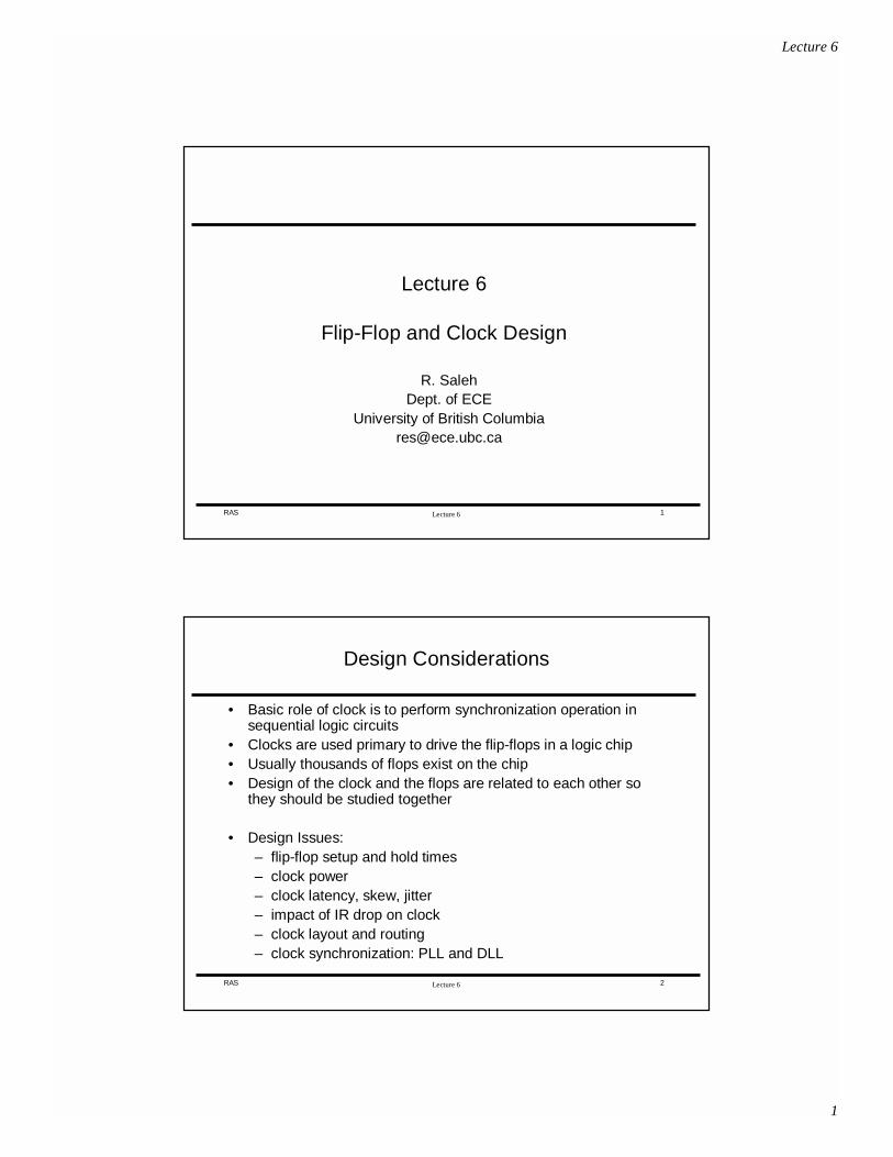
Lecture 6
1
Lecture 6RAS 1
Lecture 6
Flip-Flop and Clock Design
R. SalehDept. of ECE
University of British [email protected]
Lecture 6RAS 2
Design Considerations
• Basic role of clock is to perform synchronization operation in sequential logic circuits
• Clocks are used primary to drive the flip-flops in a logic chip• Usually thousands of flops exist on the chip• Design of the clock and the flops are related to each other so
they should be studied together
• Design Issues:– flip-flop setup and hold times – clock power– clock latency, skew, jitter– impact of IR drop on clock– clock layout and routing– clock synchronization: PLL and DLL
Lecture 6
2
Lecture 6RAS 3
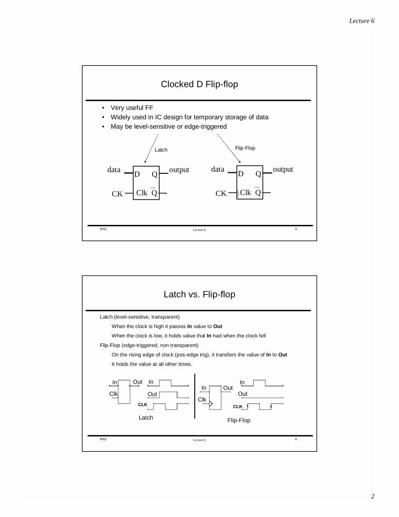
Clocked D Flip-flop
• Very useful FF• Widely used in IC design for temporary storage of data• May be level-sensitive or edge-triggered
CK
D Q
Clk Q
data output
CK
D Q
Clk Q
data output
Latch Flip-Flop
Lecture 6RAS 4
Latch vs. Flip-flop
Latch (level-sensitive, transparent)
When the clock is high it passes In value to Out
When the clock is low, it holds value that In had when the clock fell
Flip-Flop (edge-triggered, non transparent)
On the rising edge of clock (pos-edge trig), it transfers the value of In to Out
It holds the value at all other times.
InIn
OutOut
ClkClk
In
Out Out
In
Latch Flip-Flop
CLK CLK
Lecture 6
3
Lecture 6RAS 5
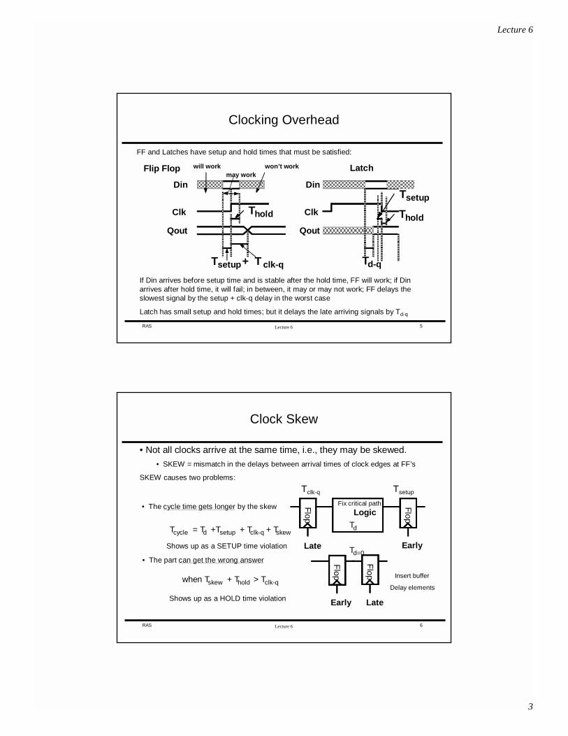
Clocking Overhead
Latch
Din
Clk
Qout
Tsetup+ T clk-q Td-q
Thold
will workFlip Flop won’t workmay work
Thold
Tsetup
FF and Latches have setup and hold times that must be satisfied:
If Din arrives before setup time and is stable after the hold time, FF will work; if Din arrives after hold time, it will fail; in between, it may or may not work; FF delays the slowest signal by the setup + clk-q delay in the worst case
Latch has small setup and hold times; but it delays the late arriving signals by Td-q
Din
Clk
Qout
Lecture 6RAS 6
Clock Skew
Flop
Fl opLogic
Late Early
Tcycle = Td +Tsetup + Tclk-q + Tskew
Flo p
Late
Flop
Early
when Tskew + Thold > Tclk-q
Td
Td=0
• Not all clocks arrive at the same time, i.e., they may be skewed.
• SKEW = mismatch in the delays between arrival times of clock edges at FF’s
SKEW causes two problems:
• The cycle time gets longer by the skew
• The part can get the wrong answer
Tclk-q Tsetup
Shows up as a HOLD time violation
Shows up as a SETUP time violation
Fix critical path
Insert buffer
Delay elements
Lecture 6
4
Lecture 6RAS 7
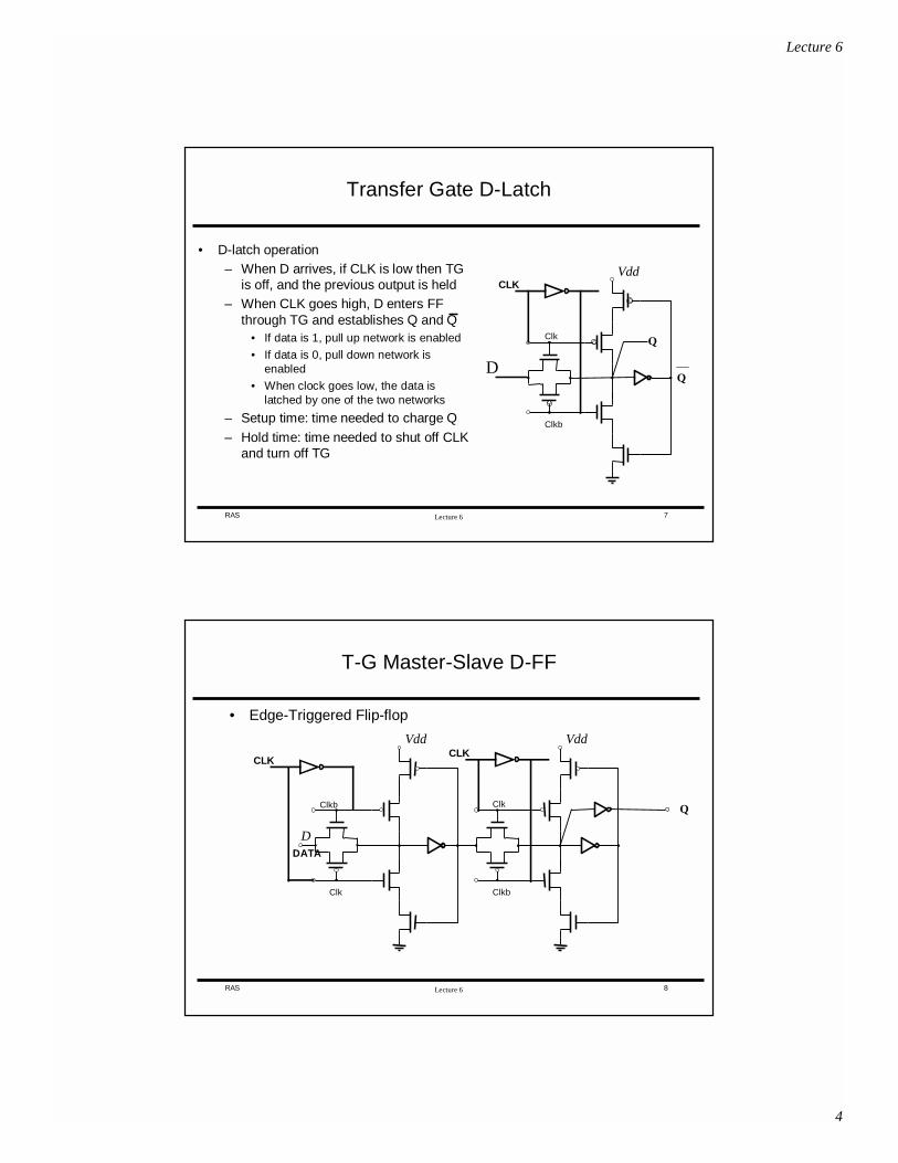
Transfer Gate D-Latch
• D-latch operation– When D arrives, if CLK is low then TG
is off, and the previous output is held– When CLK goes high, D enters FF
through TG and establishes Q and Q• If data is 1, pull up network is enabled
• If data is 0, pull down network is enabled
• When clock goes low, the data is latched by one of the two networks
– Setup time: time needed to charge Q
– Hold time: time needed to shut off CLK and turn off TG
Vdd
Q
CLK
Clkb
Clk
DQ
Lecture 6RAS 8
T-G Master-Slave D-FF
• Edge-Triggered Flip-flop
Vdd Vdd
Q
D
CLK
DATA
CLK
Clkb
Clkb
Clk
Clk
Lecture 6
5
Lecture 6RAS 9
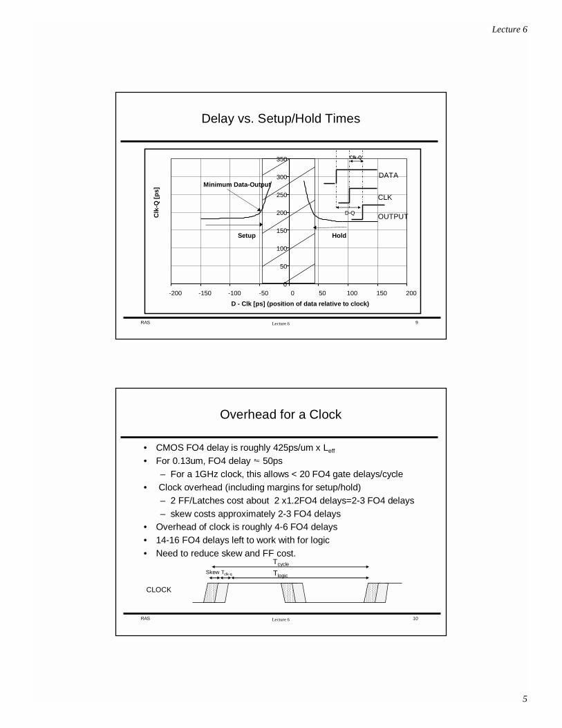
Delay vs. Setup/Hold Times
CLK
DATA
OUTPUT
Clk-Q
0
50
100
150
200
250
300
350
-200 -150 -100 -50 0 50 100 150 200
D - Clk [ps] (position of data relative to clock)
Clk
-Q [
ps]
Setup Hold
Minimum Data-Output
D-Q
Lecture 6RAS 10
Overhead for a Clock
• CMOS FO4 delay is roughly 425ps/um x Leff
• For 0.13um, FO4 delay � 50ps – For a 1GHz clock, this allows < 20 FO4 gate delays/cycle
• Clock overhead (including margins for setup/hold)– 2 FF/Latches cost about 2 x1.2FO4 delays=2-3 FO4 delays– skew costs approximately 2-3 FO4 delays
• Overhead of clock is roughly 4-6 FO4 delays • 14-16 FO4 delays left to work with for logic • Need to reduce skew and FF cost.
CLOCK
Tcycle
Skew Tclk-q Tlogic
Lecture 6
6
Lecture 6RAS 11
Requirements in Flip-Flop Design
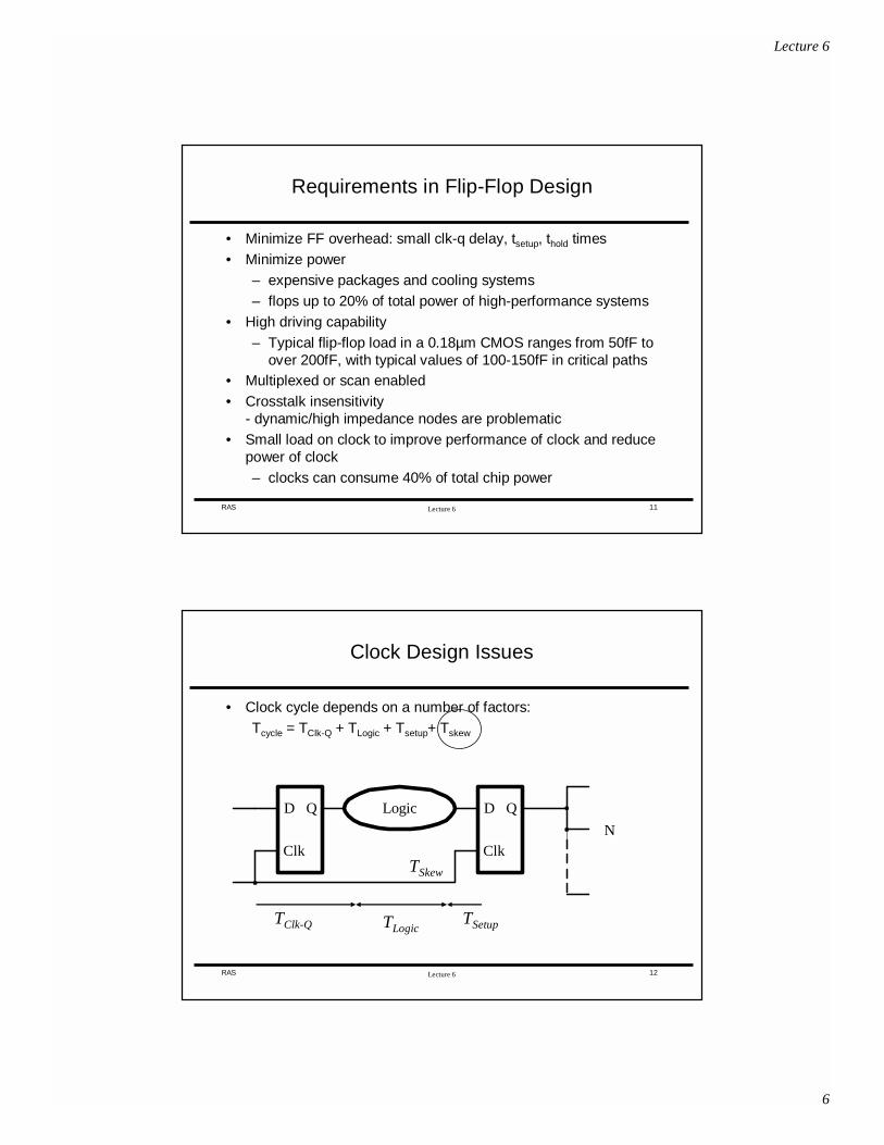
• Minimize FF overhead: small clk-q delay, tsetup, thold times• Minimize power
– expensive packages and cooling systems– flops up to 20% of total power of high-performance systems
• High driving capability – Typical flip-flop load in a 0.18µm CMOS ranges from 50fF to
over 200fF, with typical values of 100-150fF in critical paths• Multiplexed or scan enabled• Crosstalk insensitivity
- dynamic/high impedance nodes are problematic• Small load on clock to improve performance of clock and reduce
power of clock– clocks can consume 40% of total chip power
Lecture 6RAS 12
Clock Design Issues
• Clock cycle depends on a number of factors:Tcycle = TClk-Q + TLogic + Tsetup+ Tskew
D Q
Clk
D Q
Clk
Logic
N
TLogicTClk-Q TSetup
TSkew
Lecture 6
7
Lecture 6RAS 13
Sources of Clock Skew
Main sources:1. Imbalance between different paths from clock source to FF’s
– interconnect length determines RC delays– capacitive coupling effects cause delay variations– buffer sizing– number of loads driven
2. Process variations across die– interconnect and devices have different statistical variations
Secondary Sources:1. IR drop in power supply2. Ldi/dt drop in supply
Lecture 6RAS 14
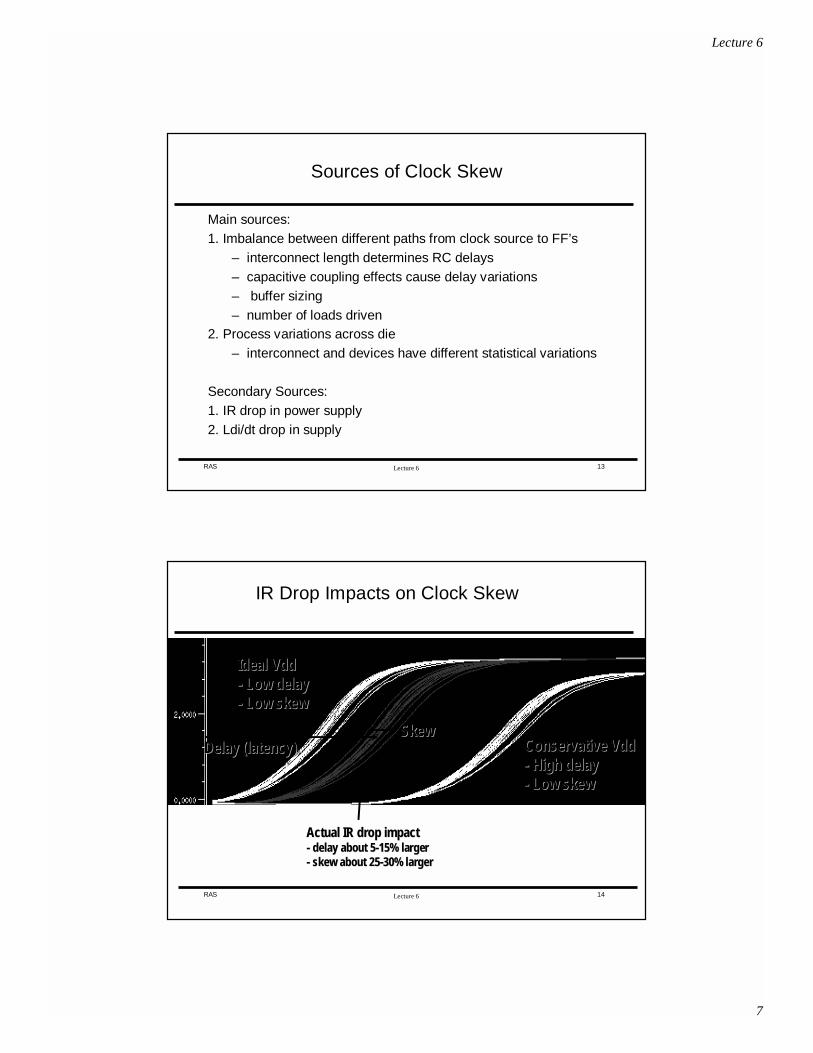
IR Drop Impacts on Clock Skew
Ideal Ideal VddVdd-- Low delayLow delay-- Low skewLow skew
Conservative Conservative VddVdd-- High delayHigh delay-- Low skewLow skew
Actual IR drop impactActual IR drop impact-- delay about 5delay about 5--15% larger15% larger-- skew about 25skew about 25--30% larger30% larger
Delay (latency)Delay (latency)SkewSkew
Lecture 6
8
Lecture 6RAS 15
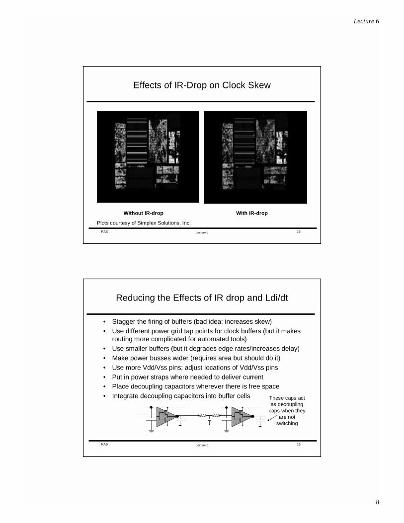
Effects of IR-Drop on Clock Skew
Without IR-drop With IR-drop
Plots courtesy of Simplex Solutions, Inc.
Lecture 6RAS 16
Reducing the Effects of IR drop and Ldi/dt
• Stagger the firing of buffers (bad idea: increases skew)• Use different power grid tap points for clock buffers (but it makes
routing more complicated for automated tools)• Use smaller buffers (but it degrades edge rates/increases delay)• Make power busses wider (requires area but should do it)• Use more Vdd/Vss pins; adjust locations of Vdd/Vss pins• Put in power straps where needed to deliver current• Place decoupling capacitors wherever there is free space• Integrate decoupling capacitors into buffer cells These caps act
as decoupling caps when they
are not switching
Lecture 6
9
Lecture 6RAS 17
Power dissipation in Clocks
• Significant power dissipation can occur in clocks in high-performance designs:
• clock switches on every cycle so P= CV2f (i.e., α=1)• clock capacitance can be ~nF range, say 1nF = 1000pF
• assuming a power supply of 1.8V, CV = 1800pC of charge• if clock switches every 2ns (500MHz), that’s 0.9A• for VDD = 1.8V, P=IV=0.9(1.8)=1.6W in the clock circuit alone
• Much of the power (and the skew) occurs in the final drivers due to the sizing up of buffers to drive the flip-flops
• Key to reducing the power is to examine equation CV2f and reduce the terms wherever possible– VDD is usually given to us; would not want to reduce swing
due to coupling noise, etc.– Look more closely at C and f
Lecture 6RAS 18
Reducing Power in Clocking
• Gated Clocks: – can gate clock signals through AND gate before applying to
flip-flop; this is more of a total chip power savings– all clock trees should have the same type of gating whether
they are used or not, and at the same level - total balance• Reduce overall capacitance (again, shielding vs. spacing)
(a) higher total cap./less area (b) lower cap./ more area
– Tradeoff between the two approaches due to coupling noise– approach (a) is better for inductive noise; (b) is better for
capacitive noise
shield clock shield Signal 1 clock Signal 2
Lecture 6
10
Lecture 6RAS 19
Signal Electromigration
Unidirectional
section
Bidirectional
sections
• Electromigration can occur on certain signal lines• Clocks are prone to EM failures due to large current demand on
every cycle • Since current is bidirectional, we look at RMS current which lead
to Joule heating effects (thermal)• Based on signal activity (frequency of switching)
Irms < 20 mA/um2
Iavg < 10 mA/um2
Lecture 6RAS 20
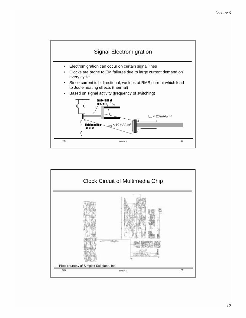
Clock Circuit of Multimedia Chip
Plots courtesy of Simplex Solutions, Inc.
Lecture 6
11
Lecture 6RAS 21
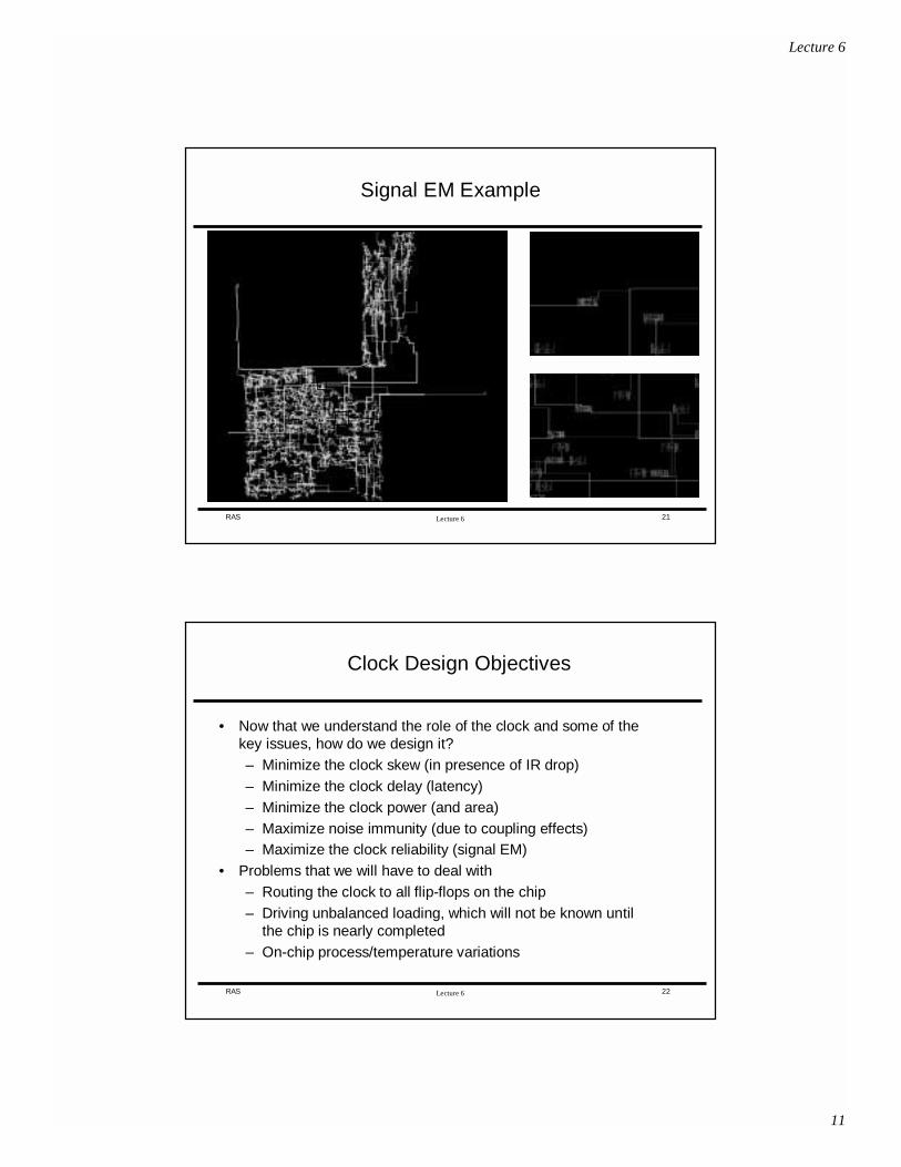
Signal EM Example
Lecture 6RAS 22
Clock Design Objectives
• Now that we understand the role of the clock and some of the key issues, how do we design it?– Minimize the clock skew (in presence of IR drop) – Minimize the clock delay (latency)– Minimize the clock power (and area)– Maximize noise immunity (due to coupling effects)– Maximize the clock reliability (signal EM)
• Problems that we will have to deal with– Routing the clock to all flip-flops on the chip– Driving unbalanced loading, which will not be known until
the chip is nearly completed– On-chip process/temperature variations
Lecture 6
12
Lecture 6RAS 23
Clock Design and Verification
• Many design styles– Low-speed designs: regular signals, symmetric tree– Medium-speed designs: balanced H-tree – High-speed designs
• Balanced buffered H-tree• Grid
• Clock verification is more complex in DSM– RC Interconnect delays– Signal integrity (capacitive coupling, inductance)– IR drop– Signal Electromigration– Clock Jitter
Lecture 6RAS 24
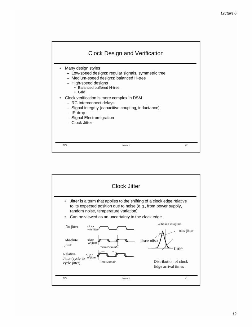
Clock Jitter
clockw/o jitter
clockw/ jitter
Time Domain
Phase Histogram
clockw/ jitter
Time Domain
time
Distribution of clockEdge arrival times
rms jitter
Absolutejitter
RelativeJitter (cycle-to-cycle jitter)
No jitter
phase offset
• Jitter is a term that applies to the shifting of a clock edge relative to its expected position due to noise (e.g., from power supply, random noise, temperature variation)
• Can be viewed as an uncertainty in the clock edge
Lecture 6
13
Lecture 6RAS 25
Secondary clock drivers
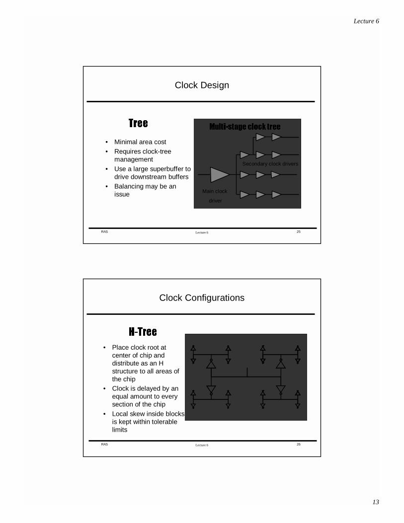
Clock Design
• Minimal area cost• Requires clock-tree
management• Use a large superbuffer to
drive downstream buffers• Balancing may be an
issue
Tree Multi-stage clock tree
Main clock
driver
Lecture 6RAS 26
Clock Configurations
• Place clock root at center of chip and distribute as an H structure to all areas of the chip
• Clock is delayed by an equal amount to every section of the chip
• Local skew inside blocks is kept within tolerable limits
H-Tree
Lecture 6
14
Lecture 6RAS 27
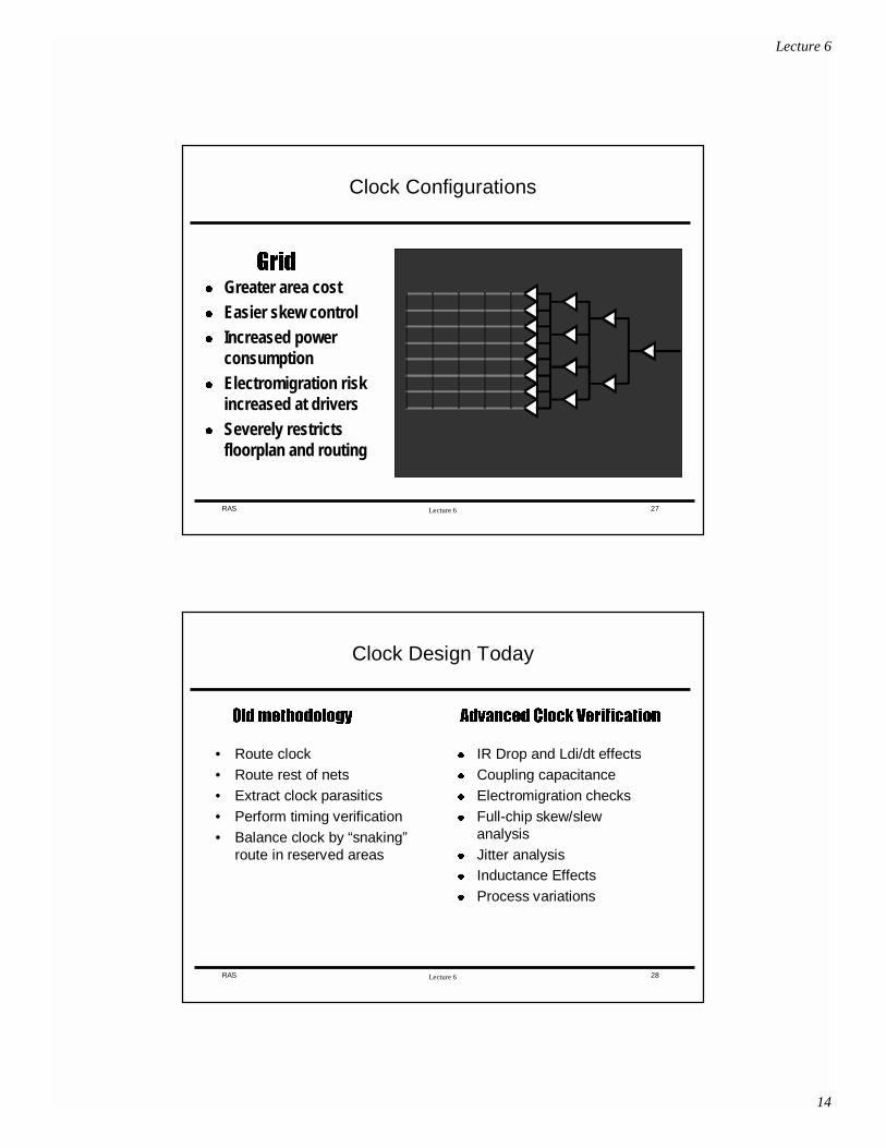
Clock Configurations
� Greater area cost� Easier skew control� Increased power
consumption� Electromigration risk
increased at drivers� Severely restricts
floorplan and routing
Grid
Lecture 6RAS 28
Clock Design Today
• Route clock• Route rest of nets• Extract clock parasitics• Perform timing verification• Balance clock by “snaking”
route in reserved areas
Old methodology Advanced Clock Verification
� IR Drop and Ldi/dt effects� Coupling capacitance� Electromigration checks� Full-chip skew/slew
analysis� Jitter analysis� Inductance Effects� Process variations
Lecture 6
15
Lecture 6RAS 29
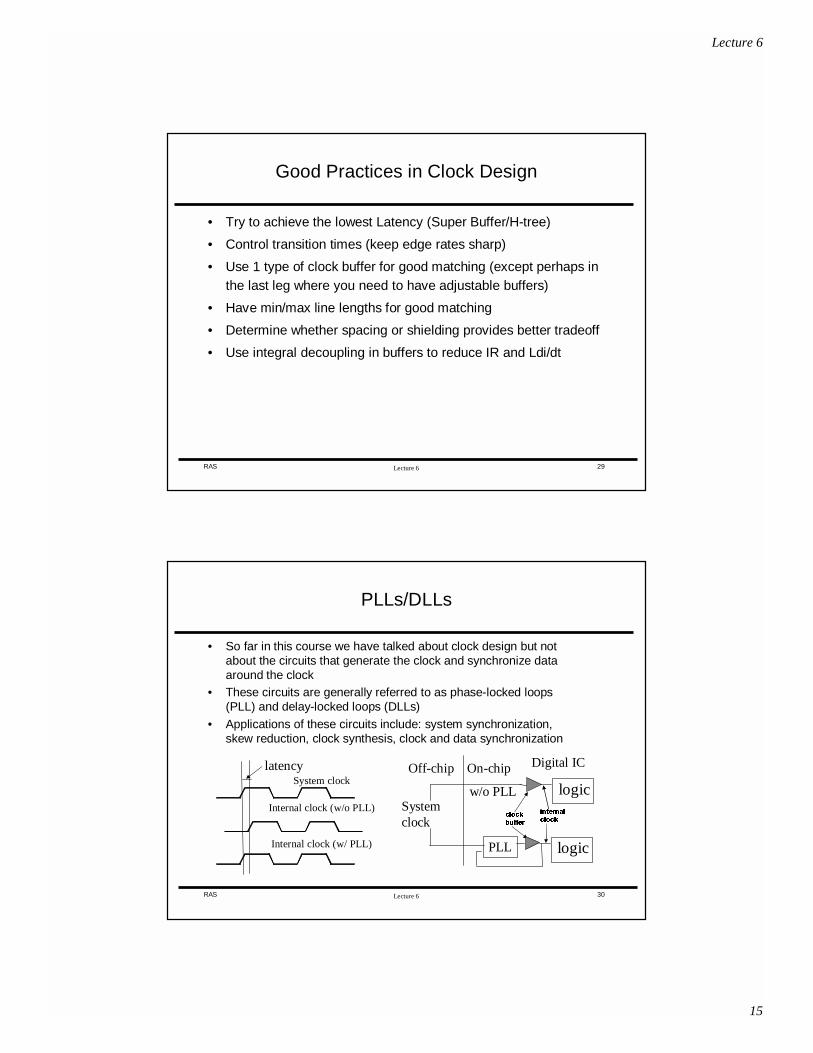
Good Practices in Clock Design
• Try to achieve the lowest Latency (Super Buffer/H-tree)
• Control transition times (keep edge rates sharp)
• Use 1 type of clock buffer for good matching (except perhaps in the last leg where you need to have adjustable buffers)
• Have min/max line lengths for good matching
• Determine whether spacing or shielding provides better tradeoff
• Use integral decoupling in buffers to reduce IR and Ldi/dt
Lecture 6RAS 30
PLLs/DLLs
• So far in this course we have talked about clock design but not about the circuits that generate the clock and synchronize data around the clock
• These circuits are generally referred to as phase-locked loops (PLL) and delay-locked loops (DLLs)
• Applications of these circuits include: system synchronization, skew reduction, clock synthesis, clock and data synchronization
System clock
Internal clock (w/o PLL)
latency
internal
clockclock
buffer
PLL logic
Systemclock
Digital ICOff-chip
logicOn-chip
Internal clock (w/ PLL)
w/o PLL
Lecture 6
16
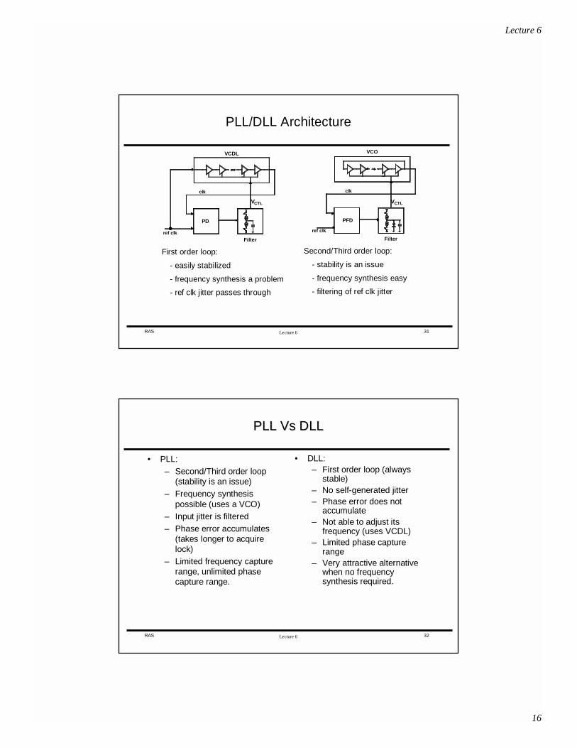
Lecture 6RAS 31
PLL/DLL Architecture
Second/Third order loop:
- stability is an issue
- frequency synthesis easy
- filtering of ref clk jitter
Filter
VCO
ref clk
clk
PFD
First order loop:
- easily stabilized
- frequency synthesis a problem
- ref clk jitter passes through
Filter
VCDL
ref clk
clk
PD
VCTL VCTL
Lecture 6RAS 32
PLL Vs DLLPLL Vs DLL
• PLL:– Second/Third order loop
(stability is an issue)– Frequency synthesis
possible (uses a VCO)– Input jitter is filtered– Phase error accumulates
(takes longer to acquire lock)
– Limited frequency capture range, unlimited phase capture range.
• DLL:– First order loop (always
stable)– No self-generated jitter– Phase error does not
accumulate– Not able to adjust its
frequency (uses VCDL)– Limited phase capture
range– Very attractive alternative
when no frequency synthesis required.