Embed Size (px)
Citation preview

26 April 2021
On-Chip InterconnectAdvanced Digital VLSI Design I
Bar-Ilan University, Course 83-614
Semester B, 2021

April 26, 2021 Adam Teman,
Lecture Overview
2
On-Chip Communication
On-Chip Communication
Connecting with Peripherals
The AMBA Bus
April 26, 2021 Adam Teman,
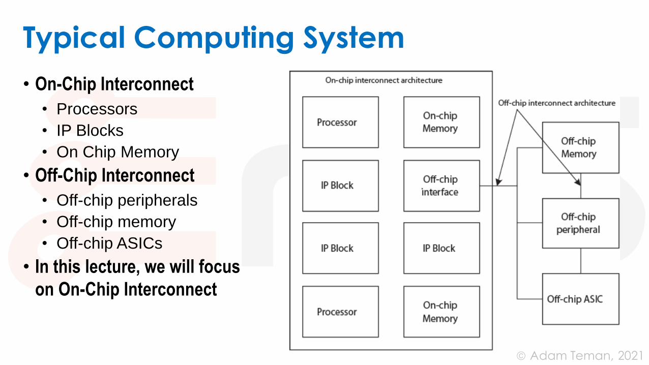
Typical Computing System
• On-Chip Interconnect
• Processors
• IP Blocks
• On Chip Memory
• Off-Chip Interconnect
• Off-chip peripherals
• Off-chip memory
• Off-chip ASICs
• In this lecture, we will focus
on On-Chip Interconnect

April 26, 2021 Adam Teman,
Communication Considerations
System-level issues and specifications for choosing communication architecture:
• Communication Bandwidth• Rate of information transfer (bytes/sec)
• Communication Latency• Time delay between a request and response
• Application dependent, e.g., Video Streaming vs. two-way communication
• Master and Slave• Who can control transactions? What can be controlled?
• Concurrency Requirement• The number of independent simultaneous channels open in parallel.
• Multiple Clock Domains• Different IPs may operate at different frequencies.
5
April 26, 2021 Adam Teman,
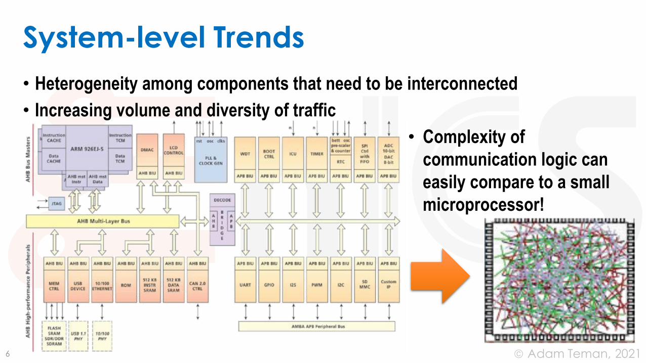
System-level Trends
• Heterogeneity among components that need to be interconnected
• Increasing volume and diversity of traffic
• Complexity of
communication logic can
easily compare to a small
microprocessor!
6

April 26, 2021 Adam Teman,
Interconnect Scaling Trends
• Global wires scale slower than
transistors/gates
• Gates, local wires scale with technology,
global wires do not
• Global on-chip comm to operation
delay changed from 2:1 to 9:1 over
a few technology generations
Source: ITRSSource: Bill Dally, DAC 2009 keynote
April 26, 2021 Adam Teman,
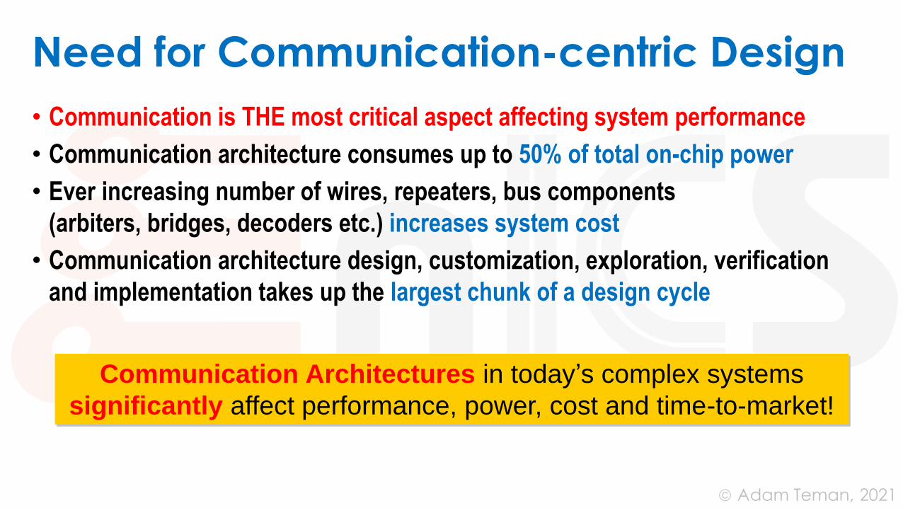
Need for Communication-centric Design
• Communication is THE most critical aspect affecting system performance
• Communication architecture consumes up to 50% of total on-chip power
• Ever increasing number of wires, repeaters, bus components
(arbiters, bridges, decoders etc.) increases system cost
• Communication architecture design, customization, exploration, verification
and implementation takes up the largest chunk of a design cycle
Communication Architectures in today’s complex systems
significantly affect performance, power, cost and time-to-market!

April 26, 2021 Adam Teman,
On-Chip Communication Architecture Design
Three topics to consider when discussing on-chip communication architecture:
• Communication Topology
• How the communication resources are connected
• Simple shared bus, hierarchical bus structures,
rings, mesh, custom bus networks
• Protocols
• How you manage the communication resources
• Static priority, TDMA, round-robin, token passing
• Mapping of System Communications
• Which components connect where?
• e.g., exploit locality, by putting close
components on same bus9
Wingard, Kurosawa,
IEEE CICC, 1998

Connecting with Peripherals
10
On-Chip Communication
Connecting with Peripherals
The AMBA Bus

April 26, 2021 Adam Teman,
Connecting with Memory
• In our discussion of Microprocessors,
we assumed the existence of external memory components:
• In a Princeton Architecture, one homogenous memory space.
• In a Harvard Architecture, separate channels for Instruction and Data Memory
• Before we go into more complex interconnect options, let’s start by looking at
how these tightly-coupled memory blocks are interfaced with the CPU.
Source: Wolf,
Computers as ComponentsHarvard ArchitecturePrinceton Architecture
April 26, 2021 Adam Teman,
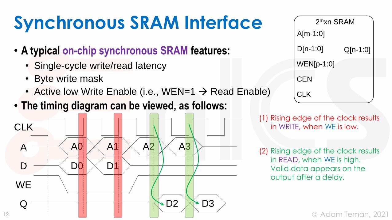
Synchronous SRAM Interface
• A typical on-chip synchronous SRAM features:
• Single-cycle write/read latency
• Byte write mask
• Active low Write Enable (i.e., WEN=1 Read Enable)
• The timing diagram can be viewed, as follows:
12
A[m-1:0]
D[n-1:0]
WEN[p-1:0]
CEN
Q[n-1:0]
2mxn SRAM
CLK
A
CLK
D
WE
Q
A0 A1 A2 A3
D0 D1
D2 D3
(1) Rising edge of the clock results in WRITE, when WE is low.
(2) Rising edge of the clock results
in READ, when WE is high.
Valid data appears on the output after a delay.

April 26, 2021 Adam Teman,
Scaling to a larger network
• The previous SRAM interface is an example of a point-to-point (p2p) link
• P2P links are simple and fast, but not scalable
• Every additional link added requires a full (private) set of signals and control
• Such an approach cannot even accommodate a simple microcontroller,
much less a complex SoC.
• Large amounts of SRAM
• Slower, higher density
memory (DRAM, Flash)
• Peripherals and accelerators
• Therefore, we need a
System Bus.13
Source: Greaves, U. Cambridge

April 26, 2021 Adam Teman,
System Bus
• A collection of signals (wires) to which one or more IP components
(which need to communicate data with each other) are connected.
• In addition to the clock, a synchronous bus consists of:
• An Address Bus
• A Data Bus
• A Control Bus
• In a typical system, the CPU serves
as the bus master (a.k.a. “manager”)
and initiates all transfers.
• Other devices are typically called slaves
(a.k.a. “subordinates”) and they react to transfers initiated by the master.
14
Source: Wolf,
Computers as Components

April 26, 2021 Adam Teman,
Memory Mapping
• Amazingly, the three bus components described above (address, data and
control) can facilitate the majority of required control and data transfer.
• This is thanks to the concept of Memory Mapping
• An n-bit bus supplies 2n unique byte addresses
• With a wide bus (e.g., 32-bits) only a small portion of these
addresses are required for data storage (i.e., memory)
• Therefore, every other device connected to the system is
just treated as a memory address.
• For example, registers of peripherals and accelerators
are given addresses in the system memory map.
• These registers are used to control the devices
(e.g., “start operation” command) as well as to transfer data to and from them.
15
Source: Peckol, Embedded Systems

April 26, 2021 Adam Teman,
Handshaking
• In order to ensure that both devices are ready to communicate over the bus, a
handshaking protocol is required.
• A conceptual handshake protocol utilizes two signals:
• ENQ (enquiry) – from transmitter to receiver
• ACK (acknowledge) – from receiver to transmitter
• The four-cycle handshake process includes:
• Device 1 raises ENQ to initiate transfer
• Device 2 raises ACK, when
ready and transmission can start
• Device 2 lowers ACK to
signal that data was received
• Device 1 lowers ENQ to finish
16
Source: Wolf,
Computers as Components

April 26, 2021 Adam Teman,
Bus Arbitration
• Only one master can control the bus
• Need some way of deciding who is master
• And some way of making sure the right slave answers
• Arbitration
• Decides which master can use the
shared bus if more than one master
requests bus access simultaneously
• Decoding
• Determines the target for any
transfer initiated by a master
• Tells the right slave to put the
response on the bus
17

April 26, 2021 Adam Teman,
Bus Transaction Types
• A transaction on a bus typically involves multiple phases
• Obtaining access to the bus (arbitration phase)
• Sending the address and setting control signals (address phase)
• Sending or receiving the data (data phase)
• Single Transfer
• Simplest transfer mode
• First request for access
to bus from arbiter
• On being granted access,
set address and control signals
• Send data in subsequent cycle
18

April 26, 2021 Adam Teman,
Bus Transaction Types
• Burst Transfer
• Send multiple data items, with only a
single arbitration for the entire transaction
• Master must indicate to arbiter it intends
to perform a burst transfer
• Saves time spent for arbitration
• Pipelined Transfer
• Overlap address and data phases
• Only works if separate address and
data buses are present
• Split Transfer
• Read request and reply are split
19

April 26, 2021 Adam Teman,
Multi-Level Buses
• A microprocessor system often has more than one bus.
• Complexity: High speed buses are more complex (wider and implement
sophisticated protocols), often not required for simple, slower devices.
• Parallelism: Breaking up the bus can provide less contention between devices
that operate independently.
• A bridge connects two buses:
• Acts as a slave on one bus
(e.g., the fast bus)
• Acts as a master on the second
bus (e.g., the slow bus)
• Provides protocol translation
and speed synchronization.
20
Source: Wolf,
Computers as Components

The AMBA Bus
21
On-Chip Communication
Connecting with Peripherals
The AMBA Bus

April 26, 2021 Adam Teman,
What is AMBA?
• The Advanced Microcontroller Bus Architecture (AMBA) is an open-standard,
on-chip interconnect specification for the connection and management of
functional blocks in SoC designs.
• In general:
• AXI = high-speed bus
• AHB = med-speed bus
• APB = low-speed bus
• ACE/CHI =
coherency buses
Source: ARM

April 26, 2021 Adam Teman,
AMBA Multi-Level Approach
• AMBA is designed for multi-level buses
• Commonly use a bridge from a high-speed
bus (e.g., AXI) to a low-speed bus (e.g., APB)
to accommodate low-speed peripherals.
23
PULPino architecture
https://pulp-platform.org/
Source: ARM

April 26, 2021 Adam Teman,
The Advanced Peripheral Bus (APB)
• APB is the simple, low performance bus of the AMBA specification
• APB uses the following signals (Master/Slave):
• PCLK: the bus clock source (rising-edge triggered)
• PRESETn: the bus reset signal (active low)
• PADDR: the APB address bus (can be up to 32-bits wide)
• PSELx: the select line for each slave device
• PENABLE: indicates the 2nd cycle of an APB transfer
• PWRITE: indicates transfer direction (Write=H, Read=L)
• PWDATA: the write data bus (can be up to 32-bits wide)
• PREADY: used to extend a transfer
• PRDATA: the read data bus (can be up to 32-bits wide)
• PSLVERR: indicates a transfer error (OKAY=L, ERROR=H)
24
Source: ARM

April 26, 2021 Adam Teman,
APB Write Transfer
• Setup Phase:
• Address (PADDR), write data (PWDATA), write signal (PWRITE) and select signal
(PSEL) all change after the rising edge of the clock.
• Access Phase:
• The PENABLE signal rises
and the transfer takes place.
• Wait States:
• If the slave lowers PREADYduring the transfer phase,
the transaction is delayed.
25
Each slave has
its own PREADY
Each slave has
its own PSEL
SETUP PHASE
ACCESS PHASE
April 26, 2021 Adam Teman,
APB Read Transfer
• Setup Phase:
• Address (PADDR), write signal (PWRITE) and select signal (PSEL) all change
after the rising edge of the clock.
• Access Phase:
• The PENABLE signal rises
and the PRDATA is driven
by the slave.
• Wait States:
• If the slave lowers PREADYduring the transfer phase,
and only releases the data
when it is raised again.
26
SETUP PHASE
ACCESS PHASE

April 26, 2021 Adam Teman,
APB State Diagram
27
Only remains in the
SETUP state for one clock cycle
Enter ACCESS
state one cycle after SETUP state
Slave pulls PREADYlow to cause WAIT
state
Source: ARM

April 26, 2021 Adam Teman,
Advanced High-Performance Bus (AHB)
• The AMBA AHB bus is the next step up from the APB low-performance bus
• Used for memory interfaces and high-speed peripherals.
• The AMBA AHB achieves higher performance through:
• Burst transfers.
• Single clock-edge operation.
• Non-tristate implementation.
• Wide data bus configurations:
64, 128, 256, 512, and 1024 bits.
28 Master Interface Slave InterfaceSource: ARM

April 26, 2021 Adam Teman,
Advanced High-Performance Bus (AHB)
• Conceptual AHB Block Diagram
29
Decoder selects the correct
slave according to the address.
Multiplexor multiplexes the correct
read data bus and response from
the selected slave.
April 26, 2021 Adam Teman,
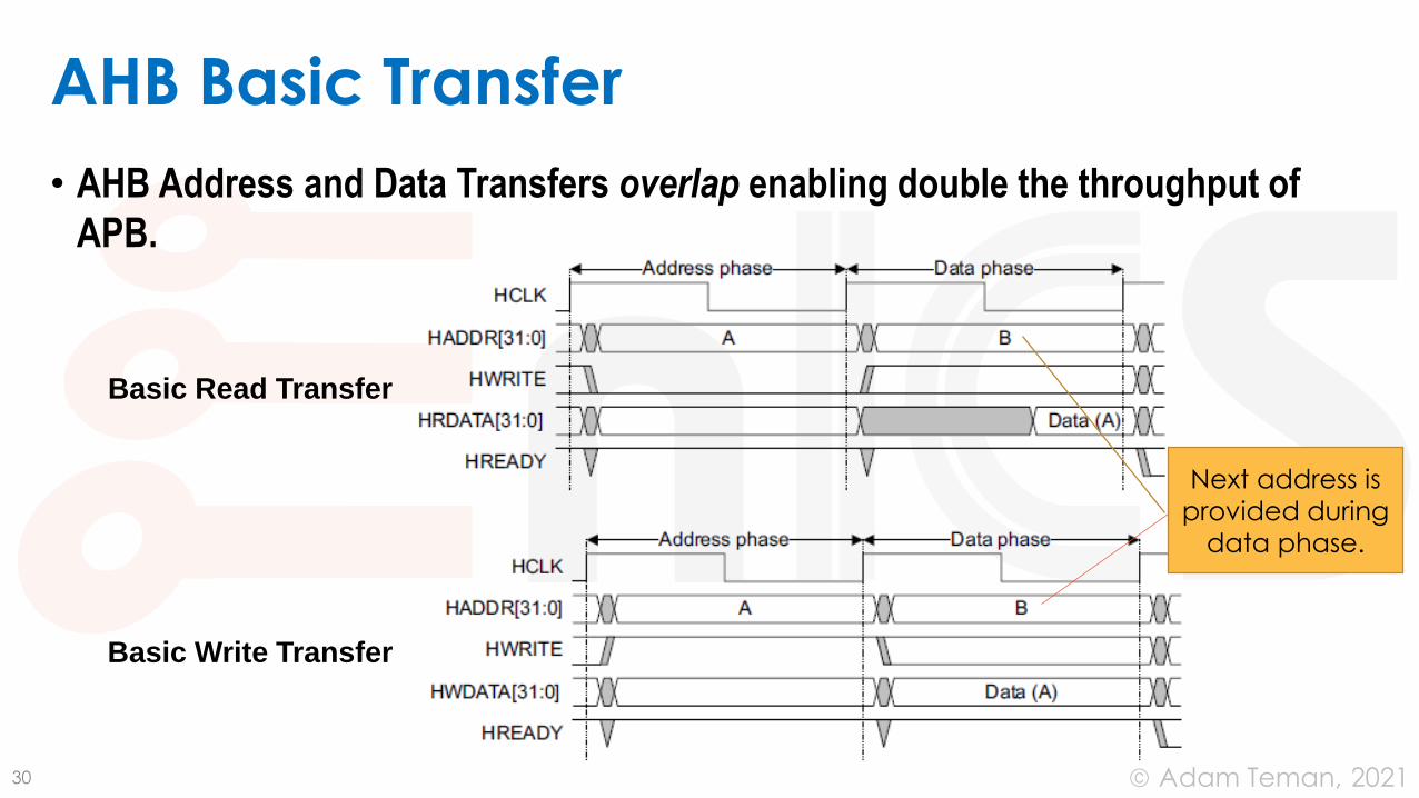
AHB Basic Transfer
• AHB Address and Data Transfers overlap enabling double the throughput of
APB.
30
Basic Read Transfer
Basic Write Transfer
Next address is
provided during
data phase.

April 26, 2021 Adam Teman,
AHB Burst Transfer
• AHB Supports bursts of different lengths
• Master provides one address and the burst length
• Several operations (W/R) are applied to incrementing addresses
• Allows reducing the overhead of the address phase
31
Example:
4-beat Write Burst with
single “wait” state.

April 26, 2021 Adam Teman,
The Advanced eXtensible Interface (AXI)
• AXI is an interface specification that defines the interface of IP blocks,
rather than the interconnect itself.
• AXI supports multiple masters (Managers)
and multiple slaves (Subordinates)
• AXI uses five main channels
(i.e., groups of signals) for communication:
• Write Address (AW)
• Write Data (W)
• Write Response (B)
• Read Address (AR)
• Read Data (R)
• Read response is passed as part of Read Data
32
Source: ARM

April 26, 2021 Adam Teman,
AXI Features
• Independent read and write channels
• Simultaneous reads and writes Improved bandwidth
• Multiple outstanding addresses
• Master can issue new transactions without waiting for previous to complete
• Out-of-order transaction completion
• Transactions have identifiers to support this.
• No strict timing relationship between address and data operations
• Address and data can be arbitrarily separated
• Burst transactions based on start address
• Slave calculates next transfer according to starting address and burst type
• Support for unaligned data transfers
33
April 26, 2021 Adam Teman,
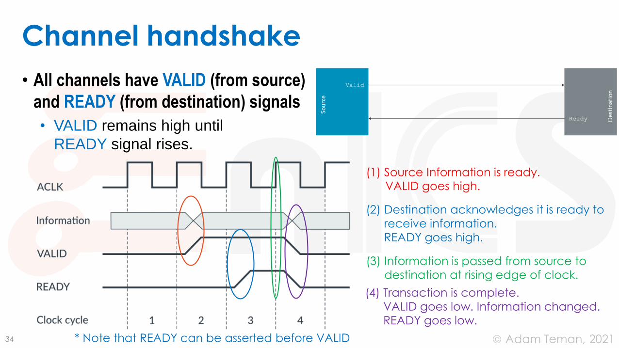
Channel handshake
• All channels have VALID (from source)
and READY (from destination) signals
• VALID remains high until
READY signal rises.
34
(1) Source Information is ready. VALID goes high.
(2) Destination acknowledges it is ready to
receive information. READY goes high.
(4) Transaction is complete.
VALID goes low. Information changed.READY goes low.
(3) Information is passed from source to destination at rising edge of clock.
* Note that READY can be asserted before VALID

April 26, 2021 Adam Teman,
Example: Write Transaction
35
(1) ADDRESS Handshake.
(2) DATA Handshake.
(3) Burst transaction.
WVALID remains high.
(4) WVALID falls.
Pause in transaction
(6) RESPONSE
handshake.
Note that SLAVE is source.
(5) WLAST indicates final data.

April 26, 2021 Adam Teman,
Transaction Ordering
• AXI Supports Interleaved/
Out-of-Order Transactions
• Example of a simple
transaction
• Example of a more
complex transaction
36Source: ARM

April 26, 2021 Adam Teman,
References
• Anand Raghunathan, ECE 695R: System-on-Chip Design
• https://nanohub.org/courses/ECE695R/o1a
• Lectures 1.7, 4.1, 4.2
• Pasricha, Dutt, “On-Chip Communication Architectures”, 2008
• Flynn, Luk “Computer System Design: System-on-Chip”, 2011
• University of Texas, EE319K Introduction to Embedded Systems
• Circuits Basics “BASICS OF UART COMMUNICATION
• ARM AMBA Bus specifications
• AXI Protocol Overview,
https://developer.arm.com/documentation/102202/0200/AXI-protocol-overview
37