Embed Size (px)
Citation preview

Assignment 3 due May 13
Chapter 2Appendix B
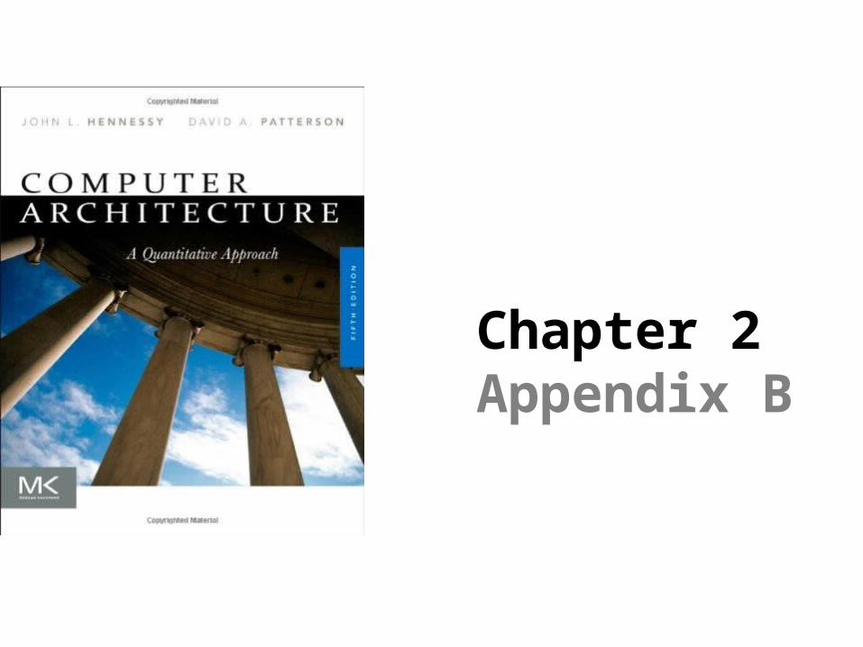
Memory Hierarchy
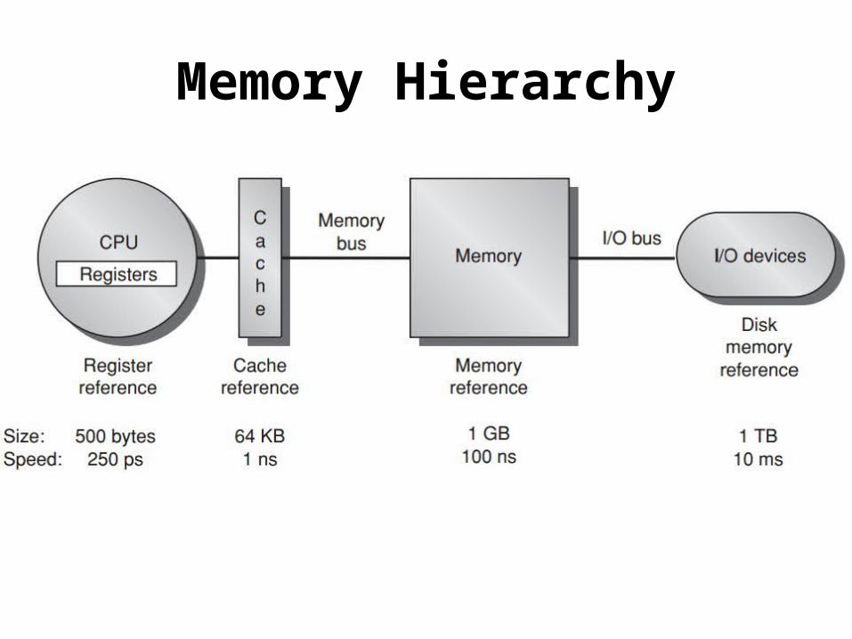
Virtual Memory
Larger memory for more processes
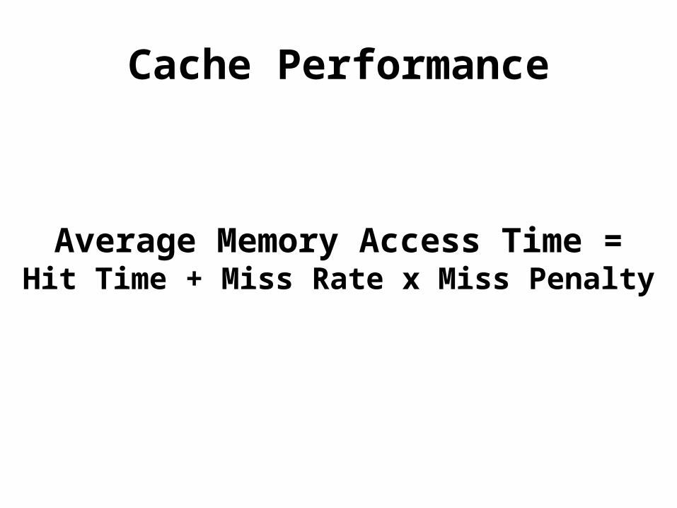
Cache Performance
Average Memory Access Time =Hit Time + Miss Rate x Miss Penalty
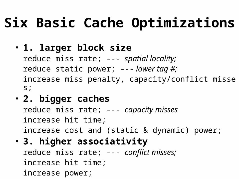
Six Basic Cache Optimizations
• 1. larger block size reduce miss rate; --- spatial locality;reduce static power; --- lower tag #;increase miss penalty, capacity/conflict misses;
• 2. bigger cachesreduce miss rate; --- capacity missesincrease hit time;increase cost and (static & dynamic) power;
• 3. higher associativity reduce miss rate; --- conflict misses;increase hit time;increase power;
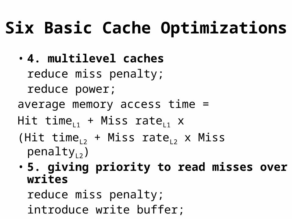
Six Basic Cache Optimizations
• 4. multilevel cachesreduce miss penalty;reduce power;
average memory access time =Hit timeL1 + Miss rateL1 x
(Hit timeL2 + Miss rateL2 x Miss penaltyL2)• 5. giving priority to read misses
over writesreduce miss penalty;introduce write buffer;
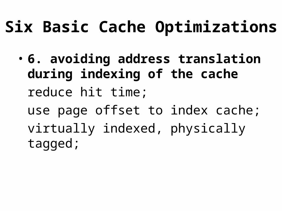
Six Basic Cache Optimizations
• 6. avoiding address translation during indexing of the cachereduce hit time;use page offset to index cache;virtually indexed, physically tagged;
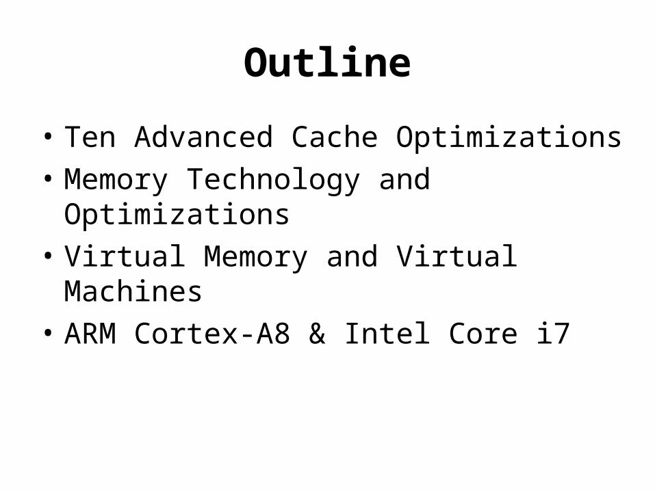
Outline
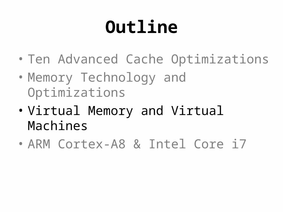
• Ten Advanced Cache Optimizations• Memory Technology and Optimizations• Virtual Memory and Virtual Machines• ARM Cortex-A8 & Intel Core i7
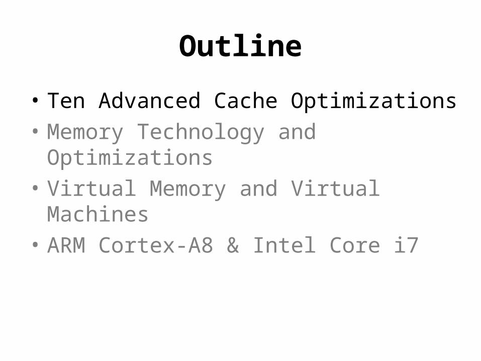
Outline
• Ten Advanced Cache Optimizations• Memory Technology and Optimizations• Virtual Memory and Virtual Machines• ARM Cortex-A8 & Intel Core i7
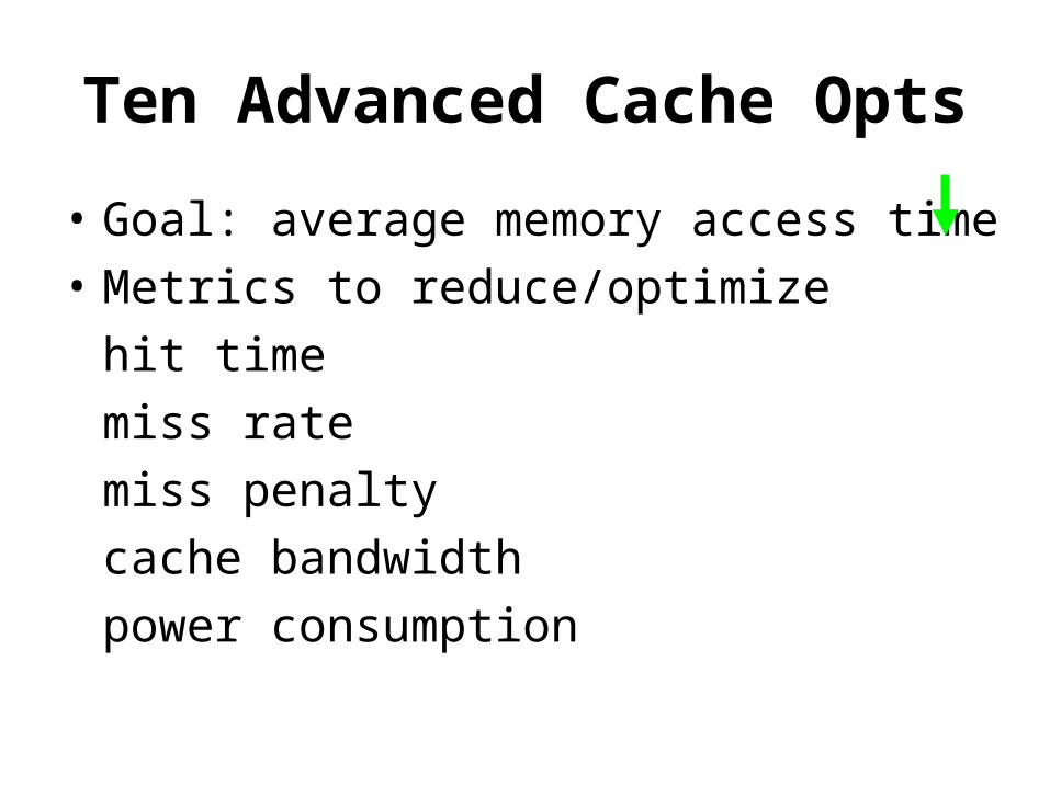
Ten Advanced Cache Opts
• Goal: average memory access time• Metrics to reduce/optimize
hit timemiss ratemiss penaltycache bandwidthpower consumption
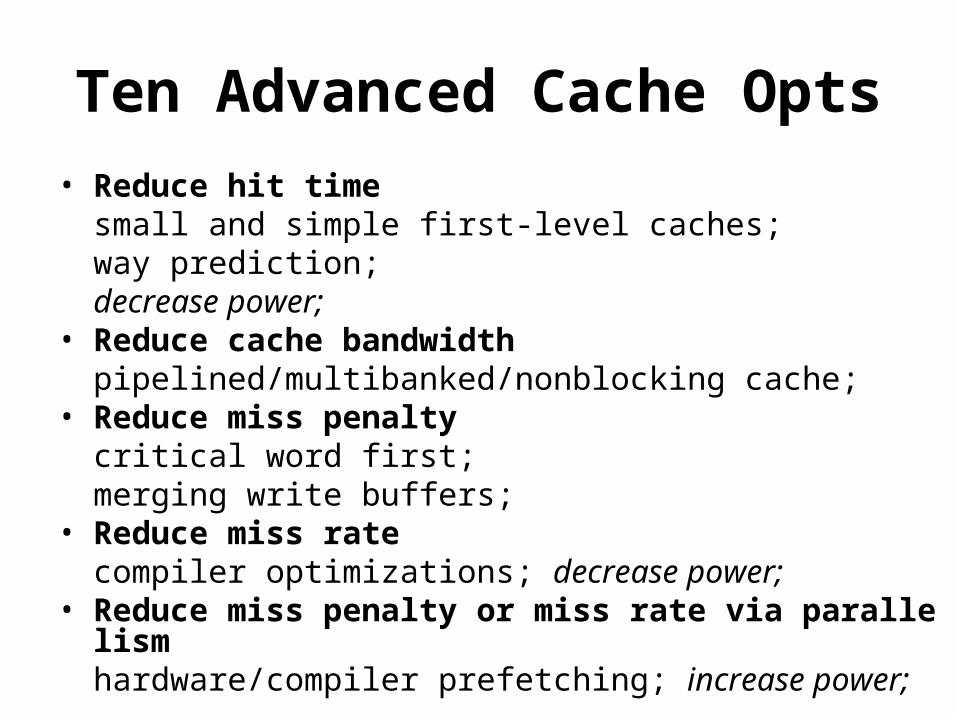
Ten Advanced Cache Opts• Reduce hit time
small and simple first-level caches;way prediction;decrease power;
• Reduce cache bandwidthpipelined/multibanked/nonblocking cache;
• Reduce miss penaltycritical word first;merging write buffers;
• Reduce miss ratecompiler optimizations; decrease power;
• Reduce miss penalty or miss rate via parallelismhardware/compiler prefetching; increase power;
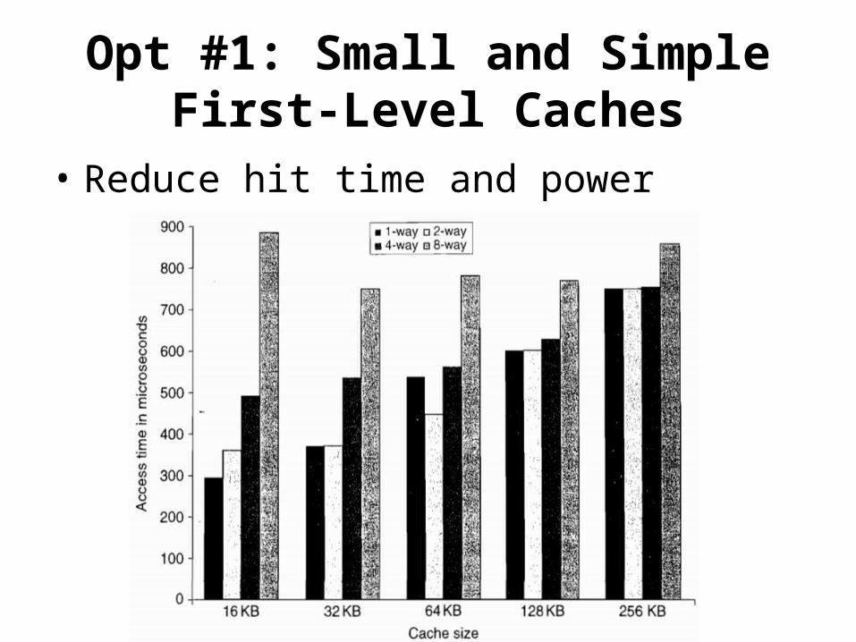
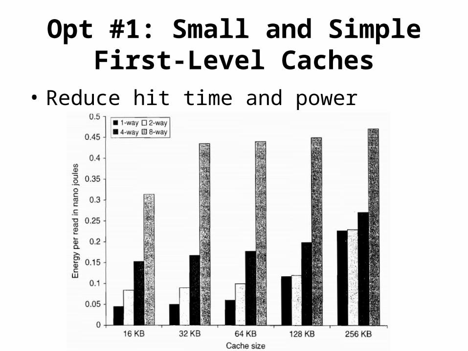
Opt #1: Small and Simple First-Level Caches
• Reduce hit time and power
Opt #1: Small and Simple First-Level Caches
• Reduce hit time and power
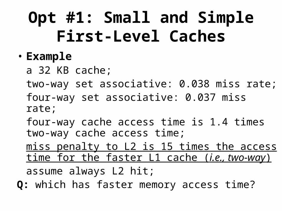
Opt #1: Small and Simple First-Level Caches
• Examplea 32 KB cache;two-way set associative: 0.038 miss rate;four-way set associative: 0.037 miss rate;four-way cache access time is 1.4 times two-way cache access time;miss penalty to L2 is 15 times the access time for the faster L1 cache (i.e., two-way)assume always L2 hit;
Q: which has faster memory access time?
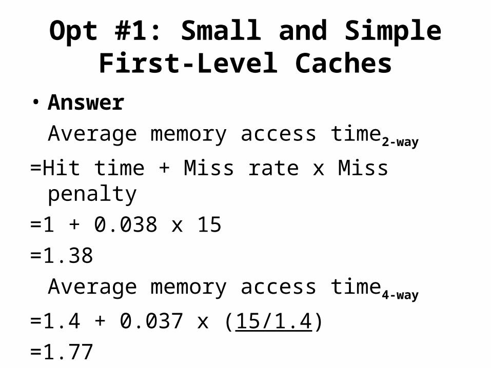
Opt #1: Small and Simple First-Level Caches
• AnswerAverage memory access time2-way
=Hit time + Miss rate x Miss penalty=1 + 0.038 x 15=1.38
Average memory access time4-way
=1.4 + 0.037 x (15/1.4)=1.77
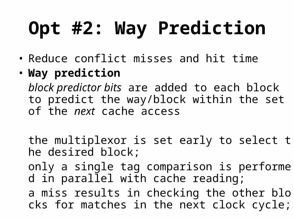
Opt #2: Way Prediction
• Reduce conflict misses and hit time• Way prediction
block predictor bits are added to each block to predict the way/block within the set of the next cache access
the multiplexor is set early to select the desired block;only a single tag comparison is performed in parallel with cache reading;a miss results in checking the other blocks for matches in the next clock cycle;
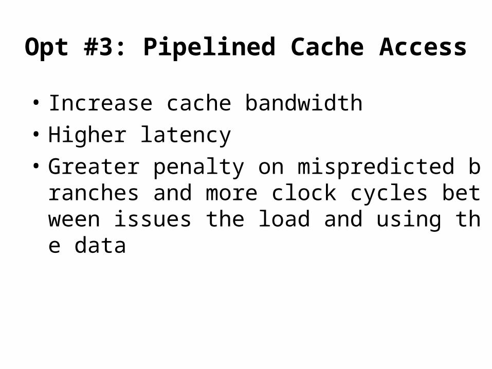
Opt #3: Pipelined Cache Access
• Increase cache bandwidth• Higher latency• Greater penalty on mispredicted branches
and more clock cycles between issues the load and using the data

Opt #4: Nonblocking Caches• Increase cache bandwidth• Nonblocking/lockup-free cache
allows data cache to continue to supply cache hits during a miss;
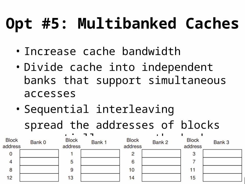
Opt #5: Multibanked Caches• Increase cache bandwidth• Divide cache into independent banks
that support simultaneous accesses• Sequential interleaving
spread the addresses of blocks sequentially across the banks
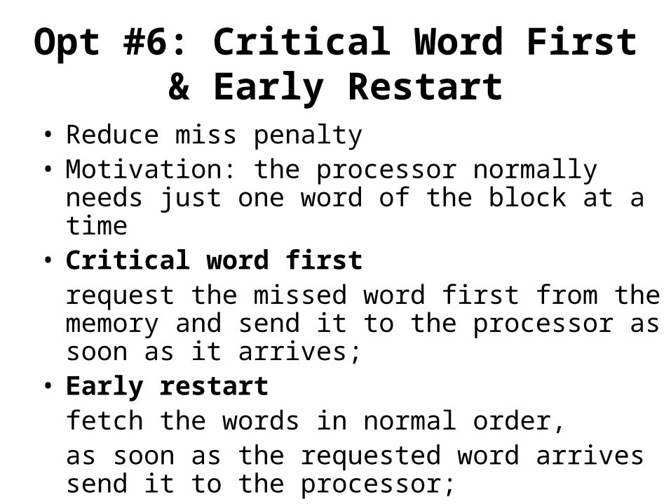
Opt #6: Critical Word First& Early Restart
• Reduce miss penalty• Motivation: the processor normally needs just
one word of the block at a time• Critical word first
request the missed word first from the memory and send it to the processor as soon as it arrives;
• Early restartfetch the words in normal order, as soon as the requested word arrives send it to the processor;
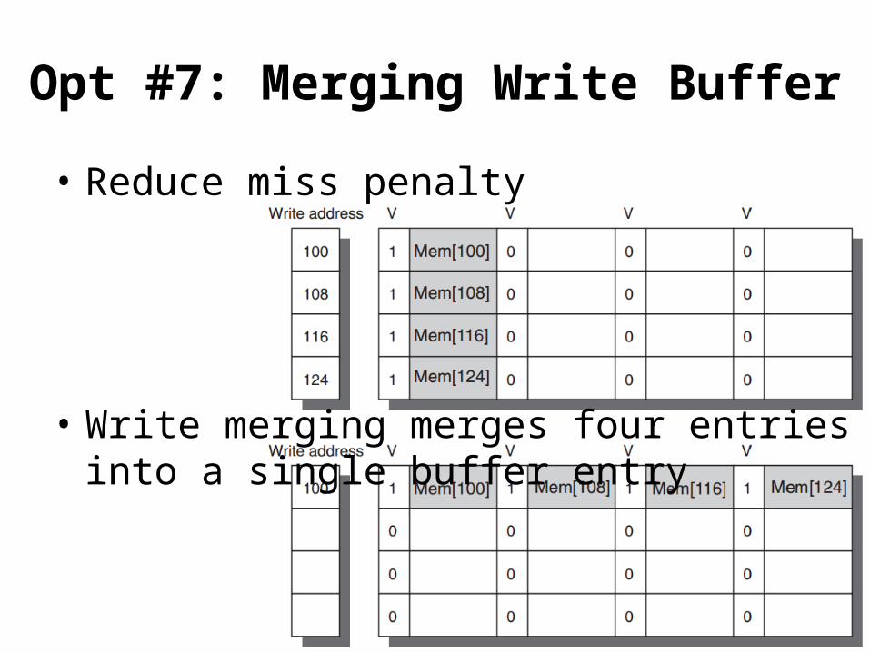
Opt #7: Merging Write Buffer
• Reduce miss penalty
• Write merging merges four entries into a single buffer entry
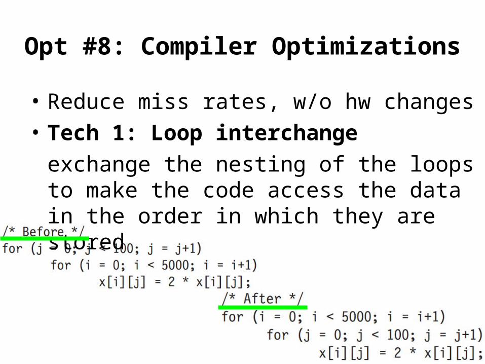
Opt #8: Compiler Optimizations
• Reduce miss rates, w/o hw changes• Tech 1: Loop interchange
exchange the nesting of the loops to make the code access the data in the order in which they are stored
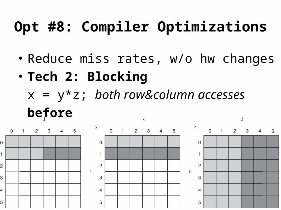
Opt #8: Compiler Optimizations
• Reduce miss rates, w/o hw changes• Tech 2: Blocking
x = y*z; both row&column accessesbefore
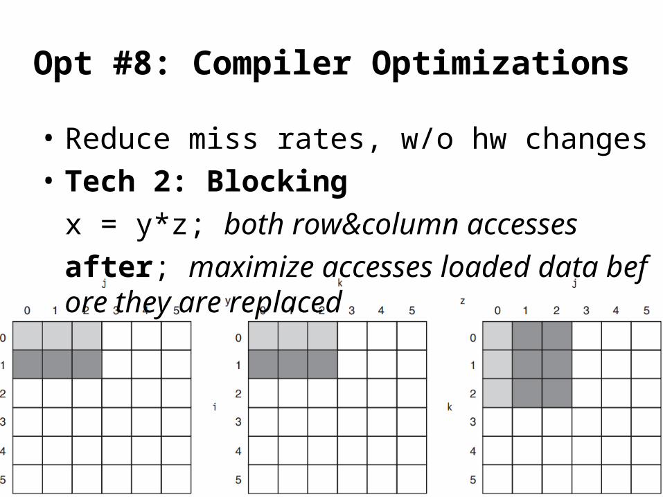
Opt #8: Compiler Optimizations
• Reduce miss rates, w/o hw changes• Tech 2: Blocking
x = y*z; both row&column accessesafter; maximize accesses loaded data before they are replaced
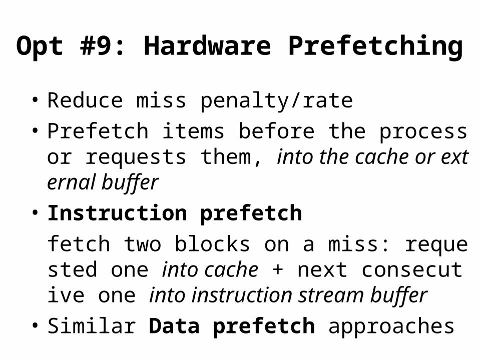
Opt #9: Hardware Prefetching
• Reduce miss penalty/rate• Prefetch items before the processor reque
sts them, into the cache or external buffer• Instruction prefetch
fetch two blocks on a miss: requested one into cache + next consecutive one into instruction stream buffer
• Similar Data prefetch approaches
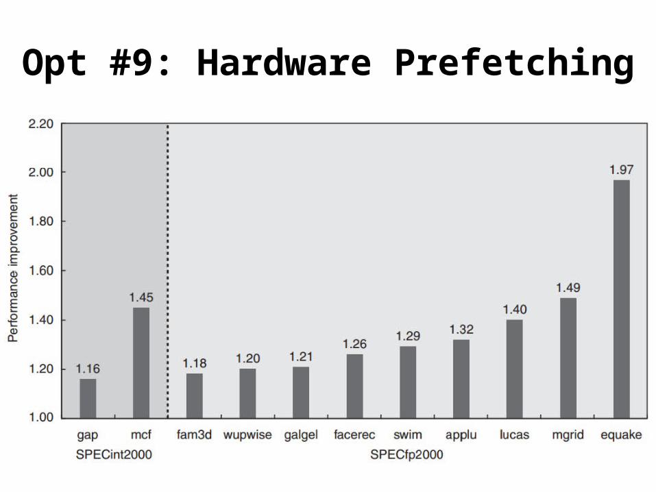
Opt #9: Hardware Prefetching
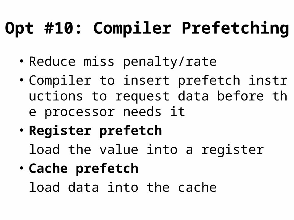
Opt #10: Compiler Prefetching
• Reduce miss penalty/rate• Compiler to insert prefetch instructions to
request data before the processor needs it• Register prefetch
load the value into a register• Cache prefetch
load data into the cache
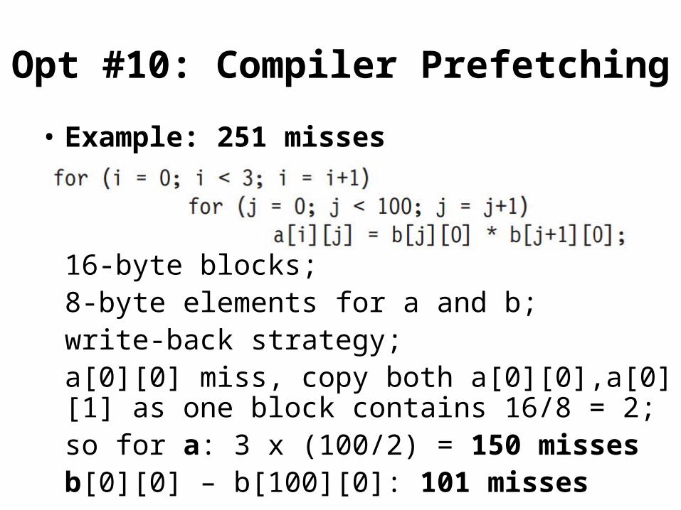
Opt #10: Compiler Prefetching
• Example: 251 misses
16-byte blocks;8-byte elements for a and b;write-back strategy;a[0][0] miss, copy both a[0][0],a[0][1] as one block contains 16/8 = 2;so for a: 3 x (100/2) = 150 missesb[0][0] – b[100][0]: 101 misses
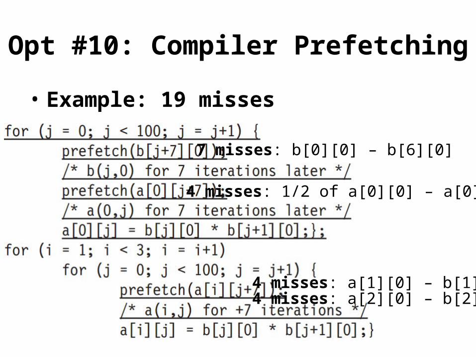
• Example: 19 misses
Opt #10: Compiler Prefetching
7 misses: b[0][0] – b[6][0]
4 misses: 1/2 of a[0][0] – a[0][6]
4 misses: a[1][0] – b[1][6]4 misses: a[2][0] – b[2][6]
Outline
• Ten Advanced Cache Optimizations• Memory Technology and Optimizations• Virtual Memory and Virtual Machines• ARM Cortex-A8 & Intel Core i7
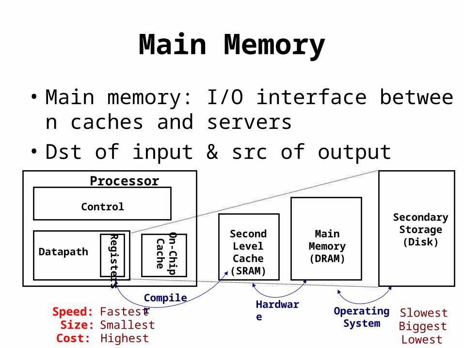
Main Memory
• Main memory: I/O interface between caches and servers
• Dst of input & src of output
Control
Datapath
SecondaryStorage(Disk)
Processor
Reg
isters
MainMemory(DRAM)
SecondLevelCache
(SRAM)
On
-Ch
ipC
ache
Fastest SlowestSmallest BiggestHighest Lowest
Speed:Size:
Cost:
CompilerHardware
Operating System
Main Memory
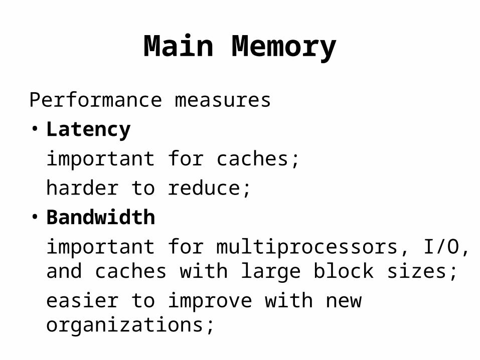
Performance measures• Latency
important for caches;harder to reduce;
• Bandwidthimportant for multiprocessors, I/O, and caches with large block sizes;easier to improve with new organizations;
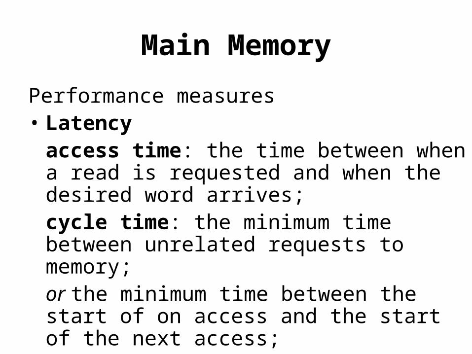
Main Memory
Performance measures• Latency
access time: the time between when a read is requested and when the desired word arrives;cycle time: the minimum time between unrelated requests to memory;or the minimum time between the start of on access and the start of the next access;
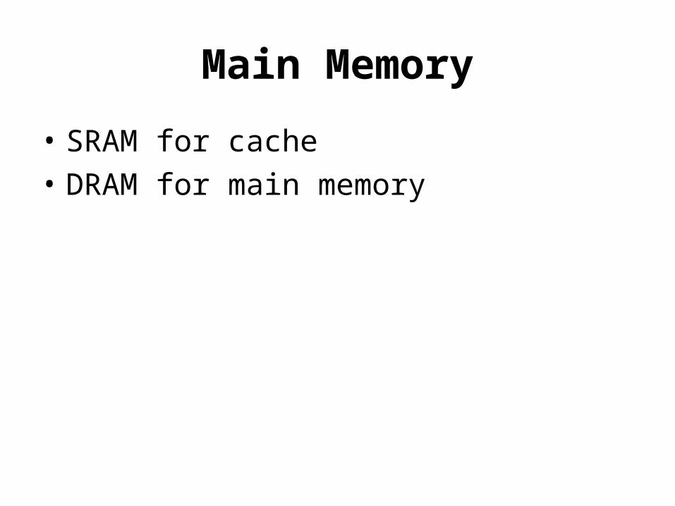
Main Memory
• SRAM for cache• DRAM for main memory
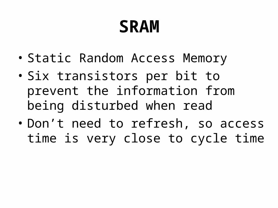
SRAM
• Static Random Access Memory• Six transistors per bit to prevent the
information from being disturbed when read
• Don’t need to refresh, so access time is very close to cycle time
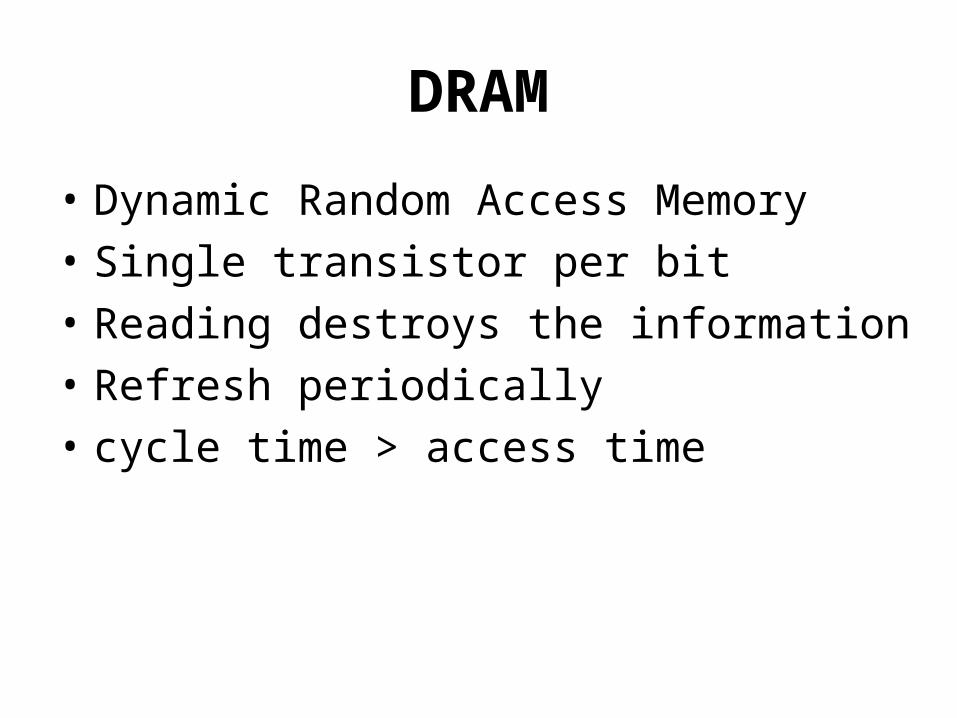
DRAM
• Dynamic Random Access Memory• Single transistor per bit• Reading destroys the information• Refresh periodically • cycle time > access time
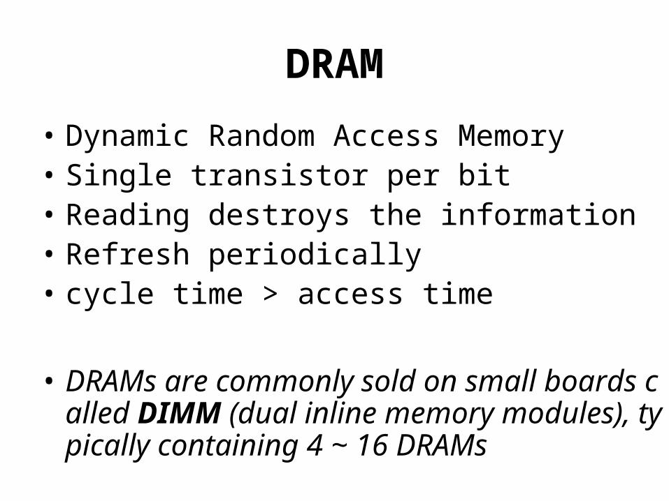
DRAM
• Dynamic Random Access Memory• Single transistor per bit• Reading destroys the information• Refresh periodically • cycle time > access time
• DRAMs are commonly sold on small boards called DIMM (dual inline memory modules), typically containing 4 ~ 16 DRAMs
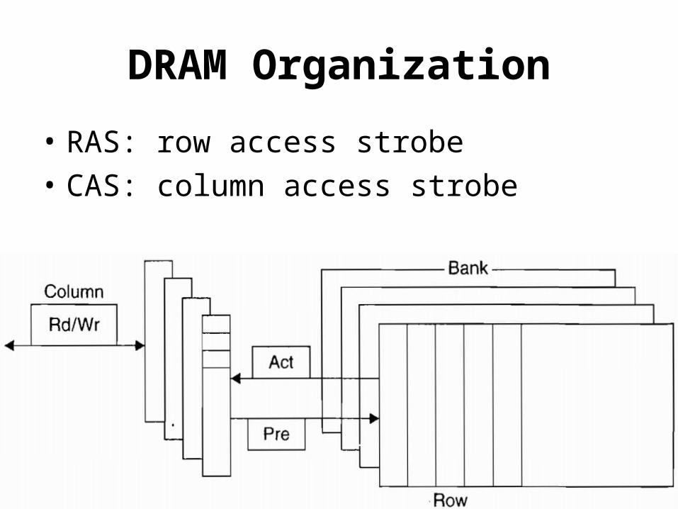
DRAM Organization
• RAS: row access strobe• CAS: column access strobe
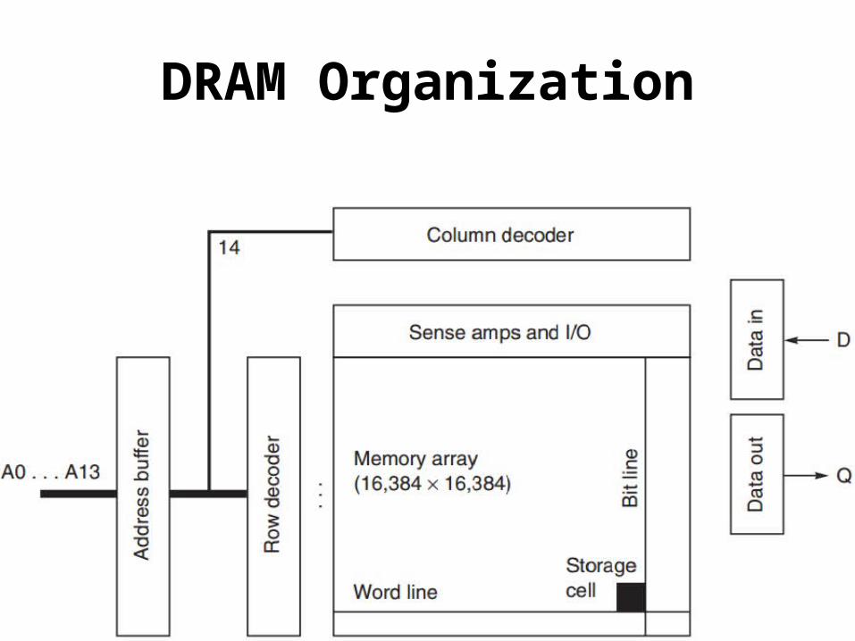
DRAM Organization
DRAM Improvement
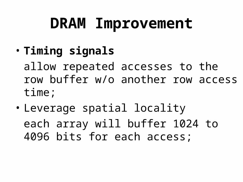
• Timing signalsallow repeated accesses to the row buffer w/o another row access time;
• Leverage spatial localityeach array will buffer 1024 to 4096 bits for each access;
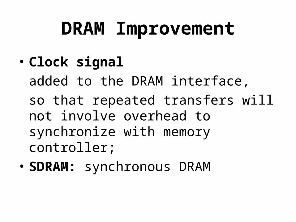
DRAM Improvement• Clock signal
added to the DRAM interface,so that repeated transfers will not involve overhead to synchronize with memory controller;
• SDRAM: synchronous DRAM
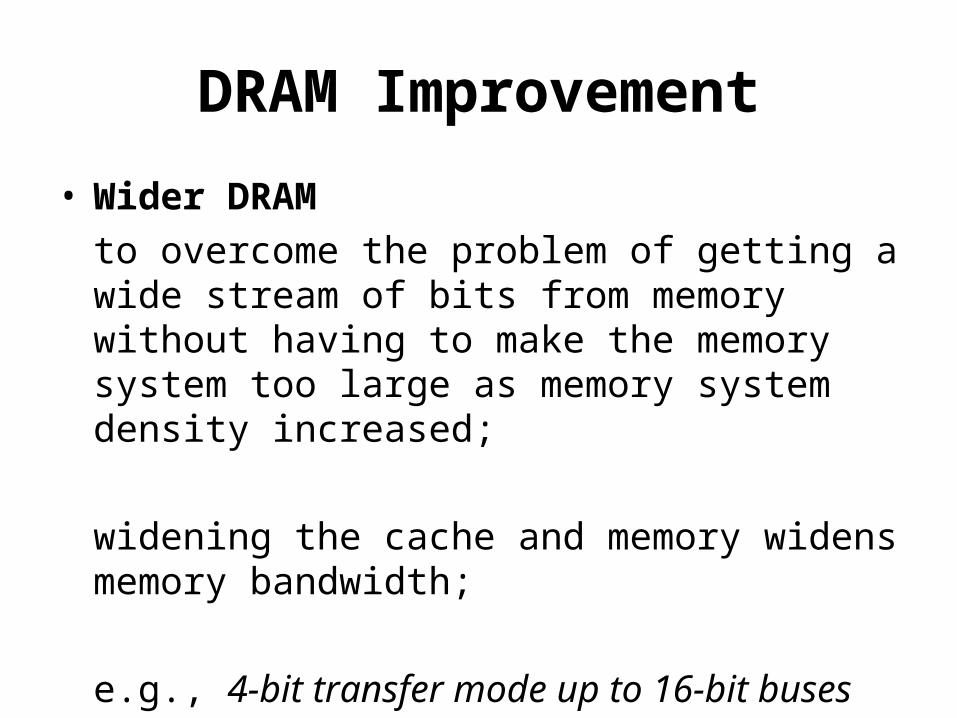
DRAM Improvement• Wider DRAM
to overcome the problem of getting a wide stream of bits from memory without having to make the memory system too large as memory system density increased;
widening the cache and memory widens memory bandwidth;
e.g., 4-bit transfer mode up to 16-bit buses
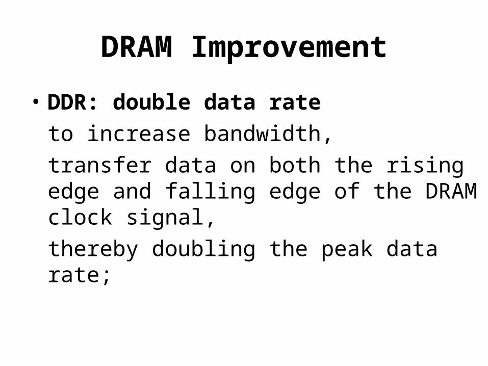
DRAM Improvement• DDR: double data rate
to increase bandwidth,transfer data on both the rising edge and falling edge of the DRAM clock signal,thereby doubling the peak data rate;
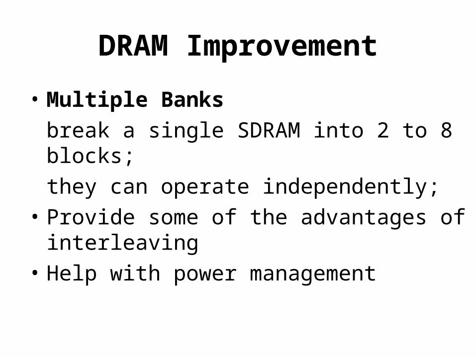
DRAM Improvement• Multiple Banks
break a single SDRAM into 2 to 8 blocks;they can operate independently;
• Provide some of the advantages of interleaving
• Help with power management
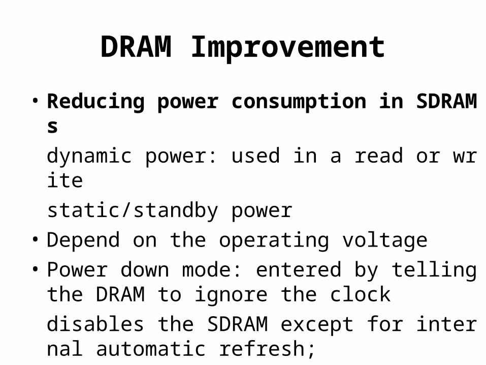
DRAM Improvement• Reducing power consumption in SDRAM
sdynamic power: used in a read or writestatic/standby power
• Depend on the operating voltage• Power down mode: entered by telling the
DRAM to ignore the clockdisables the SDRAM except for internal automatic refresh;
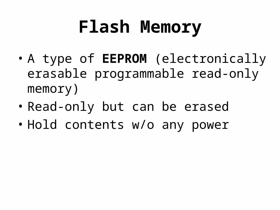
Flash Memory
• A type of EEPROM (electronically erasable programmable read-only memory)
• Read-only but can be erased• Hold contents w/o any power
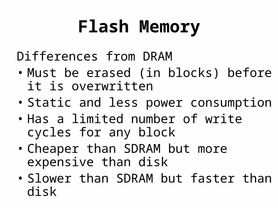
Flash Memory
Differences from DRAM• Must be erased (in blocks) before it is
overwritten• Static and less power consumption• Has a limited number of write cycles for
any block• Cheaper than SDRAM but more
expensive than disk• Slower than SDRAM but faster than disk
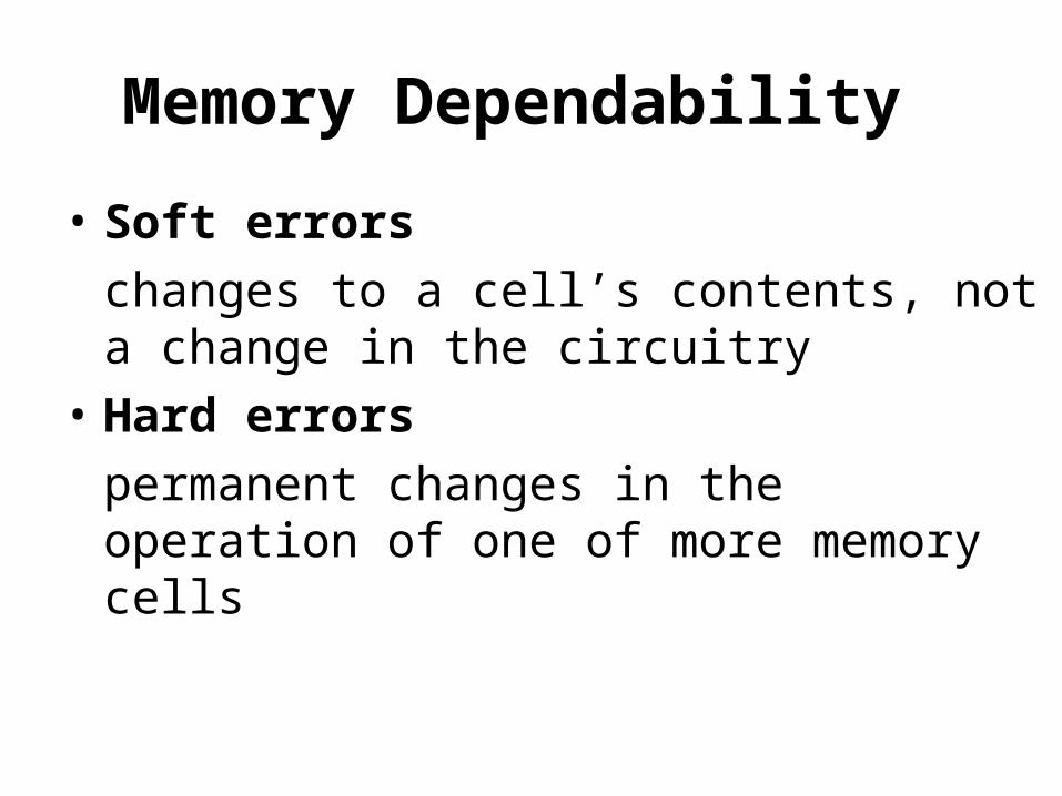
Memory Dependability
• Soft errorschanges to a cell’s contents, not a change in the circuitry
• Hard errorspermanent changes in the operation of one of more memory cells
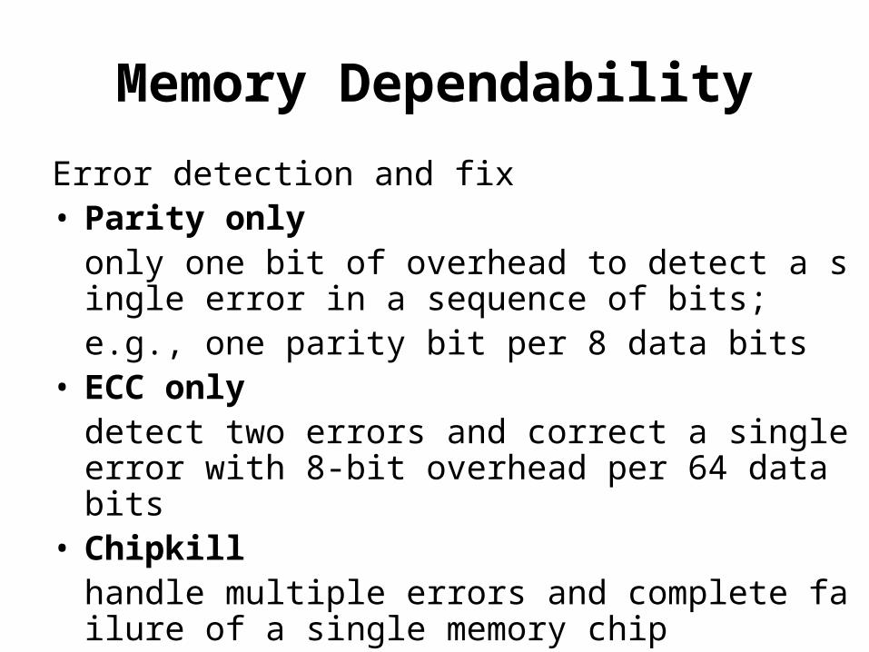
Memory DependabilityError detection and fix• Parity only
only one bit of overhead to detect a single error in a sequence of bits;e.g., one parity bit per 8 data bits
• ECC onlydetect two errors and correct a single error with 8-bit overhead per 64 data bits
• Chipkillhandle multiple errors and complete failure of a single memory chip
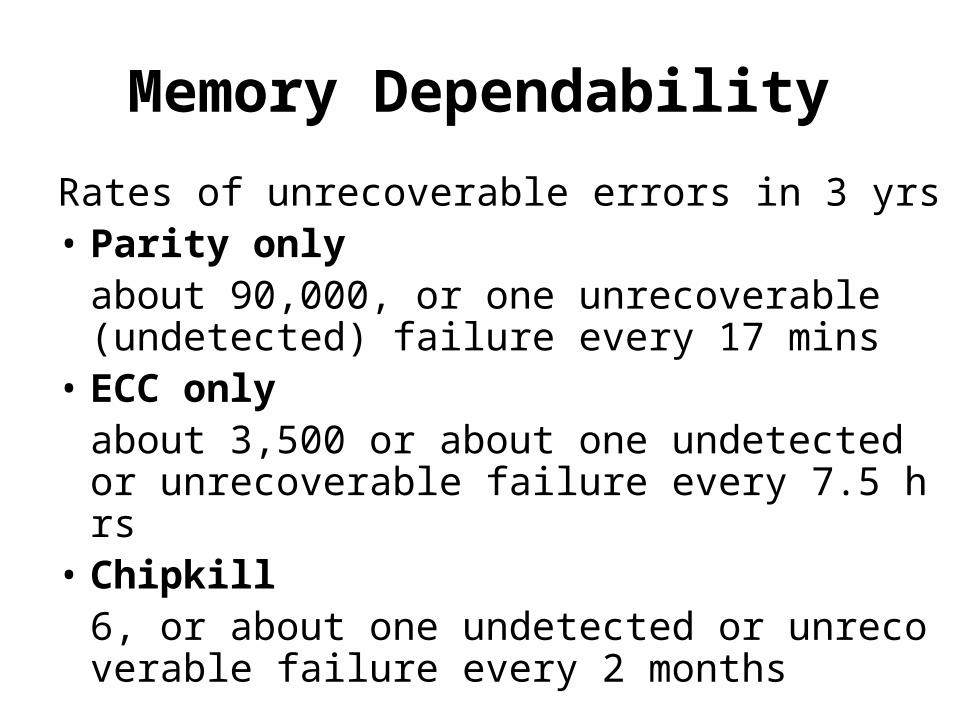
Memory DependabilityRates of unrecoverable errors in 3 yrs• Parity only
about 90,000, or one unrecoverable (undetected) failure every 17 mins
• ECC onlyabout 3,500 or about one undetected or unrecoverable failure every 7.5 hrs
• Chipkill6, or about one undetected or unrecoverable failure every 2 months
Outline
• Ten Advanced Cache Optimizations• Memory Technology and Optimizations• Virtual Memory and Virtual Machines• ARM Cortex-A8 & Intel Core i7
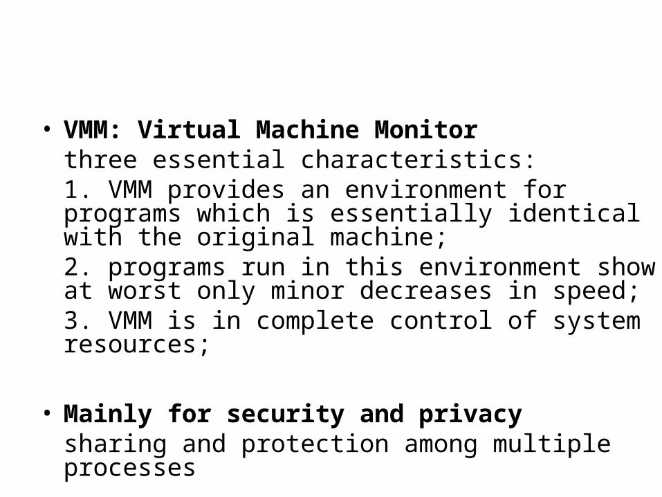
• VMM: Virtual Machine Monitorthree essential characteristics:1. VMM provides an environment for programs which is essentially identical with the original machine;2. programs run in this environment show at worst only minor decreases in speed;3. VMM is in complete control of system resources;
• Mainly for security and privacysharing and protection among multiple processes
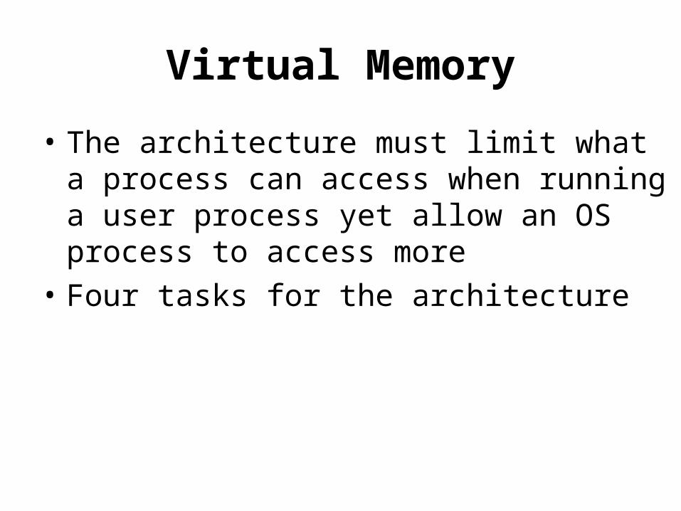
Virtual Memory
• The architecture must limit what a process can access when running a user process yet allow an OS process to access more
• Four tasks for the architecture
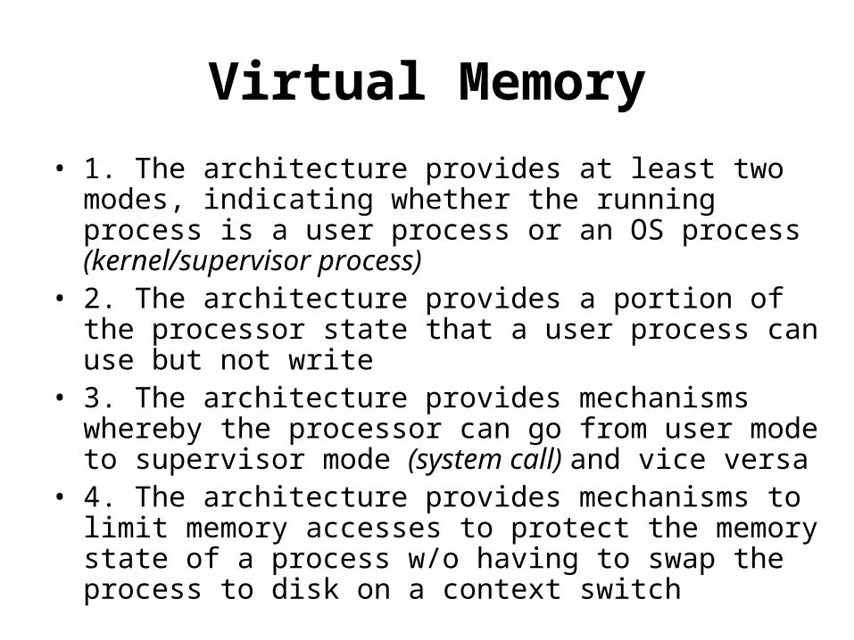
Virtual Memory• 1. The architecture provides at least two modes,
indicating whether the running process is a user process or an OS process (kernel/supervisor process)
• 2. The architecture provides a portion of the processor state that a user process can use but not write
• 3. The architecture provides mechanisms whereby the processor can go from user mode to supervisor mode (system call) and vice versa
• 4. The architecture provides mechanisms to limit memory accesses to protect the memory state of a process w/o having to swap the process to disk on a context switch
Virtual Machines
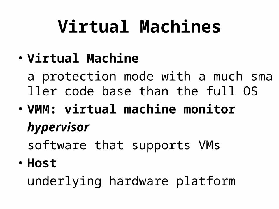
• Virtual Machinea protection mode with a much smaller code base than the full OS
• VMM: virtual machine monitorhypervisorsoftware that supports VMs
• Hostunderlying hardware platform
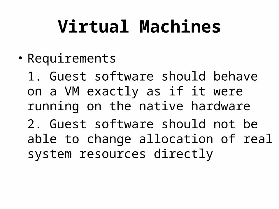
Virtual Machines• Requirements
1. Guest software should behave on a VM exactly as if it were running on the native hardware2. Guest software should not be able to change allocation of real system resources directly
Outline
• Ten Advanced Cache Optimizations• Memory Technology and Optimizations• Virtual Memory and Virtual Machines• ARM Cortex-A8 & Intel Core i7
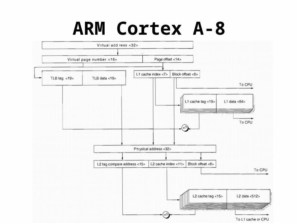
ARM Cortex A-8
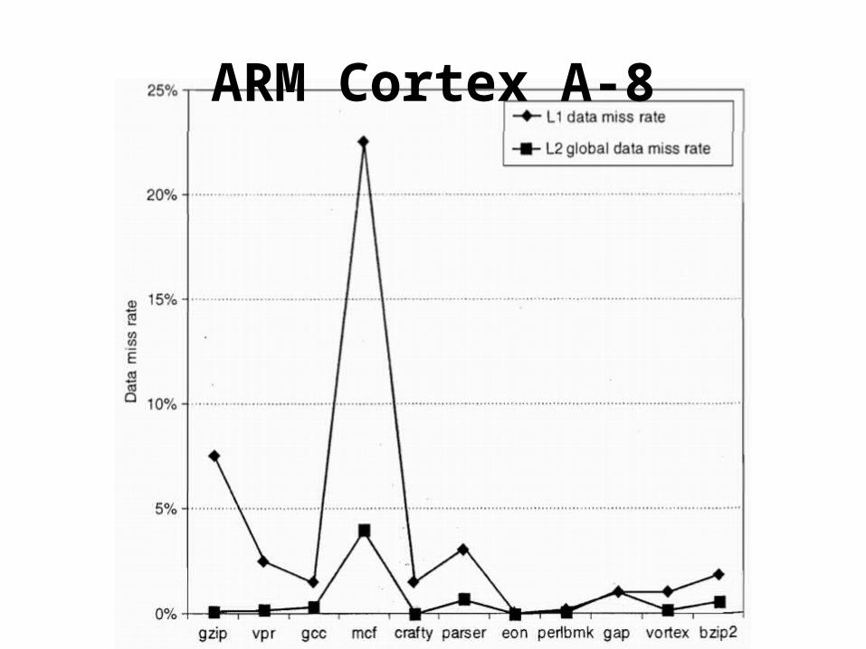
ARM Cortex A-8
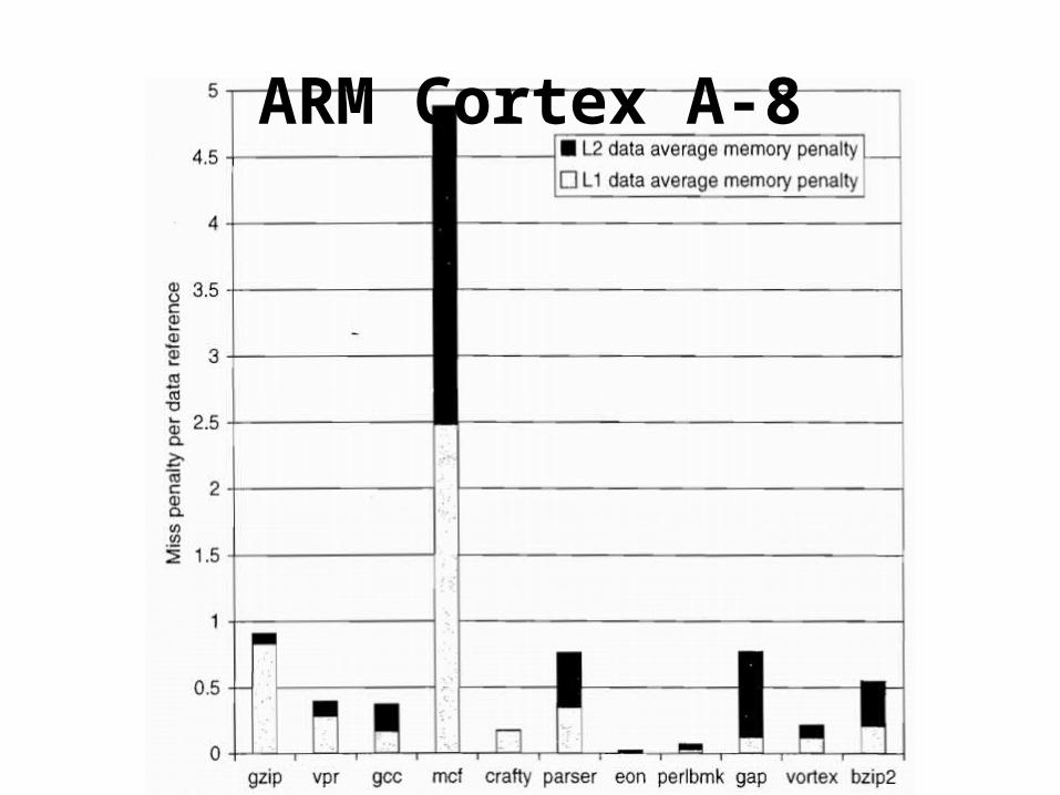
ARM Cortex A-8
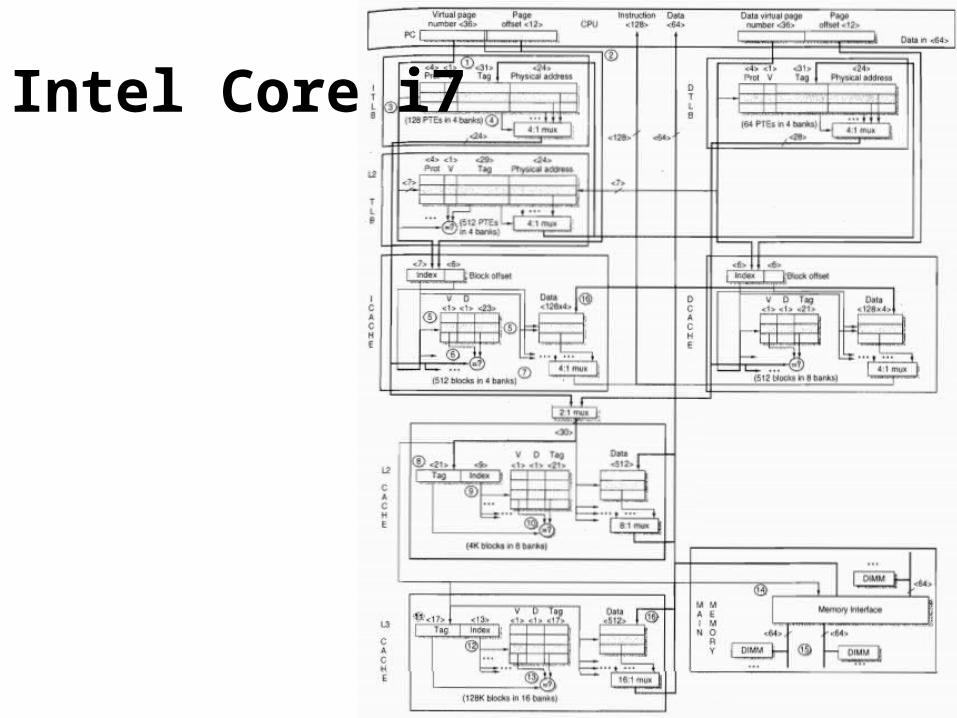
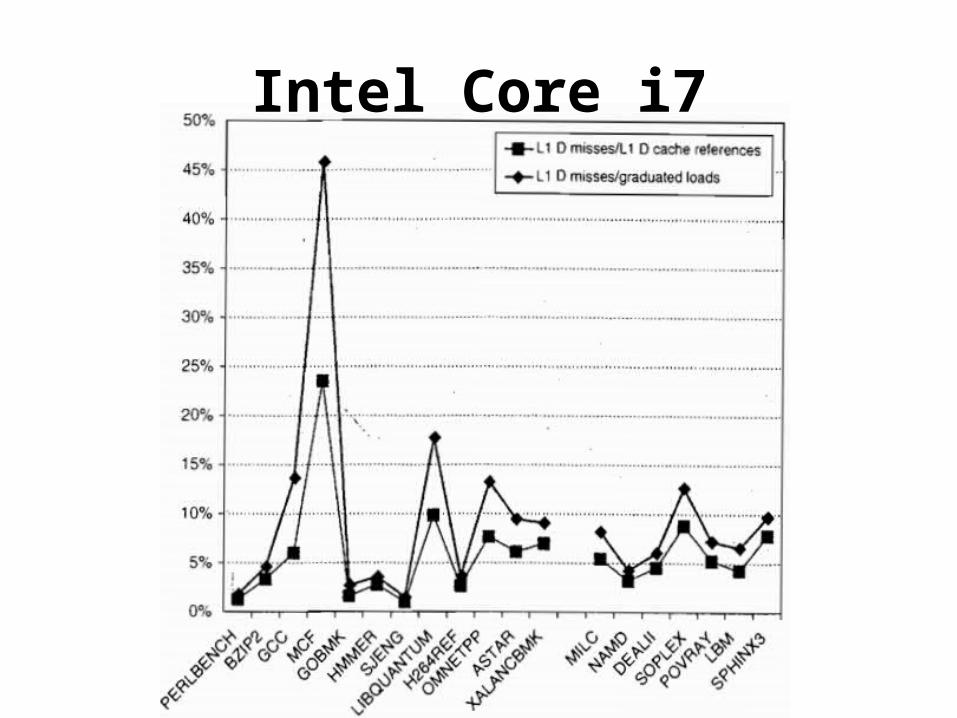
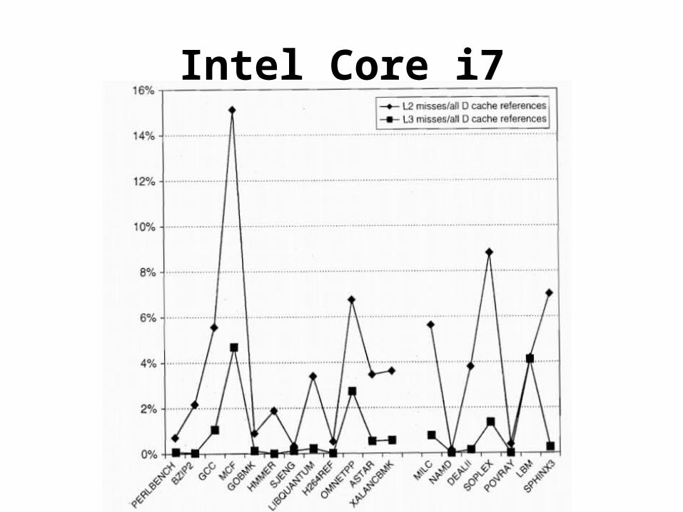
Intel Core i7
Intel Core i7
Intel Core i7

?