Embed Size (px)
Citation preview
Digital logic
Lecture 1.Introduction
Doru Todinca
Department of Computers
Politehnica University of Timisoara
Outline
Principles and practice
Analog versus digital
Digital devices
Electronic aspects of digital devicesLogic levels, invalid levels and noise marginsLogic families: CMOS family
Integrated circuits
Digital-Design Levels

Administrative
◮ Instructor: Doru Todinca, room B622
◮ e-mail: [email protected]
◮ web page: www.cs.upt.ro/~todinca/DL
◮ Labs are mandatory and will count 50% in the final mark
◮ The lecture is also mandatory
◮ Examination: written exam, counting 50% of the final grade
Outline
Principles and practice
Analog versus digital
Digital devices
Electronic aspects of digital devicesLogic levels, invalid levels and noise marginsLogic families: CMOS family
Integrated circuits
Digital-Design Levels
Textbook
◮ Textbook: John F. Wakerly, Digital Design: Principles
and Practice, Third Edition, Prentice Hall, Inc, 2000
◮ The fourth edition was published in 2006
◮ Third edition of Wakerly’s textbook was translated inRomanian: “Cicuite digitale: Principiile si practicile folisite inproiectare”, Teora, 2002, ISBN 973-20-0659-5
◮ My presentations are entirely based on John Wakerly’s book
◮ in the sense that figures, tables, definitions, examples, etc,from third edition are used for these presentations
◮ Handouts will be enough for your exam, but Wakerly’s bookmay be useful.

Principles and practice
◮ Most of the principles that you learn now will continue to beimportant in the future
◮ Maybe some principles will be applied in ways that have notyet been discovered!
◮ Practice changes much faster, sometimes even before youstart working in the field
◮ For sure many practical things will change through your career
◮ Wakerly: “Treat practice material as a way to reinforceprinciples
◮ and as a way to learn design methods by examples”.
◮ These things are valid not only for Digital Logic, but for mostthings that you study in college !
Outline
Principles and practice
Analog versus digital
Digital devices
Electronic aspects of digital devicesLogic levels, invalid levels and noise marginsLogic families: CMOS family
Integrated circuits
Digital-Design Levels
Analog versus digital
◮ Analog signals (produced by analog devices) can take anyvalue over a continuous range of values (of voltage, current,or other metric)
◮ We model a digital signal as taking at any time only twodiscrete values
◮ We call these two values 0 and 1, LOW and HIGH, FALSEand TRUE, negated or asserted, etc.
◮ In reality digital signals do take values over a continuousrange of voltages, currents, etc, but we ignore their analogbehaviour.
◮ Digital abstraction: we associate a range of analog valueswith a logic 0 value and another range of analog value witha logic 1.
◮ The range of values associated to 0 logic and the range ofvalues associated to 1 logic are separated by a range of invalid(undefined) values
Analog versus digital: advantages of digital devices
◮ Reproducibility of results:◮ a properly designed digital device always obtains the same
results (outputs) for the same set of inputs◮ For an analog circuit this not always true, because its outputs
can vary with temperature, power supply, aging, and otherfactors
◮ Ease of design: Digital, or logic design is logic, no specialmath needed (e.g. calculus)
◮ Flexibility and functionality: once a problem is in digital form,we can follow a set of logical steps and solve it.
◮ Programmability:◮ much of digital design is done using Hardware Description
Languages (HDLs).◮ HDLs are used for modeling, simulation and synthesis◮ The use of HDLs in digital design will increase even more in
the future
◮ Speed: digital circuits are very fast
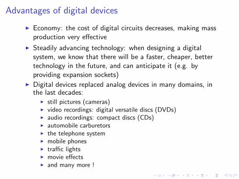
Advantages of digital devices
◮ Economy: the cost of digital circuits decreases, making massproduction very effective
◮ Steadily advancing technology: when designing a digitalsystem, we know that there will be a faster, cheaper, bettertechnology in the future, and can anticipate it (e.g. byproviding expansion sockets)
◮ Digital devices replaced analog devices in many domains, inthe last decades:
◮ still pictures (cameras)◮ video recordings: digital versatile discs (DVDs)◮ audio recordings: compact discs (CDs)◮ automobile carburetors◮ the telephone system◮ mobile phones◮ traffic lights◮ movie effects◮ and many more !
Outline
Principles and practice
Analog versus digital
Digital devices
Electronic aspects of digital devicesLogic levels, invalid levels and noise marginsLogic families: CMOS family
Integrated circuits
Digital-Design Levels
Digital devices. Combinational and sequential devices
There are two types of digital devices: combinational devices andsequential devices
DefinitionCombinational devices: their outputs depend only on the currentinput combination (i.e., the combination of their input values)
DefinitionSequential devices: their outputs depend on the current inputcombination and the sequence of past inputs.
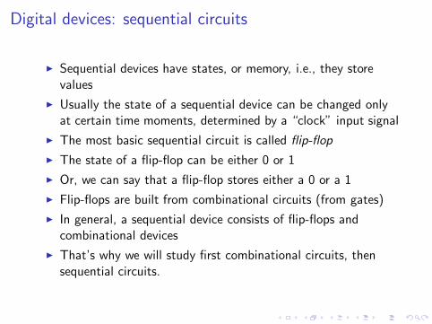
Digital devices: sequential circuits
◮ Sequential devices have states, or memory, i.e., they storevalues
◮ Usually the state of a sequential device can be changed onlyat certain time moments, determined by a “clock” input signal
◮ The most basic sequential circuit is called flip-flop
◮ The state of a flip-flop can be either 0 or 1
◮ Or, we can say that a flip-flop stores either a 0 or a 1
◮ Flip-flops are built from combinational circuits (from gates)
◮ In general, a sequential device consists of flip-flops andcombinational devices
◮ That’s why we will study first combinational circuits, thensequential circuits.
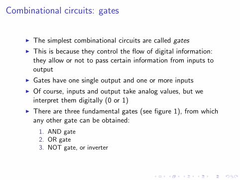
Combinational circuits: gates
◮ The simplest combinational circuits are called gates
◮ This is because they control the flow of digital information:they allow or not to pass certain information from inputs tooutput
◮ Gates have one single output and one or more inputs
◮ Of course, inputs and output take analog values, but weinterpret them digitally (0 or 1)
◮ There are three fundamental gates (see figure 1), from whichany other gate can be obtained:
1. AND gate2. OR gate3. NOT gate, or inverter

Combinational circuits: gates
(c) 1
(a) 00
0
(b) 00
0
0 0
00
1
10
1
1
01
0
11
0
11
1
11
1
Copyright © 2000 by Prentice Hall, Inc. Digital Design Principles and Practices, 3/e
Figure 1 : Digital devices: (a) AND gate, (b) OR gate and (c) NOTgate, or inverter
Figure 1 shows the symbols of the three fundamental gates, andtheir behaviour: all input combinations and the resulting outputs.

Digital gates and truth tables
(c)
X NOT X
1
0 1
0
NOT XX(a)
X
0
1
X AND YY
0
1
1
0
1
0
0
0
0
1
X AND YX
Y (b)
X
0
1
X OR YY
0
1
1
0
1
0
0
1
1
1
X OR Y
X′ X • Y X + Y
X
Y
Copyright © 2000 by Prentice Hall, Inc. Digital Design Principles and Practices, 3/e
Figure 2 : Fundamental gates and truth tables: (a) for AND gate, (b)for OR gate, (c) for NOT gate
A gate’s behaviour can be expressed more compactly using thetruth table (see figure 2)The figure shows also the functions realized by the three gates: XAND Y, X OR Y, and NOT X
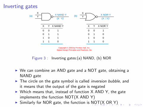
Inverting gates
(a)
X
0
1
X NAND YY
0
1
1
0
1
0
1
1
1
0
X NAND YX
Y (b)
X
0
1
X NOR YY
0
1
1
0
1
0
1
0
0
0
X NOR Y
(X • Y)′ (X + Y)′
X
Y
Copyright © 2000 by Prentice Hall, Inc. Digital Design Principles and Practices, 3/e
Figure 3 : Inverting gates:(a) NAND, (b) NOR
◮ We can combine an AND gate and a NOT gate, obtaining aNAND gate
◮ The circle on the gate symbol is called inversion bubble, andit means that the output of the gate is negated
◮ Which means that, instead of function X AND Y, the gateimplements the function NOT(X AND Y)
◮ Similarly for NOR gate, the function is NOT(X OR Y)

Logic values, logic signals and gates. Definitions
◮ A logic value, 0 or 1, is called a binary digit, or bit.
◮ If more than two values are needed, then we can add morebits.
◮ With n bits we have 2n different values.
◮ When we discuss electronic logic circuits we use LOW andHIGH for 0 and 1.
◮ LOW: a signal is in the range of algebraically lower values,which is interpreted as logic 0.
◮ HIGH a signal is in the range of algebraically higher values,which is interpreted as logic 1
◮ Association between 0 and LOW and 1 and HIGH is arbitrary,and is called positive logic.
◮ The opposite association, i.e., 0 to HIGH and 1 to LOW iscalled negative logic. Normally we use positive logic.
Logic values, logic signals and gates. Definitions
◮ The operation of a combinational circuit is fully described bya truth table that lists all combinations of input values andthe output value(s) produced by each input combination.
◮ For a combinational circuit with n inputs, the truth table has2n lines.
◮ The behaviour of a sequential circuit can be described by astate table
◮ The state table specifies next state and the output as functionof its inputs and current state.

Logic values, logic signals and gates. Definitions
◮ An AND gate produces a 1 output if and only if (iff) all itsinputs are 1. Otherwise its output is 0.
◮ It means that, if at least one input is 0, the output of an ANDgate is 0.
◮ The output function of an AND gate with inputs X and Y isdenoted X AND Y or X · Y .
◮ An OR gate produces a 1 output if and only if one or moreinputs are 1.
◮ It means that an OR gate produces a 0 output iff all inputsare 0.
◮ The function of an OR gate with inputs X and Y is denoted XOR Y or X + Y .
Logic values, logic signals and gates. Definitions
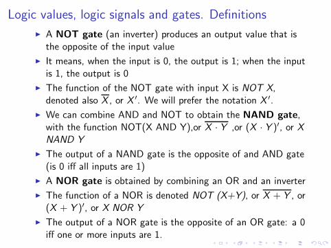
◮ A NOT gate (an inverter) produces an output value that isthe opposite of the input value
◮ It means, when the input is 0, the output is 1; when the inputis 1, the output is 0
◮ The function of the NOT gate with input X is NOT X,denoted also X , or X ′. We will prefer the notation X ′.
◮ We can combine AND and NOT to obtain the NAND gate,with the function NOT(X AND Y),or X · Y ,or (X · Y )′, or XNAND Y
◮ The output of a NAND gate is the opposite of and AND gate(is 0 iff all inputs are 1)
◮ A NOR gate is obtained by combining an OR and an inverter
◮ The function of a NOR is denoted NOT (X+Y), or X + Y , or(X + Y )′, or X NOR Y
◮ The output of a NOR gate is the opposite of an OR gate: a 0iff one or more inputs are 1.
Representations of a digital device
1. The “black-box” representation (fig 4):
◮ Minimum amount of detail: only the number of inputs andoutputs
◮ It does not describe the functioning of the device (how itresponds to input signals
2. The truth table: for combinational circuits (fig 5)
3. Logic diagram (logic circuit) (fig 6): we will learn how toobtain the logic circuit from the truth table
4. Timing diagram (fig 7):
◮ Contains the time dimension of the circuit’s behaviour◮ It shows how the circuit might respond to the time-varying
input signals◮ It shows also that the logic signals do not change
instantaneously from logic 0 to logic 1: the signals have aslope, visible on the oscilloscope, but not in simulation
◮ Also, we can see that there is a lag between an input changeand the corresponding output change (circuit’s delay): it canbe visualized by simulation
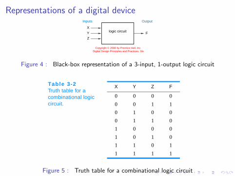
Representations of a digital device
logic circuitX
Y
Z
F
Inputs Output
Copyright © 2000 by Prentice Hall, Inc. Digital Design Principles and Practices, 3/e
Figure 4 : Black-box representation of a 3-input, 1-output logic circuit
Table 3-2Truth table for a combinational logic circuit.
X Y Z F
0 0 0 0
0 0 1 1
0 1 0 0
0 1 1 0
1 0 0 0
1 0 1 0
1 1 0 1
1 1 1 1
Figure 5 : Truth table for a combinational logic circuit
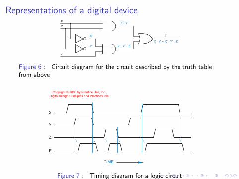
Representations of a digital deviceX
Y
Z
F
X • Y
X′ • Y′ • Z
X′
Y′ X • Y + X′ • Y′ • Z
Figure 6 : Circuit diagram for the circuit described by the truth tablefrom above
X
Y
Z
F
TIME
Copyright © 2000 by Prentice Hall, Inc. Digital Design Principles and Practices, 3/e
Figure 7 : Timing diagram for a logic circuit
Outline
Principles and practice
Analog versus digital
Digital devices
Electronic aspects of digital devicesLogic levels, invalid levels and noise marginsLogic families: CMOS family
Integrated circuits
Digital-Design Levels

Logic values and undefined values
5.0 V
3.5 V
1.5 V
0.0 V
Logic 1 (HIGH)
Logic 0 (LOW)
undefinedlogic level
Copyright © 2000 by Prentice Hall, Inc. Digital Design Principles and Practices, 3/e
Figure 8 : Logic levels for CMOScircuits
◮ Between 0.0 V and 1.5 V isthe voltage intervalrepresenting logic 0 values
◮ Between 3.5 V and 5.0 V isthe voltage intervalrepresenting logic 1 values.
◮ Between the 0 logic valuesand 1 logic values is theinterval for undefined(invalid) values: the interval1.5 V to 3.5 V.
◮ The values are for theCMOS integrated circuits.
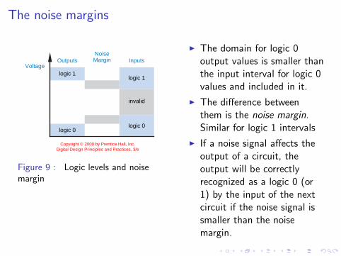
The noise margins
logic 0
Outputs InputsNoiseMargin
Voltagelogic 1
logic 0
logic 1
invalid
Copyright © 2000 by Prentice Hall, Inc. Digital Design Principles and Practices, 3/e
Figure 9 : Logic levels and noisemargin
◮ The domain for logic 0output values is smaller thanthe input interval for logic 0values and included in it.
◮ The difference betweenthem is the noise margin.Similar for logic 1 intervals
◮ If a noise signal affects theoutput of a circuit, theoutput will be correctlyrecognized as a logic 0 (or1) by the input of the nextcircuit if the noise signal issmaller than the noisemargin.

Logic families
◮ First electronically controlled logic circuits were based onrelays (1930, Bell Labs)
◮ Eniac, first electronic digital computer was built with vacuumtubes (mid-1940s)
◮ Invention of semiconductor diode and bipolar junctiontransistor made computers smaller and faster (late 1950s)
◮ In 1960s: invention of integrated circuit (IC): multiple diodes,transistors and other components on a single chip
◮ Definition: “a logic family is a collection of differentintegrated circuit chips that have similar input, output, andinternal circuit characteristics, but that perform different logicfunctions”
◮ Most successful bipolar logic family: transistor-transistor logic(TTL) 1960s
◮ Metal oxide semiconductor field-effect transistor (MOSFET,or MOS transistor): the base of CMOS family (mid 1980’s)
◮ CMOS technology: most used and easiest to understand !
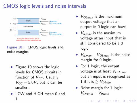
CMOS logic levels and noise intervals
High-stateDC noise margin
Low-stateDC noise margin
0.7 VCC
0.3 VCC
VCC
0
VIHmin
VOHmin
VOLmax
VILmax
HIGH
ABNORMAL
LOW
Copyright © 2000 by Prentice Hall, Inc. Digital Design Principles and Practices, 3/e
Figure 10 : CMOS logic levels andnoise margins
◮ Figure 10 shows the logiclevels for CMOS circuits infunction of VCC . UsuallyVCC = 5.0V , but it can besmaller.
◮ LOW and HIGH mean 0 and1
◮ VOLmax is the maximumoutput voltage that anoutput in 0 logic can have
◮ VILmax is the maximumvoltage at an input that isstill considered to be a 0logic
◮ VILmax −VOLmax is the noisemargin for 0 logic.
◮ For 1 logic, the outputvoltage is at least VOHmin,but an input is recognized as1 if it is ≥ VIHmin
◮ Noise margin for 1 logic:VOHmin − VIHmin
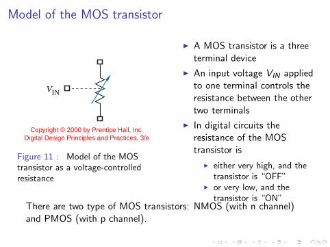
Model of the MOS transistor
VIN
Copyright © 2000 by Prentice Hall, Inc. Digital Design Principles and Practices, 3/e
Figure 11 : Model of the MOStransistor as a voltage-controlledresistance
◮ A MOS transistor is a threeterminal device
◮ An input voltage VIN appliedto one terminal controls theresistance between the othertwo terminals
◮ In digital circuits theresistance of the MOStransistor is
◮ either very high, and thetransistor is “OFF”
◮ or very low, and thetransistor is “ON”
There are two type of MOS transistors: NMOS (with n channel)and PMOS (with p channel).
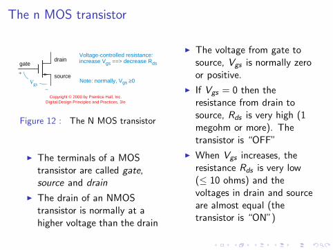
The n MOS transistor
gatedrain
source
Voltage-controlled resistance:increase Vgs ==> decrease Rds
Note: normally, Vgs ≥0� Vgs
+
−Copyright © 2000 by Prentice Hall, Inc.
Digital Design Principles and Practices, 3/e
Figure 12 : The N MOS transistor
◮ The terminals of a MOStransistor are called gate,source and drain
◮ The drain of an NMOStransistor is normally at ahigher voltage than the drain
◮ The voltage from gate tosource, Vgs is normally zeroor positive.
◮ If Vgs = 0 then theresistance from drain tosource, Rds is very high (1megohm or more). Thetransistor is “OFF”
◮ When Vgs increases, theresistance Rds is very low(≤ 10 ohms) and thevoltages in drain and sourceare almost equal (thetransistor is “ON”)
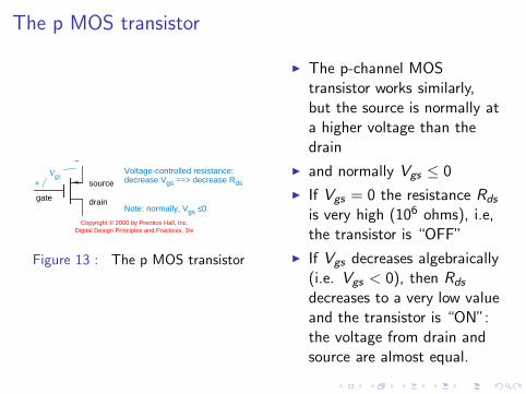
The p MOS transistor
gate drain
source
Voltage-controlled resistance:decrease Vgs ==> decrease Rds
Note: normally, Vgs ≤ 0
Vgs+
−
Copyright © 2000 by Prentice Hall, Inc. Digital Design Principles and Practices, 3/e
Figure 13 : The p MOS transistor
◮ The p-channel MOStransistor works similarly,but the source is normally ata higher voltage than thedrain
◮ and normally Vgs ≤ 0
◮ If Vgs = 0 the resistance Rds
is very high (106 ohms), i.e,the transistor is “OFF”
◮ If Vgs decreases algebraically(i.e. Vgs < 0), then Rds
decreases to a very low valueand the transistor is “ON”:the voltage from drain andsource are almost equal.

CMOS NOT gate
VIN
VDD = +5.0 V
VOUT
Q2(p-channel)
Q1(n-channel)
0.05.0
VIN
(L)(H)
(H)(L)
Q1
offon
Q2
onoff
5.00.0
VOUT(b)
(c)
(a)
IN OUT
Copyright © 2000 by Prentice Hall, Inc. Digital Design Principles and Practices, 3/e
Figure 14 : CMOS NOT gate (inverter): (a) circuit diagram; (b)functional behaviour; (c) logic symbol
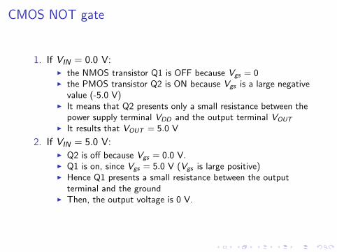
CMOS NOT gate
1. If VIN = 0.0 V:◮ the NMOS transistor Q1 is OFF because Vgs = 0◮ the PMOS transistor Q2 is ON because Vgs is a large negative
value (-5.0 V)◮ It means that Q2 presents only a small resistance between the
power supply terminal VDD and the output terminal VOUT
◮ It results that VOUT = 5.0 V
2. If VIN = 5.0 V:◮ Q2 is off because Vgs = 0.0 V.◮ Q1 is on, since Vgs = 5.0 V (Vgs is large positive)◮ Hence Q1 presents a small resistance between the output
terminal and the ground◮ Then, the output voltage is 0 V.

CMOS NOT gate
VDD = +5.0 V
VOUT = HVIN = L
(a)VDD = +5.0 V
VOUT = LVIN = H
(b)
Copyright © 2000 by Prentice Hall, Inc. Digital Design Principles and Practices, 3/e
Figure 15 : Switch model for CMOS NOT gate: (a) LOW input; (b)HIGH input
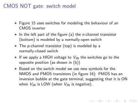
CMOS NOT gate: switch model
◮ Figure 15 uses switches for modeling the behaviour of anCMOS inverter
◮ In the left part of the figure (a) the n-channel transistor(bottom) is modeled by a normally-open switch
◮ The p-channel transistor (top) is modeled by anormally-closed switch
◮ If we apply a HIGH voltage to VIN the switches go to theopposite position (as shown in (b))
◮ Based on the switch model we use new symbols for theNMOS and PMOS transistors (in figure 16): PMOS has aninversion bubble at the gate terminal, suggesting that it is ONwhen VIN is LOW (when VIN is negative).
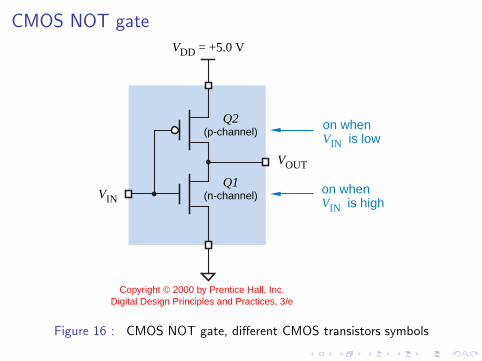
CMOS NOT gate
Q2(p-channel)
VIN
VDD = +5.0 V
VOUT
Q1(n-channel)
on whenVIN is low
on whenVIN is high
Copyright © 2000 by Prentice Hall, Inc. Digital Design Principles and Practices, 3/e
Figure 16 : CMOS NOT gate, different CMOS transistors symbols
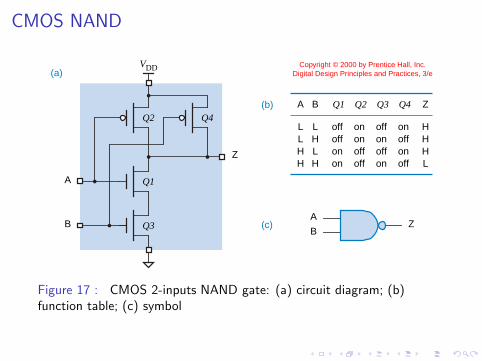
CMOS NAND
VDD
A
B
Z
Q1
Q3
Q2 Q4
A
LLHH
B
LHLH
Q1
offoffonon
Q2
ononoffoff
Q3
offonoffon
Q4
onoffonoff
Z
HHHL
A
BZ
(a)
(b)
(c)
Copyright © 2000 by Prentice Hall, Inc. Digital Design Principles and Practices, 3/e
Figure 17 : CMOS 2-inputs NAND gate: (a) circuit diagram; (b)function table; (c) symbol
CMOS NAND
◮ Circuit diagram of CMOS NAND gate is shown in figure 17
◮ When at least one input is LOW (0.0 V):◮ the corresponding PMOS transistor(s) will be ON and a path
is open between VDD to output Z◮ It results that Z is HIGH◮ The path between Z and ground is blocked because at least
one NMOS transistor is OFF
◮ When both inputs are HIGH (5.0 V):◮ both PMOS transistors are OFF◮ then, the path between VDD and Z is blocked◮ but, both NMOS transistors are ON◮ which means that the path between ground and Z is open◮ hence Z is LOW◮ A switch model of the 2-inputs NAND gate is shown next (in
fig 18)
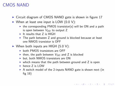
CMOS NAND
VDD
A = L
Z = H
(a)
B = L
VDD
A = H
Z = H
(b)
B = L
VDD
A = H
Z = L
(c)
B = H
Copyright © 2000 by Prentice Hall, Inc. Digital Design Principles and Practices, 3/e
Figure 18 : Switch model for CMOS 2-input NAND gate: (a) bothinputs LOW; (b) one input HIGH and one LOW; (c) both inputs HIGH
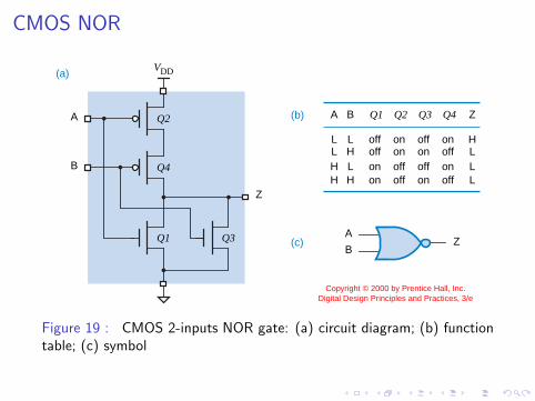
CMOS NOR
A
LLHH
B
LHLH
Q1
offoffonon
Q2
ononoffoff
Q3
offonoffon
Q4
onoffonoff
Z
HLLL
A
BZ
VDD
A
B
Z
Q2
Q4
Q1 Q3
(a)
(b)
(c)
Copyright © 2000 by Prentice Hall, Inc. Digital Design Principles and Practices, 3/e
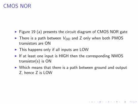
Figure 19 : CMOS 2-inputs NOR gate: (a) circuit diagram; (b) functiontable; (c) symbol
CMOS NOR
◮ Figure 19 (a) presents the circuit diagram of CMOS NOR gate
◮ There is a path between VDD and Z only when both PMOStransistors are ON
◮ This happens only if all inputs are LOW
◮ If at least one input is HIGH then the corresponding NMOStransistor(s) is ON
◮ Which means that there is a path between ground and outputZ, hence Z is LOW
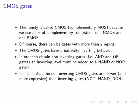
CMOS gates
◮ The family is called CMOS (complementary MOS) becausewe use pairs of complementary transistors: one NMOS andone PMOS
◮ Of course, there can be gates with more than 2 inputs
◮ The CMOS gates have a naturally inverting behaviour
◮ In order to obtain non-inverting gates (i.e. AND and ORgates) an inverting level must be added to a NAND or NORgate !
◮ It means that the non-inverting CMOS gates are slower (andmore expensive) than inverting gates (NOT, NAND, NOR)
Input-output transfer characteristic of a CMOS inverter
VIN
VOUT
undefinedLOW HIGH
0
1.5
3.5
5.0
0 1.5 3.5 5.0
HIGH
undefined
LOW
Copyright © 2000 by Prentice Hall, Inc. Digital Design Principles and Practices, 3/e
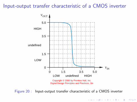
Figure 20 : Input-output transfer characteristic of a CMOS inverter
Outline
Principles and practice
Analog versus digital
Digital devices
Electronic aspects of digital devicesLogic levels, invalid levels and noise marginsLogic families: CMOS family
Integrated circuits
Digital-Design Levels
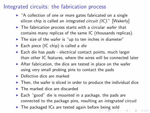
Integrated circuits: the fabrication process
◮ “A collection of one or more gates fabricated on a singlesilicon chip is called an integrated circuit (IC).” [Wakerly]
◮ The fabrication process starts with a circular wafer thatcontains many replicas of the same IC (thousands replicas).
◮ The size of the wafer is “up to ten inches in diameter”
◮ Each piece (IC chip) is called a die
◮ Each die has pads - electrical contact points, much largerthan other IC features, where the wires will be connected later
◮ After fabrication, the dice are tested in place on the waferusing very small probing pins to contact the pads
◮ Defective dice are marked
◮ Then, the wafer is sliced in order to produce the individual dice
◮ The marked dice are discarded
◮ Each “good” die is mounted in a package, the pads areconnected to the package pins, resulting an integrated circuit
◮ The packaged ICs are tested again before being sold

Integrated circuits: classification by size1. Small-Scale Integration (SSI):
◮ Contain the equivalent of 1 to 20 gates◮ Typically SSI ICs contain gates and flip-flops◮ They come in a 14-pin dual inline-pin (DIP) package (see
figure 21, (a))2. Medium-Scale Integration (MSI):
◮ Contain the equivalent of about 20 o 200 gates◮ Typically contain functional building blocks: decoders,
encoders, multiplexers, demultiplexer, registers, counters◮ The equivalent building blocks are used in larger ICs
3. Large-Scale Integration (LSI):◮ contain the equivalent of 200 to 1,000,000 gates or more◮ They include: small memories, microprocessors, programmable
logic devices, and customized devices4. Very Large-Scale Integration (VLSI):
◮ Separation between LSI and VLSI is fuzzy and is based ontransistor count
◮ ICs with a few millions of transistors are VLSI◮ They include most nowadays microprocessors and memories,
larger programmable logic devices and customized devices
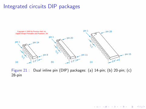
Integrated circuits DIP packages
(b) (c)(a) 0.3"
0.1"
pin 1 pin 14
pin 8
0.1"
pin 1 pin 20
0.3"
pin 11
0.6"
0.1"
pin 1 pin 28
pin 15
Copyright © 2000 by Prentice Hall, Inc. Digital Design Principles and Practices, 3/e
Figure 21 : Dual inline pin (DIP) packages: (a) 14-pin; (b) 20-pin; (c)28-pin
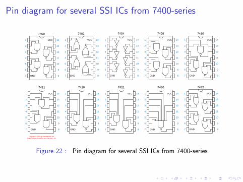
Pin diagram for several SSI ICs from 7400-series
1
2
3
4
5
6
7
14
13
12
11
10
9
8GND
VCC
7400
1
2
3
4
5
6
7
14
13
12
11
10
9
8GND
VCC
7402
1
2
3
4
5
6
7
14
13
12
11
10
9
8GND
VCC
7404
1
2
3
4
5
6
7
14
13
12
11
10
9
8GND
VCC
7410
1
2
3
4
5
6
7
14
13
12
11
10
9
8GND
VCC
7411
1
2
3
4
5
6
7
14
13
12
11
10
9
8GND
VCC
7420
1
2
3
4
5
6
7
14
13
12
11
10
9
8GND
VCC
7421
1
2
3
4
5
6
7
14
13
12
11
10
9
8GND
VCC
7430
1
2
3
4
5
6
7
14
13
12
11
10
9
8GND
VCC
7432
1
2
3
4
5
6
7
14
13
12
11
10
9
8GND
VCC
7408
Copyright © 2000 by Prentice Hall, Inc. Digital Design Principles and Practices, 3/e
Figure 22 : Pin diagram for several SSI ICs from 7400-series
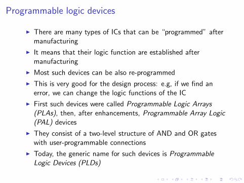
Programmable logic devices
◮ There are many types of ICs that can be “programmed” aftermanufacturing
◮ It means that their logic function are established aftermanufacturing
◮ Most such devices can be also re-programmed
◮ This is very good for the design process: e.g, if we find anerror, we can change the logic functions of the IC
◮ First such devices were called Programmable Logic Arrays(PLAs), then, after enhancements, Programmable Array Logic(PAL) devices
◮ They consist of a two-level structure of AND and OR gateswith user-programmable connections
◮ Today, the generic name for such devices is ProgrammableLogic Devices (PLDs)
Programmable logic devices
◮ There are technological limitations in the capacity increase ofPLDs.
◮ Two solutions have been developed:
1. Complex PLD (CPLD): a number of PLDs and aprogrammable structure that connects them (fig 23 (a))
2. Field Programmable Gate Arrays (FPGAs): a very largenumber of small individual logic blocks and a large, distributedinterconnection structure (fig 23 (b))
◮ Both CPLDs and FPGAs are used for prototyping and theyreduce the “time to market” of a product
◮ This is because of the use of HDLs (Hardware DescriptionLanguages) like VHDL or Verilog: a description of a devicerealized in a HDL can be synthesized and downloaded on aFPGA or CPLD chip in minutes.
◮ Synthesis is the process of transformation of a representationof a digital device to an equivalent lower level representation.
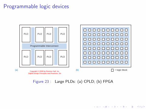
Programmable logic devices
PLD PLD PLD PLD
PLD PLD PLD PLD
Programmable Interconnect
(a) (b) = logic blockCopyright © 2000 by Prentice Hall, Inc.
Digital Design Principles and Practices, 3/e
Figure 23 : Large PLDs: (a) CPLD; (b) FPGA
Application-Specific ICs
◮ The costs of a LSI chip entirely designed for a specificcustomer (from chip’s functions to the transistor level) areextremely high (more than 500,000 USD), being efficient onlyfor mass production (e.g. microprocessors, buss-interface chip)
◮ In order to reduce the costs per chip, semicustom ICs, orapplication-specific ICs (ASICs) have been developed
◮ ASICs are “chips designed for a particular, limited product orapplication”
◮ IC manufacturers have developed libraries of standard cells,which usually contain MSI common functions like decoders,registers, counters, or LSI functions like memories
◮ The ASICS rely on standard cell design: the logic designerinterconnects such functions using the libraries of standardcells

Printed-Circuit Boards
◮ ICs are mounted on printed-circuit boards (PCBs), called alsoprinted-wired boards PWBs
◮ A multilayer PCB “have copper wiring etched on multiple,thin layers of fiberglass that are laminated into a single board”
◮ Individual wire connections are called PCB traces
◮ Most modern PCBs use surface-mount technology (SMT)
◮ The ICs are called SMDs (surface-mounted devices)
◮ They are mounted on PCB (usually by machine), with theirleads bent, and held in place by a solder paste
◮ Then the entire PCB is passed through an oven to melt thesolder paste
◮ Old DIP chips have long pins that poke through the boardand are soldered on the underside
Outline
Principles and practice
Analog versus digital
Digital devices
Electronic aspects of digital devicesLogic levels, invalid levels and noise marginsLogic families: CMOS family
Integrated circuits
Digital-Design Levels
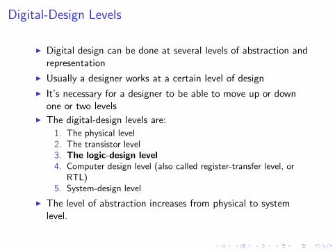
Digital-Design Levels
◮ Digital design can be done at several levels of abstraction andrepresentation
◮ Usually a designer works at a certain level of design
◮ It’s necessary for a designer to be able to move up or downone or two levels
◮ The digital-design levels are:
1. The physical level2. The transistor level3. The logic-design level
4. Computer design level (also called register-transfer level, orRTL)
5. System-design level
◮ The level of abstraction increases from physical to systemlevel.
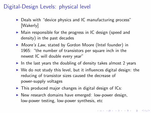
Digital-Design Levels: physical level
◮ Deals with “device physics and IC manufacturing process”[Wakerly]
◮ Main responsible for the progress in IC design (speed anddensity) in the past decades
◮ Moore’s Law, stated by Gordon Moore (Intel founder) in1965: “the number of transistors per square inch in thenewest IC will double every year”
◮ In the last years the doubling of density takes almost 2 years
◮ We do not study this level, but it influences digital design: thereducing of transistor sizes caused the decrease ofpower-supply voltages
◮ This produced major changes in digital design of ICs:
◮ New research domains have emerged: low-power design,low-power testing, low-power synthesis, etc
Digital-Design Levels
◮ Transistor level◮ It is not the subject of the Digital Logic course◮ It will be the main topics of the Integrated Circuits course
◮ Logic-design level◮ It is the level of Digital Logic course◮ We will learn how to synthesize RTL devices (multiplexers,
demultiplexers, decoders, counters, registers, etc) from gatesand flip-flops
◮ Computer design level, or Register-transfer level (RTL):◮ Courses: Computer Architecture, Computer Organization,
Microprocessors◮ You will use what you learn at the Digital Logic course
◮ System-design level◮ Courses: Operating systems, Compilers, etc
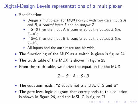
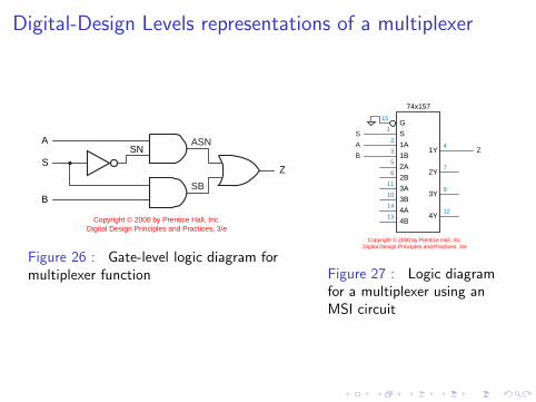
Digital-Design Levels representations of a multiplexer
◮ Specification:◮ Design a multiplexer (or MUX) circuit with two data inputs A
and B, a control input S and an output Z◮ If S=0 then the input A is transferred at the output Z (i.e.
Z=A);◮ If S=1 then the input B is transferred at the output Z (i.e.
Z=B);◮ All inputs and the output are one bit wide
◮ The functioning of the MUX as a switch is given is figure 24
◮ The truth table of the MUX is shown in figure 25
◮ From the truth table, we derive the equation for the MUX:
Z = S ′· A+ S · B
◮ The equation reads: “Z equals not S and A, or S and B”
◮ The gate-level logic diagram that corresponds to this equationis shown in figure 26, and the MSI IC in figure 27

Digital-Design Levels representations of a multiplexer
A
B
Z
S
Copyright © 2000 by Prentice Hall, Inc. Digital Design Principles and Practices, 3/e
Figure 24 : Switch model formultiplexer function
Table 1 -1Truth table for the multiplexer function.
S A B Z
0 0 0 0
0 0 1 0
0 1 0 1
0 1 1 1
1 0 0 0
1 0 1 1
1 1 0 0
1 1 1 1
Figure 25 : Truth table formultiplexer function
Digital-Design Levels representations of a multiplexer
A
S
B
Z
SNASN
SB
Copyright © 2000 by Prentice Hall, Inc. Digital Design Principles and Practices, 3/e
Figure 26 : Gate-level logic diagram formultiplexer function
74x157
1A
1B
2A
2B
3A
3B
4A
4B
G
24
1Y
72Y
93Y
124Y
3
5
6
11
10
14
13
S1
15
S
B
AZ
Copyright © 2000 by Prentice Hall, Inc. Digital Design Principles and Practices, 3/e
Figure 27 : Logic diagramfor a multiplexer using anMSI circuit