Embed Size (px)
Citation preview
Introduction toCMOS VLSI
Design
Lecture 1: Circuits & Layout
David Harris
Harvey Mudd CollegeSpring 2004
1: Circuits & Layout Slide 2CMOS VLSI Design
Outlineq A Brief Historyq CMOS Gate Designq Pass Transistorsq CMOS Latches & Flip-Flopsq Standard Cell Layoutsq Stick Diagrams
1: Circuits & Layout Slide 3CMOS VLSI Design
A Brief Historyq 1958: First integrated circuit
– Flip-flop using two transistors– Built by Jack Kilby at Texas Instruments
q 2003– Intel Pentium 4 µprocessor (55 million transistors)– 512 Mbit DRAM (> 0.5 billion transistors)
q 53% compound annual growth rate over 45 years– No other technology has grown so fast so long
q Driven by miniaturization of transistors– Smaller is cheaper, faster, lower in power!– Revolutionary effects on society

1: Circuits & Layout Slide 4CMOS VLSI Design
Annual Salesq 1018 transistors manufactured in 2003
– 100 million for every human on the planet
0
50
100
150
200
1982 1984 1986 1988 1990 1992 1994 1996 1998 2000 2002
Year
Global S
emiconductor B
illings(B
illions of US
$)
1: Circuits & Layout Slide 5CMOS VLSI Design
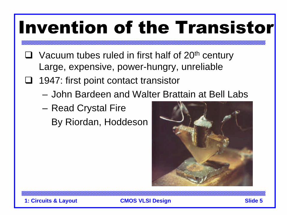
Invention of the Transistorq Vacuum tubes ruled in first half of 20th century
Large, expensive, power-hungry, unreliableq 1947: first point contact transistor
– John Bardeen and Walter Brattain at Bell Labs– Read Crystal Fire
By Riordan, Hoddeson
1: Circuits & Layout Slide 6CMOS VLSI Design
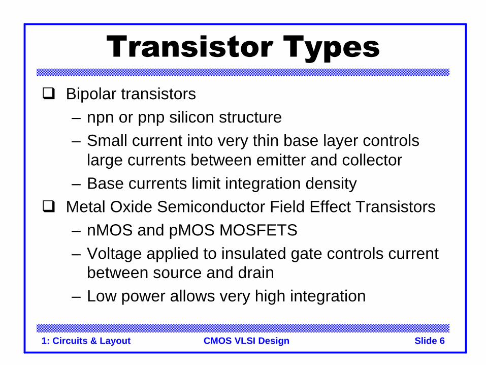
Transistor Typesq Bipolar transistors
– npn or pnp silicon structure– Small current into very thin base layer controls
large currents between emitter and collector– Base currents limit integration density
q Metal Oxide Semiconductor Field Effect Transistors– nMOS and pMOS MOSFETS– Voltage applied to insulated gate controls current
between source and drain– Low power allows very high integration
1: Circuits & Layout Slide 7CMOS VLSI Design
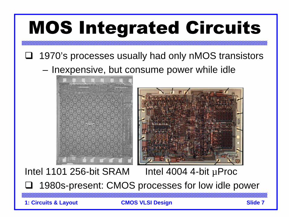
MOS Integrated Circuitsq 1970’s processes usually had only nMOS transistors
– Inexpensive, but consume power while idle
q 1980s-present: CMOS processes for low idle powerIntel 1101 256-bit SRAM Intel 4004 4-bit µProc
1: Circuits & Layout Slide 8CMOS VLSI Design
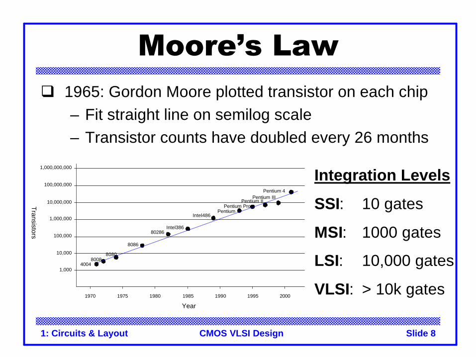
Moore’s Lawq 1965: Gordon Moore plotted transistor on each chip
– Fit straight line on semilog scale– Transistor counts have doubled every 26 months
Year
Transistors
40048008
8080
8086
80286Intel386
Intel486Pentium
Pentium ProPentium II
Pentium IIIPentium 4
1,000
10,000
100,000
1,000,000
10,000,000
100,000,000
1,000,000,000
1970 1975 1980 1985 1990 1995 2000
Integration Levels
SSI: 10 gates
MSI: 1000 gates
LSI: 10,000 gates
VLSI: > 10k gates
1: Circuits & Layout Slide 9CMOS VLSI Design
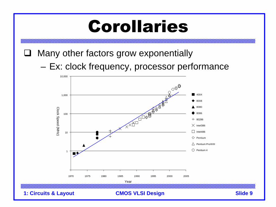
Corollariesq Many other factors grow exponentially
– Ex: clock frequency, processor performance
Year
1
10
100
1,000
10,000
1970 1975 1980 1985 1990 1995 2000 2005
4004
8008
8080
8086
80286
Intel386
Intel486
Pentium
Pentium Pro/II/III
Pentium 4
Clock S
peed (MH
z)
1: Circuits & Layout Slide 10CMOS VLSI Design
CMOS Gate Designq Activity:
– Sketch a 4-input CMOS NAND gate
1: Circuits & Layout Slide 11CMOS VLSI Design
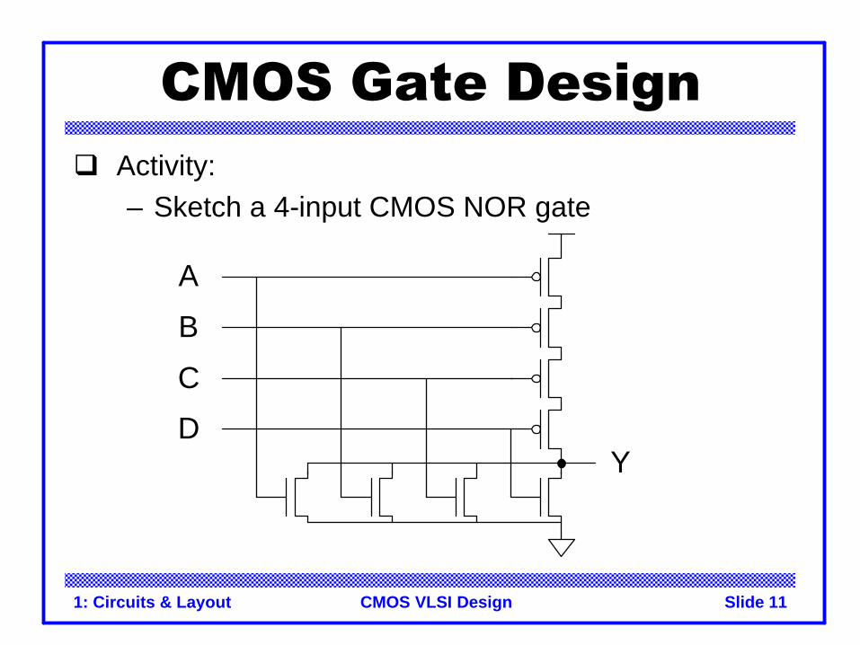
CMOS Gate Designq Activity:
– Sketch a 4-input CMOS NOR gate
A
B
C
DY
1: Circuits & Layout Slide 12CMOS VLSI Design
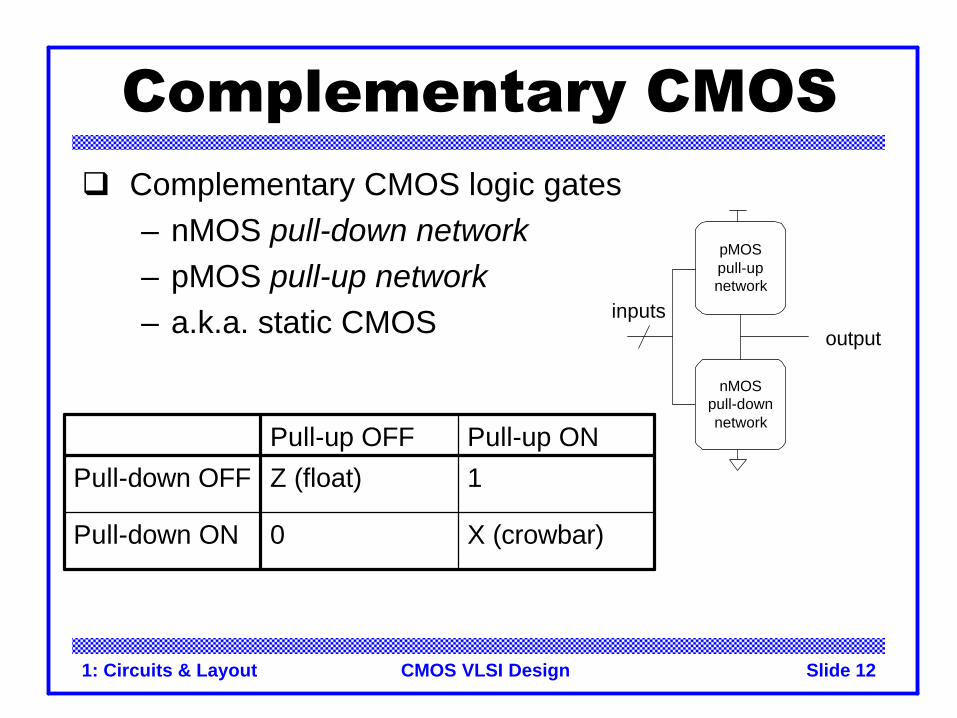
Complementary CMOSq Complementary CMOS logic gates
– nMOS pull-down network– pMOS pull-up network– a.k.a. static CMOS
pMOSpull-upnetwork
outputinputs
nMOSpull-downnetwork
X (crowbar)0Pull-down ON
1Z (float)Pull-down OFF
Pull-up ONPull-up OFF
1: Circuits & Layout Slide 13CMOS VLSI Design
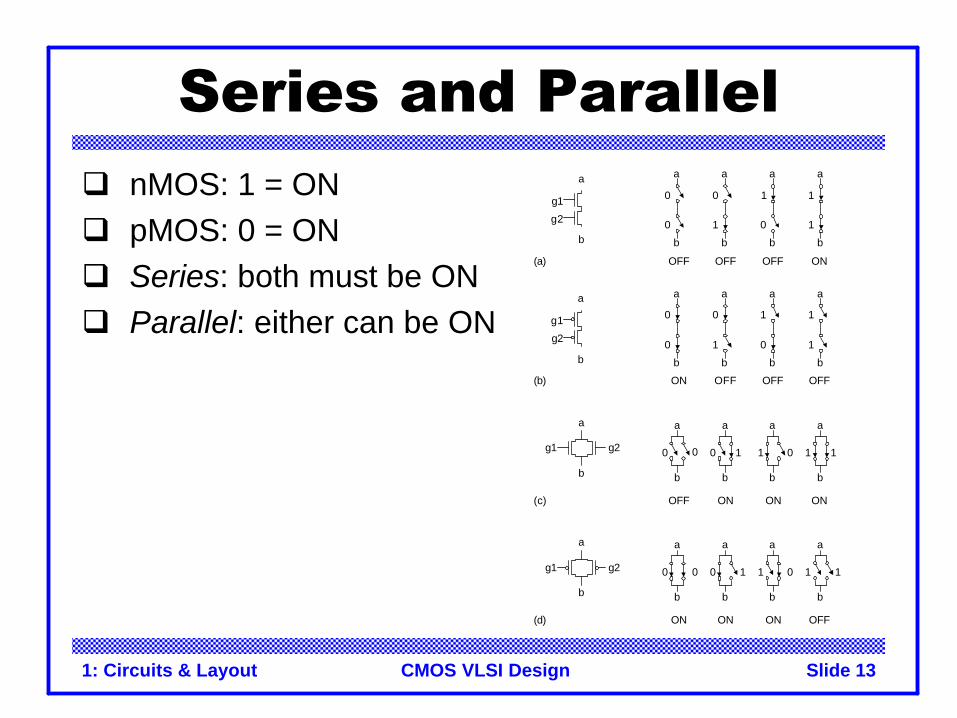
Series and Parallelq nMOS: 1 = ONq pMOS: 0 = ONq Series: both must be ONq Parallel: either can be ON
(a)
a
b
a
b
g1
g2
0
0
a
b
0
1
a
b
1
0
a
b
1
1
OFF OFF OFF ON
(b)
a
b
a
b
g1
g2
0
0
a
b
0
1
a
b
1
0
a
b
1
1
ON OFF OFF OFF
(c)
a
b
a
b
g1 g2 0 0
OFF ON ON ON
(d) ON ON ON OFF
a
b
0
a
b
1
a
b
11 0 1
a
b
0 0
a
b
0
a
b
1
a
b
11 0 1
a
b
g1 g2
1: Circuits & Layout Slide 14CMOS VLSI Design
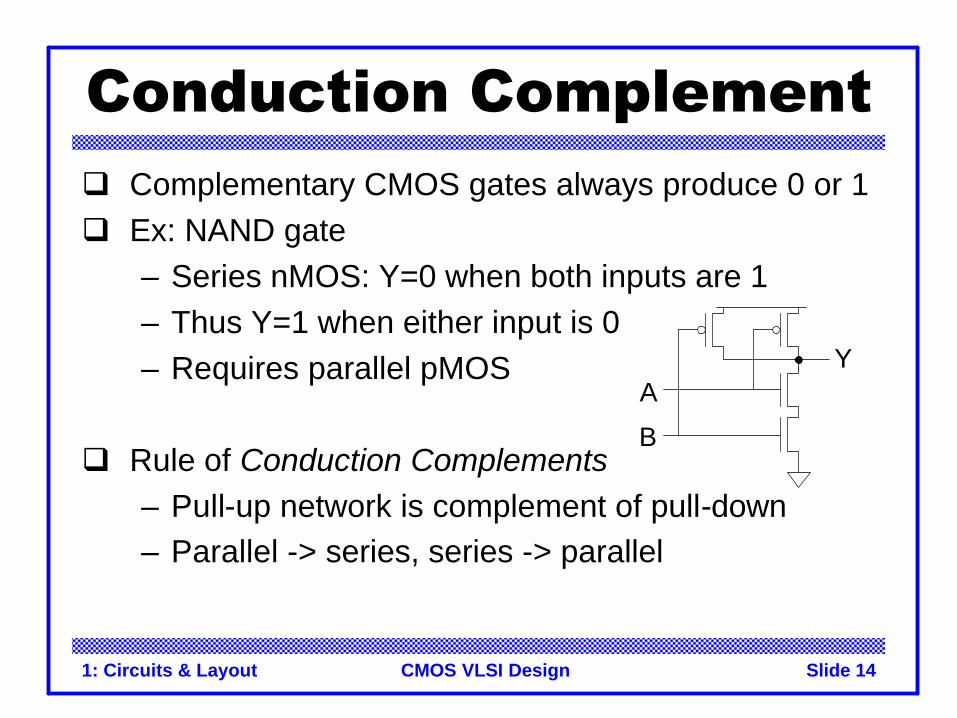
Conduction Complementq Complementary CMOS gates always produce 0 or 1q Ex: NAND gate
– Series nMOS: Y=0 when both inputs are 1– Thus Y=1 when either input is 0– Requires parallel pMOS
q Rule of Conduction Complements– Pull-up network is complement of pull-down– Parallel -> series, series -> parallel
A
B
Y
1: Circuits & Layout Slide 15CMOS VLSI Design
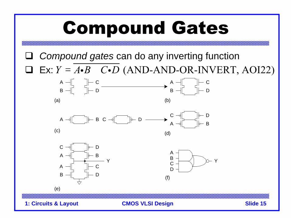
Compound Gatesq Compound gates can do any inverting functionq Ex: (AND-AND-OR-INVERT, AOI22)Y A B C D= +i i
A
B
C
D
A
B
C
D
A B C DA B
C D
B
D
YA
CA
C
A
B
C
D
B
D
Y
(a)
(c)
(e)
(b)
(d)
(f)
1: Circuits & Layout Slide 16CMOS VLSI Design
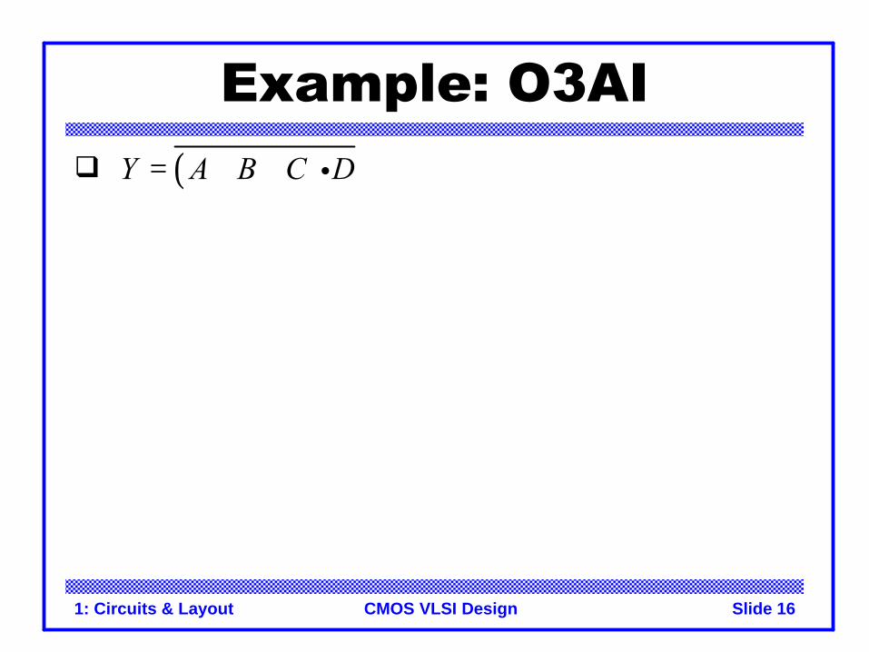
Example: O3AIq ( )Y A B C D= + + i
1: Circuits & Layout Slide 17CMOS VLSI Design
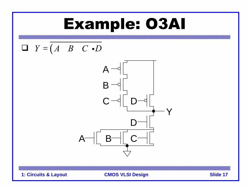
Example: O3AI q ( )Y A B C D= + + i
A B
Y
C
D
DC
B
A
1: Circuits & Layout Slide 18CMOS VLSI Design
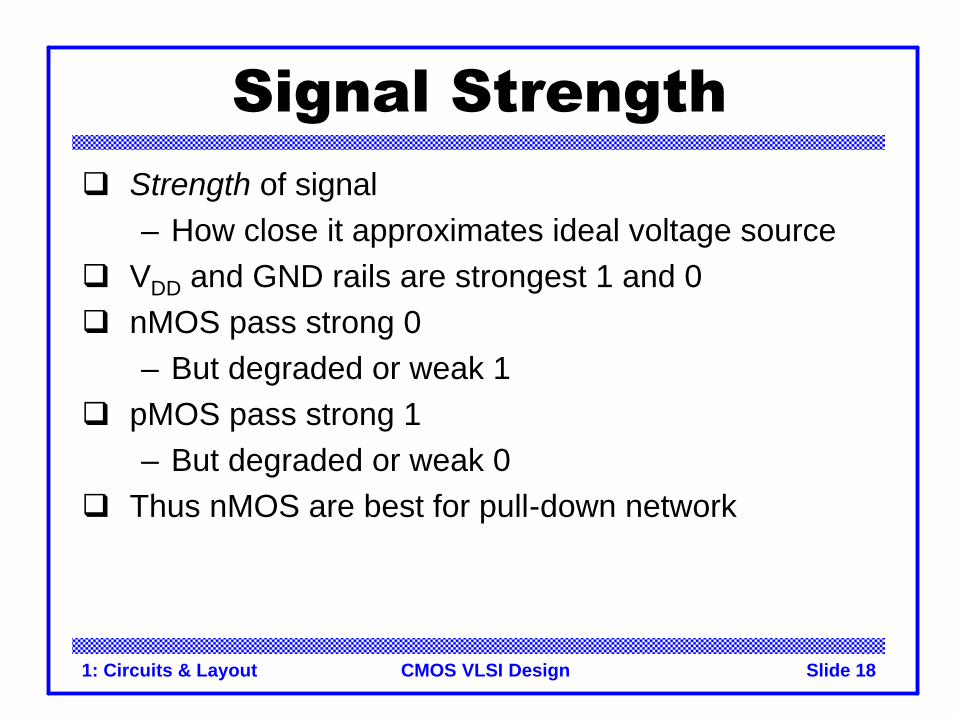
Signal Strengthq Strength of signal
– How close it approximates ideal voltage sourceq VDD and GND rails are strongest 1 and 0q nMOS pass strong 0
– But degraded or weak 1q pMOS pass strong 1
– But degraded or weak 0q Thus nMOS are best for pull-down network
1: Circuits & Layout Slide 19CMOS VLSI Design
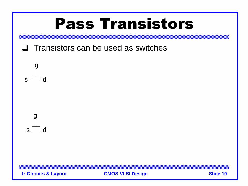
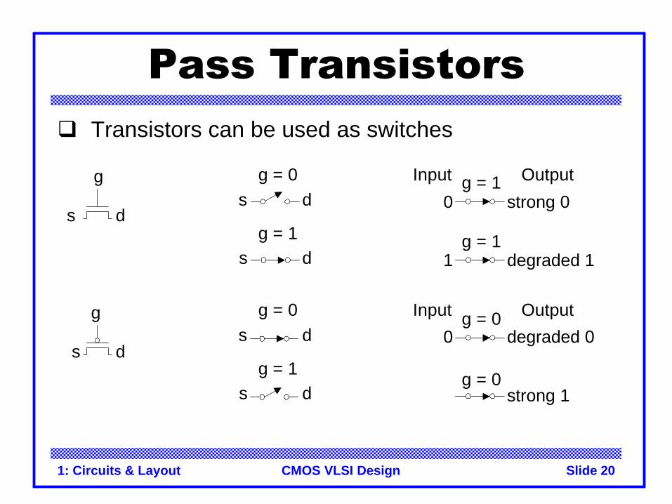
Pass Transistorsq Transistors can be used as switches
g
s d
g
s d
1: Circuits & Layout Slide 20CMOS VLSI Design
Pass Transistorsq Transistors can be used as switches
g
s d
g = 0s d
g = 1s d
0 strong 0
Input Output
1 degraded 1
g
s d
g = 0s d
g = 1s d
0 degraded 0
Input Output
strong 1
g = 1
g = 1
g = 0
g = 0
1: Circuits & Layout Slide 21CMOS VLSI Design
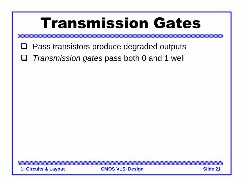
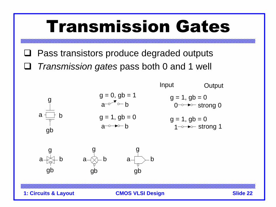
Transmission Gatesq Pass transistors produce degraded outputsq Transmission gates pass both 0 and 1 well
1: Circuits & Layout Slide 22CMOS VLSI Design
Transmission Gatesq Pass transistors produce degraded outputsq Transmission gates pass both 0 and 1 well
g = 0, gb = 1a b
g = 1, gb = 0a b
0 strong 0
Input Output
1 strong 1
g
gb
a b
a bg
gb
a b
g
gb
a b
g
gb
g = 1, gb = 0
g = 1, gb = 0
1: Circuits & Layout Slide 23CMOS VLSI Design
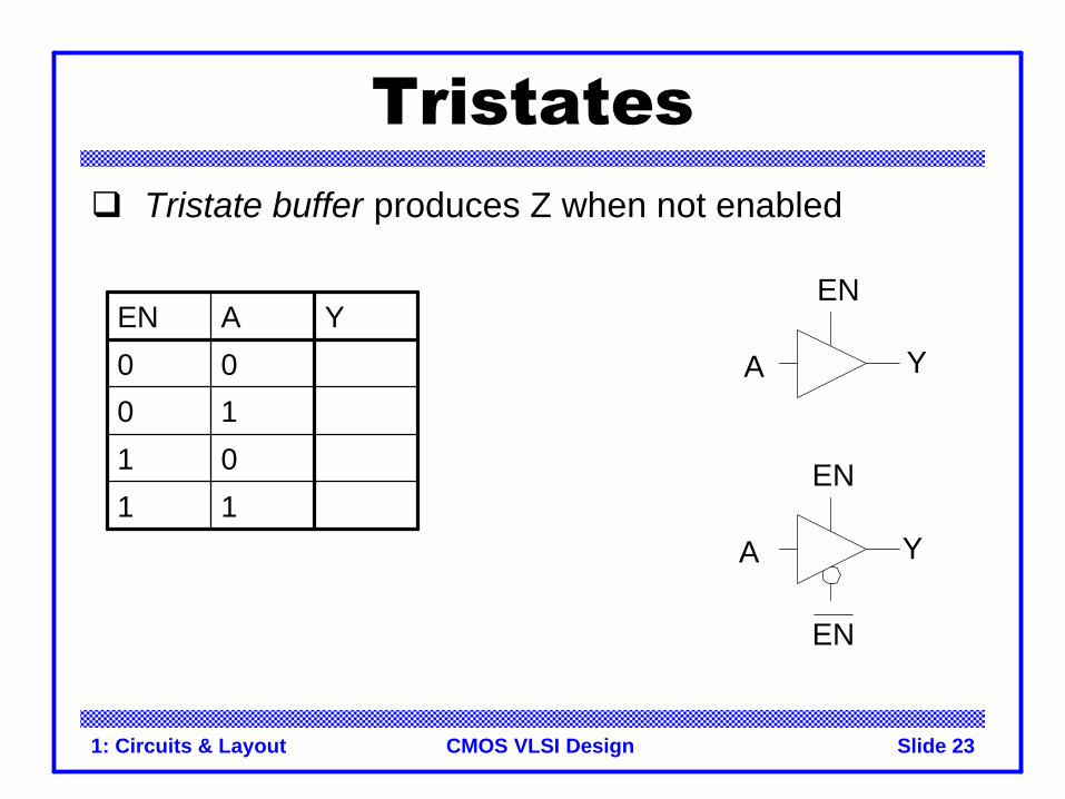
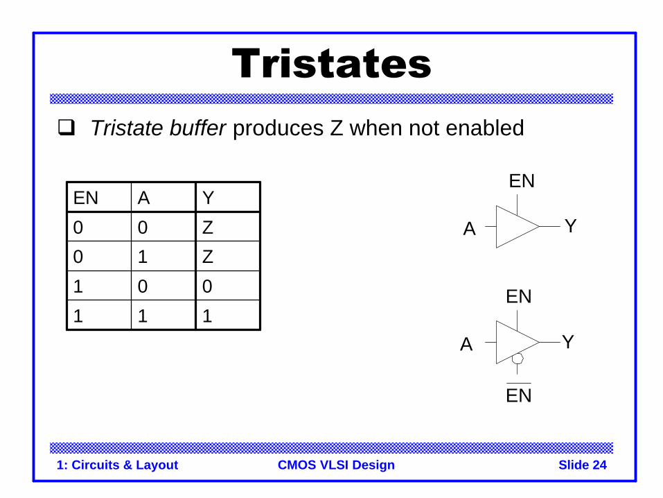
Tristatesq Tristate buffer produces Z when not enabled
11
01
10
00
YAEN
A Y
EN
A Y
EN
EN
1: Circuits & Layout Slide 24CMOS VLSI Design
Tristatesq Tristate buffer produces Z when not enabled
111
001
Z10
Z00
YAEN
A Y
EN
A Y
EN
EN
1: Circuits & Layout Slide 25CMOS VLSI Design
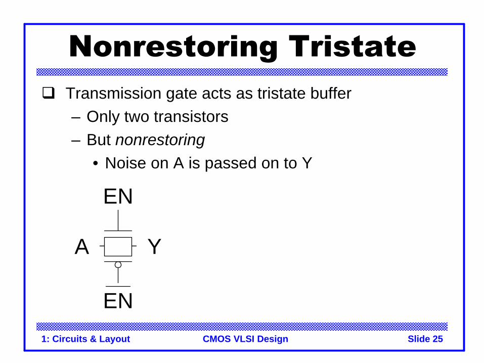
Nonrestoring Tristateq Transmission gate acts as tristate buffer
– Only two transistors– But nonrestoring
• Noise on A is passed on to Y
A Y
EN
EN
1: Circuits & Layout Slide 26CMOS VLSI Design
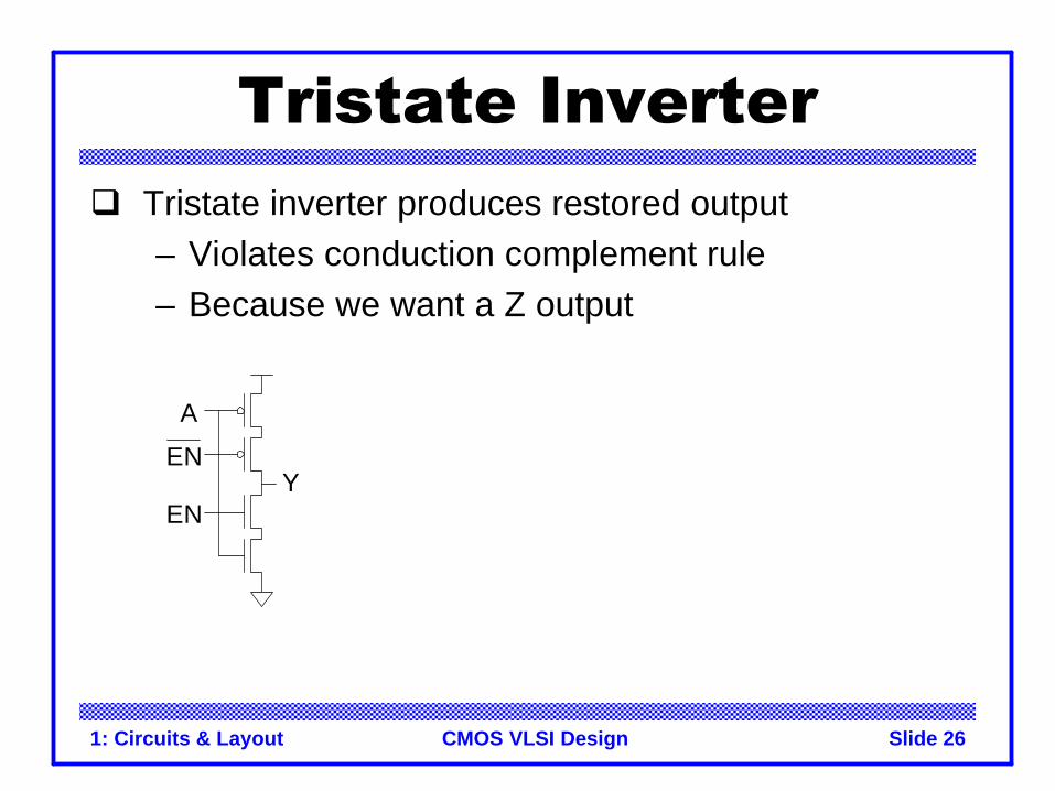
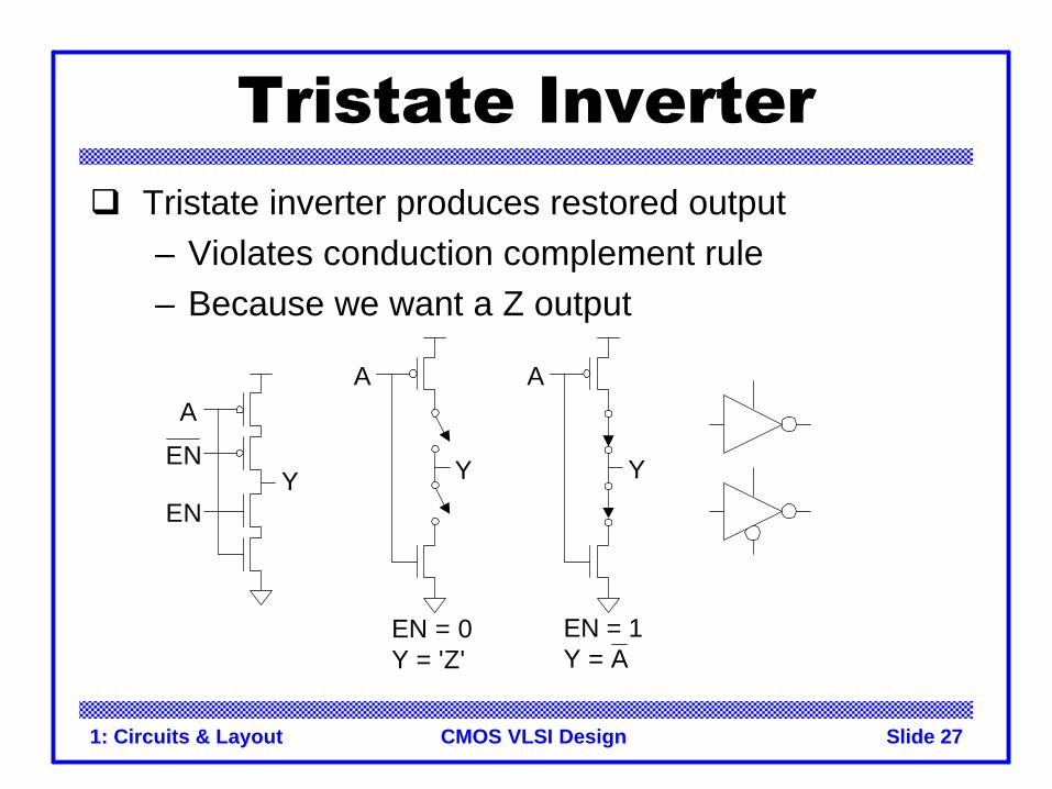
Tristate Inverterq Tristate inverter produces restored output
– Violates conduction complement rule– Because we want a Z output
A
YEN
EN
1: Circuits & Layout Slide 27CMOS VLSI Design
Tristate Inverterq Tristate inverter produces restored output
– Violates conduction complement rule– Because we want a Z output
A
YEN
A
Y
EN = 0Y = 'Z'
Y
EN = 1Y = A
A
EN
1: Circuits & Layout Slide 28CMOS VLSI Design
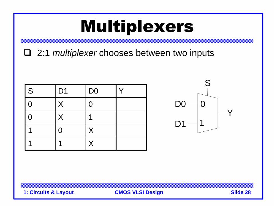
Multiplexersq 2:1 multiplexer chooses between two inputs
X11
X01
1X0
0X0
YD0D1S
0
1
S
D0
D1Y
1: Circuits & Layout Slide 29CMOS VLSI Design
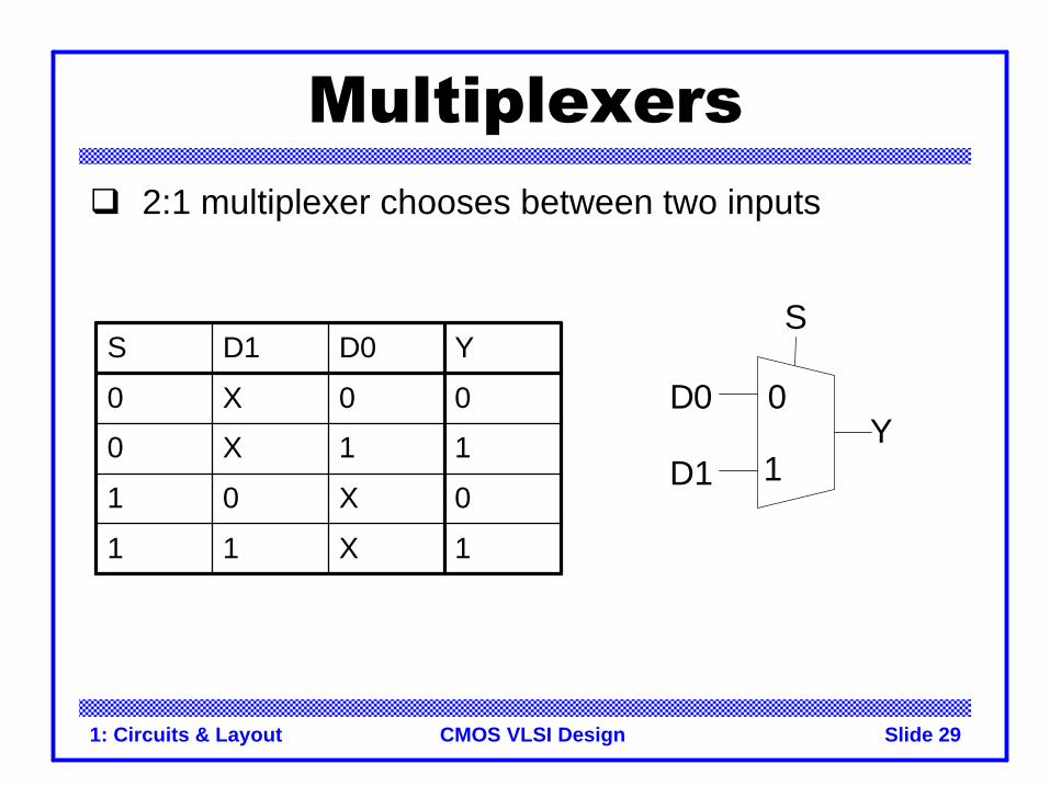
Multiplexersq 2:1 multiplexer chooses between two inputs
1X11
0X01
11X0
00X0
YD0D1S
0
1
S
D0
D1Y
1: Circuits & Layout Slide 30CMOS VLSI Design
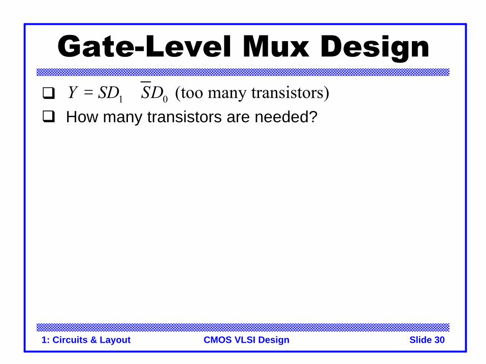
Gate-Level Mux Designqq How many transistors are needed?
1 0 (too many transistors)Y SD SD= +
1: Circuits & Layout Slide 31CMOS VLSI Design
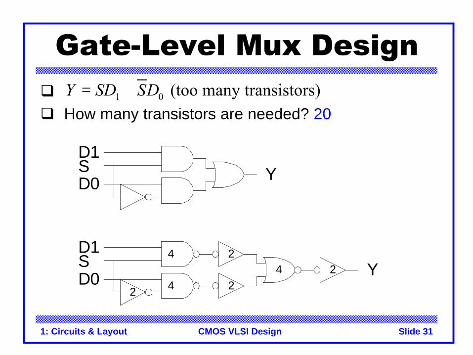
Gate-Level Mux Designqq How many transistors are needed? 20
1 0 (too many transistors)Y SD SD= +
44
D1
D0S Y
4
2
22 Y
2
D1
D0S
1: Circuits & Layout Slide 32CMOS VLSI Design
Transmission Gate Muxq Nonrestoring mux uses two transmission gates
1: Circuits & Layout Slide 33CMOS VLSI Design
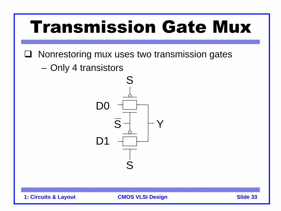
Transmission Gate Muxq Nonrestoring mux uses two transmission gates
– Only 4 transistorsS
S
D0
D1
YS
1: Circuits & Layout Slide 34CMOS VLSI Design
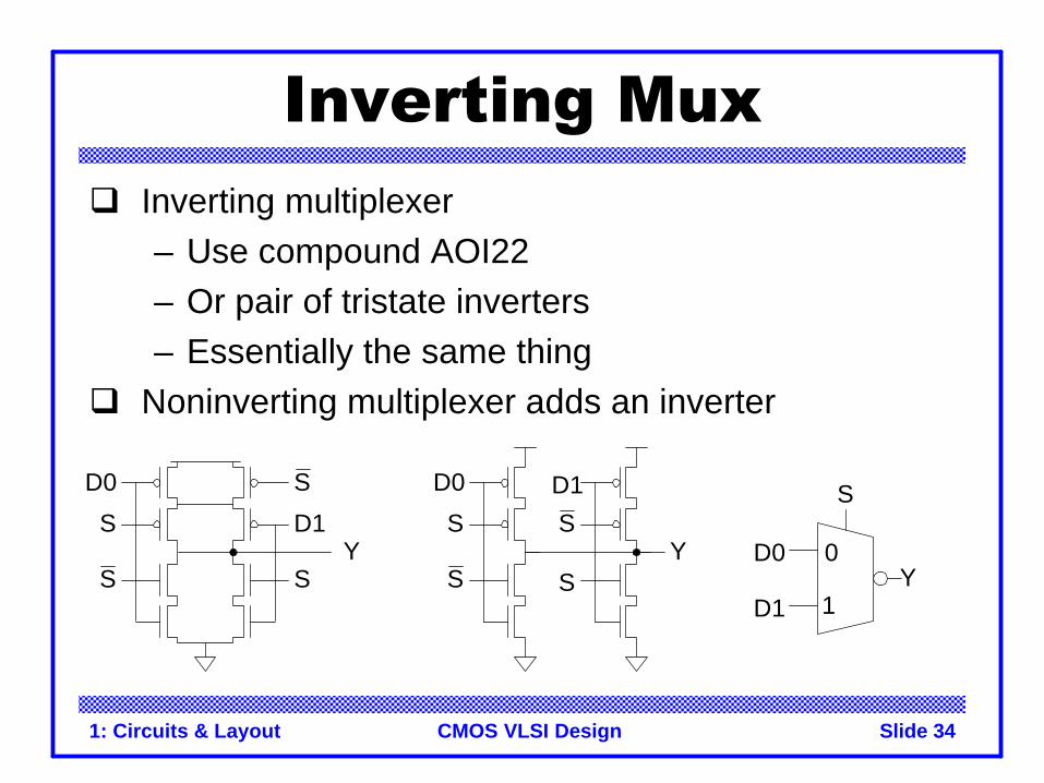
Inverting Muxq Inverting multiplexer
– Use compound AOI22– Or pair of tristate inverters– Essentially the same thing
q Noninverting multiplexer adds an inverter
S
D0 D1
Y
S
D0
D1Y
0
1S
Y
D0
D1
S
S
S
S
S
S
1: Circuits & Layout Slide 35CMOS VLSI Design
4:1 Multiplexerq 4:1 mux chooses one of 4 inputs using two selects
1: Circuits & Layout Slide 36CMOS VLSI Design
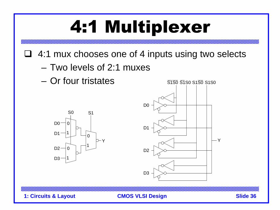
4:1 Multiplexerq 4:1 mux chooses one of 4 inputs using two selects
– Two levels of 2:1 muxes– Or four tristates
S0
D0
D1
0
1
0
1
0
1Y
S1
D2
D3
D0
D1
D2
D3
Y
S1S0 S1S0 S1S0 S1S0
1: Circuits & Layout Slide 37CMOS VLSI Design
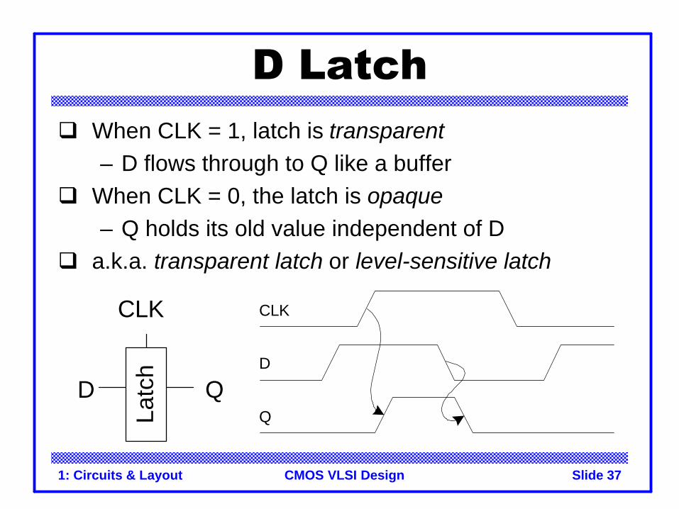
D Latchq When CLK = 1, latch is transparent
– D flows through to Q like a bufferq When CLK = 0, the latch is opaque
– Q holds its old value independent of Dq a.k.a. transparent latch or level-sensitive latch
CLK
D Q
Latc
h D
CLK
Q
1: Circuits & Layout Slide 38CMOS VLSI Design
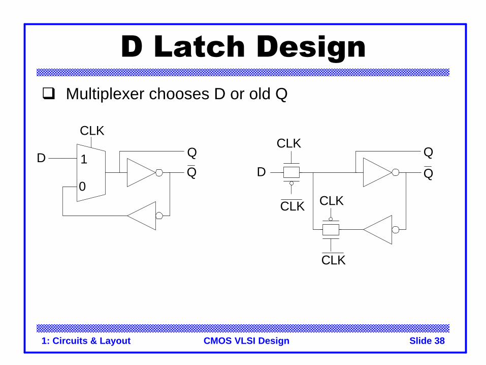
D Latch Designq Multiplexer chooses D or old Q
1
0
D
CLK
QCLK
CLKCLK
CLK
DQ Q
Q
1: Circuits & Layout Slide 39CMOS VLSI Design
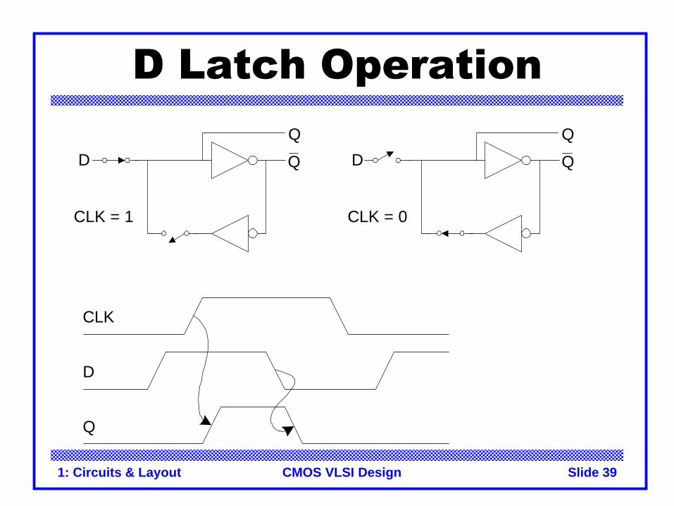
D Latch Operation
CLK = 1
D Q
Q
CLK = 0
D Q
Q
D
CLK
Q
1: Circuits & Layout Slide 40CMOS VLSI Design
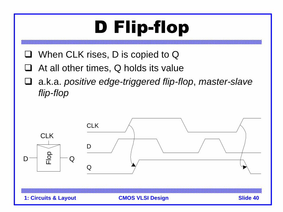
D Flip-flopq When CLK rises, D is copied to Qq At all other times, Q holds its valueq a.k.a. positive edge-triggered flip-flop, master-slave
flip-flop
Flo
p
CLK
D Q
D
CLK
Q
1: Circuits & Layout Slide 41CMOS VLSI Design
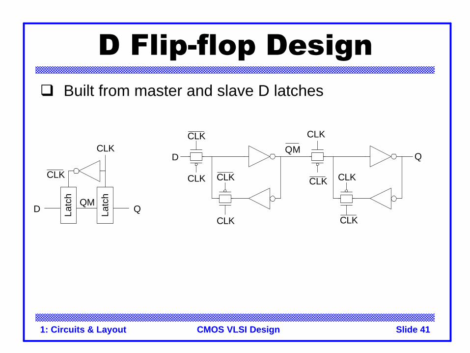
D Flip-flop Designq Built from master and slave D latches
QM
CLK
CLKCLK
CLK
Q
CLK
CLK
CLK
CLK
D
Latc
h
Latc
h
D QQM
CLK
CLK
1: Circuits & Layout Slide 42CMOS VLSI Design
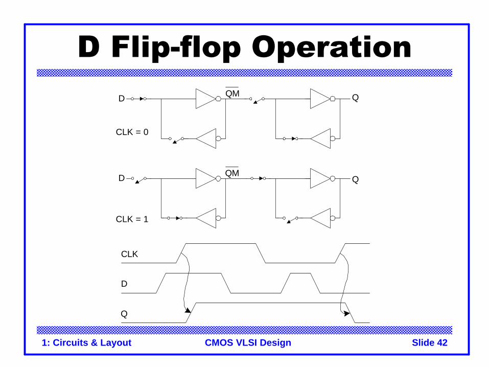
D Flip-flop Operation
CLK = 1
D
CLK = 0
Q
D
QM
QMQ
D
CLK
Q
1: Circuits & Layout Slide 43CMOS VLSI Design
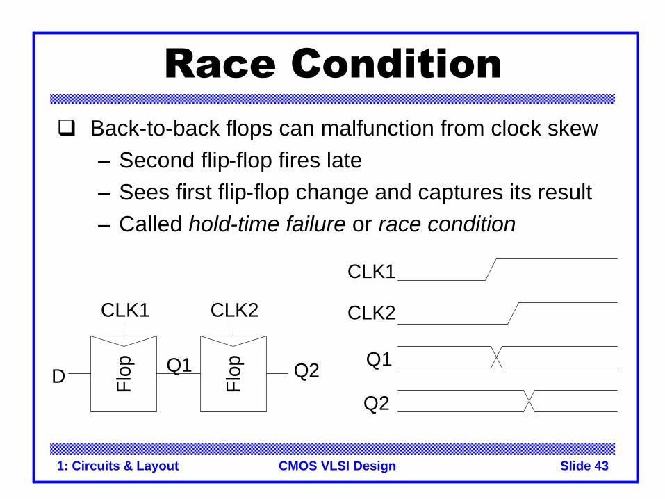
Race Conditionq Back-to-back flops can malfunction from clock skew
– Second flip-flop fires late– Sees first flip-flop change and captures its result– Called hold-time failure or race condition
CLK1
D Q1
Flop
Flop
CLK2
Q2
CLK1
CLK2
Q1
Q2
1: Circuits & Layout Slide 44CMOS VLSI Design
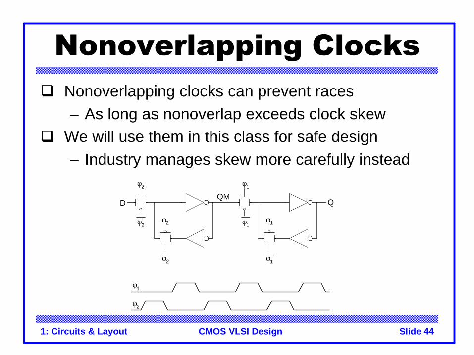
Nonoverlapping Clocksq Nonoverlapping clocks can prevent races
– As long as nonoverlap exceeds clock skewq We will use them in this class for safe design
– Industry manages skew more carefully instead φ1
φ1φ1
φ1
φ2
φ2φ2
φ2
φ2
φ1
QMQD
1: Circuits & Layout Slide 45CMOS VLSI Design
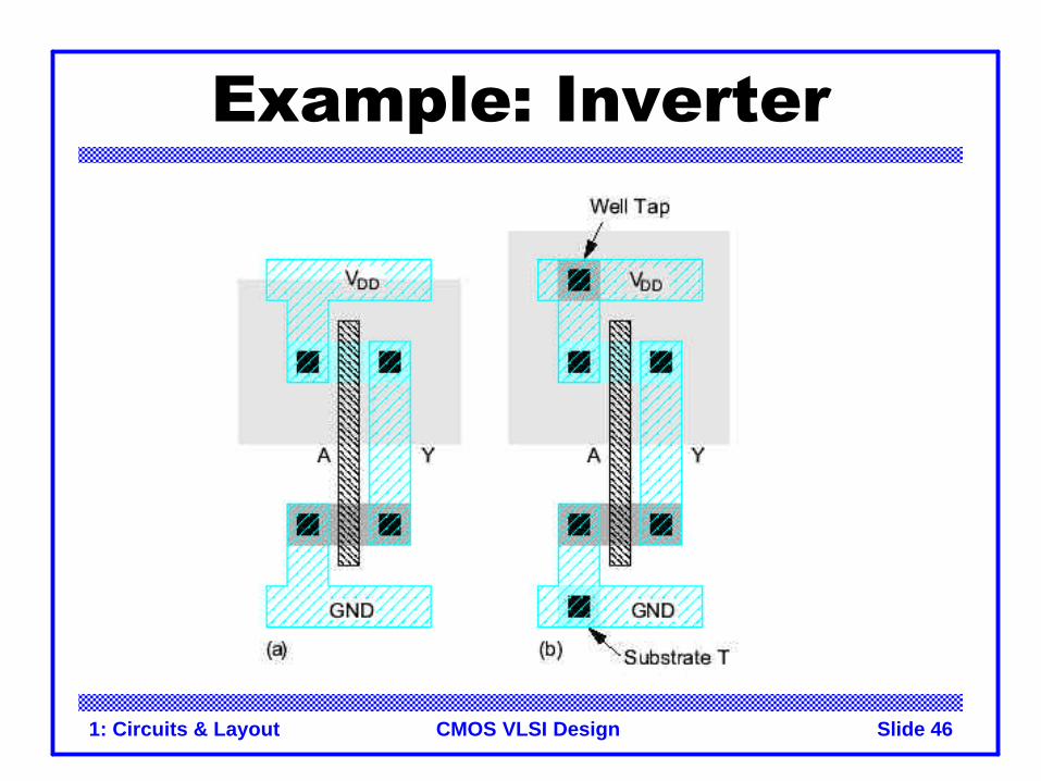
Gate Layoutq Layout can be very time consuming
– Design gates to fit together nicely– Build a library of standard cells
q Standard cell design methodology– VDD and GND should abut (standard height)– Adjacent gates should satisfy design rules– nMOS at bottom and pMOS at top– All gates include well and substrate contacts
1: Circuits & Layout Slide 46CMOS VLSI Design
Example: Inverter
1: Circuits & Layout Slide 47CMOS VLSI Design
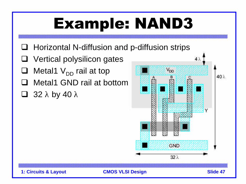
Example: NAND3q Horizontal N-diffusion and p-diffusion stripsq Vertical polysilicon gatesq Metal1 VDD rail at topq Metal1 GND rail at bottomq 32 λ by 40 λ
1: Circuits & Layout Slide 48CMOS VLSI Design
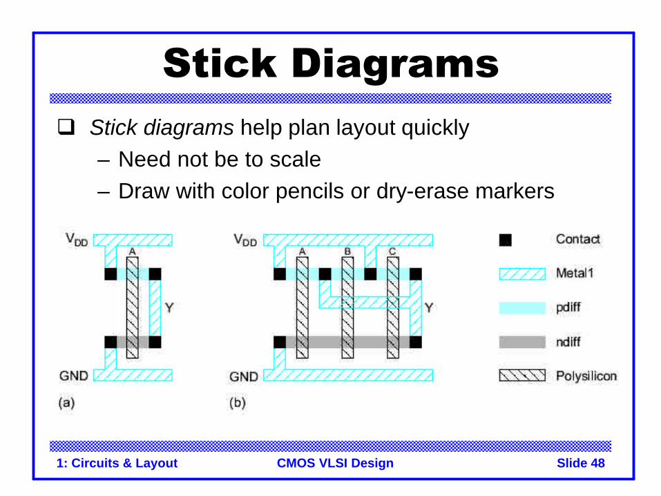
Stick Diagramsq Stick diagrams help plan layout quickly
– Need not be to scale– Draw with color pencils or dry-erase markers
1: Circuits & Layout Slide 49CMOS VLSI Design
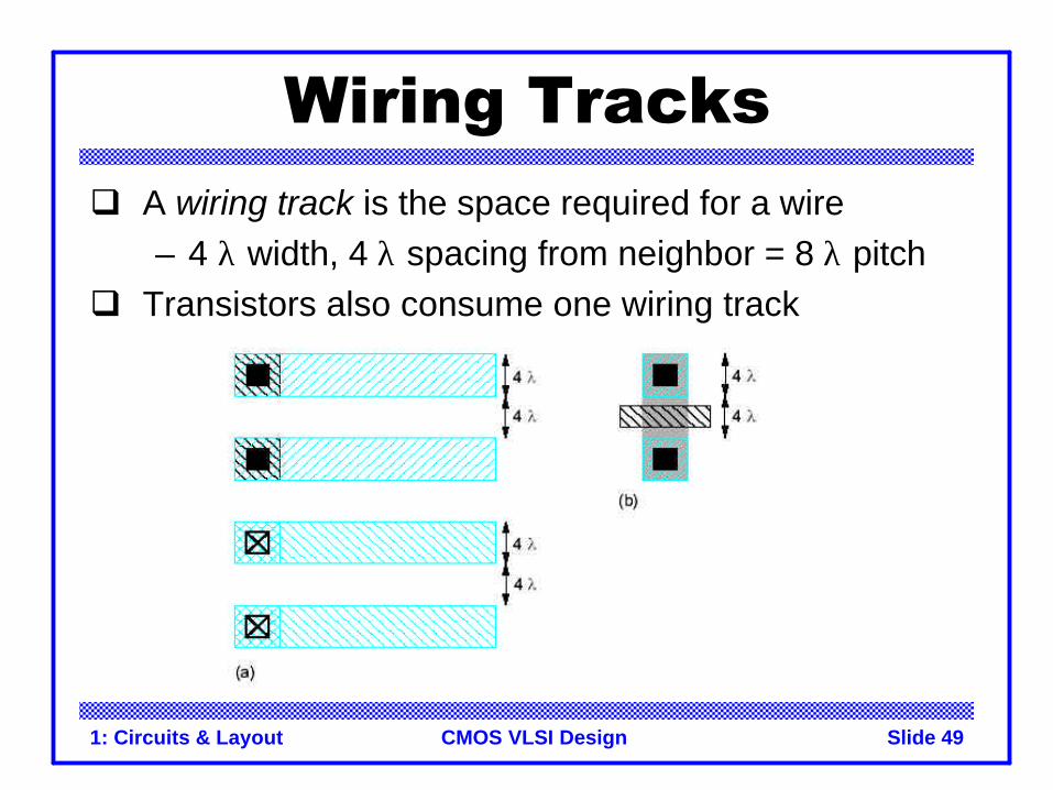
Wiring Tracksq A wiring track is the space required for a wire
– 4 λ width, 4 λ spacing from neighbor = 8 λ pitchq Transistors also consume one wiring track
1: Circuits & Layout Slide 50CMOS VLSI Design
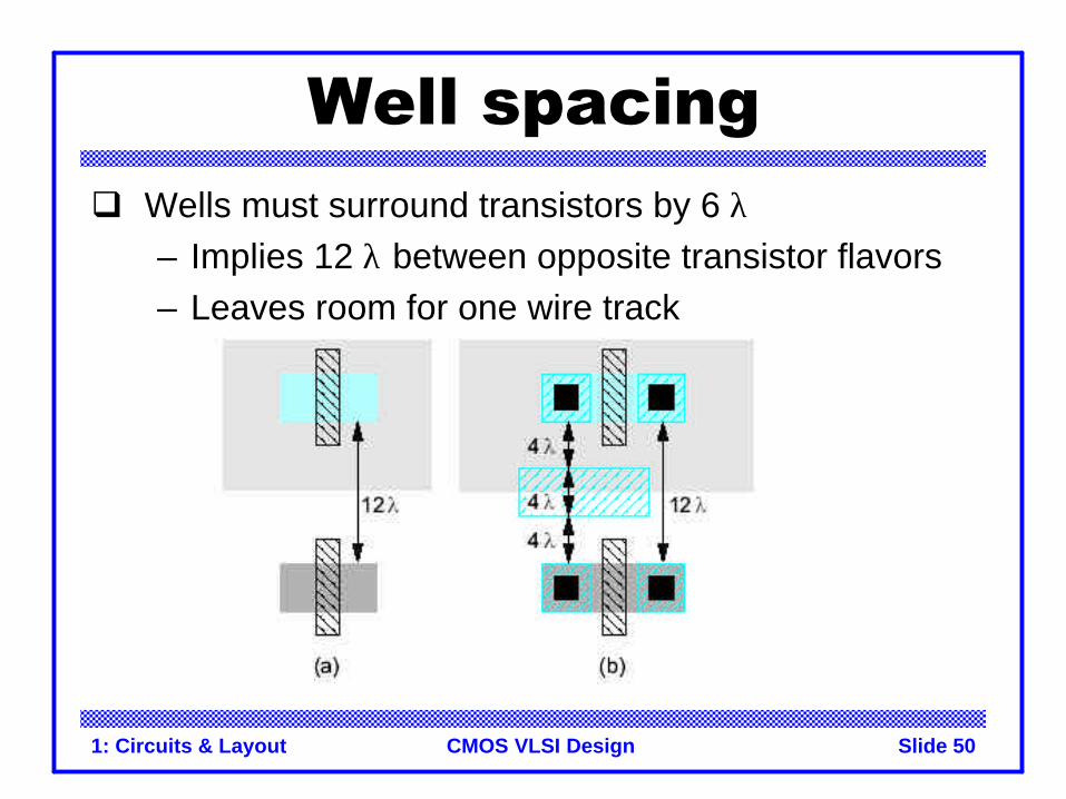
Well spacingq Wells must surround transistors by 6 λ
– Implies 12 λ between opposite transistor flavors– Leaves room for one wire track
1: Circuits & Layout Slide 51CMOS VLSI Design
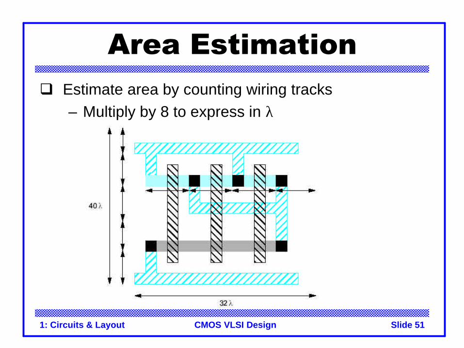
Area Estimationq Estimate area by counting wiring tracks
– Multiply by 8 to express in λ
1: Circuits & Layout Slide 52CMOS VLSI Design
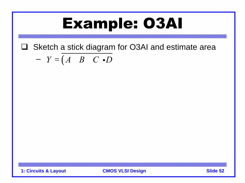
Example: O3AIq Sketch a stick diagram for O3AI and estimate area
– ( )Y A B C D= + + i
1: Circuits & Layout Slide 53CMOS VLSI Design
Example: O3AIq Sketch a stick diagram for O3AI and estimate area
– ( )Y A B C D= + + i
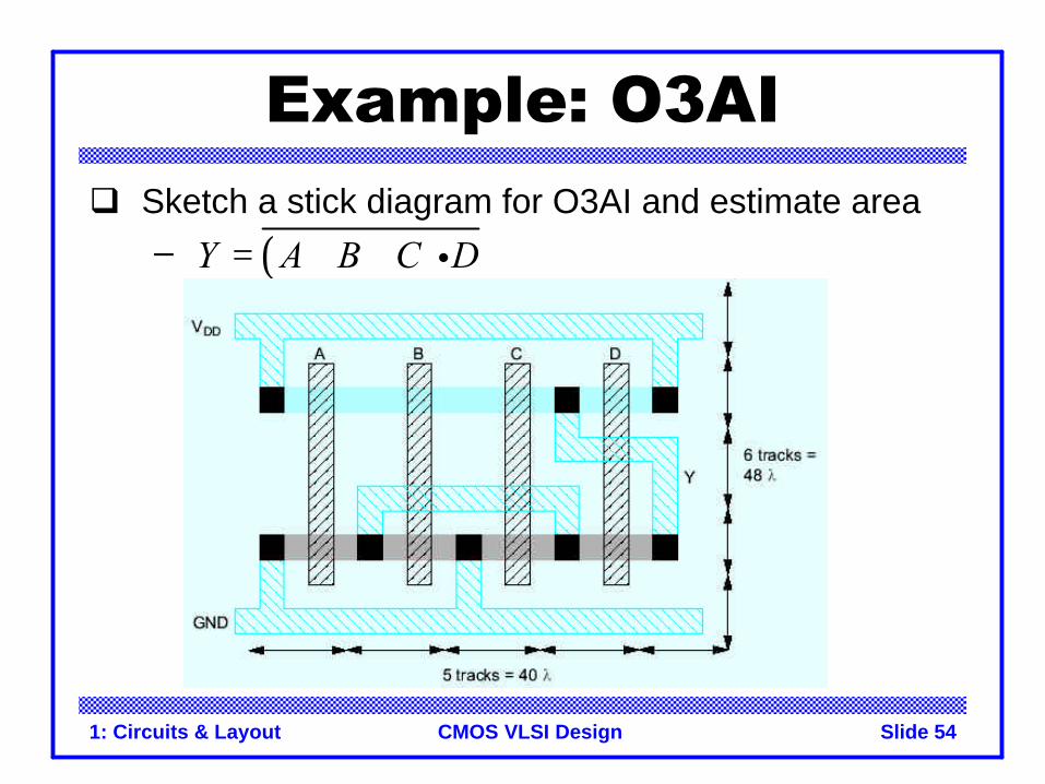
1: Circuits & Layout Slide 54CMOS VLSI Design
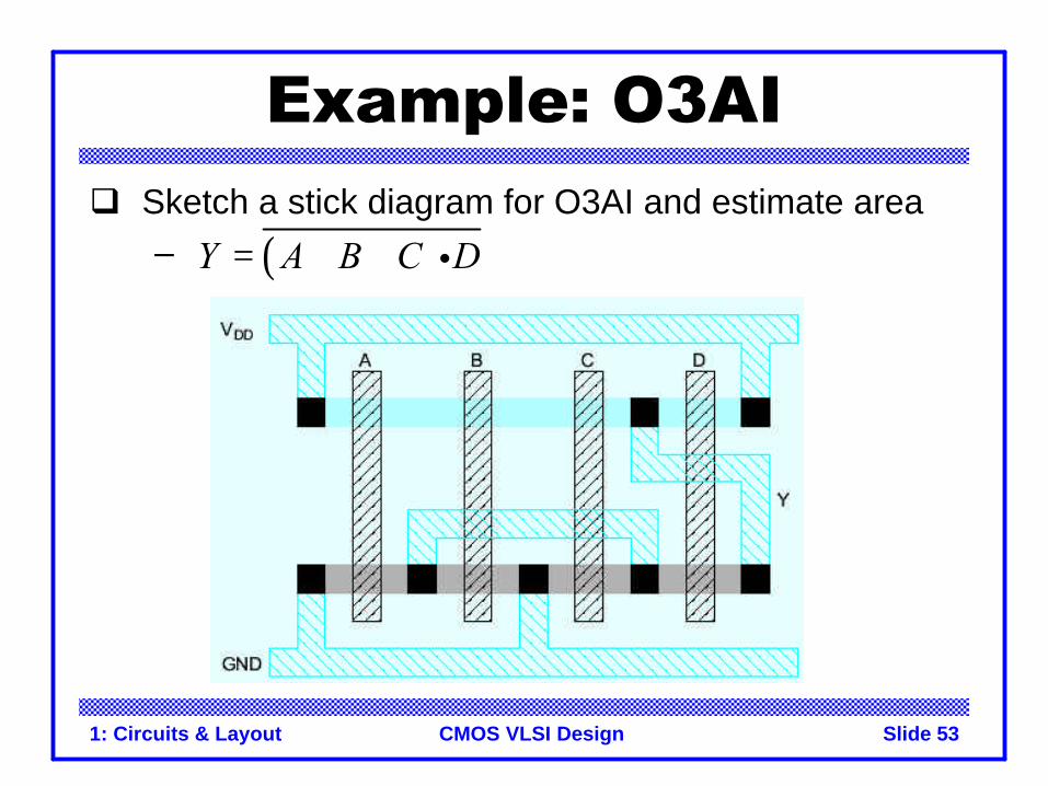
Example: O3AIq Sketch a stick diagram for O3AI and estimate area
– ( )Y A B C D= + + i


![THE SEMICONDUCTOR INTEGRATED CIRCUITS LAYOUT-DESIGN … · THE SEMICONDUCTOR INTEGRATED CIRCUITS LAYOUT-DESIGN ACT, 2000 ACT NO. 37 OF 2000 [4th September, 2000.] An Act to provide](https://img.pdfslide.us/doc/110x75/5fc601757488b351535ccb44/the-semiconductor-integrated-circuits-layout-design-the-semiconductor-integrated.jpg)