Embed Size (px)
Citation preview

Gold in Solar CellsA REVIEW OF CURRENT WORK
Edward W. WilliamsCentral Research Laboratories, Thorn EMI Limited, Hayes, U.K.
The cost of producing electricity from solar energy by means of solarcells is still high and limits the use of such devices to special situations.Gold has important roles not only in older types of cells but also in newertypes which are being developed to achieve increased efficiencies.
Solar cells are solid state generators that providecurrent by direct conversion of sunlight into electricalenergy. These devices literally rose,to fame when thefirst satellites were launched and space research ex-periments were powered by them. As we enter the1980's, solar cells are still playing a key role in power-ing satellites and the few trials with alternatives areunlikely to be repeated after the experience in 1978 ofthe problems associated with the uncontrolled re-entry above Canada of a nuclear-powered satellite.
During the space race of the 1960's, the use of goldfor contacts and connections in solar cells was thenorm because price was no object and because goldhas such high electrical conductivity and resistance tocorrosion. The latten property means that gold con-tacts and connectors are reliable in use; it also makesit easy to bond gold to itself and other metals in elec-tronic devices (1). Now that solar cells have comedown to Barth and the race is on to develop cheaperand cheaper products, gold contacts are betoming lesscompetitive for use in silicon single crystal p-n junc-tion devices.
The target of the United States Department ofEnergy is to produce solar cell modules at a cost ofU.S. $0.70 per watt by 1986 (2). If this goal is to beachieved with the current technology using singlecrystal cells, in which near-perfect arrangement of theatoms in the crystals and high purity are necessary,the price of the contact material and the package mustbe kept as low as possible, because the crystal-growing processes that have been developed arerelatively expensive. However, using the new,cheaper materials and processes that are emerging,gold, gold-plated or gold-clad contacts could becomemore common again (3).
There are solar cells, other than those based onsilicon single crystals, in which gold has an importantplace. In the Schottky barrier, gold plays a key role asa part of the heart of the device. In concentrator cellswhich operate at high temperature, gold contacts canbe used with single crystal p-n junction cells such as
those made from gallium arsenide (GaAs). Also,experimental cells with new materials often use goldcontacts because their properties are so reproducible.
The p-n Junction Solar CellsBefore discussing the mode of operation of p-n junc-
tion and other solar cells, it is appropriate to definesome of the terms that will be used in this connection.
The Fermi level of a solid is the energy level belowwhich all electron states are full of electrons, and inn -type material to which electron-donating impurities— for instance, phosphorus, arsenic or antimony insilicon — are added in controlled quantities, theFermi level is close to, or within, the conductionband. In the conduction band, electrons are free tomove, but in the valence or bonding band they arebound together with the atoms of the crystal and onlythe holes can move. Holes are positive charges whichoccur where electrons are missing. They are producedwhen impurities which deplete the valence band ofelectrons — for instance boron, aluminium, galliumor indium in silicon — are added to the crystal. E1,s isthe energy at the top of the valence band and E cs isthe energy at the bottom of the conduction band. Theenergy gap Eg of a semiconductor crystal is the energydifferente between E Va and Eca . Electron- or hole-current flow does not occur in this gap and so it issometimes referred to as the forbidden gap.
The value of Eg determines to a large extent theproperties of the semiconductor and for sunlight ab-sorption the optimum is 1.5 eV, which corresponds toa wavelength of light of 827 nm. Silicon, which todate has been the most commonly used material in p-njunction cells because it was developed so far in ad-vance of any other semiconductor material, has anenergy gap of 1.1 eV and is not the ideal material forhighly efficient solar devices.
A p-n junction cell is illustrated in Figure 1 beforeand after incidente of sunlight. In (a) the cell is in thedark. There can be no net current flow because theFermi level shown by the dotted line has the same
90

energy on both sides of the junction. 1B is the heightof the potential barrier at the junction between the p-and p-type materials. In Figure 1(b), light of energyequal to or greater than Eg shines on the crystal andgenerates electron-hole pairs at the junction: electronsare excited out of the valence band into the conduc-tion band and leave holes behind. These electrons cannow travel down the barrier, as shown by the arrow,and drop into empty states in the conduction band.Some of these photogenerated electrons are shown asnegative charges in the conduction band. Similarly,the photogenerated holes move up the barrier and areshown by the additional positive charges. In this non-equilibrium situation, with the light shining on thecrystal, the Fermi level on the n side is separated fromthe Fermi level on the p side by qV, where q is theelectron charge and V is the generated photovoltage.Since the quasi Fermi level on the n-side is close tothe conduction band, the potential barrier at the junc-tion between the n- and p-type materials is now reduc-ed to (D B — qV. The photocurrent flows from the p side(positive charge- or hole-dominated) to the n side(negative charge- or electron-dominated). Thus, a cur-rent is generated which flows in the opposite direc-tion to that flowing through the junction when light isexcluded by packaging or encapsulation and thedevice is used as an ordinary semiconductor diodewith the positive terminal of the power supply con-nected to the p side.
In order to collect the photocurrent, two electrodeswhich make ohmic contact to both the front and backof the cell are required. Ohmic contacts are junctionswhich are not sensitive to light and which in this casemust also be low in resistance. The back electrode isthe less critical and is usually made relatively thick inorder to keep the resistance low. The front electrodewhich contacts the n-type semiconductor region, hasto collect photogenerated carriers efficiently andtransmit sunlight to such an extent that cell efficiencyis not reduced appreciably. To achieve this, the frontelectrode must either consist of a conductive filmwhich is thin enough over the central area of the cellto be transparent to light, and thick enough at theedges to facilitate current collection, or it must consistof a thick conductive mesh bonded to the cell surface.In the Jatter case, the mesh may be created by a photo-engraving process. The calculation of the optimummesh size is not simple. Electrical resistance, lighttransmission and cell area must be optimized. Nor-mally, compromise values for the thicknesses of theelectrode and the mesh gaps are established fromtheory. Irrespective of the design of front electrodeused, gold is the conductive material of choice. It isreproducible from a resistivity and fabrication pointof view, and solar cells having a very high yield can beproduced using it. Moreover, an added advantage of
10
0R
ECe ________ FERMI LEVEL____
Eva
(b)
=PHOïOCURRENT
Fig. 1 Generation of a photovoltage V at a p-n junc-tion in a semiconductor.(a) At equilibriuin in the Bark, the Fermi level isconstant through the junction.(h) In sunlight, electron-hole pairs are generated hyphotons at, or near, the junction and the Fermilevels in this non-equilibrium condition are displac-ed by qV, where q is the electron charge and V is thegenerated photo -voltage
gold is that it is corrosion-resistant and can stand thehigh temperatures to which some cells are subjected.
In addition, the front surface of the cell is finishedwith an anti-reflection coating. This is a very thin,optically transparent film that 'traps' the sunlight byreducing reflection losses and thereby increases theefficiency of the cell. The thickness of this film has tobe accurately controlled and must be very uniform. Ifit is pinhole-free, it also protects from environmentalpollution that portion of the front surface of the cellwhich is exposed by the mesh spaces.
91

U
Fig. 2 Comparison of the load characteristics of aCu2S/CdS p-n junction solar cell in sunlight witli the`dark' current-voltage curve of the cell under for•werd bias,, that is when 'thë p side of the, junction 9sconneeted to the positive of a bauery. Voc is theopen circuit photovoltage and Isc is the short circuitphotocurrent
Fig. 3 Caleulatlon of the efficiency of a Cu 2S/CdSp-c junction soiar teil [rom iis load characteristics
Figure 2 compares the normai current-voltage (I-V)relationship of a p-n junction (its dark characteristics)with that when it operates in the solar mode (its lightcharacteristics). The light characteristics show the I-Vrelationship below the open circuit voltage, V oc,which is the voltage developed across the cell whenthere is no load resistor across it. The characteristicsfor voltages between 0 and V oc are measured after theintroduction of a variable load resistor across the cell.For this reason, curves such as the bottom one of
30
z20
110
ENERGY GAP. eV
Fig, 4 Varlation of tbc iheoreticab efficiency with theenergy gap E® of the material used for p-n junctionsolar cells
Figure 2 are sometimes referred to as the loadcharacteristics to avoid confusing them with the fullI-V characteristics, which are obtained by applyingboth positive and negative bias by means of a batteryor power supply placed across the junction. Discus-sion here is restricted to the load characteristics.
The short circuit current, I sc, is the current withthe cell shorted out with zero load resistance. I sc isdirectly proportional to the light intensity, whereasVOC saturates when this reaches a `one sun' value, thatis 100 mW/em2. For all p-n junction solar cells, Iscdepends on both the area of the cell and the light in-tensity, and saturates at very high light intensities. Incontrast, Voc increases very rapidly at low intensitiesand then begins to level out at an intensity of aboutone third of the `one sun' value.
The calculation of the efficiency of a solar cellfrom its load characteristics is shown in Figure 3. Themaximum power point P, at which the cell worksmost efliciently, is determined by drawing thetangent APB to the curve such that AP = PB. (Thiscan be proved simply by theory (4)). The maximumpower in watts is then PC multiplied by PD. InFigure 3, this is equal to 0.323 W. As the cell area is7.4 x 7.4 cm, the power per unit area is 5.9 mW/cm 2 .
Since 100 mW/cm 2 is falling on the cell, its efficiencyis 5.9 per cent.
Silicon p-n junction solar cells with efficiencies wellin excess of 10 per cent are now made, but Bilicon willnever be the best material for high efficiency cellsbecause of its low energy gap. Figure 4 shows atheoretical curve of p-n junction solar cell efficiencyagainst energy gap value (5, 6). Silicon is compared toGaAs and CdTe, and it can be seen that these lattercompounds, which have an energy gap close to the
92

theoretical optimum, should make higher efficiencycells. This has been borne out by some initial ex-periments which have shown that GaAs p-n junctioncells with efficiencies of over 20 per cent can easily bemade (7). In the case of silicon, efficiencies up to only18 per cent have been achieved (8), after more thantwenty years of intensive research.
In concluding this schematic description of the p-njunction cell, it is worth mentioning two of its short-comings. First, as is obvious from what has been said,its output power is proportional to the sunlight inten-sity, so that in countries in which this varies, con-siderably less solar power will be obtained and it willbe difficult to run solar systems without batterybackup during the day. Secondly, the operatingtemperature of cells of this type is important becauseit affects their efficiency (Figure 5).
Cu2S/CdS Cells with Gold ContactsFor over twenty years, gold has been used in con-
tacts to polycrystalline copper sulphide/cadmiumsulphide (Cu 2S/CdS) p-n junction cells. It is used forthe front contact in the manner illustrated in Figure 6,which shows light falling on a low-cost flexible cell (9).
To prepare this type of device, a CdS film isdeposited onto a conductive substrate of metallizedpolyester by electrophoresis from a sol obtained bybubbling hydrogen sulphide into a solution of cad-mium acetate in water. Water is used in preferente toalcohol as medium because it has a high dielectricconstant and aqueous sols are therefore more stablethan sols in an alcohol. A CdS partiele size of about10 nm is aimed for, to inhibit flocculation whichwould preclude the formation of pinhole-free thinfilms. The water sol is diluted with an alcohol justbefore electrophoresis to prevent excessive oxygenand hydrogen emission at the electrodes. Anodic de-position onto a polyester electrode metallized withstainless steel is the most common procedure, butgold and platinum metallizations have also beentested. However, in the case of platinum, very pooradhesion caused film cracking during drying whenthe CdS film was baked in air to harden it afterdeposition. CdS films about 1.5 µm thick are usualbecause flexible, pinhole-free deposits of thisthickness can be prepared. The flexibility is requiredto allow use of cheap plastic substrates.
The Cu2S film is then evaporated onto the CdS andmust not be thicker than 200 nm or the light will notpenetrate to the junction region where the photocur-rent is generated. In order to complete the circuit,front and back contacts must be established with theCu2 S and CdS films respectively. The back contact isprovided by the metal film between the CdS and thepolyester support. The front contact must be shapedso that it screens off a minimum of the Cu 2 S film
TÉMPERATURE, °G
Fig. 5 Variation of the efficiency of a Cu2S/CdS p-njunction solar cell with tentperature
SOLAR LIGHT
Fig. 6 $thematic seetion of a Cu2S/4dSp-n junctionsolar eelt with a gold-plated copper meeli top eon-tact. The CdS layer Is deposited el'ectropboreticaljy
from incident sunlight and its `window geometry'must therefore be carefully designed. In practice,either a gold-plated copper mesh is bonded to theCu 2S with a gold-containing conductive epoxyadhesive or a pressure contact plate is applied ontothe front surface. The gold coating on the copper isdeposited either by electroplating or by ion plating(10). Screen printing of gold mesh contacts has alsobeen carried out successfully.
The colour photograph in Figure 7 shows ex-perimental coatings on 25 pm thick polyester films.Various designs of solar cells of this type have beenstudied, using both gold and other metals as the backcontact materials. Efficiencies have always been low,however, and much more work will be required if thedream of a low-cost flexible solar cell that can betnass-produced by a continuous process and storedeasily is to materialize. Moreover, gold electrodes on
93

Fig. 7 Thin films deposited on polyester for research on flexible solar cells. From right to left the films are CdS on steel,gold, copper and aluminium. In every case, except for the CdS film which was deposited eleetrophoretically hy the umethoddescribed in the text to a thickness of 1.5 µm, the films are 200 non thick
CdS were never found to be ohmic but were found toform effective Schottky barriers.
The Gold Schottky Barrier Solar CellThe solar cells discussed so far make use of the
photovoltaic effect across the interface between ap-and an n-type semiconductor. Schottky barrier solarcells rely upon a similar effect across the interfacebetween a metal and a semiconductor.
Fig. 8 Scheinatic cross-section of a gold Schotikybarrier solar cell
The cross-section of one type of gold Schottky bar-rier solar cell is shown in Figure 8. The device con-sists of a 5 to 20 nm thick gold film which iseyaporated or ion-plated onto the freshly etched sur-face of an n-type semiconductor. A thicker gold con-tact dot is then evaporated onto the gold electrode andthe sequence is completed by an anti-reflection oxidecoating to increase the absorption of light, andthereby enhance the efficiency of the cell. A goldwire, attached to the contact dot by thermocompres-sion bonding, collects the current from the front orgold side of the cell and the circuit is closed by a con-nection to the back or semiconductor side of the cell.
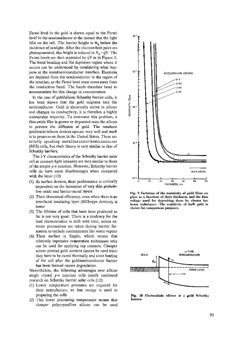
The thickness and structure of the gold film are im-portant, since its resistivity must be as low as possibleand it must be transparent to solar light. Thesignificance in this latter regard of the deposition pro-cess and conditions is clearly shown by the set ofcurves in Figure 9, in which the resistivity of goldfilms on glass is plotted as a function of thickness andof the bias voltages used in ionized-cluster beamevaporation technology (11). Clearly, films formedwith a 4 kV bias consisted of close packed gold atomsand gave the lowest resistance.
The energy band diagram shown in Figure 10 in-dicates how a current flow is generated in a goldSchottky barrier exposed to light. For simplicity, the
94
10-3
E
> 10 -aH
Wir
10 -5
Fermi level in the gold is shown equal to the Fermilevel in the semiconductor at the instant that the lightfalls on the cell. The barrier height is (I) $ before theincidence of sunlight. After the electron-hole pairs arephotogenerated, this height is reduced to 4) B — qV. TheFermi levels are then separated by qV as in Figure 1.The band bending and the depletion region where itoccurs can be understood by considering what hap-pens at the metal/semiconductor interface. Electronsare depleted from the semiconductor in the region ofthe junction, so the Fermi level must move away fromthe conduction band. The bands therefore bend toaccommodate for this change in concentration.
In the case of gold/silicon Schottky barrier cells, ithas been shown that the gold migrates into thesemiconductor. Gold is electrically active in siliconand changes its conductivity, it is therefore a highlyundesirable impurity. To overcome this problem, athin oxide film is grown or deposited onto the siliconto prevent the diffusion of gold. The resultantgold/oxide/silicon devices operate very well and workis in progress on them in the United States. These arestrictly speaking metal/insulator/semiconductor(MIS) cells, but their theory is very similar to that ofSchottky barriers.
The I-V characteristics of the Schottky barrier solarcell at constant light intensity are very similar to thoseof the simple p-n junction. However, Schottky barriercells do have some disadvantages when comparedwith the latter (12):(I) As surface devices, their performance is critically
dependent on the formation of very thin pinhole-free oxide and barrier-metal layers
(2) Their theoretical efficiency, even when there is aninterfacial insulating layer (MIS-type devices), islower
(3) The lifetime of cells that have been produced sofar is not very good. There is a tendency for theload characteristics to drift with time, unless ex-treme precautions are taken during barrier for-mation to exclude contaminants like water vapour
(4) Their surface is fragile, which means thatrelatively expensive evaporation techniques onlycan be used for applying top contacts. Cheaperscreen printed gold contacts cannot be used sincethey have to be cured thermally and since heatingof the cell after the gold/semiconductor barrierhas been formed causes degradation.
Nevertheless, the following advantages over siliconsingle crystal p-n junction cells justify continuedresearch on Schottky barrier solar cells (12):(1) Lower temperature processes are required for
their manufacture, so less energy is used inpreparing the cells
(2) This lower processing temperature means thatcheaper polycrystalline silicon can be used
10-2
BULK METAL
10 -6 L0
10 20 30 40 50 60THICKNESS, om
Fig. 9 Variation of the resistivity of gold films onglass as a function of their thiekness and the biasvoltage used for depositing theet by cluster ionbeam techniques. The resistivity of bulk gold isshown for comparison purposes
TYPEGOLDGOLD SEMICONDtJCTOR
— -- ----EERMI LEVEL —
r hm
Fig. 10 Photovoltaie effect s at a gold Schottkybarrier
95

because little diffusion of impurities along thegrain boundaries occurs
(3) Thin film preparation techniques such as ionplating (10) can be used to deposit in a singleoperation both the silicon and the gold layers on alow-cost substrate material. This process has thepotential of being very economical since it can bescaled up with a moving belt and moving elec-trode system
(4) There are some materials which cannot be madeboth p- and n-type, so Schottky barrier cells arethe only solar devices that can be made from them.
Gold in Experimental Solar CellsAfter reviewing in general terms the p-n junction
and the gold Schottky barrier cells, it is now time todiscuss some specific examples of how gold is beingused in a wide range of experimental solar modules.Since the use of gold is so extensive, the author haslimited this section to describing the work presentedat the Conference held in Luxembourg in September,1977 (13). A recent Solar Energy Research InstituteConference held in Denver (14) confirmed that mostof this research work with gold is continuing and evenexpanding.
Kipperman et al. (15) reported on a novelgold/silicon Schottky barrier cell formed on p-typesilicon. It was of the MIS-type and the novelty lay inthe way the silicon oxide was formed. Instead of usingthe conventional dry oxidation technique, theseauthors used a new hydrofluoric acid wet treatment toproduce a pinhole-free insulating layer between thesemiconductor and the gold. The oxidizing liquidwas prepared by dissolving SiO 2 in a 20 per centhydrofluoric acid solution for about two minutes.p-type silicon of conductivity 2 ohmcm was used andthe back contact was a titanium-gold alloy electrode.The thin transparent gold front electrode was DC-sputtered in argon at a pressure of 5.3 Pa. Finally, asmaller thick gold contact was added, so that strongelectrical contacts could be made to the front goldlayer. The thin gold electrode had a resistance in therange 14 to 20 ohms per square. Open circuit voltagesin excess of 300 mV were measured for the optimumoxide thickness and structure, but no efficiencyfigures were given. A trapping-assisted tunnellingmodel (16) was used to explain theoretically thebehaviour of these cells.
The Institute of Energy Conversion at the Univer-sity of Delaware has always used gold top contacts inwork on Cu 2S/CdS p-n junction solar cells. It is thelargest group working on solar devices and stillbelieves that evaporated CdS cells will be the firsttruly low-cost devices on the market. At Luxem-bourg, members of this group reported on an improv-ed gold top contact technology (17). To obtain a good
contact with the Cu 2S they evaporated a gold grid andthen pressure-bonded on top of this in an orthogonalarrangement another gold grid prepared by elec-trodeposition. The optical transmission of the hybridwas 91 per cent only, but the high current collectionefficiency thus achieved helped to raise the overallefficiency of the cells close to 8 per cent and goodreproducibility was obtained. The Delaware grouphas now reached close to 9 per cent efficiency usingfully evaporated gold grids with 95 per cent opticaltransmission and silicon monoxide anti-reflectioncoatings. Shorting-out problems with the current col-lection tab contact have been overcome by depositingan insulating layer under the tab.
The Delaware group used thick (20 to 40 µm)evaporated CdS coatings on zinc-plated coppersubstrates acting as back contacts, but a Germangroup (18) used for this purpose an evaporated silverfilm on a glass substrate. As top contact, a gold-platedcopper foil grid was bonded onto the Cu 2S and acover glass was then sealed down onto the grid insuch a way that total encapsulation was achieved. Noanti-reflection film was used and for large 7 x 7 cmcells, efficiencies of 4 per cent were achieved. It wasalso reported that the gold-plated grids were verystable under conditions where nickel-plated gridsshowed considerable degradation.
Gold is a very popular contact material for GaAssolar cells, because it appears to produce no con-tamination of the semiconductor. For example, in ap-n junction cell with a p-type GaA1As window, con-tacts have been made to the n-type GaAs base of thecell by means of evaporated gold-germanium alloy(19). With a titanium dioxide anti-reflection coating,an efficiency of 15.9 per cent was achieved under 'onesun' illumination.
GaA1As/GaAs cells for use in concentrated sunlightup to the 600 sun level and using gold in both thebottom and front electrodes were also described (20).Evaporated indium-germanium-gold alloys were usedfor contacts to the n-type base and titanium-goldalloys for contacts to the p-type front window. A gridpattern was photo-engraved onto the titanium-goldand the grid thickness was then increased to3 µm by gold electroplating. Anti-reflection coatingswere produced by anodizing the GaA1As window.The solar cell chips were mounted on standard tran-sistor headers and thermocompression-bonded goldwires were used to make contact to the header pins.Gold plating of the Kovar base gave low electrical andthermal resistance values.
Cadmium telluride (CdTe) which has an energygap close to the optimum for solar cells (see Figure 4),has received an increasing amount of attention recent-ly. Gold contacts to p-type CdTe in CdTe/CdS solarcells have been applied by two methods (21):
96

(1) Evaporation after etching of CdTe in sulphuricchromic acid solution. The gold film is then an-nealed in hydrogen at about 250°C
(2) Replacement from a gold chloride solution.The highest efficiency achieved with CdTe/CdS
cells was 7.9 per cent. In addition to CdTe/CdS cells,CdTe/Cu 2Te cells have been made and, in this lattercase, gold contacts were again deposited either byevaporation or from a gold chloride solution.
Gold Schottky barriers have been formed onevaporated polycrystalline films of cadmium selenide(CdSe) about 3 im thick (22). A 10 nm thick in-sulating layer which consisted of an oxide, a fluorideor a high energy gap semiconductor like zinc sulphidewas deposited on the CdSe before the transparentgold films were finally evaporated. The thickness ofthe gold contacts was not optimized, but it rangedfrom 10 to 30 nm giving an optical transmission of 50to 20 per cent. Gold was also used as the base contactin these experimental cells.
Two new semiconductor materials, tungstenselenide (WSe2) (23) and zinc phosphide (Zn 3P2) (24)have also been used for solar cells. WSe 2 has two ab-sorption edges, at 1.35 and 1.60 eV, and thus has anenergy gap very close to the theoretical optimum. Italso hns very good chemical stability. Gold Schottkybarriers have been formed on n-type single crystals ofWSe2 without an intentional oxide layer. A 5 nmthick gold film was used to give good opticaltransparency and an additional 100 nm of gold wasevaporated where a contact pad with the Schottkygold layer was required. The back contact was agallium-indium alloy and an efficiency of just over1 per cent was achieved without an anti-reflectioncoating. It is likely that WSe2 solar cells will bestudied more intensely in the future.
Work on p-type Zn 3 P 2, which is at a very earlystage, indicates that it has an energy gap of 1.4 eV,very close to the optimum for solar cells. Gold reactswith Zn 3P 2 and can only be used in MIS-type Schot-tky barrier configuration for top contacts. Iron ap-pears to be the best material for the base contacts andgood results have been obtained using it.
ConclusionsGold is playing a key role in solar cell research. It is
being used for contacts in a variety of devices and asan active consituent of Schottky barrier cells. Suchcells are the only kind that can be used in the case ofmany materials which do not display both p- andn -type conductivity.
In GaAs concentrator cells, gold is a reliable con-tact material which withstands the high operatingtemperatures resulting fror r concentration of sunlighton the cells. Under such circumstances, the high tostof gold is not an important consideration because the
area required is small in comparison with that of cellswhich do not use concentrated sunlight.
The use of gold in p-n junction cells of large area,like the Cu 2S/CdS thin film cells, will be restricted toa very thin gold coating, say 10 nm thick, depositedon the copper grid or on the Cu 2 S surface immediate-ly before the copper grid is applied. As far as siliconsolar cells are concerned, gold can be used in Schottkybarriers only when an insulating layer has been grownor deposited onto the silicon surface because ofchanges in electrical properties which are broughtabout by gold atoms which diffuse into the siliconcrystal lattice.
The adoption of new plating procedures in whichgold can be applied with very little waste will beessential if the metal is to be retained for commercialsolar cells as they become progressively cheaper in theyears to come. But in solar cells for space exploration,gold will probably have no competitor as the idealcontact and interconnection material because it is soreliable, so chemically inert and can tolerate the hightemperatures on satellite solar power `arms'.
References1 Anon., Gold Bull., 1972, 5, (2), 31.332 M. Prince, Solar Energy Research Institute Conference,
Denver, CO., 1979, Proceedings in press3 Texas Instrutnents advertisenient, Electron. Mag., 1979,
Sept. 27th4 F. A. Shirland, Adv. Energy Convers., 1966, 6,201-2225 J. Loferski, 1. Appl. Phys., 1956, 27, 777-7846 T. Mess, Rep. Prog. Phys., 1965, 28, 15.607 L. W. James and R. L. Moon, Appl. Phys. Lett., 1976,
28,150-1528 J. Lindmayer and J. F. Allison, 9th I.E.E.E. Photovoltaic
Spec. Conf., Silver Springs, U.S.A., 19729 E. W. Williams, K. Jones, A. J. Griffiths, D. J. Roughley,
J. M. Bel!, J. G. Steven, M. J. Huson, M. Rhodes andT. Costich, Sol. Cells, 1980, 1 (3), in press
10 E. W. Williams, Gold Bull., 1978, 11 (2), 30-3411 T. Takagi, I, Yamada and A. Sasaki, Solid State Electron.
Devices, Solar Cells Special Issue, 1978, 2, S40-S4812 Adapted from W. G. Townsend, Solid State Electron. Devices,
Solar Cells Special Issue, 1978, 1, S31-S3413 Commission of the European Communities, Photovoltaic
Solar Energy Conference, Luxembourg, September 1977, Pro-ceedings published by D. Reidel Publishing Co., 1978
14 Solar Energy Research Institute Conference, Denver, CO.,Sept. 1979, SERI/TP-311-428
15 A. H. M. Kipperman, S, C. M. Backerra, H. J. Maaskamp andR. J. C. van Zolingen, see (13), pp. 961-966
16 S. J. Fonash, J. Appl. Phys., 1979, 47, 3597; see also (15)17 A. M. Barnett, J. D. Meakin and A. Rothwarf, see (13),
pp. 535-54618 W, Arndt, G. Bilger, W. H. Bloss, G. H. Hewig, F. Pfisterer
and H. W. Schock, see (13), pp. 547-55619 E. Fabre, A. Briere and J. P. Andre, see (13), pp. 388-39420 J. W. Burgess, R. Davis, B. T. Debney and R. Nicklin,
see (13), pp. 395-40421 A. L. Fahrenburch, J. ,'-rcnovich, F. Courrages, S. Y. Yin and
R. H. Bube, see (13), pp. 608-61722 D. Bonnet, see (13), pp. 630-63723 C. Clemen, A. Moller, P. Muny, J. Honigschmid and
E. Bucher, see (13), pp. 638-64324 A. Catalano, V. Data, E. A. Dagen, R. B. Hall, J. V. Masi,
J. D. Meakin, G. Warfield and A. M. Barnett, see (13),pp. 644-653
97