Embed Size (px)
Citation preview
SILICONTEK CO., LTD.LCD Module Specification
PART NO. : STCE40200S1LYHB
Table of Contents
1. COVER & TABLE OF CONTENTS 1
2. RECORD OF REVISION 2
3. GENERAL SPECIFICATIONS 3
4. ABSOLUTELY MAXIMUM RATINGS 4
5. ELECTRICAL CHARACTERISTICS 5
6. ELECTRO-OPTICAL CHARACTERISTIC 5
7. TIMING CHARACTERISTICS 8
8. PIN CONNECTIONS 10
9. POWER SUPPLY 10
10. BLOCK DIAGRAM 11
11. QUALITY ASSURANCE 18
12. LOT NUMBERING SYSTEM 22
13. LCM NUMBERING SYSTEM 22
14. PRECAUTIONS FOR USING LCM 23
15. OUTLINE DRAWING 24
Approved by Checked by Checked by Drawn by
Pro.Div. R & D.Div.Final Revision: Sheet Code: Issued Date: Total Page:
24
Tel : 86-769-83623728 Fax : 86-769-83630806 Mail [email protected]
1/24
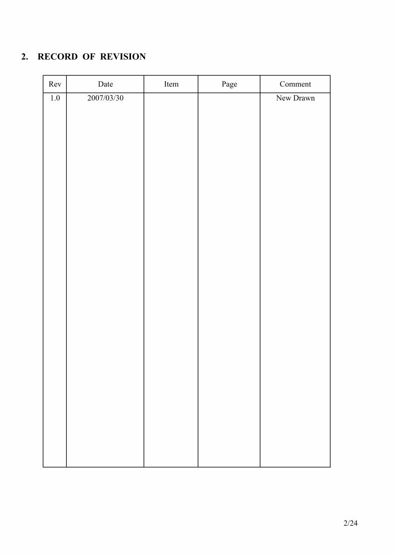
2. RECORD OF REVISION
Rev Date Item Page Comment
1.0 2007/03/30 New Drawn
2/24
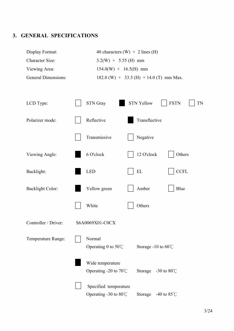
3. GENERAL SPECIFICATIONS
Display Format: 40 characters (W) × 2 lines (H)
Character Size: 3.2(W) × 5.55 (H) mm
Viewing Area: 154.0(W) × 16.5(H) mm
General Dimensions: 182.0 (W) × 33.5 (H) × 14.0 (T) mm Max.
LCD Type: STN Gray STN Yellow FSTN TN
Polarizer mode: Reflective Transflective
Transmissive Negative
Viewing Angle: 6 O'clock 12 O'clock Others
Backlight: LED EL CCFL
Backlight Color: Yellow green Amber Blue
White Others
Controller / Driver: S6A0069X01-C0CX
Temperature Range: Normal
Operating 0 to 50 Storage -10 to 60
Wide temperature
Operating -20 to 70 Storage -30 to 80
Specified temperature
Operating -30 to 80 Storage -40 to 85
3/24
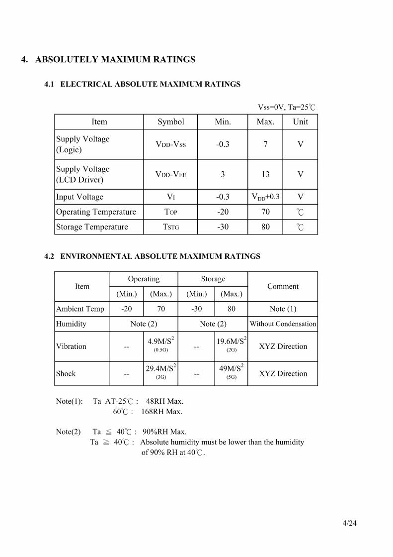
4. ABSOLUTELY MAXIMUM RATINGS
4.1 ELECTRICAL ABSOLUTE MAXIMUM RATINGS
Vss=0V, Ta=25
Item Symbol Min. Max. Unit
Supply Voltage(Logic) VDD-VSS -0.3 7 V
Supply Voltage(LCD Driver) VDD-VEE 3 13 V
Input Voltage VI -0.3 VDD+0.3 V
Operating Temperature TOP -20 70
Storage Temperature TSTG -30 80
4.2 ENVIRONMENTAL ABSOLUTE MAXIMUM RATINGS
ItemOperating Storage
Comment(Min.) (Max.) (Min.) (Max.)
Ambient Temp -20 70 -30 80 Note (1)
Humidity Note (2) Note (2) Without Condensation
Vibration -- 4.9M/S2
(0.5G) -- 19.6M/S2
(2G) XYZ Direction
Shock -- 29.4M/S2
(3G) -- 49M/S2
(5G) XYZ Direction
Note(1): Ta AT-25 : 48RH Max. 60 : 168RH Max.
Note(2) Ta ≦ 40 : 90%RH Max. Ta ≧ 40 : Absolute humidity must be lower than the humidity
of 90% RH at 40.
4/24

5. ELECTRICAL CHARACTERISTICS
Item Symbol Condition Min. TYP. Max. Unit
Supply Voltage(Logic)
VDD-VSS 4.75 5.0 5.25 V
Supply Voltage(LCD)
VDD-VEE
0 4.5 4.7 4.9
V25 4.3 4.5 4.7
50 4.1 4.3 4.5
Input VoltageVIH -- 0.7*VDD -- VDD
VVIL -0.3 -- 0.55
Logic SupplyCurrent
IDD VDD=3V -- 0.15 0.3 mA
6. ELECTRO-OPTICAL CHARACTERISTICS
Item Symbol Condition Min Typ. Max. Unit Ref.
Rise Time Tr0
--1100 1800
ns
Note(1)25 420 670
Fall Time Tf0
--210 340
ns25 100 300
Contrast CR 25 Note(3)
Viewing Angle θΦ
25&CR≧2
-30 -- 40Deg. Note(2)
-30 -- 30
Frame Frequency Ff 25 -- 64 -- HzNote (1)&(2): See next pageNote (3): Contrast ratio is defined under the following condition,
CR= Brightness of non-selected conditionBrightness of selected condition
(a). Temperature---------------25(b). Frame frequency----------64Hz(c). Viewing angle--------------θ=0°,φ=0°(d). Operating voltage---------4.5V
Intensity
Driving Voltage
B
Cr=B/A
Selected Dots
0%
Non-selected Dots
A
100%
5/24

Note (1) Response time is measured as the shortest period of time possible between the change in state of an LCD segment as demonstrated below:
Condition:( a ) . Temperature------------25( b ) . Frame frequency------64Hz( c ) . Viewing Angle------------θ=0°, φ=0°( d ) . Operating voltage-----4.5V
Note(2) Definition of Viewing Angle
Definition of Angle θ&ф Definition of Viewing Angle θ1&θ2
10%
90%
OFFONOFF
Tr Tf
Voltage Wave Form
T
Luminance
Cr
2
θθ1 θ2
6/24
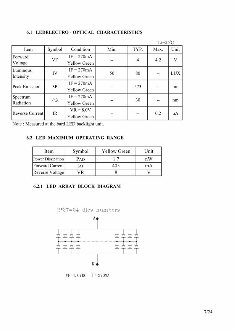
6.1 LEDELECTRO - OPTICAL CHARACTERISTICS
Ta=25Item Symbol Condition Min. TYP. Max. Unit
ForwardVoltage VF
IF = 270mA-- 4 4.2 V
Yellow GreenLuminousIntensity IV
IF = 270mA50 80 -- LUX
Yellow Green
Peak Emission λPIF = 270mA
-- 573 -- nmYellow Green
SpectrumRadiation λ
IF = 270mA-- 30 -- nm
Yellow Green
Reverse Current IRVR = 8.0V
-- -- 0.2 uAYellow Green
Note : Measured at the bard LED backlight unit.
6.2 LED MAXIMUM OPERATING RANGE
Item Symbol Yellow Green UnitPower Dissipation PAD 1.7 nWForward Current IAF 405 mAReverse Voltage VR 8 V
6.2.1 LED ARRAY BLOCK DIAGRAM
VF=4.0VDC IF=270MA
K
A
7/24
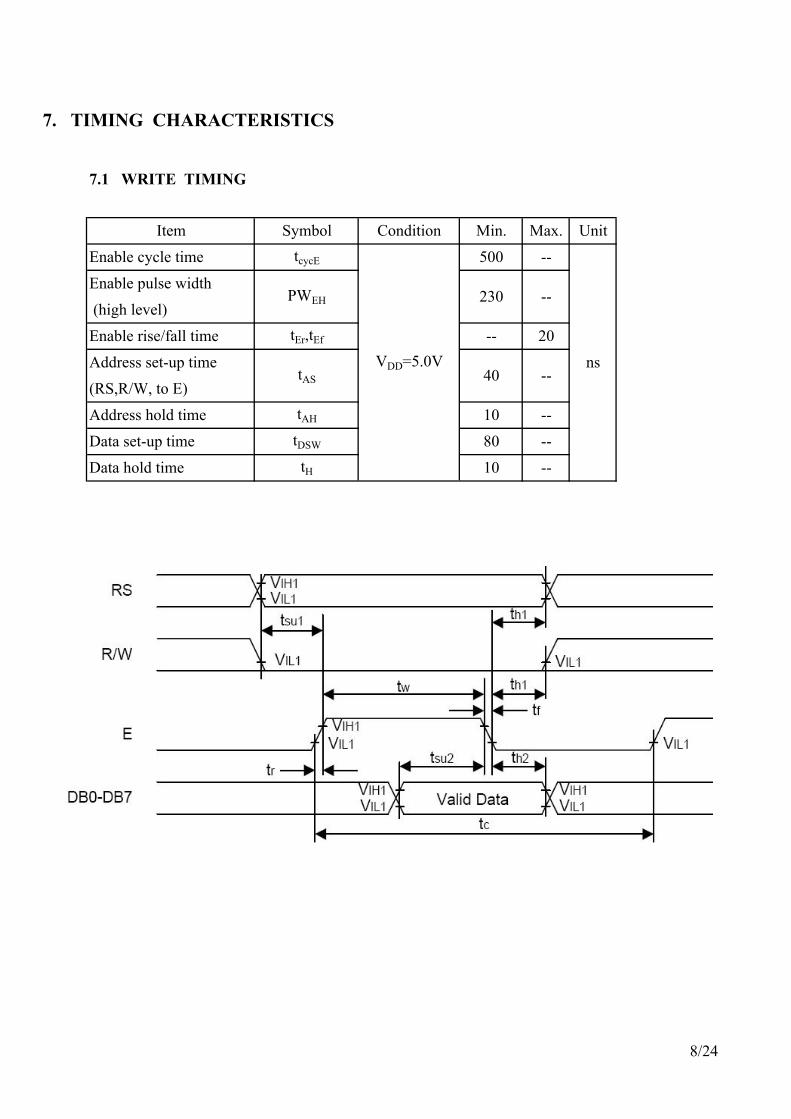
7. TIMING CHARACTERISTICS
7.1 WRITE TIMING
Item Symbol Condition Min. Max. Unit
Enable cycle time tcycE
VDD=5.0V
500 --
ns
Enable pulse widthPWEH 230 --
(high level)
Enable rise/fall time tEr,tEf -- 20
Address set-up timetAS 40 --
(RS,R/W, to E)
Address hold time tAH 10 --
Data set-up time tDSW 80 --
Data hold time tH 10 --
8/24
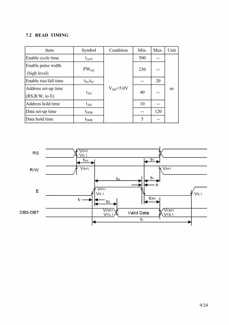
7.2 READ TIMING
Item Symbol Condition Min. Max. Unit
Enable cycle time tcycE
VDD=5.0V
500 --
ns
Enable pulse widthPWEH 230 --
(high level)
Enable rise/fall time tEr,tEf -- 20
Address set-up timetAS 40 --
(RS,R/W, to E)
Address hold time tAH 10 --
Data set-up time tDDR -- 120
Data hold time tDHR 5 --
9/24

8. PIN CONNECTIONS
No. Symbol Function1 VSS Ground, 0V 2 VDD Logic power supply, +5V3 VEE Voltage for LCD drive4 RS Data / Instruction register select5 R/W Read / Write6 E Enable signal, start data read/write7 DB0
Data Bus Line
8 DB19 DB210 DB311 DB412 DB513 DB614 DB715 A LED Anode, power supply "+"(DC +5V)16 K LED Cathode, power supply "-"
9. POWER SUPPLY
VDD
+5V
Vss
VR VEE
LED A+5V
LED K
VR=10KΩ
10/24
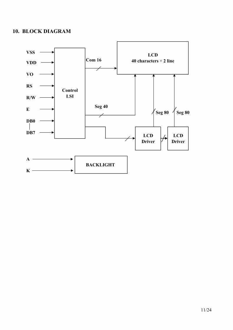
10. BLOCK DIAGRAM
LCD40 characters × 2 line
VSS
ControlLSI
VDD Com 16
VO
RS
R/W
E Seg 40 Seg 80 Seg 80
DB0
DB7 LCDDriver
LCDDriver
ABACKLIGHT
K
11/24

10.1 INSTRUCTIONS
InstructionCODE
DESCRIPTIONExecuted
Time(max)focs=250KHzRS R/W DB7 DB6 DB5 DB4 DB3 DB2 DB1 DB0
Clear Display 0 0 0 0 0 0 0 0 0 1 Clear all display and returns the cursor 1.53mSto the home position(Address 0)
Cursor At Home 0 0 0 0 0 0 0 0 1 *
Returns the cursor to the home position
1.53mS(Address 0). Also returns te display being shifted to the original position DDRAM contents remain unchanged.
Entry Mode Set 0 0 0 0 0 0 0 1 I/D SSets the cursor move direction and
39uSspecifies or not to shift the display. These operations are performed during data write and read.
Display On/OffControl 0 0 0 0 0 0 1 D C B
Sets the ON/OFF of all display (d) 39uScursor ON/OFF©, and blink of cursor
position character(B).Cursor/Display 0 0 0 0 0 1 S/C R/L * *
Moves the cursor and shifts the display39uS
Shift without changing DDRAM contents.
Function Set 0 0 0 0 1 DL N F * * Sets interface data length (DL), number 39uSof display lines(N) and character font(F)
CGRAM Address 0 0 0 1 ACGSets the CGRAM, data is sent and
39uSSet received after this setting.
DDRAM Address 0 0 1 ADDSets the CGRAM,data is sent and
39uSSet received after this setting.
Busy Flag/ AddressRead 0 1 BF AC
Reads Busy flag (FB) indicating
0uSindicating internal operation is being performed and reads address counter contents.
CGRAM/DDRAM 1 0 WRITE DATAWrites data into DDRAM
43uSData Write or CGRAM
CGRAM/DDRAM 1 1 READ DATAReads data into DDRAM
43uSData Read or CGRAM
Code Description Executed Time(max.)I/D=1: Increment DL=0:4-bit DDRAM: Display Data RAM Fcp or focs=250kHzI/D=0: Decrement 1/16 duty CGRAM: Characfter Generator RAM However, when frequency S=1: With display shift 1/18 duty, 1/11 duty ACG: CGRAM Address changes, execution timeS/C=1: Display shift F=1:5x10 dots ADD: DDRAM Address also changesS/C=0: Cursor movement F=0:5x7 dots corresponds to cursor address ExampleR/L=1: Shift to the right BF=1: Internal Operation is being performed AC: Address Counter, used for both If fcp or focs is 270kHzR/L=0: Shift to the left BF=0: Instruction acceptable DDRAM and CGRAM
40 uS * 250 = 37 uSD/L=1: 8-bit *: Invalid 270
12/24
0
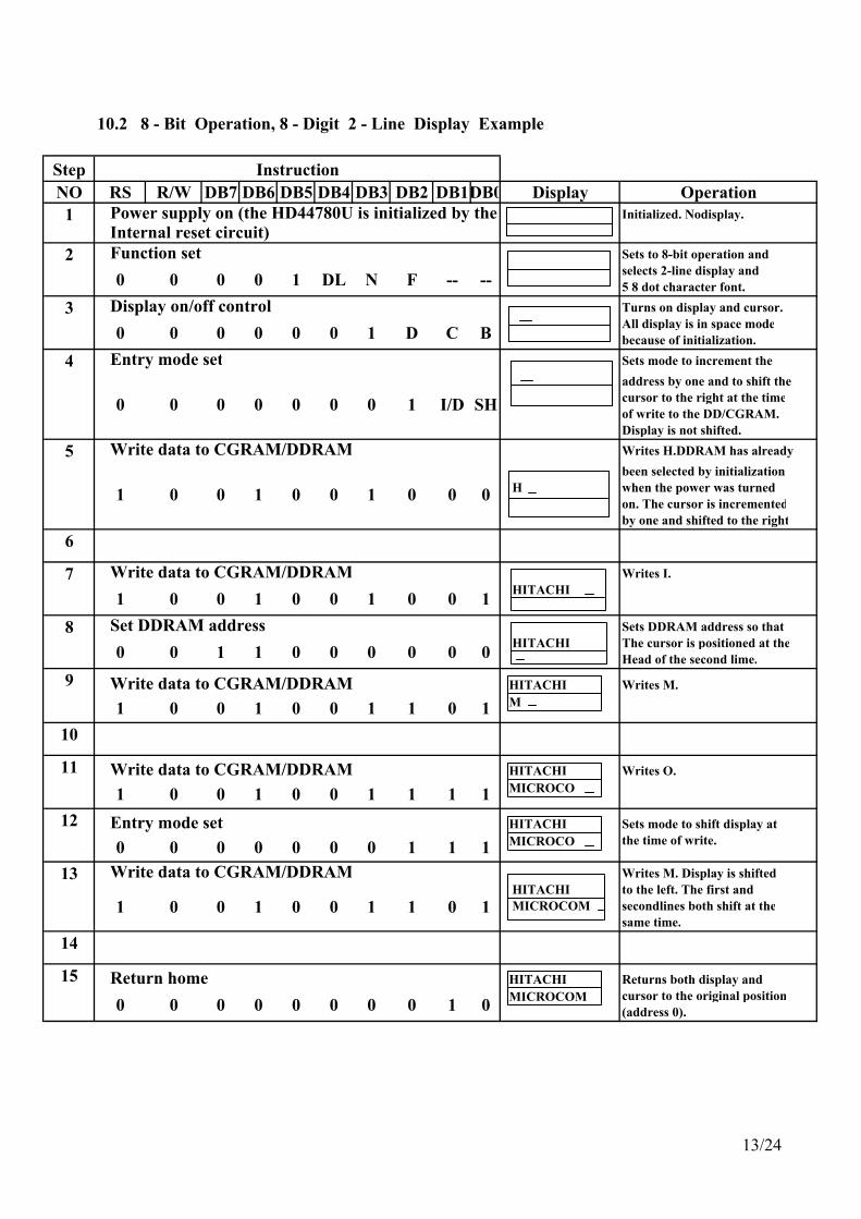
10.2 8 - Bit Operation, 8 - Digit 2 - Line Display Example
Step InstructionNO RS R/W DB7 DB6 DB5 DB4 DB3 DB2 DB1DB Display Operation1 Power supply on (the HD44780U is initialized by the Initialized. Nodisplay.
Internal reset circuit)2 Function set Sets to 8-bit operation and
0 0 0 0 1 DL N F -- -- selects 2-line display and5 8 dot character font.
3 Display on/off control Turns on display and cursor.
0 0 0 0 0 0 1 D C B All display is in space modebecause of initialization.
4 Entry mode set Sets mode to increment the
0 0 0 0 0 0 0 1 I/D SHaddress by one and to shift thecursor to the right at the timeof write to the DD/CGRAM.Display is not shifted.
5 Write data to CGRAM/DDRAM Writes H.DDRAM has already
1 0 0 1 0 0 1 0 0 0been selected by initialization
H when the power was turnedon. The cursor is incrementedby one and shifted to the right
6
7 Write data to CGRAM/DDRAM Writes I.
1 0 0 1 0 0 1 0 0 1 HITACHI
8 Set DDRAM address Sets DDRAM address so that
0 0 1 1 0 0 0 0 0 0 HITACHI The cursor is positioned at theHead of the second lime.
9 Write data to CGRAM/DDRAM HITACHI Writes M.
1 0 0 1 0 0 1 1 0 1 M
10
11 Write data to CGRAM/DDRAM HITACHI Writes O.
1 0 0 1 0 0 1 1 1 1 MICROCO
12 Entry mode set HITACHI Sets mode to shift display at
0 0 0 0 0 0 0 1 1 1 MICROCO the time of write.
13 Write data to CGRAM/DDRAM Writes M. Display is shifted
1 0 0 1 0 0 1 1 0 1 HITACHI to the left. The first and MICROCOM secondlines both shift at the
same time.
14
15 Return home HITACHI Returns both display and
0 0 0 0 0 0 0 0 1 0 MICROCOM cursor to the original position(address 0).
13/24
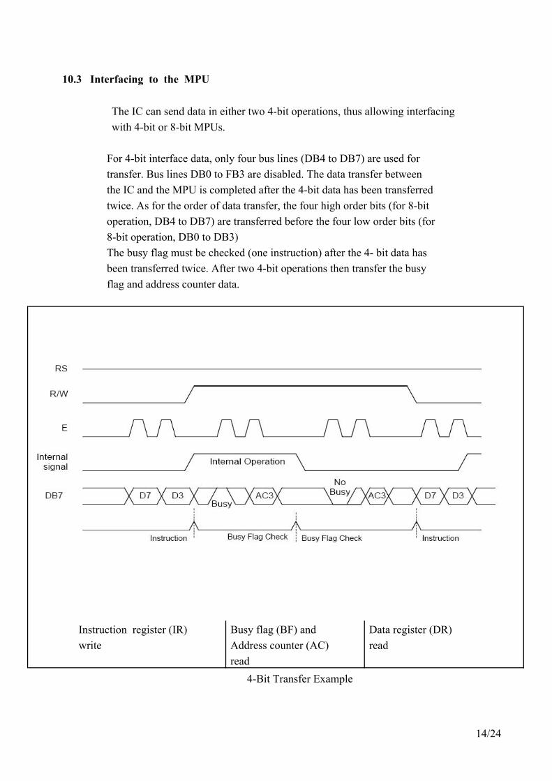
10.3 Interfacing to the MPU The IC can send data in either two 4-bit operations, thus allowing interfacing with 4-bit or 8-bit MPUs.
For 4-bit interface data, only four bus lines (DB4 to DB7) are used for transfer. Bus lines DB0 to FB3 are disabled. The data transfer betweenthe IC and the MPU is completed after the 4-bit data has been transferredtwice. As for the order of data transfer, the four high order bits (for 8-bit operation, DB4 to DB7) are transferred before the four low order bits (for8-bit operation, DB0 to DB3)The busy flag must be checked (one instruction) after the 4- bit data hasbeen transferred twice. After two 4-bit operations then transfer the busyflag and address counter data.
Instruction register (IR) Busy flag (BF) and Data register (DR)write Address counter (AC) read
read4-Bit Transfer Example
14/24

10.4 1-LINE Display
Displayposition 1 2 3 4 5 6 7 8 9 10 11 12 13 14 15 16
00 01 02 03 04 05 06 07 40 41 42 43 44 45 46 47DDRAMAddress(hexadecimal)
16 1- Line
2-LINE Display
Displayposition 1 2 3 4 5 . 8 . . . . . 16 . . . 20 . . . 24 . . . 39 40
00 01 02 03 04 26 27DDRAMAddress 40 41 42 43 44 66(hexadecimal) 67
8 2-Line
16 2-Line
20 2-Line
24 2-Line
15/24
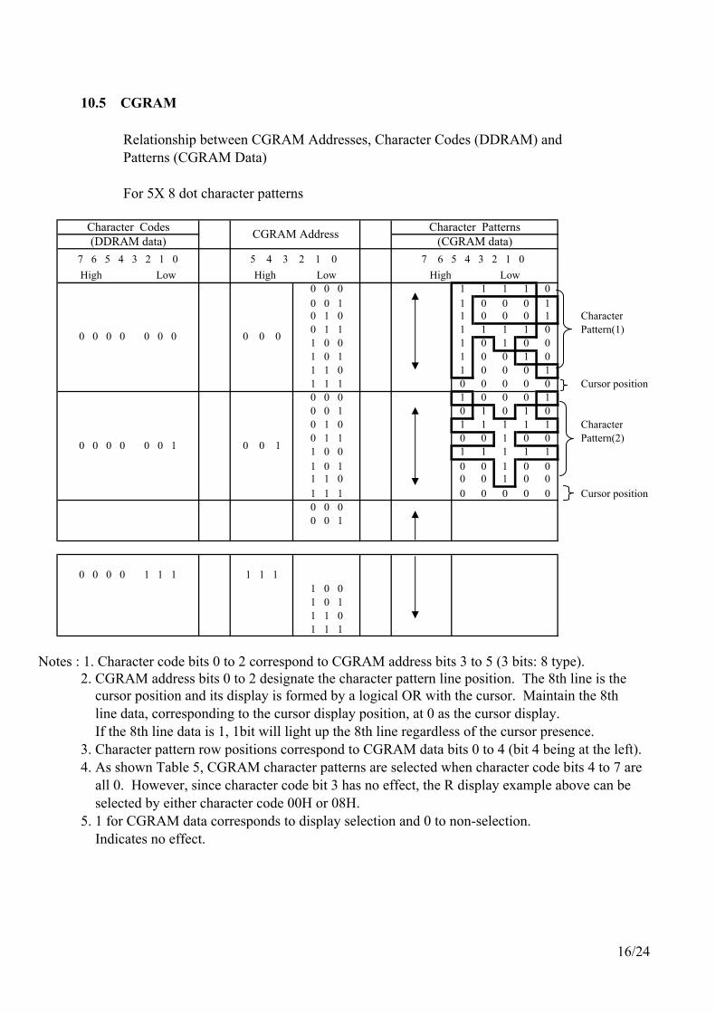
10.5 CGRAM
Relationship between CGRAM Addresses, Character Codes (DDRAM) andPatterns (CGRAM Data)
For 5X 8 dot character patterns
Character Codes CGRAM Address Character Patterns(DDRAM data) (CGRAM data)
7 6 5 4 3 2 1 0 5 4 3 2 1 0 7 6 5 4 3 2 1 0 High Low High Low High Low
0 0 0 0 0 0 0 0 0 0
0 0 0 1 1 1 1 00 0 1 1 0 0 0 10 1 0 1 0 0 0 1 Character0 1 1 1 1 1 1 0 Pattern(1)1 0 0 1 0 1 0 01 0 1 1 0 0 1 01 1 0 1 0 0 0 11 1 1 0 0 0 0 0 Cursor position
0 0 0 0 0 0 1 0 0 1
0 0 0 1 0 0 0 10 0 1 0 1 0 1 00 1 0 1 1 1 1 1 Character0 1 1 0 0 1 0 0 Pattern(2)1 0 0 1 1 1 1 11 0 1 0 0 1 0 01 1 0 0 0 1 0 01 1 1 0 0 0 0 0 Cursor position0 0 00 0 1
0 0 0 0 1 1 1 1 1 11 0 01 0 11 1 01 1 1
Notes : 1. Character code bits 0 to 2 correspond to CGRAM address bits 3 to 5 (3 bits: 8 type). 2. CGRAM address bits 0 to 2 designate the character pattern line position. The 8th line is the
cursor position and its display is formed by a logical OR with the cursor. Maintain the 8th line data, corresponding to the cursor display position, at 0 as the cursor display. If the 8th line data is 1, 1bit will light up the 8th line regardless of the cursor presence.3. Character pattern row positions correspond to CGRAM data bits 0 to 4 (bit 4 being at the left).4. As shown Table 5, CGRAM character patterns are selected when character code bits 4 to 7 are all 0. However, since character code bit 3 has no effect, the R display example above can be selected by either character code 00H or 08H.5. 1 for CGRAM data corresponds to display selection and 0 to non-selection. Indicates no effect.
16/24
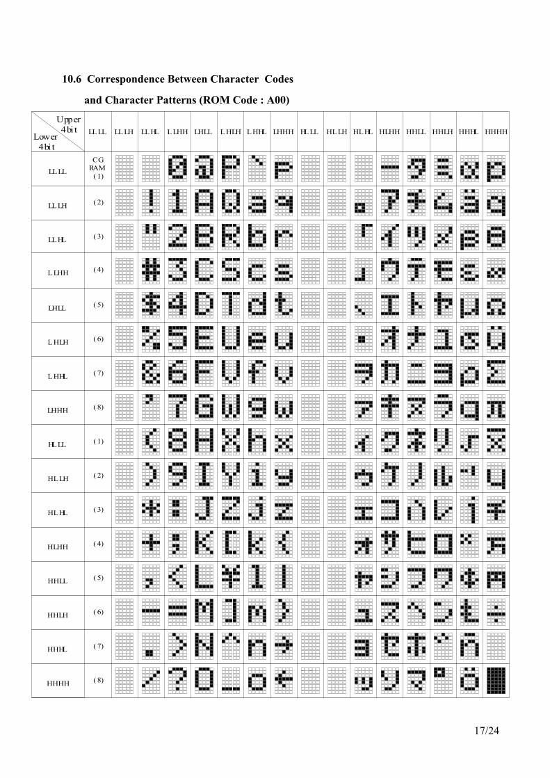
10.6 Correspondence Between Character Codes
and Character Patterns (ROM Code : A00)
HLHH
HLLH
HHHH
HHHL
HHLH
HHLL
HLHH
HLHL
( 8)
( 7)
( 6)
( 4)
( 5)
( 3)
HL LL
LHHH
L HHL
L HLH
LHLL
L LHH
( 2)
( 1)
( 8)
( 7)
( 6)
( 5)
( 4)
LL HL
LL LH
LLLL
Lower4bi t
LLHLLL LHLL LL
( 3)
( 2)
CGRAM
( 1)
Upper4bi t LHHHLHHLL HLHLHLLLLHH HLHLHLLHHLLL HHHHHHHLHHLHHHLL
17/24
11. QUALITY ASSURANCE
11.1 Test Condition
11.1.1 Temperature and Humidity(Ambient Temperature)Temperature : 25±2Humidity : 65±5%
11.1.2 Operation Unless specified otherwise, test will be conducted under function state.
11.1.3 ContainerUnless specified otherwise, vibration test will be conducted to the product itself without putting it in a container.
11.1.4 Test FrequencyFor destructive tests, such as shock test, will be conducted only once.
11.1.5 Test Method
No. Parameter conditions Regulations1 High Operating Temperature 70±2 Note 32 Low Operating Temperature -20±2 Note 33 High Storage Temperature 80±2 Note 34 Low Storage Temperature -30±2 Note 3
5
Vibration Test Total fixed amplitude : 1.5mm Note 3(Non-operation state) Vibration Frequency : 10 - 55Hz
One cycle 60 seconds to 3 directionsof X.Y.Z. for each 15 minutes
6 Damp Proof Test 40±2, 90 - 95%RH, 96h Note 1,2(Non-operation state)
7 Shock Test To be measured after drop from 60cm height Note 3(Non-operation state) to concrete surface in packaged stateNote 1: Returned to normal temperature and humidity for 4 hrs.Note 2: No dew condensation to be observed.Note 3: No change on display and in operation under the test condition
18/24

11.2 Inspection Condition
11.2.1 Inspection conditions
The LCD shall be inspected under 40W white fluorescent light.The distance between the eyes and the sample shall be morethan 30cm. All directions for inspecting the sample should bewithin 45° against perpendicular line.
11.2.2 Definition of applicable Zones
11.2.2.1. COB
11.2.2.2. Heat Seal
11.2.2.3. TAB and COG
45
Metal (Platic) Frame
LCD Glass
Bottom Polarizer
Backlight
Upper Polarizer
Conductive Rubber
PCB
Foot (Frame) Coating Epoxy
PCB
Metal (Plastic) Frame
LCD
Gasket
LCD
Heat Seal
ITO Terminal Pad
IC
TAB COG
LCD Glass LCD Glass
IC
Pin
19/24
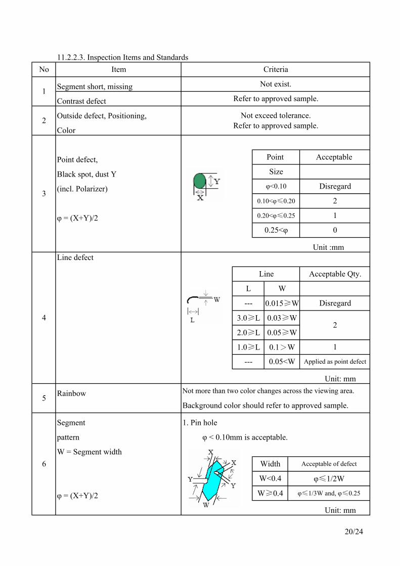
11.2.2.3. Inspection Items and StandardsNo Item Criteria
1 Segment short, missing Not exist.
Contrast defect Refer to approved sample.
2 Outside defect, Positioning, Not exceed tolerance.Refer to approved sample.Color
3
Point defect, Point Acceptable
Black spot, dust Y Size
(incl. Polarizer) φ<0.10 Disregard
0.10<φ≤0.20 2
φ = (X+Y)/2 0.20<φ≤0.25 1
0.25<φ 0
Unit :mm
4
Line defect
Line Acceptable Qty.
L W
--- 0.015≥W Disregard
3.0≥L 0.03≥W2
2.0≥L 0.05≥W
1.0≥L 0.1>W 1
--- 0.05<W Applied as point defect
Unit: mm
5 Rainbow Not more than two color changes across the viewing area.
Background color should refer to approved sample.
6
Segment 1. Pin hole
pattern φ < 0.10mm is acceptable.
W = Segment width Width Acceptable of defect
W<0.4 φ≤1/2W
φ = (X+Y)/2 W≥0.4 φ≤1/3W and, φ≤0.25
Unit: mm
20/24
No Item Criteria
φ = (X+Y)/2
2. Segment width acceptable.
A - B < 0.20 ; D≤0.2
C≤0.1 E≤0.15
3. Dot pattern
Size Acceptable Qty.
φ<0.10 Disregard
0.10≤φ≤0.20 1
φ>0.20 0
C: Shall not touch adjacent dot.
Unit: mm
7 Polarizer air bubble
Size Acceptable Qty.
φ<0.30 or B Zone Disregard
0.30≤φ≤0.50 2
0.50<φ≤0.80 1
φ>0.80 0
Unit: mm
8 Polarizer miss-placement
1. Not in excess of outside dimension of the LCD
unit (refer to mechanical drawing).
2. No miss-placement exposing the viewing
area. (V.A.)
21/24
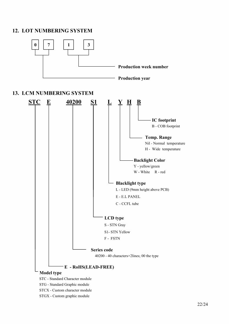
12. LOT NUMBERING SYSTEM
0 7 1 3
Production week number
Production year
13. LCM NUMBERING SYSTEM
STC E 40200 S1 L Y H B
IC footprintB - COB footprint
Temp. RangeNil - Normal temperature H - Wide temperature
Backlight ColorY - yellow/greenW - White R - red
Blacklight typeL - LED (9mm height above PCB)
E - E.L PANEL
C - CCFL tube
LCD typeS - STN Gray
S1- STN Yellow
F - FSTN
Series code 40200 - 40 characters×2lines; 00 the type
E - RoHS(LEAD-FREE)Model typeSTC - Standard Character moduleSTG - Standard Graphic moduleSTCX - Custom character moduleSTGX - Custom graphic module
22/24
14. PRECAUTION FOR USING LCM
1. LIQUID CRYSTAL DISPLAY (LCD)LCD is made up of glass, organic sealant, organic fluid, and (5). The normal static prevention measures should be Polymer based polarizers. The following precautions should observed for work clothes and working benches; for theBe taken when handing, latterconductive(rubber) mat is recommended.(1). Keep the temperature within range of use and storage. (6). Since dry air is inductive to static, a relative Excessive temperature and humidity could cause Polarization humidity of 50-60% is recommended.degredation, polarizer peel off or bubble.(2). Do not contact the exposed polarizers with anything harder 2.3 Soldering than an HB pencil lead. To clean dust off the display surface, (1). Solder only to the I/O terminals.wipe gently with cotton, chamois or other soft material soaked (2). Use only soldering irons with proper grounding andin petroleum benzin. no leakage.(3). Wipe off saliva or water drops immediately. Contact with (3). Soldering temperature: 280±10over a long period of time may cause polarizer deformation or (4). Soldering time: 3 to 4 sec.color fading, while an active LCD with water condensation on (5). Use eutectic solder with resin flux fill. its surface will cause corrosion of ITO electrodes. (6). If flux is used, the LCD surface should be cove to(4). Glass can be easily chipped or cracked from rough handling, avoid flux spatters. Flux residue should be removed after especially at corners and edges. wards.(5). Do not drive LCD with DC voltage.
2.4 Operation2. Liquid Crystal Display Modules (1). The viewing angle can be adjusted by varying the LCD2.1 Mechanical Considerations driving voltage V0.LCM are assembled and adjusted with a high degree of precision. (2). Driving voltage should be kept within specified range; Avoid excessive shocks and do not make any alterations or excess voltage shortens display life.modifications. The following should be noted. (3). Response time increases with decrease in temperature.(1). Do not tamper in any way with the tabs on the metal frame. (4). Display may turn black or dark blue at temperatures(2). Do not modify the PCB by drilling extra holes, changing its above its operational range; this is (however not pressing on outline, moving its components or modifying its pattern. the viewing area) may cause the segments to appear (3). Do not touch the elastomer connector, especially insert an “fractured”. backlight panel (for example, EL). (5). Mechanical disturbance during operation (such(4). When mounting a LCM make sure that the PCB is not under pressing on the viewing area) may cause the segment any stress such as bending or twisting. Elastomer contacts are appear “fractured”.very delicate and missing pixels could result from slight dislocation of any of the elements. 2.5 Storage (5). Avoid pressing on the metal bezel, otherwise the elastomer If any fluid leaks out of a damaged glass cell, wash off any connector could be deformed and lose contact, resulting in human part that comes into contact with soap and water.missing pixels. Never swallow the fluid. The toxicity is extremely low but
caution should be exercised at all time.2.2 Static ElectricityLCM contains CMOS LSI’s and the same precaution for such 2.6 Limited Warranty devices should apply, namely Unless otherwise agreed between S-TEK and customer,(1). The operator should be grounded whenever he/she comes S-TEK will replace or repair any of its LCD and LCM into contact with the module. Never touch any of the conductive whichis found to be defective electrically and visually when partssuch as the LSI pads, the copper leads on the PCB and the inspected in accordance with S-TEK acceptance standards,interface terminals with any parts of the human body. for a period of one year from date of shipment. Confirmation (2). The modules should be kept in antistatic bags or other of such dateshall be based on freight documents. The containers resistant to static for storage. warranty liability of S-TEK is limited to repair and/or(3). Only properly grounded soldering irons should be used. replacement onthe terms set forth above. S-TEK will not (4). If an electric screwdriver is used, it should be well grounded responsible for any subsequent or consequential events.and shielded from commutator sparks.
23/24
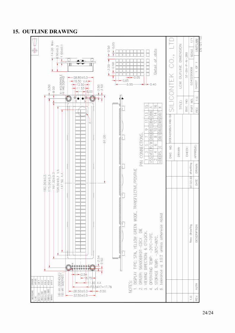
15. OUTLINE DRAWING
24/24