Embed Size (px)
Citation preview
LC Series Transmitter Module
Data Guide
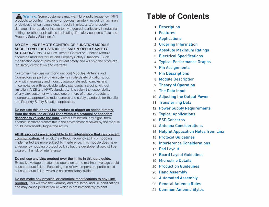
! Table of Contents 1 Description 1 Features 1 Applications 2 Ordering Information 2 Absolute Maximum Ratings 3 Electrical Specifications 4 Typical Performance Graphs 7 Pin Assignments 7 Pin Descriptions 8 Module Description 9 Theory of Operation 9 The Data Input 10 Adjusting the Output Power 11 Transferring Data 12 Power Supply Requirements 12 Typical Applications 13 ESD Concerns 14 Antenna Considerations 15 Helpful Application Notes from Linx 15 Protocol Guidelines 16 Interference Considerations 17 Pad Layout 17 Board Layout Guidelines 19 Microstrip Details 20 Production Guidelines 20 Hand Assembly 20 Automated Assembly 22 General Antenna Rules 24 Common Antenna Styles
Warning: Some customers may want Linx radio frequency (“RF”) products to control machinery or devices remotely, including machinery or devices that can cause death, bodily injuries, and/or property damage if improperly or inadvertently triggered, particularly in industrial settings or other applications implicating life-safety concerns (“Life and Property Safety Situations”).
NO OEM LINX REMOTE CONTROL OR FUNCTION MODULE SHOULD EVER BE USED IN LIFE AND PROPERTY SAFETY SITUATIONS. No OEM Linx Remote Control or Function Module should be modified for Life and Property Safety Situations. Such modification cannot provide sufficient safety and will void the product’s regulatory certification and warranty.
Customers may use our (non-Function) Modules, Antenna and Connectors as part of other systems in Life Safety Situations, but only with necessary and industry appropriate redundancies and in compliance with applicable safety standards, including without limitation, ANSI and NFPA standards. It is solely the responsibility of any Linx customer who uses one or more of these products to incorporate appropriate redundancies and safety standards for the Life and Property Safety Situation application.
Do not use this or any Linx product to trigger an action directly from the data line or RSSI lines without a protocol or encoder/decoder to validate the data. Without validation, any signal from another unrelated transmitter in the environment received by the module could inadvertently trigger the action.
All RF products are susceptible to RF interference that can prevent communication. RF products without frequency agility or hopping implemented are more subject to interference. This module does have a frequency hopping protocol built in, but the developer should still be aware of the risk of interference.
Do not use any Linx product over the limits in this data guide. Excessive voltage or extended operation at the maximum voltage could cause product failure. Exceeding the reflow temperature profile could cause product failure which is not immediately evident.
Do not make any physical or electrical modifications to any Linx product. This will void the warranty and regulatory and UL certifications and may cause product failure which is not immediately evident.
!
– –1
LC Series Transmitter Module
Data Guide
Revised 3/18/14
DescriptionThe LC Series is ideally suited for volume use in OEM applications such as remote control, security, identification and periodic data transfer. Housed in a compact surface-mount package, the LC Series transmitter utilizes a highly-optimized SAW architecture to achieve an unmatched blend of performance, size, efficiency and cost. When paired with a matching LR Series receiver, a highly reliable wireless link is formed, capable of transferring serial data at distances of up to 3,000 feet. No external RF components are required (except an antenna), making design and integration straightforward, even for engineers without previous RF experience.
Features• Low cost• No external RF components
required• Ultra-low power consumption• Compact surface-mount package• Stable SAW-based architecture• Supports data ranges to
5,000bps• Wide supply range (2.7 to
5.2VDC)• Direct serial interface• Low harmonics• No production tuning
Applications• Remote control• Keyless entry• Garage/gate openers• Lighting control• Medical monitoring/call systems• Remote industrial monitoring
• Periodic data transfer• Home/industrial automation• Fire/security alarms• Remote status/position sensing• Long-range RFID• Wire elimination
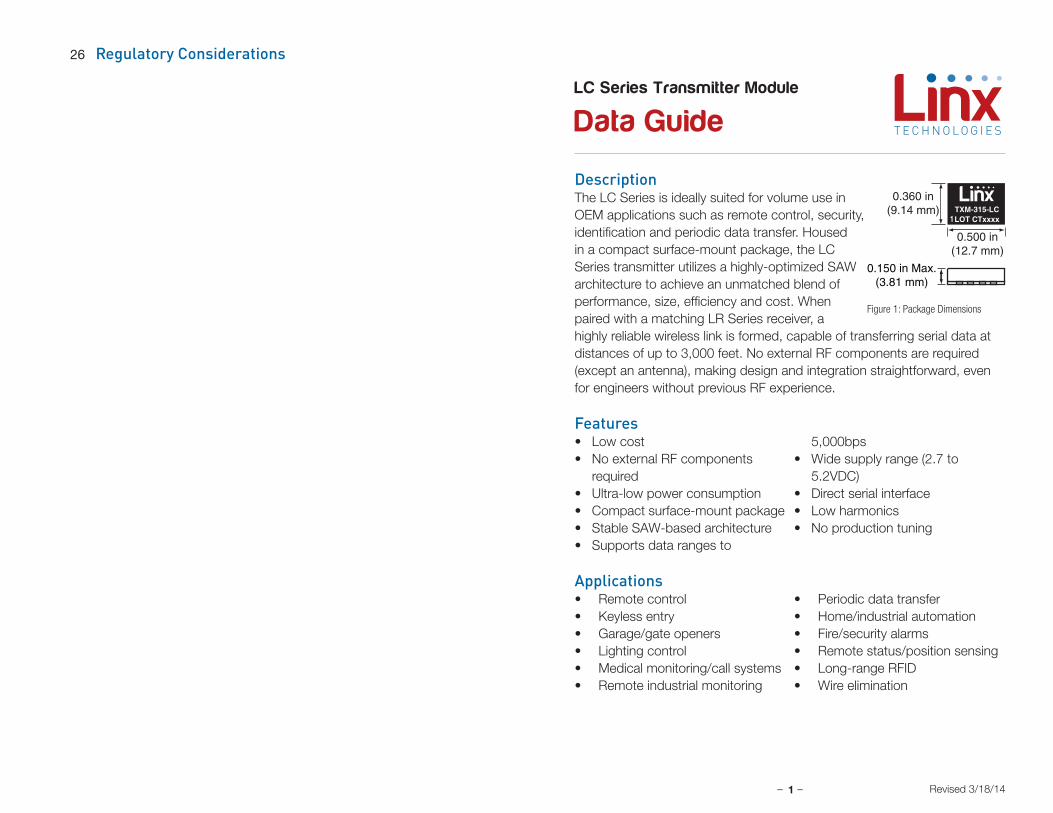
TXM-315-LCLOT CTxxxx
0.360 in(9.14 mm)
0.500 in(12.7 mm)
0.150 in Max.(3.81 mm)
26 Regulatory Considerations
Figure 1: Package Dimensions
– – – –2 3
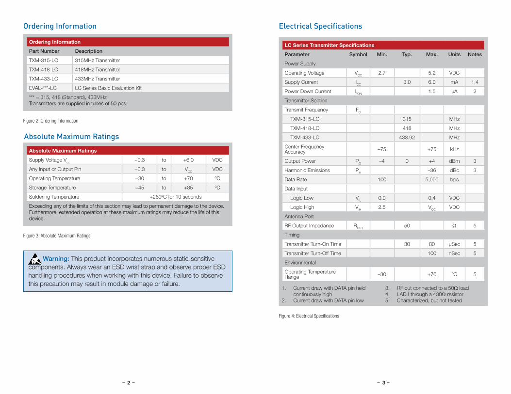
LC Series Transmitter Specifications
Parameter Symbol Min. Typ. Max. Units Notes
Power Supply
Operating Voltage VCC 2.7 5.2 VDC
Supply Current lCC 3.0 6.0 mA 1,4
Power Down Current lPDN 1.5 µA 2
Transmitter Section
Transmit Frequency FC
TXM-315-LC 315 MHz
TXM-418-LC 418 MHz
TXM-433-LC 433.92 MHz
Center Frequency Accuracy –75 +75 kHz
Output Power PO –4 0 +4 dBm 3
Harmonic Emissions PH –36 dBc 3
Data Rate 100 5,000 bps
Data Input
Logic Low VIL 0.0 0.4 VDC
Logic High VIH 2.5 VCC VDC
Antenna Port
RF Output Impedance ROUT 50 Ω 5
Timing
Transmitter Turn-On Time 30 80 µSec 5
Transmitter Turn-Off Time 100 nSec 5
Environmental
Operating Temperature Range –30 +70 ºC 5
Electrical Specifications
1. Current draw with DATA pin held continuously high
2. Current draw with DATA pin low
3. RF out connected to a 50Ω load4. LADJ through a 430Ω resistor5. Characterized, but not tested
Ordering Information
Ordering Information
Part Number Description
TXM-315-LC 315MHz Transmitter
TXM-418-LC 418MHz Transmitter
TXM-433-LC 433MHz Transmitter
EVAL-***-LC LC Series Basic Evaluation Kit
*** = 315, 418 (Standard), 433MHzTransmitters are supplied in tubes of 50 pcs.
Figure 2: Ordering Information
Absolute Maximum Ratings
Absolute Maximum Ratings
Supply Voltage Vcc −0.3 to +6.0 VDC
Any Input or Output Pin −0.3 to VCC VDC
Operating Temperature −30 to +70 ºC
Storage Temperature −45 to +85 ºC
Soldering Temperature +260ºC for 10 seconds
Exceeding any of the limits of this section may lead to permanent damage to the device. Furthermore, extended operation at these maximum ratings may reduce the life of this device.
Figure 3: Absolute Maximum Ratings
Warning: This product incorporates numerous static-sensitive components. Always wear an ESD wrist strap and observe proper ESD handling procedures when working with this device. Failure to observe this precaution may result in module damage or failure.
Figure 4: Electrical Specifications
– – – –4 5
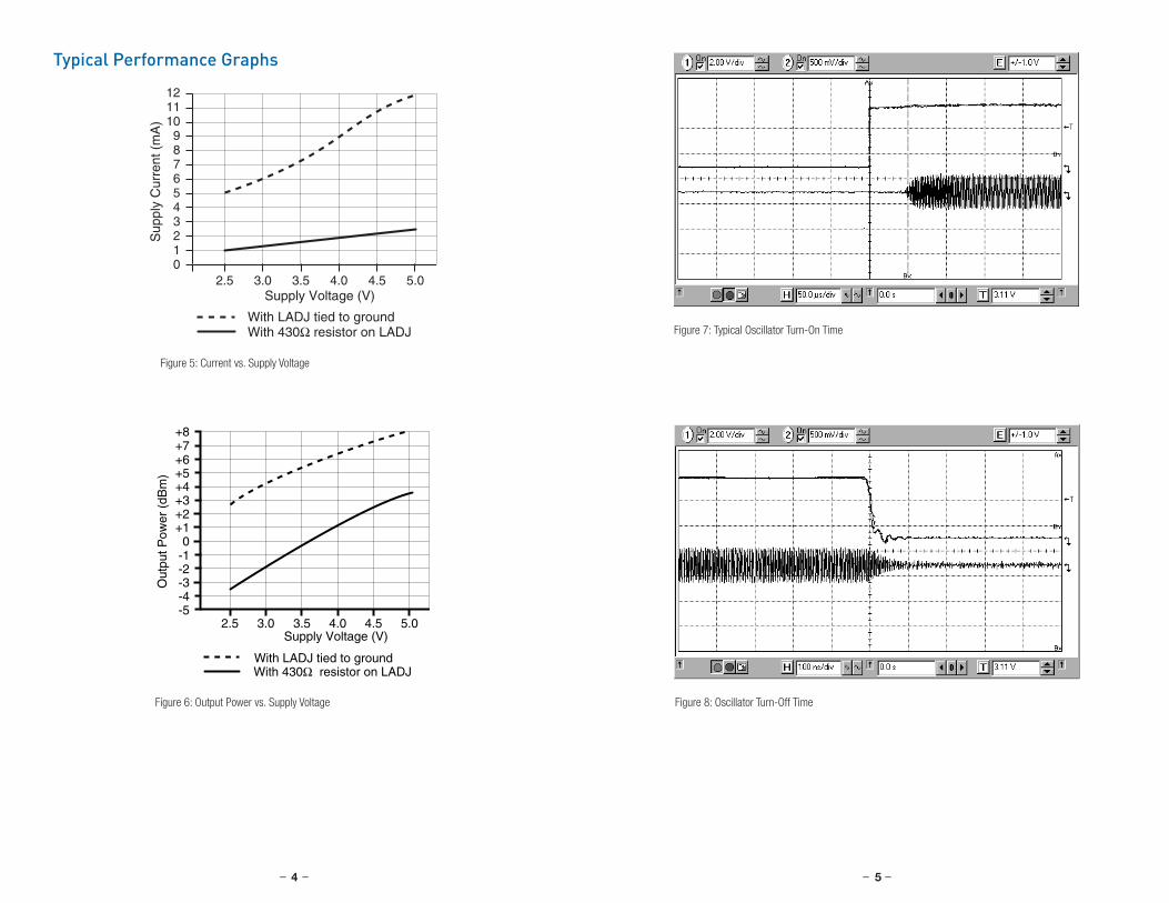
Typical Performance Graphs
2.5 3.0 3.5 4.0 4.5 5.0Supply Voltage (V)
1
32
456789
101112
0
With 430Ω resistor on LADJWith LADJ tied to ground
Sup
ply
Cur
rent
(m
A)
0-1
-4-5
2.5 3.0 3.5 4.0 4.5
-2-3
Supply Voltage (V)
+1
+3+2
+4+5+6+7+8
5.0
With 430Ω resistor on LADJWith LADJ tied to ground
Out
put P
ower
(dB
m)
Figure 5: Current vs. Supply Voltage
Figure 6: Output Power vs. Supply Voltage
Figure 7: Typical Oscillator Turn-On Time
Figure 8: Oscillator Turn-Off Time
– – – –6 7
+8+7+6+5+4+3+2+1
0-1-2-3-4
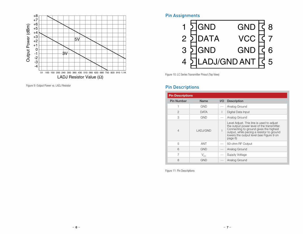
LADJ Resistor Value (Ω)51 100 150 200 240 300 360 430 510 560 620 680 750 820 910 1.1K
Out
put P
ower
(dB
m)
3V
5V
Pin Assignments
GNDDATAGND GND
ANTLADJ/GND
GNDVCC
1234 5
678
Pin Descriptions
Pin Number Name I/O Description
1 GND — Analog Ground
2 DATA I Digital Data Input
3 GND — Analog Ground
4 LADJ/GND I
Level Adjust. This line is used to adjust the output power level of the transmitter. Connecting to ground gives the highest output, while pacing a resistor to ground lowers the output level (see Figure 9 on page 6)
5 ANT — 50-ohm RF Output
6 GND — Analog Ground
7 VCC — Supply Voltage
8 GND — Analog Ground
Pin DescriptionsFigure 9: Output Power vs. LADJ Resistor
Figure 10: LC Series Transmitter Pinout (Top View)
Figure 11: Pin Descriptions
– – – –8 9
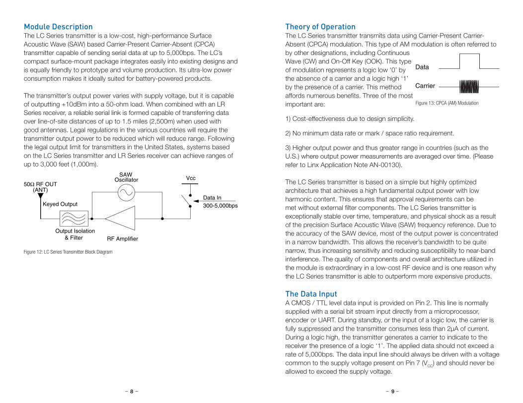
Module DescriptionThe LC Series transmitter is a low-cost, high-performance Surface Acoustic Wave (SAW) based Carrier-Present Carrier-Absent (CPCA) transmitter capable of sending serial data at up to 5,000bps. The LC’s compact surface-mount package integrates easily into existing designs and is equally friendly to prototype and volume production. Its ultra-low power consumption makes it ideally suited for battery-powered products.
The transmitter’s output power varies with supply voltage, but it is capable of outputting +10dBm into a 50-ohm load. When combined with an LR Series receiver, a reliable serial link is formed capable of transferring data over line-of-site distances of up to 1.5 miles (2,500m) when used with good antennas. Legal regulations in the various countries will require the transmitter output power to be reduced which will reduce range. Following the legal output limit for transmitters in the United States, systems based on the LC Series transmitter and LR Series receiver can achieve ranges of up to 3,000 feet (1,000m).
Output Isolation & Filter RF Amplifier
Keyed Output
Vcc SAW Oscillator
Data In300-5,000bps
50Ω RF OUT(ANT)
Theory of OperationThe LC Series transmitter transmits data using Carrier-Present Carrier-Absent (CPCA) modulation. This type of AM modulation is often referred to by other designations, including Continuous Wave (CW) and On-Off Key (OOK). This type of modulation represents a logic low ‘0’ by the absence of a carrier and a logic high ‘1’ by the presence of a carrier. This method affords numerous benefits. Three of the most important are:
1) Cost-effectiveness due to design simplicity.
2) No minimum data rate or mark / space ratio requirement.
3) Higher output power and thus greater range in countries (such as the U.S.) where output power measurements are averaged over time. (Please refer to Linx Application Note AN-00130).
The LC Series transmitter is based on a simple but highly optimized architecture that achieves a high fundamental output power with low harmonic content. This ensures that approval requirements can be met without external filter components. The LC Series transmitter is exceptionally stable over time, temperature, and physical shock as a result of the precision Surface Acoustic Wave (SAW) frequency reference. Due to the accuracy of the SAW device, most of the output power is concentrated in a narrow bandwidth. This allows the receiver’s bandwidth to be quite narrow, thus increasing sensitivity and reducing susceptibility to near-band interference. The quality of components and overall architecture utilized in the module is extraordinary in a low-cost RF device and is one reason why the LC Series transmitter is able to outperform more expensive products.
The Data InputA CMOS / TTL level data input is provided on Pin 2. This line is normally supplied with a serial bit stream input directly from a microprocessor, encoder or UART. During standby, or the input of a logic low, the carrier is fully suppressed and the transmitter consumes less than 2µA of current. During a logic high, the transmitter generates a carrier to indicate to the receiver the presence of a logic ‘1’. The applied data should not exceed a rate of 5,000bps. The data input line should always be driven with a voltage common to the supply voltage present on Pin 7 (VCC) and should never be allowed to exceed the supply voltage.
Figure 12: LC Series Transmitter Block Diagram
Data
Carrier
Figure 13: CPCA (AM) Modulation
– – – –10 11
Adjusting the Output PowerDepending on the type of antenna being used and the duty cycle of the data, the output power of the LC Series transmitter module may be higher than FCC regulations allow. The output power of the module is intentionally set high to compensate for losses resulting from inefficient antennas that may be used to realize cost or space savings. Since attenuation is often required, it is generally wise to provide for its implementation and allow the FCC test lab to easily attenuate the transmitter to the maximum legal limit for your product.
Two methods of attenuation are available using the LC Series transmitter module. First, a resistor may be placed between Pin 4 (LADJ) and ground to achieve up to a 7dB reduction in output power. The resistor value is easily determined from Figure 9 on page 6. Do not exceed the resistance values shown as transmitter instability may result. This method can also be used to reduce the transmission range and power consumption.
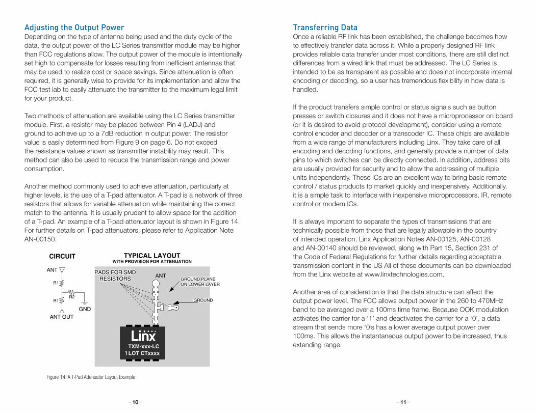
Another method commonly used to achieve attenuation, particularly at higher levels, is the use of a T-pad attenuator. A T-pad is a network of three resistors that allows for variable attenuation while maintaining the correct match to the antenna. It is usually prudent to allow space for the addition of a T-pad. An example of a T-pad attenuator layout is shown in Figure 14. For further details on T-pad attenuators, please refer to Application Note AN-00150.
CIRCUIT TYPICAL LAYOUTWITH PROVISION FOR ATTENUATION
GND
ANT OUT
PADS FOR SMDRESISTORS
PADS FOR SMDRESISTORS ANT
ANT
R1
R1R2
GROUND PLANEON LOWER LAYERGROUND PLANEON LOWER LAYER
GROUND GROUNDGROUND GROUND
TXM-xxx-LCLOT CTxxxx
Transferring DataOnce a reliable RF link has been established, the challenge becomes how to effectively transfer data across it. While a properly designed RF link provides reliable data transfer under most conditions, there are still distinct differences from a wired link that must be addressed. The LC Series is intended to be as transparent as possible and does not incorporate internal encoding or decoding, so a user has tremendous flexibility in how data is handled.
If the product transfers simple control or status signals such as button presses or switch closures and it does not have a microprocessor on board (or it is desired to avoid protocol development), consider using a remote control encoder and decoder or a transcoder IC. These chips are available from a wide range of manufacturers including Linx. They take care of all encoding and decoding functions, and generally provide a number of data pins to which switches can be directly connected. In addition, address bits are usually provided for security and to allow the addressing of multiple units independently. These ICs are an excellent way to bring basic remote control / status products to market quickly and inexpensively. Additionally, it is a simple task to interface with inexpensive microprocessors, IR, remote control or modem ICs.
It is always important to separate the types of transmissions that are technically possible from those that are legally allowable in the country of intended operation. Linx Application Notes AN-00125, AN-00128 and AN-00140 should be reviewed, along with Part 15, Section 231 of the Code of Federal Regulations for further details regarding acceptable transmission content in the US All of these documents can be downloaded from the Linx website at www.linxtechnologies.com.
Another area of consideration is that the data structure can affect the output power level. The FCC allows output power in the 260 to 470MHz band to be averaged over a 100ms time frame. Because OOK modulation activates the carrier for a ‘1’ and deactivates the carrier for a ‘0’, a data stream that sends more ‘0’s has a lower average output power over 100ms. This allows the instantaneous output power to be increased, thus extending range.
Figure 14: A T-Pad Attenuator Layout Example
– – – –12 13
Power Supply RequirementsThe module does not have an internal voltage regulator; therefore it requires a clean, well-regulated power source. While it is preferable to power the unit from a battery, the unit can also be operated from a power supply as long as noise is less than 20mV. Power supply noise can significantly affect the transmitter modulation; therefore, providing a clean power supply for the module should be a high design priority.
A 10-ohm resistor in series with the supply followed by a 10µF tantalum capacitor from VCC to ground will help in cases where the quality of supply power is poor. These values may need to be adjusted depending on the noise present on the supply line.
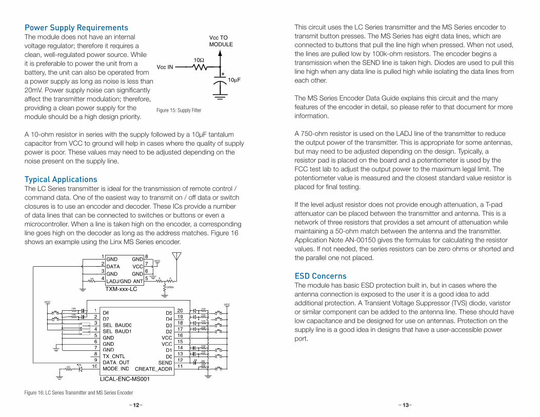
Typical ApplicationsThe LC Series transmitter is ideal for the transmission of remote control / command data. One of the easiest way to transmit on / off data or switch closures is to use an encoder and decoder. These ICs provide a number of data lines that can be connected to switches or buttons or even a microcontroller. When a line is taken high on the encoder, a corresponding line goes high on the decoder as long as the address matches. Figure 16 shows an example using the Linx MS Series encoder.
100k
100k
220
100k
100k
100k
100k
100k
100k
100k
LICAL-ENC-MS001
D6D7SEL_BAUD0SEL_BAUD1GNDGNDGNDTX_CNTLDATA_OUTMODE_IND
D5D4D3D2
VCCVCC
D1D0
SENDCREATE_ADDR
123456789
10 11121314151617181920
220
TXM-xxx-LC
1
2
3
4 5
6
7
8GND
VCC
GND
ANT
GND
DATA
GND
LADJ/GND750 0 0
OPEN
This circuit uses the LC Series transmitter and the MS Series encoder to transmit button presses. The MS Series has eight data lines, which are connected to buttons that pull the line high when pressed. When not used, the lines are pulled low by 100k-ohm resistors. The encoder begins a transmission when the SEND line is taken high. Diodes are used to pull this line high when any data line is pulled high while isolating the data lines from each other.
The MS Series Encoder Data Guide explains this circuit and the many features of the encoder in detail, so please refer to that document for more information.
A 750-ohm resistor is used on the LADJ line of the transmitter to reduce the output power of the transmitter. This is appropriate for some antennas, but may need to be adjusted depending on the design. Typically, a resistor pad is placed on the board and a potentiometer is used by the FCC test lab to adjust the output power to the maximum legal limit. The potentiometer value is measured and the closest standard value resistor is placed for final testing.
If the level adjust resistor does not provide enough attenuation, a T-pad attenuator can be placed between the transmitter and antenna. This is a network of three resistors that provides a set amount of attenuation while maintaining a 50-ohm match between the antenna and the transmitter. Application Note AN-00150 gives the formulas for calculating the resistor values. If not needed, the series resistors can be zero ohms or shorted and the parallel one not placed.
ESD ConcernsThe module has basic ESD protection built in, but in cases where the antenna connection is exposed to the user it is a good idea to add additional protection. A Transient Voltage Suppressor (TVS) diode, varistor or similar component can be added to the antenna line. These should have low capacitance and be designed for use on antennas. Protection on the supply line is a good idea in designs that have a user-accessible power port.
Figure 16: LC Series Transmitter and MS Series Encoder
+
10Ω
10µF
Vcc IN
Vcc TOMODULE
Figure 15: Supply Filter
– – – –14 15
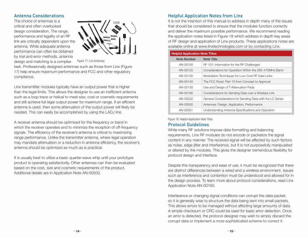
Antenna ConsiderationsThe choice of antennas is a critical and often overlooked design consideration. The range, performance and legality of an RF link are critically dependent upon the antenna. While adequate antenna performance can often be obtained by trial and error methods, antenna design and matching is a complex task. Professionally designed antennas such as those from Linx (Figure 17) help ensure maximum performance and FCC and other regulatory compliance.
Linx transmitter modules typically have an output power that is higher than the legal limits. This allows the designer to use an inefficient antenna such as a loop trace or helical to meet size, cost or cosmetic requirements and still achieve full legal output power for maximum range. If an efficient antenna is used, then some attenuation of the output power will likely be needed. This can easily be accomplished by using the LADJ line.
A receiver antenna should be optimized for the frequency or band in which the receiver operates and to minimize the reception of off-frequency signals. The efficiency of the receiver’s antenna is critical to maximizing range performance. Unlike the transmitter antenna, where legal operation may mandate attenuation or a reduction in antenna efficiency, the receiver’s antenna should be optimized as much as is practical.
It is usually best to utilize a basic quarter-wave whip until your prototype product is operating satisfactorily. Other antennas can then be evaluated based on the cost, size and cosmetic requirements of the product. Additional details are in Application Note AN-00500.
Figure 17: Linx Antennas
Helpful Application Notes from LinxIt is not the intention of this manual to address in depth many of the issues that should be considered to ensure that the modules function correctly and deliver the maximum possible performance. We recommend reading the application notes listed in Figure 18 which address in depth key areas of RF design and application of Linx products. These applications notes are available online at www.linxtechnologies.com or by contacting Linx.
Protocol GuidelinesWhile many RF solutions impose data formatting and balancing requirements, Linx RF modules do not encode or packetize the signal content in any manner. The received signal will be affected by such factors as noise, edge jitter and interference, but it is not purposefully manipulated or altered by the modules. This gives the designer tremendous flexibility for protocol design and interface.
Despite this transparency and ease of use, it must be recognized that there are distinct differences between a wired and a wireless environment. Issues such as interference and contention must be understood and allowed for in the design process. To learn more about protocol considerations, read Linx Application Note AN-00160.
Interference or changing signal conditions can corrupt the data packet, so it is generally wise to structure the data being sent into small packets. This allows errors to be managed without affecting large amounts of data. A simple checksum or CRC could be used for basic error detection. Once an error is detected, the protocol designer may wish to simply discard the corrupt data or implement a more sophisticated scheme to correct it.
Helpful Application Note Titles
Note Number Note Title
AN-00100 RF 101: Information for the RF Challenged
AN-00125 Considerations for Operation Within the 260–470MHz Band
AN-00130 Modulation Techniques for Low-Cost RF Data Links
AN-00140 The FCC Road: Part 15 from Concept to Approval
AN-00150 Use and Design of T-Attenuation Pads
AN-00160 Considerations for Sending Data over a Wireless Link
AN-00232 General Considerations for Sending Data with the LC Series
AN-00500 Antennas: Design, Application, Performance
AN-00501 Understanding Antenna Specifications and Operation
Figure 18: Helpful Application Note Titles
– – – –16 17
Interference ConsiderationsThe RF spectrum is crowded and the potential for conflict with unwanted sources of RF is very real. While all RF products are at risk from interference, its effects can be minimized by better understanding its characteristics.
Interference may come from internal or external sources. The first step is to eliminate interference from noise sources on the board. This means paying careful attention to layout, grounding, filtering and bypassing in order to eliminate all radiated and conducted interference paths. For many products, this is straightforward; however, products containing components such as switching power supplies, motors, crystals and other potential sources of noise must be approached with care. Comparing your own design with a Linx evaluation board can help to determine if and at what level design-specific interference is present.
External interference can manifest itself in a variety of ways. Low-level interference produces noise and hashing on the output and reduces the link’s overall range.
High-level interference is caused by nearby products sharing the same frequency or from near-band high-power devices. It can even come from your own products if more than one transmitter is active in the same area. It is important to remember that only one transmitter at a time can occupy a frequency, regardless of the coding of the transmitted signal. This type of interference is less common than those mentioned previously, but in severe cases it can prevent all useful function of the affected device.
Although technically not interference, multipath is also a factor to be understood. Multipath is a term used to refer to the signal cancellation effects that occur when RF waves arrive at the receiver in different phase relationships. This effect is a particularly significant factor in interior environments where objects provide many different signal reflection paths. Multipath cancellation results in lowered signal levels at the receiver and shorter useful distances for the link.
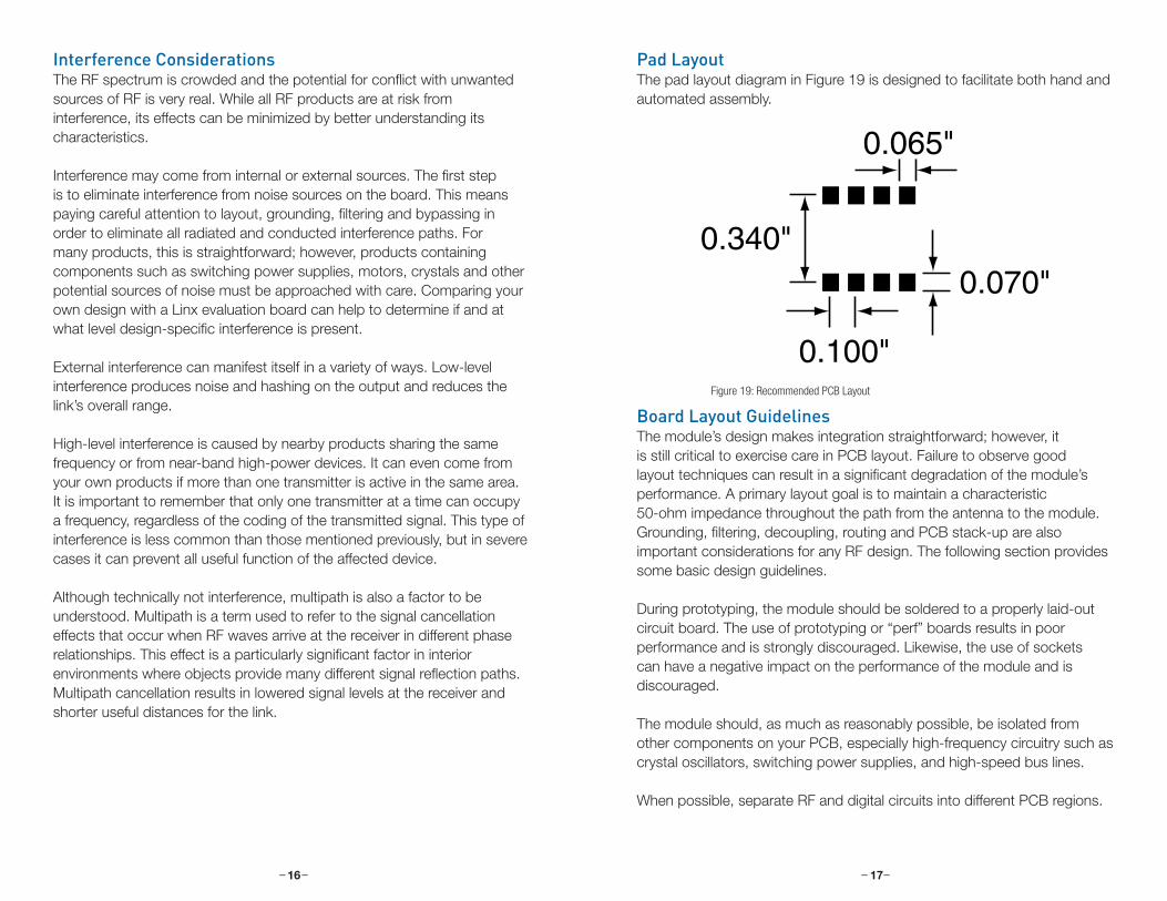
Pad LayoutThe pad layout diagram in Figure 19 is designed to facilitate both hand and automated assembly.
Board Layout GuidelinesThe module’s design makes integration straightforward; however, it is still critical to exercise care in PCB layout. Failure to observe good layout techniques can result in a significant degradation of the module’s performance. A primary layout goal is to maintain a characteristic 50-ohm impedance throughout the path from the antenna to the module. Grounding, filtering, decoupling, routing and PCB stack-up are also important considerations for any RF design. The following section provides some basic design guidelines.
During prototyping, the module should be soldered to a properly laid-out circuit board. The use of prototyping or “perf” boards results in poor performance and is strongly discouraged. Likewise, the use of sockets can have a negative impact on the performance of the module and is discouraged.
The module should, as much as reasonably possible, be isolated from other components on your PCB, especially high-frequency circuitry such as crystal oscillators, switching power supplies, and high-speed bus lines.
When possible, separate RF and digital circuits into different PCB regions.
Figure 19: Recommended PCB Layout
0.100"
0.070"
0.065"
0.340"
– – – –18 19
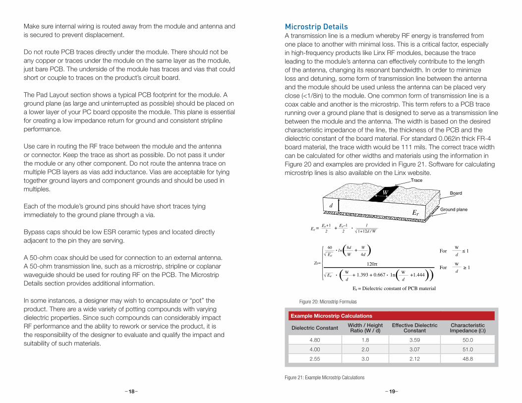
Microstrip DetailsA transmission line is a medium whereby RF energy is transferred from one place to another with minimal loss. This is a critical factor, especially in high-frequency products like Linx RF modules, because the trace leading to the module’s antenna can effectively contribute to the length of the antenna, changing its resonant bandwidth. In order to minimize loss and detuning, some form of transmission line between the antenna and the module should be used unless the antenna can be placed very close (<1/8in) to the module. One common form of transmission line is a coax cable and another is the microstrip. This term refers to a PCB trace running over a ground plane that is designed to serve as a transmission line between the module and the antenna. The width is based on the desired characteristic impedance of the line, the thickness of the PCB and the dielectric constant of the board material. For standard 0.062in thick FR-4 board material, the trace width would be 111 mils. The correct trace width can be calculated for other widths and materials using the information in Figure 20 and examples are provided in Figure 21. Software for calculating microstrip lines is also available on the Linx website.
Trace
Board
Ground plane
Figure 20: Microstrip Formulas
Example Microstrip Calculations
Dielectric Constant Width / Height Ratio (W / d)
Effective Dielectric Constant
Characteristic Impedance (Ω)
4.80 1.8 3.59 50.0
4.00 2.0 3.07 51.0
2.55 3.0 2.12 48.8
Figure 21: Example Microstrip Calculations
Make sure internal wiring is routed away from the module and antenna and is secured to prevent displacement.
Do not route PCB traces directly under the module. There should not be any copper or traces under the module on the same layer as the module, just bare PCB. The underside of the module has traces and vias that could short or couple to traces on the product’s circuit board.
The Pad Layout section shows a typical PCB footprint for the module. A ground plane (as large and uninterrupted as possible) should be placed on a lower layer of your PC board opposite the module. This plane is essential for creating a low impedance return for ground and consistent stripline performance.
Use care in routing the RF trace between the module and the antenna or connector. Keep the trace as short as possible. Do not pass it under the module or any other component. Do not route the antenna trace on multiple PCB layers as vias add inductance. Vias are acceptable for tying together ground layers and component grounds and should be used in multiples.
Each of the module’s ground pins should have short traces tying immediately to the ground plane through a via.
Bypass caps should be low ESR ceramic types and located directly adjacent to the pin they are serving.
A 50-ohm coax should be used for connection to an external antenna. A 50-ohm transmission line, such as a microstrip, stripline or coplanar waveguide should be used for routing RF on the PCB. The Microstrip Details section provides additional information.
In some instances, a designer may wish to encapsulate or “pot” the product. There are a wide variety of potting compounds with varying dielectric properties. Since such compounds can considerably impact RF performance and the ability to rework or service the product, it is the responsibility of the designer to evaluate and qualify the impact and suitability of such materials.
– – – –20 21
Production GuidelinesThe module is housed in a hybrid SMD package that supports hand and automated assembly techniques. Since the modules contain discrete components internally, the assembly procedures are critical to ensuring the reliable function of the modules. The following procedures should be reviewed with and practiced by all assembly personnel.
Hand AssemblyPads located on the bottom of the module are the primary mounting surface (Figure 22). Since these pads are inaccessible during mounting, castellations that run up the side of the module have been provided to facilitate solder wicking to the module’s underside. This allows for very quick hand soldering for prototyping and small volume production. If the recommended pad guidelines have been followed, the pads will protrude slightly past the edge of the module. Use a fine soldering tip to heat the board pad and the castellation, then introduce solder to the pad at the module’s edge. The solder will wick underneath the module, providing reliable attachment. Tack one module corner first and then work around the device, taking care not to exceed the times in Figure 23.
Automated AssemblyFor high-volume assembly, the modules are generally auto-placed. The modules have been designed to maintain compatibility with reflow processing techniques; however, due to their hybrid nature, certain aspects of the assembly process are far more critical than for other component types. Following are brief discussions of the three primary areas where caution must be observed.
CastellationsPCB Pads
Soldering IronTip
Solder
Figure 22: Soldering Technique
Warning: Pay attention to the absolute maximum solder times.
Figure 23: Absolute Maximum Solder Times
Absolute Maximum Solder Times
Hand Solder Temperature: +427ºC for 10 seconds for lead-free alloys
Reflow Oven: +255ºC max (see Figure 24)
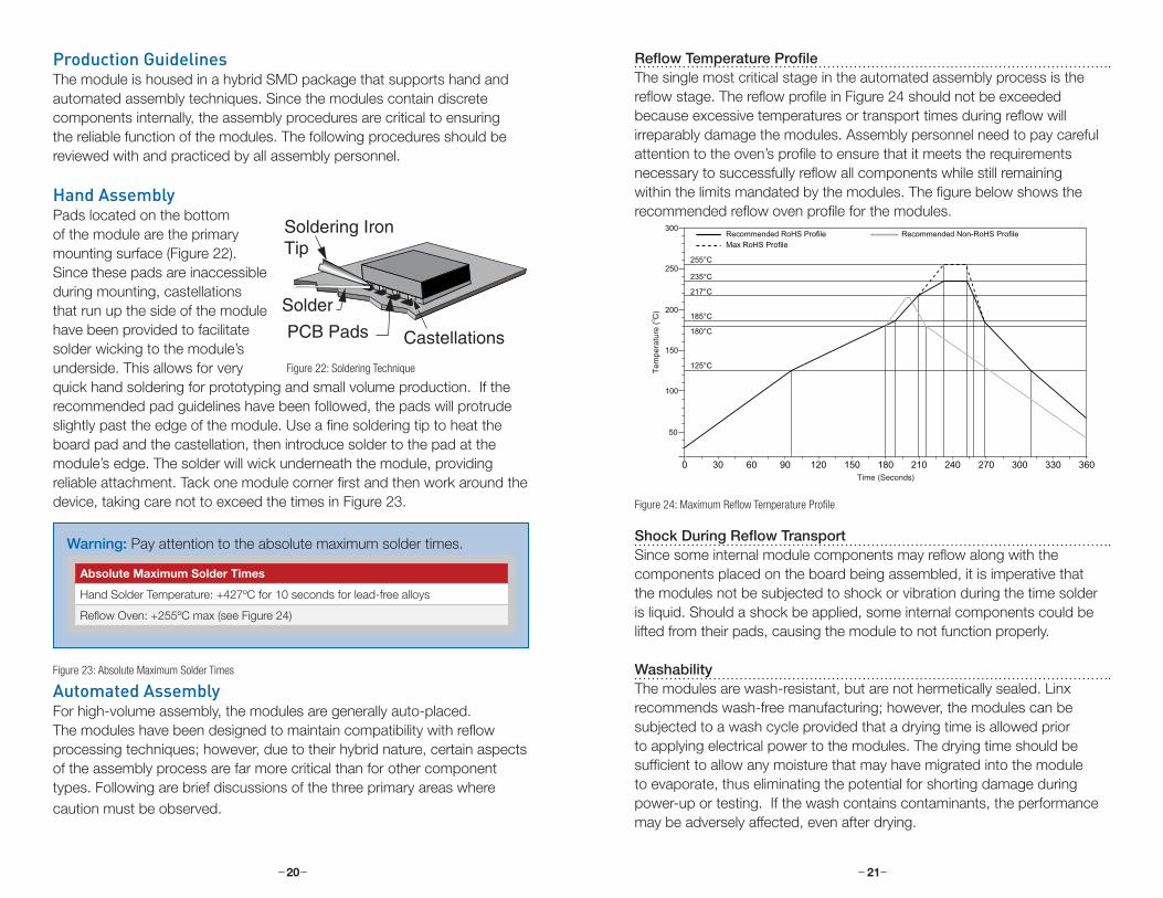
Reflow Temperature ProfileThe single most critical stage in the automated assembly process is the reflow stage. The reflow profile in Figure 24 should not be exceeded because excessive temperatures or transport times during reflow will irreparably damage the modules. Assembly personnel need to pay careful attention to the oven’s profile to ensure that it meets the requirements necessary to successfully reflow all components while still remaining within the limits mandated by the modules. The figure below shows the recommended reflow oven profile for the modules.
Shock During Reflow TransportSince some internal module components may reflow along with the components placed on the board being assembled, it is imperative that the modules not be subjected to shock or vibration during the time solder is liquid. Should a shock be applied, some internal components could be lifted from their pads, causing the module to not function properly.
WashabilityThe modules are wash-resistant, but are not hermetically sealed. Linx recommends wash-free manufacturing; however, the modules can be subjected to a wash cycle provided that a drying time is allowed prior to applying electrical power to the modules. The drying time should be sufficient to allow any moisture that may have migrated into the module to evaporate, thus eliminating the potential for shorting damage during power-up or testing. If the wash contains contaminants, the performance may be adversely affected, even after drying.
125°C
185°C
217°C
255°C
235°C
60 12030 150 180 210 240 270 300 330 3600 90
50
100
150
200
250
300Recommended RoHS ProfileMax RoHS Profile
Recommended Non-RoHS Profile
180°C
Tem
pera
ture
(o C
)
Time (Seconds)
Figure 24: Maximum Reflow Temperature Profile
– – – –22 23
General Antenna RulesThe following general rules should help in maximizing antenna performance.
1. Proximity to objects such as a user’s hand, body or metal objects will cause an antenna to detune. For this reason, the antenna shaft and tip should be positioned as far away from such objects as possible.
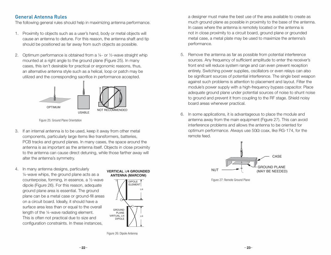
2. Optimum performance is obtained from a ¼- or ½-wave straight whip mounted at a right angle to the ground plane (Figure 25). In many cases, this isn’t desirable for practical or ergonomic reasons, thus, an alternative antenna style such as a helical, loop or patch may be utilized and the corresponding sacrifice in performance accepted.
3. If an internal antenna is to be used, keep it away from other metal components, particularly large items like transformers, batteries, PCB tracks and ground planes. In many cases, the space around the antenna is as important as the antenna itself. Objects in close proximity to the antenna can cause direct detuning, while those farther away will alter the antenna’s symmetry.
4. In many antenna designs, particularly ¼-wave whips, the ground plane acts as a counterpoise, forming, in essence, a ½-wave dipole (Figure 26). For this reason, adequate ground plane area is essential. The ground plane can be a metal case or ground-fill areas on a circuit board. Ideally, it should have a surface area less than or equal to the overall length of the ¼-wave radiating element. This is often not practical due to size and configuration constraints. In these instances,
OPTIMUM
USABLENOT RECOMMENDED
NUTGROUND PLANE
(MAY BE NEEDED)
CASE
Figure 25: Ground Plane Orientation
I
E DIPOLEELEMENT
GROUNDPLANE
VIRTUAL λ/4DIPOLE
λ/4
λ/4
VERTICAL λ/4 GROUNDEDANTENNA (MARCONI)
a designer must make the best use of the area available to create as much ground plane as possible in proximity to the base of the antenna. In cases where the antenna is remotely located or the antenna is not in close proximity to a circuit board, ground plane or grounded metal case, a metal plate may be used to maximize the antenna’s performance.
5. Remove the antenna as far as possible from potential interference sources. Any frequency of sufficient amplitude to enter the receiver’s front end will reduce system range and can even prevent reception entirely. Switching power supplies, oscillators or even relays can also be significant sources of potential interference. The single best weapon against such problems is attention to placement and layout. Filter the module’s power supply with a high-frequency bypass capacitor. Place adequate ground plane under potential sources of noise to shunt noise to ground and prevent it from coupling to the RF stage. Shield noisy board areas whenever practical.
6. In some applications, it is advantageous to place the module and antenna away from the main equipment (Figure 27). This can avoid interference problems and allows the antenna to be oriented for optimum performance. Always use 50Ω coax, like RG-174, for the remote feed.
OPTIMUM
USABLENOT RECOMMENDED
NUTGROUND PLANE
(MAY BE NEEDED)
CASE
Figure 27: Remote Ground Plane
Figure 26: Dipole Antenna
– – – –24 25
Common Antenna StylesThere are hundreds of antenna styles and variations that can be employed with Linx RF modules. Following is a brief discussion of the styles most commonly utilized. Additional antenna information can be found in Linx Application Notes AN-00100, AN-00140, AN-00500 and AN-00501. Linx antennas and connectors offer outstanding performance at a low price.
Whip Style A whip style antenna (Figure 28) provides outstanding overall performance and stability. A low-cost whip can be easily fabricated from a wire or rod, but most designers opt for the consistent performance and cosmetic appeal of a professionally-made model. To meet this need, Linx offers a wide variety of straight and reduced height whip style antennas in permanent and connectorized mounting styles.
The wavelength of the operational frequency determines an antenna’s overall length. Since a full wavelength is often quite long, a partial ½- or ¼-wave antenna is normally employed. Its size and natural radiation resistance make it well matched to Linx modules. The proper length for a straight ¼-wave can be easily determined using the formula in Figure 29. It is also possible to reduce the overall height of the antenna by using a helical winding. This reduces the antenna’s bandwidth but is a great way to minimize the antenna’s physical size for compact applications. This also means that the physical appearance is not always an indicator of the antenna’s frequency.
Specialty StylesLinx offers a wide variety of specialized antenna styles (Figure 30). Many of these styles utilize helical elements to reduce the overall antenna size while maintaining reasonable performance. A helical antenna’s bandwidth is often quite narrow and the antenna can detune in proximity to other objects, so care must be exercised in layout and placement.
L =234
F MHz
Figure 28: Whip Style Antennas
Figure 29: L = length in feet of quarter-wave lengthF = operating frequency in megahertz
Figure 30: Specialty Style Antennas
Loop StyleA loop or trace style antenna is normally printed directly on a product’s PCB (Figure 31). This makes it the most cost-effective of antenna styles. The element can be made self-resonant or externally resonated with discrete components, but its actual layout is usually product specific. Despite the cost advantages, loop style antennas are generally inefficient and useful only for short range applications. They are also very sensitive to changes in layout and PCB dielectric, which can cause consistency issues during production. In addition, printed styles are difficult to engineer, requiring the use of expensive equipment including a network analyzer. An improperly designed loop will have a high VSWR at the desired frequency which can cause instability in the RF stage.
Linx offers low-cost planar (Figure 32) and chip antennas that mount directly to a product’s PCB. These tiny antennas do not require testing and provide excellent performance despite their small size. They offer a preferable alternative to the often problematic “printed” antenna.
Figure 31: Loop or Trace Antenna
Figure 32: SP Series “Splatch” and uSP “MicroSplatch” Antennas
– – – –26 27
Regulatory Considerations
When working with RF, a clear distinction must be made between what is technically possible and what is legally acceptable in the country where operation is intended. Many manufacturers have avoided incorporating RF into their products as a result of uncertainty and even fear of the approval and certification process. Here at Linx, our desire is not only to expedite the design process, but also to assist you in achieving a clear idea of what is involved in obtaining the necessary approvals to legally market a completed product.
For information about regulatory approval, read AN-00142 on the Linx website or call Linx. Linx designs products with worldwide regulatory approval in mind.
In the United States, the approval process is actually quite straightforward. The regulations governing RF devices and the enforcement of them are the responsibility of the Federal Communications Commission (FCC). The regulations are contained in Title 47 of the United States Code of Federal Regulations (CFR). Title 47 is made up of numerous volumes; however, all regulations applicable to this module are contained in Volume 0-19. It is strongly recommended that a copy be obtained from the FCC’s website, the Government Printing Office in Washington or from your local government bookstore. Excerpts of applicable sections are included with Linx evaluation kits or may be obtained from the Linx Technologies website, www.linxtechnologies.com. In brief, these rules require that any device that intentionally radiates RF energy be approved, that is, tested for compliance and issued a unique identification number. This is a relatively painless process. Final compliance testing is performed by one of the many independent testing laboratories across the country. Many labs can also provide other certifications that the product may require at the same time, such as UL, CLASS A / B, etc. Once the completed product has passed, an ID number is issued that is to be clearly placed on each product manufactured.
Note: Linx RF modules are designed as component devices that require external components to function. The purchaser understands that additional approvals may be required prior to the sale or operation of the device, and agrees to utilize the component in keeping with all laws governing its use in the country of operation.
Questions regarding interpretations of the Part 2 and Part 15 rules or the measurement procedures used to test intentional radiators such as Linx RF modules for compliance with the technical standards of Part 15 should be addressed to:
Federal Communications Commission Equipment Authorization Division Customer Service Branch, MS 1300F2 7435 Oakland Mills Road Columbia, MD, US 21046 Phone: + 1 301 725 585 | Fax: + 1 301 344 2050 Email: [email protected]
ETSI Secretaria650, Route des Lucioles06921 Sophia-Antipolis CedexFRANCEPhone: +33 (0)4 92 94 42 00 Fax: +33 (0)4 93 65 47 16
International approvals are slightly more complex, although Linx modules are designed to allow all international standards to be met. If the end product is to be exported to other countries, contact Linx to determine the specific suitability of the module to the application.
All Linx modules are designed with the approval process in mind and thus much of the frustration that is typically experienced with a discrete design is eliminated. Approval is still dependent on many factors, such as the choice of antennas, correct use of the frequency selected and physical packaging. While some extra cost and design effort are required to address these issues, the additional usefulness and profitability added to a product by RF makes the effort more than worthwhile.
Linx Technologies
159 Ort Lane
Merlin, OR, US 97532
3090 Sterling Circle, Suite 200
Boulder, CO 80301
Phone: +1 541 471 6256
Fax: +1 541 471 6251
www.linxtechnologies.com
DisclaimerLinx Technologies is continually striving to improve the quality and function of its products. For this reason, we reserve the right to make changes to our products without notice. The information contained in this Data Guide is believed to be accurate as of the time of publication. Specifications are based on representative lot samples. Values may vary from lot-to-lot and are not guaranteed. “Typical” parameters can and do vary over lots and application. Linx Technologies makes no guarantee, warranty, or representation regarding the suitability of any product for use in any specific application. It is Customer’s responsibility to verify the suitability of the part for the intended application. At Customer’s request, Linx Technologies may provide advice and assistance in designing systems and remote control devices that employ Linx Technologies RF products, but responsibility for the ultimate design and use of any such systems and devices remains entirely with Customer and/or user of the RF products.
LINX TECHNOLOGIES DISCLAIMS ANY AND ALL WARRANTIES OF MERCHANTABILITY AND FITNESS FOR A PARTICULAR PURPOSE. IN NO EVENT SHALL LINX TECHNOLOGIES BE LIABLE FOR ANY CUSTOMER’S OR USER’S INCIDENTAL OR CONSEQUENTIAL DAMAGES ARISING OUT OF OR RELATED TO THE DESIGN OR USE OF A REMOTE CONTROL SYSTEM OR DEVICE EMPLOYING LINX TECHNOLOGIES RF PRODUCTS OR FOR ANY OTHER BREACH OF CONTRACT BY LINX TECHNOLOGIES. CUSTOMER AND/OR USER ASSUME ALL RISKS OF DEATH, BODILY INJURIES, OR PROPERTY DAMAGE ARISING OUT OF OR RELATED TO THE USE OF LINX TECHNOLOGIES RF PRODUCTS, INCLUDING WITH RESPECT TO ANY SERVICES PROVIDED BY LINX RELATED TO THE USE OF LINX TECHNOLOGIES RF PRODUCTS. LINX TECHNOLOGIES SHALL NOT BE LIABLE UNDER ANY CIRCUMSTANCES FOR A CUSTOMER’S, USER’S, OR OTHER PERSON’S DEATH, BODILY INJURY, OR PROPERTY DAMAGE ARISING OUT OF OR RELATED TO THE DESIGN OR USE OF A REMOTE CONTROL SYSTEM OR DEVICE EMPLOYING LINX TECHNOLOGIES RF PRODUCTS.
The limitations on Linx Technologies’ liability are applicable to any and all claims or theories of recovery asserted by Customer, including, without limitation, breach of contract, breach of warranty, strict liability, or negligence. Customer assumes all liability (including, without limitation, liability for injury to person or property, economic loss, or business interruption) for all claims, including claims from third parties, arising from the use of the Products. Under no conditions will Linx Technologies be responsible for losses arising from the use or failure of the device in any application, other than the repair, replacement, or refund limited to the original product purchase price. Devices described in this publication may contain proprietary, patented, or copyrighted techniques, components, or materials.
© 2014 Linx Technologies. All rights reserved.
The stylized Linx logo, Wireless Made Simple, CipherLinx, WiSE and the stylized CL logo are trademarks of Linx Technologies.