Embed Size (px)
Citation preview
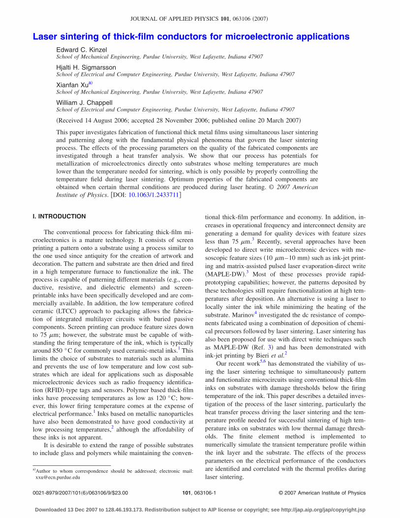
Laser sintering of thick-film conductors for microelectronic applicationsEdward C. KinzelSchool of Mechanical Engineering, Purdue University, West Lafayette, Indiana 47907
Hjalti H. SigmarssonSchool of Electrical and Computer Engineering, Purdue University, West Lafayette, Indiana 47907
Xianfan Xua�
School of Mechanical Engineering, Purdue University, West Lafayette, Indiana 47907
William J. ChappellSchool of Electrical and Computer Engineering, Purdue University, West Lafayette, Indiana 47907
�Received 14 August 2006; accepted 28 November 2006; published online 20 March 2007�
This paper investigates fabrication of functional thick metal films using simultaneous laser sinteringand patterning along with the fundamental physical phenomena that govern the laser sinteringprocess. The effects of the processing parameters on the quality of the fabricated components areinvestigated through a heat transfer analysis. We show that our process has potentials formetallization of microelectronics directly onto substrates whose melting temperatures are muchlower than the temperature needed for sintering, which is only possible by properly controlling thetemperature field during laser sintering. Optimum properties of the fabricated components areobtained when certain thermal conditions are produced during laser heating. © 2007 AmericanInstitute of Physics. �DOI: 10.1063/1.2433711�
I. INTRODUCTION
The conventional process for fabricating thick-film mi-croelectronics is a mature technology. It consists of screenprinting a pattern onto a substrate using a process similar tothe one used since antiquity for the creation of artwork anddecoration. The pattern and substrate are then dried and firedin a high temperature furnace to functionalize the ink. Theprocess is capable of patterning different materials �e.g., con-ductive, resistive, and dielectric elements� and screen-printable inks have been specifically developed and are com-mercially available. In addition, the low temperature cofiredceramic �LTCC� approach to packaging allows the fabrica-tion of integrated multilayer circuits with buried passivecomponents. Screen printing can produce feature sizes downto 75 �m; however, the substrate must be capable of with-standing the firing temperature of the ink, which is typicallyaround 850 °C for commonly used ceramic-metal inks.1 Thislimits the choice of substrates to materials such as aluminaand prevents the use of low temperature and low cost sub-strates which are ideal for applications such as disposablemicroelectronic devices such as radio frequency identifica-tion �RFID�-type tags and sensors. Polymer based thick-filminks have processing temperatures as low as 120 °C; how-ever, this lower firing temperature comes at the expense ofelectrical performance.1 Inks based on metallic nanoparticleshave also been demonstrated to have good conductivity atlow processing temperatures,2 although the affordability ofthese inks is not apparent.
It is desirable to extend the range of possible substratesto include glass and polymers while maintaining the conven-
tional thick-film performance and economy. In addition, in-creases in operational frequency and interconnect density aregenerating a demand for quality devices with feature sizesless than 75 �m.3 Recently, several approaches have beendeveloped to direct write microelectronic devices with me-soscopic feature sizes �10 �m–10 mm� such as ink-jet print-ing and matrix-assisted pulsed laser evaporation-direct write�MAPLE-DW�.3 Most of these processes provide rapid-prototyping capabilities; however, the patterns deposited bythese technologies still require functionalization at high tem-peratures after deposition. An alternative is using a laser tolocally sinter the ink while minimizing the heating of thesubstrate. Marinov4 investigated the dc resistance of compo-nents fabricated using a combination of deposition of chemi-cal precursors followed by laser sintering. Laser sintering hasalso been proposed for use with direct write techniques suchas MAPLE-DW �Ref. 3� and has been demonstrated withink-jet printing by Bieri et al.2
Our recent work5,6 has demonstrated the viability of us-ing the laser sintering technique to simultaneously patternand functionalize microcircuits using conventional thick-filminks on substrates with damage thresholds below the firingtemperature of the ink. This paper describes a detailed inves-tigation of the process of the laser sintering, particularly theheat transfer process driving the laser sintering and the tem-perature profile needed for successful sintering of high tem-perature inks on substrates with low thermal damage thresh-olds. The finite element method is implemented tonumerically simulate the transient temperature profile withinthe ink layer and the substrate. The effects of the processparameters on the electrical performance of the conductorsare identified and correlated with the thermal profiles duringlaser sintering.
a�Author to whom correspondence should be addressed; electronic mail:[email protected]
JOURNAL OF APPLIED PHYSICS 101, 063106 �2007�
0021-8979/2007/101�6�/063106/9/$23.00 © 2007 American Institute of Physics101, 063106-1
Downloaded 13 Dec 2007 to 128.46.193.173. Redistribution subject to AIP license or copyright; see http://jap.aip.org/jap/copyright.jsp
II. EXPERIMENT
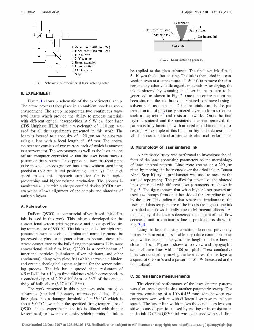
Figure 1 shows a schematic of the experimental setup.The entire process takes place in an ambient nonclean roomenvironment. The setup incorporates two continuous wave�cw� lasers which provide the ability to process materialswith different optical absorptivities. A 9 W cw fiber laser�JDS Uniphase IFL9� with a wavelength of 1.10 �m wasused for all the experiments presented in this work. Thebeam is focused to a spot size of �20 �m on the substrateusing a lens with a focal length of 165 mm. The opticalx-y scanner consists of two mirrors each of which is attachedto a servomotor. The servomotors as well as the laser on andoff are computer controlled so that the laser beam traces apattern on the substrate. This approach allows the focal pointto be moved at speeds greater than 1 m/s without sacrificingprecision ��2 �m lateral positioning accuracy�. The highspeed makes this approach attractive for both rapid-prototyping and higher-volume production. The process ismonitored in situ with a charge coupled device �CCD� cam-era which allows alignment of the sample and sintering ofmultiple layers.
A. Fabrication
DuPont QS300, a commercial silver based thick-filmink, is used in this work. This ink was developed for theconventional screen printing process and has a specified fir-ing temperature of 850 °C. The ink is intended for high tem-perature substrates such as alumina and normally cannot beprocessed on glass or polymer substrates because these sub-strates cannot survive the bulk firing temperatures. Like mostconventional thick-film inks, QS300 is a combination offunctional particles �submicron silver, platinum, and otherconductors�, along with glass frit �which serves as a binder�and organic rheological agents adjusted for the screen print-ing process. The ink has a quoted sheet resistance of4.5 m� /� for a 10 �m fired thickness which corresponds toa conductivity � of 2.22�107 S/m or 36% of the conduc-tivity of bulk silver �6.17�107 S/m�.
The work presented in this paper uses soda-lime glasssubstrates �standard laboratory microscope slides�. Soda-lime glass has a damage threshold of �550 °C which isabout 300 °C lower than the specified firing temperature ofQS300. In the experiments, the ink is diluted with thinner��-terpineol� to lower its viscosity which permits the ink to
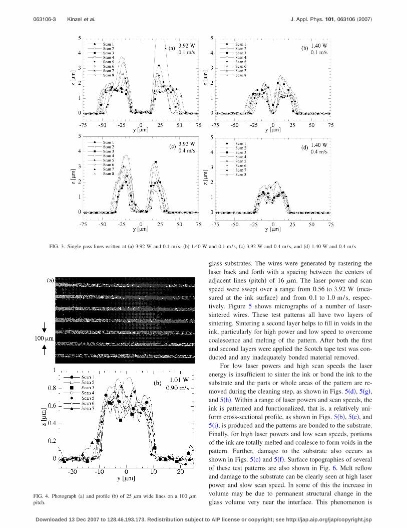
be applied to the glass substrate. The final wet ink film is5–10 �m thick after coating. The ink is then dried in a con-vection oven at a temperature of 150 °C to remove the thin-ner and any other volatile organic materials. After drying, theink is sintered by scanning the laser in the pattern to begenerated, as shown in Fig. 2. Once the entire pattern hasbeen sintered, the ink that is not sintered is removed using asolvent such as methanol. Other materials can also be pat-terned on top of previously sintered layers to form structuressuch as capacitors7 and resistor networks. Once the finallayer is sintered and the unsintered material removed, thepattern is fully functional with no need of additional postpro-cessing. An example of this functionality is the dc resistancewhich is measured to characterize its electrical performance.
B. Morphology of laser sintered ink
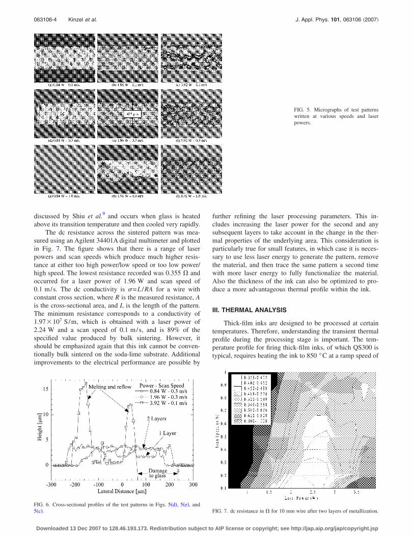
A parametric study was performed to investigate the ef-fects of the laser processing parameters on the morphologyof laser sintered patterns. Lines were created on a 200 �mpitch by moving the laser once over the dried ink. A TencorAlpha-Step IQ stylus profilometer was used to measure thesurface topography. The profiles for several of the sinteredlines generated with different laser parameters are shown inFig. 3. The figure shows that when higher laser powers areused, two bumps form on either side of the centerline tracedby the laser. This indicates that where the irradiance of thelaser �and thus temperature of the ink� is the highest, the inkis melted and flows laterally due to Marangoni effects.8 Asthe intensity of the laser is decreased the amount of melt flowdecreases until a continuous line is produced, as shown inFig. 3�d�.
Using the laser focusing condition described previously,further experimentation was able to produce continuous lineswith widths less than 25 �m. The height of these lines isclose to 1 �m. Figure 4 shows a top view and topographicscans of these lines with a 100 �m pitch. These conductivelines were created by moving the laser across the ink layer ata speed of 0.90 m/s and a power of 1.01 W �measured at theink surface�.
C. dc resistance measurements
The electrical performance of the laser sintered patternswas also investigated using another parametric sweep. Testpatterns consisting of a 10�0.425 mm2 wire between twoconnectors were written with different laser powers and scanspeeds. The larger line width makes the conductors less sen-sitive to any disparities caused by coating or inconsistenciesin the ink. DuPont QS300 ink was again used with soda-lime
FIG. 1. Schematic of experimental laser sintering setup.
FIG. 2. Laser sintering process.
063106-2 Kinzel et al. J. Appl. Phys. 101, 063106 �2007�
Downloaded 13 Dec 2007 to 128.46.193.173. Redistribution subject to AIP license or copyright; see http://jap.aip.org/jap/copyright.jsp
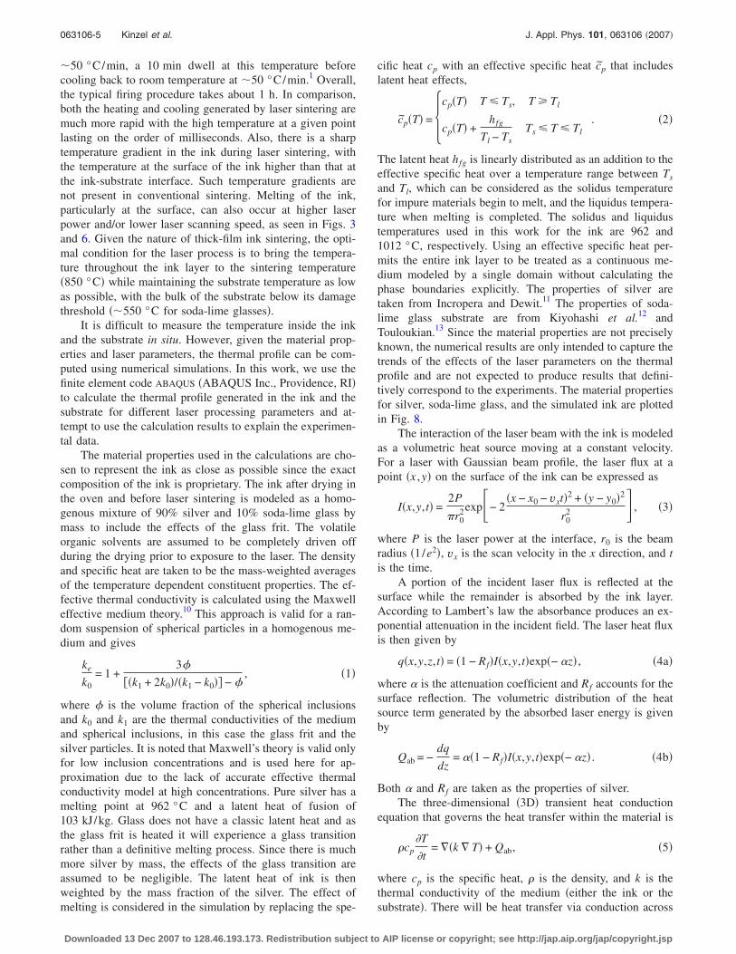
glass substrates. The wires were generated by rastering thelaser back and forth with a spacing between the centers ofadjacent lines �pitch� of 16 �m. The laser power and scanspeed were swept over a range from 0.56 to 3.92 W �mea-sured at the ink surface� and from 0.1 to 1.0 m/s, respec-tively. Figure 5 shows micrographs of a number of laser-sintered wires. These test patterns all have two layers ofsintering. Sintering a second layer helps to fill in voids in theink, particularly for high power and low speed to overcomecoalescence and melting of the pattern. After both the firstand second layers were applied the Scotch tape test was con-ducted and any inadequately bonded material removed.
For low laser powers and high scan speeds the laserenergy is insufficient to sinter the ink or bond the ink to thesubstrate and the parts or whole areas of the pattern are re-moved during the cleaning step, as shown in Figs. 5�d�, 5�g�,and 5�h�. Within a range of laser powers and scan speeds, theink is patterned and functionalized, that is, a relatively uni-form cross-sectional profile, as shown in Figs. 5�b�, 5�e�, and5�i�, is produced and the patterns are bonded to the substrate.Finally, for high laser powers and low scan speeds, portionsof the ink are totally melted and coalesce to form voids in thepattern. Further, damage to the substrate also occurs asshown in Figs. 5�c� and 5�f�. Surface topographies of severalof these test patterns are also shown in Fig. 6. Melt reflowand damage to the substrate can be clearly seen at high laserpower and slow scan speed. In some of this the increase involume may be due to permanent structural change in theglass volume very near the interface. This phenomenon is
FIG. 4. Photograph �a� and profile �b� of 25 �m wide lines on a 100 �mpitch.
FIG. 3. Single pass lines written at �a� 3.92 W and 0.1 m/s, �b� 1.40 W and 0.1 m/s, �c� 3.92 W and 0.4 m/s, and �d� 1.40 W and 0.4 m/s
063106-3 Kinzel et al. J. Appl. Phys. 101, 063106 �2007�
Downloaded 13 Dec 2007 to 128.46.193.173. Redistribution subject to AIP license or copyright; see http://jap.aip.org/jap/copyright.jsp
discussed by Shiu et al.9 and occurs when glass is heatedabove its transition temperature and then cooled very rapidly.
The dc resistance across the sintered pattern was mea-sured using an Agilent 34401A digital multimeter and plottedin Fig. 7. The figure shows that there is a range of laserpowers and scan speeds which produce much higher resis-tance at either too high power/low speed or too low power/high speed. The lowest resistance recorded was 0.355 � andoccurred for a laser power of 1.96 W and scan speed of0.1 m/s. The dc conductivity is �=L /RA for a wire withconstant cross section, where R is the measured resistance, Ais the cross-sectional area, and L is the length of the pattern.The minimum resistance corresponds to a conductivity of1.97�107 S/m, which is obtained with a laser power of2.24 W and a scan speed of 0.1 m/s, and is 89% of thespecified value produced by bulk sintering. However, itshould be emphasized again that this ink cannot be conven-tionally bulk sintered on the soda-lime substrate. Additionalimprovements to the electrical performance are possible by
further refining the laser processing parameters. This in-cludes increasing the laser power for the second and anysubsequent layers to take account in the change in the ther-mal properties of the underlying area. This consideration isparticularly true for small features, in which case it is neces-sary to use less laser energy to generate the pattern, removethe material, and then trace the same pattern a second timewith more laser energy to fully functionalize the material.Also the thickness of the ink can also be optimized to pro-duce a more advantageous thermal profile within the ink.
III. THERMAL ANALYSIS
Thick-film inks are designed to be processed at certaintemperatures. Therefore, understanding the transient thermalprofile during the processing stage is important. The tem-perature profile for firing thick-film inks, of which QS300 istypical, requires heating the ink to 850 °C at a ramp speed of
FIG. 5. Micrographs of test patternswritten at various speeds and laserpowers.
FIG. 6. Cross-sectional profiles of the test patterns in Figs. 5�d�, 5�e�, and5�c�. FIG. 7. dc resistance in � for 10 mm wire after two layers of metallization.
063106-4 Kinzel et al. J. Appl. Phys. 101, 063106 �2007�
Downloaded 13 Dec 2007 to 128.46.193.173. Redistribution subject to AIP license or copyright; see http://jap.aip.org/jap/copyright.jsp
�50 °C/min, a 10 min dwell at this temperature beforecooling back to room temperature at �50 °C/min.1 Overall,the typical firing procedure takes about 1 h. In comparison,both the heating and cooling generated by laser sintering aremuch more rapid with the high temperature at a given pointlasting on the order of milliseconds. Also, there is a sharptemperature gradient in the ink during laser sintering, withthe temperature at the surface of the ink higher than that atthe ink-substrate interface. Such temperature gradients arenot present in conventional sintering. Melting of the ink,particularly at the surface, can also occur at higher laserpower and/or lower laser scanning speed, as seen in Figs. 3and 6. Given the nature of thick-film ink sintering, the opti-mal condition for the laser process is to bring the tempera-ture throughout the ink layer to the sintering temperature�850 °C� while maintaining the substrate temperature as lowas possible, with the bulk of the substrate below its damagethreshold ��550 °C for soda-lime glasses�.
It is difficult to measure the temperature inside the inkand the substrate in situ. However, given the material prop-erties and laser parameters, the thermal profile can be com-puted using numerical simulations. In this work, we use thefinite element code ABAQUS �ABAQUS Inc., Providence, RI�to calculate the thermal profile generated in the ink and thesubstrate for different laser processing parameters and at-tempt to use the calculation results to explain the experimen-tal data.
The material properties used in the calculations are cho-sen to represent the ink as close as possible since the exactcomposition of the ink is proprietary. The ink after drying inthe oven and before laser sintering is modeled as a homo-genous mixture of 90% silver and 10% soda-lime glass bymass to include the effects of the glass frit. The volatileorganic solvents are assumed to be completely driven offduring the drying prior to exposure to the laser. The densityand specific heat are taken to be the mass-weighted averagesof the temperature dependent constituent properties. The ef-fective thermal conductivity is calculated using the Maxwelleffective medium theory.10 This approach is valid for a ran-dom suspension of spherical particles in a homogenous me-dium and gives
ke
k0= 1 +
3�
��k1 + 2k0�/�k1 − k0�� − �, �1�
where � is the volume fraction of the spherical inclusionsand k0 and k1 are the thermal conductivities of the mediumand spherical inclusions, in this case the glass frit and thesilver particles. It is noted that Maxwell’s theory is valid onlyfor low inclusion concentrations and is used here for ap-proximation due to the lack of accurate effective thermalconductivity model at high concentrations. Pure silver has amelting point at 962 °C and a latent heat of fusion of103 kJ/kg. Glass does not have a classic latent heat and asthe glass frit is heated it will experience a glass transitionrather than a definitive melting process. Since there is muchmore silver by mass, the effects of the glass transition areassumed to be negligible. The latent heat of ink is thenweighted by the mass fraction of the silver. The effect ofmelting is considered in the simulation by replacing the spe-
cific heat cp with an effective specific heat c̃p that includeslatent heat effects,
c̃p�T� = �cp�T� T � Ts, T Tl
cp�T� +hfg
Tl − TsTs � T � Tl � . �2�
The latent heat hfg is linearly distributed as an addition to theeffective specific heat over a temperature range between Ts
and Tl, which can be considered as the solidus temperaturefor impure materials begin to melt, and the liquidus tempera-ture when melting is completed. The solidus and liquidustemperatures used in this work for the ink are 962 and1012 °C, respectively. Using an effective specific heat per-mits the entire ink layer to be treated as a continuous me-dium modeled by a single domain without calculating thephase boundaries explicitly. The properties of silver aretaken from Incropera and Dewit.11 The properties of soda-lime glass substrate are from Kiyohashi et al.12 andTouloukian.13 Since the material properties are not preciselyknown, the numerical results are only intended to capture thetrends of the effects of the laser parameters on the thermalprofile and are not expected to produce results that defini-tively correspond to the experiments. The material propertiesfor silver, soda-lime glass, and the simulated ink are plottedin Fig. 8.
The interaction of the laser beam with the ink is modeledas a volumetric heat source moving at a constant velocity.For a laser with Gaussian beam profile, the laser flux at apoint �x ,y� on the surface of the ink can be expressed as
I�x,y,t� =2P
r02exp�− 2
�x − x0 − vxt�2 + �y − y0�2
r02 , �3�
where P is the laser power at the interface, r0 is the beamradius �1/e2�, vx is the scan velocity in the x direction, and tis the time.
A portion of the incident laser flux is reflected at thesurface while the remainder is absorbed by the ink layer.According to Lambert’s law the absorbance produces an ex-ponential attenuation in the incident field. The laser heat fluxis then given by
q�x,y,z,t� = �1 − Rf�I�x,y,t�exp�− �z� , �4a�
where � is the attenuation coefficient and Rf accounts for thesurface reflection. The volumetric distribution of the heatsource term generated by the absorbed laser energy is givenby
Qab = −dq
dz= ��1 − Rf�I�x,y,t�exp�− �z� . �4b�
Both � and Rf are taken as the properties of silver.The three-dimensional �3D� transient heat conduction
equation that governs the heat transfer within the material is
�cp�T
�t= ��k � T� + Qab, �5�
where cp is the specific heat, � is the density, and k is thethermal conductivity of the medium �either the ink or thesubstrate�. There will be heat transfer via conduction across
063106-5 Kinzel et al. J. Appl. Phys. 101, 063106 �2007�
Downloaded 13 Dec 2007 to 128.46.193.173. Redistribution subject to AIP license or copyright; see http://jap.aip.org/jap/copyright.jsp
the interface between the substrate and the ink layer. The inkis assumed to completely wet the substrate and the contactresistance is neglected. Because the heat flux leaving the inkmust be equal to the heat flux entering the substrate, thethermal profile at the interface is governed by
q� = − ki�T
�z−
= − ks�T
�z+
, �6�
where ki and ks are the thermal conductivities of the ink andsubstrate, respectively. The plus and minus signs indicate theside of the discontinuity at the interface.
During the sintering process the ink layer is cooled byconvection and radiation exchange with the surroundings.Both convection and radiation are considered at the surfaceof the ink using Newton’s law of cooling for convection witha convection coefficient of 20 W/m2 K and the Stefan-Boltzmann law with an emissivity of 0.1. However, because
convection and radiation account for a negligible amount oftotal heat transfer during laser sintering, the choice of thesevalues proves not to be significant.
The simulation domain is 150 �m wide and 200 �mlong. The ink layer and the substrate are 3 amd 75 �m thick,respectively. These two regions share a common set of nodesat the interface. The laser is scanned 100 �m in the x direc-tion along the centerline of the sample starting at 50 �mfrom the edge. The laser beam is normally incident on thesurface of the ink and has a radius r0 of 10 �m. To reducethe simulation time, the symmetry about the center plane isexploited by assigning an adiabatic boundary condition tothis plane. The depth is measured from the interface betweenthe substrate and the ink film �z=0� and oriented so that z=3 �m corresponds to the surface of the ink. The focal pointof the laser starts at x=0 �m �50 �m from the edge of thecalculation domain� at time t=0. It is scanned across thesubstrate at a constant velocity and finishes 100 �m from thestarting point and 50 �m from the opposite edge.
The model uses a total of 99 200 nodes and 92 070 ele-ments. The mesh is uniform along the x direction �the direc-tion along which the laser is scanned� and is more denselyspaced in the y and z directions near the laser path where thethermal gradients are higher. In the z direction, the substratelayer has a total of 20 nodes while the ink layer is 12 nodesthick. Both the ink and substrate regions of the mesh aremodeled using DC3D8 elements, which are 3D eight-nodelinear brick elements from the ABAQUS library.
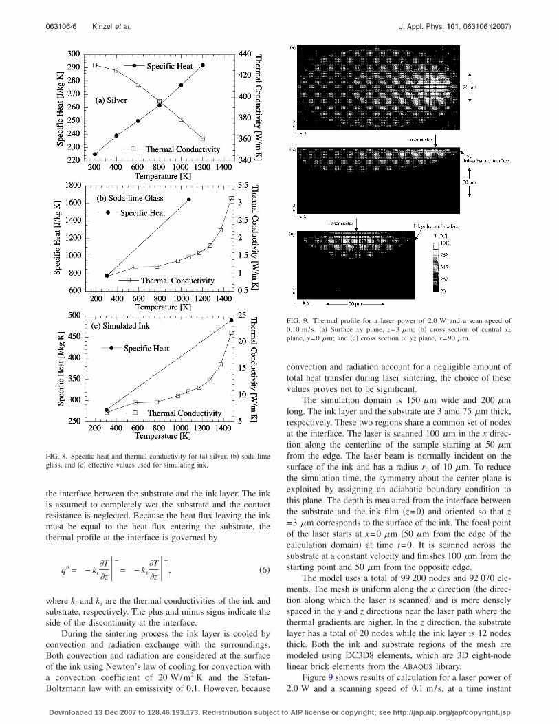
Figure 9 shows results of calculation for a laser power of2.0 W and a scanning speed of 0.1 m/s, at a time instant
FIG. 8. Specific heat and thermal conductivity for �a� silver, �b� soda-limeglass, and �c� effective values used for simulating ink.
FIG. 9. Thermal profile for a laser power of 2.0 W and a scan speed of0.10 m/s. �a� Surface xy plane, z=3 �m; �b� cross section of central xzplane, y=0 �m; and �c� cross section of yz plane, x=90 �m.
063106-6 Kinzel et al. J. Appl. Phys. 101, 063106 �2007�
Downloaded 13 Dec 2007 to 128.46.193.173. Redistribution subject to AIP license or copyright; see http://jap.aip.org/jap/copyright.jsp
when the center of the laser is located 90 �m from the be-ginning of scan. The figure shows the region of the heatedarea including the discontinuity of temperature gradient atthe interface between the substrate and the ink layer. It isworth pointing out that the depth of thermal penetration intothe substrate is confined within several micrometers from theinterface.
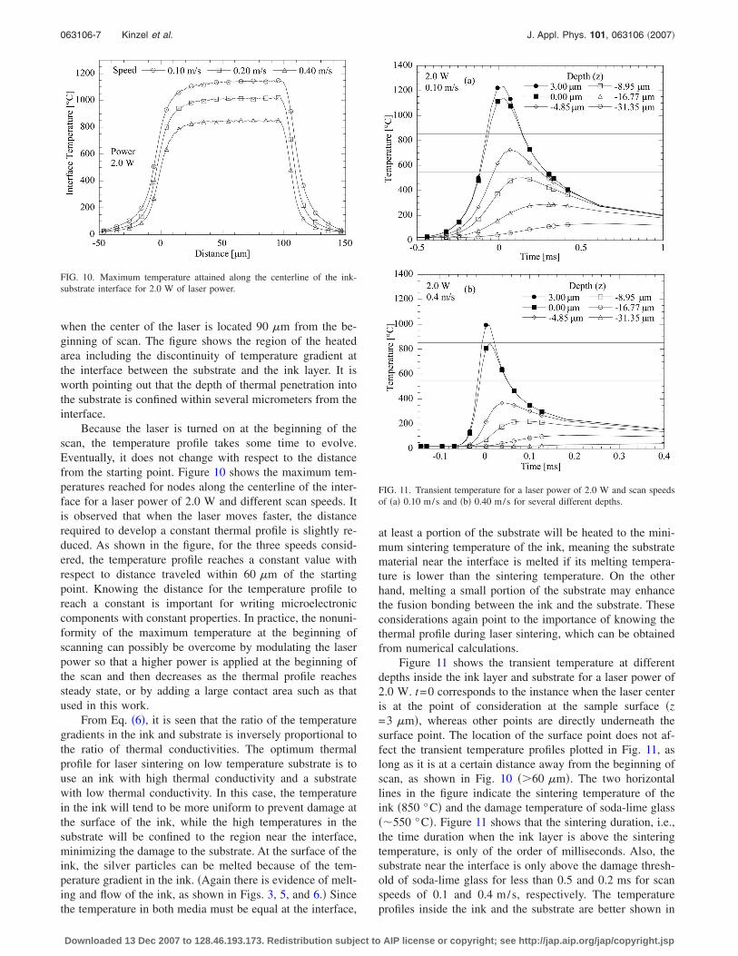
Because the laser is turned on at the beginning of thescan, the temperature profile takes some time to evolve.Eventually, it does not change with respect to the distancefrom the starting point. Figure 10 shows the maximum tem-peratures reached for nodes along the centerline of the inter-face for a laser power of 2.0 W and different scan speeds. Itis observed that when the laser moves faster, the distancerequired to develop a constant thermal profile is slightly re-duced. As shown in the figure, for the three speeds consid-ered, the temperature profile reaches a constant value withrespect to distance traveled within 60 �m of the startingpoint. Knowing the distance for the temperature profile toreach a constant is important for writing microelectroniccomponents with constant properties. In practice, the nonuni-formity of the maximum temperature at the beginning ofscanning can possibly be overcome by modulating the laserpower so that a higher power is applied at the beginning ofthe scan and then decreases as the thermal profile reachessteady state, or by adding a large contact area such as thatused in this work.
From Eq. �6�, it is seen that the ratio of the temperaturegradients in the ink and substrate is inversely proportional tothe ratio of thermal conductivities. The optimum thermalprofile for laser sintering on low temperature substrate is touse an ink with high thermal conductivity and a substratewith low thermal conductivity. In this case, the temperaturein the ink will tend to be more uniform to prevent damage atthe surface of the ink, while the high temperatures in thesubstrate will be confined to the region near the interface,minimizing the damage to the substrate. At the surface of theink, the silver particles can be melted because of the tem-perature gradient in the ink. �Again there is evidence of melt-ing and flow of the ink, as shown in Figs. 3, 5, and 6.� Sincethe temperature in both media must be equal at the interface,
at least a portion of the substrate will be heated to the mini-mum sintering temperature of the ink, meaning the substratematerial near the interface is melted if its melting tempera-ture is lower than the sintering temperature. On the otherhand, melting a small portion of the substrate may enhancethe fusion bonding between the ink and the substrate. Theseconsiderations again point to the importance of knowing thethermal profile during laser sintering, which can be obtainedfrom numerical calculations.
Figure 11 shows the transient temperature at differentdepths inside the ink layer and substrate for a laser power of2.0 W. t=0 corresponds to the instance when the laser centeris at the point of consideration at the sample surface �z=3 �m�, whereas other points are directly underneath thesurface point. The location of the surface point does not af-fect the transient temperature profiles plotted in Fig. 11, aslong as it is at a certain distance away from the beginning ofscan, as shown in Fig. 10 ��60 �m�. The two horizontallines in the figure indicate the sintering temperature of theink �850 °C� and the damage temperature of soda-lime glass��550 °C�. Figure 11 shows that the sintering duration, i.e.,the time duration when the ink layer is above the sinteringtemperature, is only of the order of milliseconds. Also, thesubstrate near the interface is only above the damage thresh-old of soda-lime glass for less than 0.5 and 0.2 ms for scanspeeds of 0.1 and 0.4 m/s, respectively. The temperatureprofiles inside the ink and the substrate are better shown in
FIG. 10. Maximum temperature attained along the centerline of the ink-substrate interface for 2.0 W of laser power.
FIG. 11. Transient temperature for a laser power of 2.0 W and scan speedsof �a� 0.10 m/s and �b� 0.40 m/s for several different depths.
063106-7 Kinzel et al. J. Appl. Phys. 101, 063106 �2007�
Downloaded 13 Dec 2007 to 128.46.193.173. Redistribution subject to AIP license or copyright; see http://jap.aip.org/jap/copyright.jsp
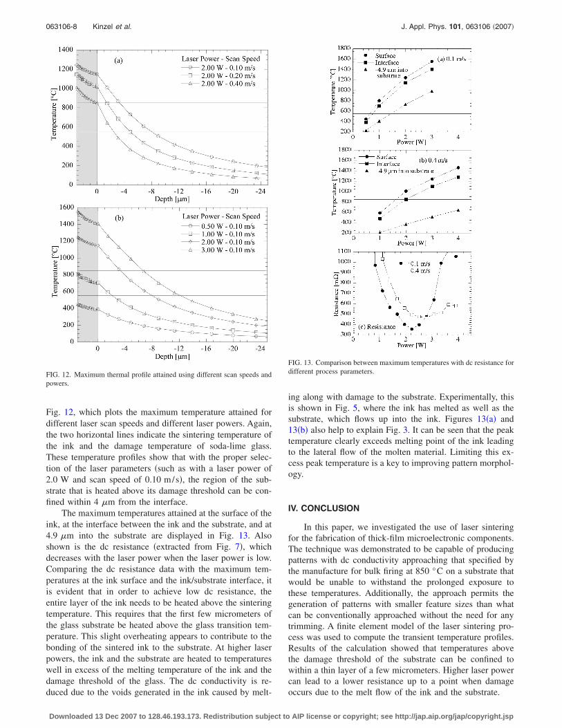
Fig. 12, which plots the maximum temperature attained fordifferent laser scan speeds and different laser powers. Again,the two horizontal lines indicate the sintering temperature ofthe ink and the damage temperature of soda-lime glass.These temperature profiles show that with the proper selec-tion of the laser parameters �such as with a laser power of2.0 W and scan speed of 0.10 m/s�, the region of the sub-strate that is heated above its damage threshold can be con-fined within 4 �m from the interface.
The maximum temperatures attained at the surface of theink, at the interface between the ink and the substrate, and at4.9 �m into the substrate are displayed in Fig. 13. Alsoshown is the dc resistance �extracted from Fig. 7�, whichdecreases with the laser power when the laser power is low.Comparing the dc resistance data with the maximum tem-peratures at the ink surface and the ink/substrate interface, itis evident that in order to achieve low dc resistance, theentire layer of the ink needs to be heated above the sinteringtemperature. This requires that the first few micrometers ofthe glass substrate be heated above the glass transition tem-perature. This slight overheating appears to contribute to thebonding of the sintered ink to the substrate. At higher laserpowers, the ink and the substrate are heated to temperatureswell in excess of the melting temperature of the ink and thedamage threshold of the glass. The dc conductivity is re-duced due to the voids generated in the ink caused by melt-
ing along with damage to the substrate. Experimentally, thisis shown in Fig. 5, where the ink has melted as well as thesubstrate, which flows up into the ink. Figures 13�a� and13�b� also help to explain Fig. 3. It can be seen that the peaktemperature clearly exceeds melting point of the ink leadingto the lateral flow of the molten material. Limiting this ex-cess peak temperature is a key to improving pattern morphol-ogy.
IV. CONCLUSION
In this paper, we investigated the use of laser sinteringfor the fabrication of thick-film microelectronic components.The technique was demonstrated to be capable of producingpatterns with dc conductivity approaching that specified bythe manufacture for bulk firing at 850 °C on a substrate thatwould be unable to withstand the prolonged exposure tothese temperatures. Additionally, the approach permits thegeneration of patterns with smaller feature sizes than whatcan be conventionally approached without the need for anytrimming. A finite element model of the laser sintering pro-cess was used to compute the transient temperature profiles.Results of the calculation showed that temperatures abovethe damage threshold of the substrate can be confined towithin a thin layer of a few micrometers. Higher laser powercan lead to a lower resistance up to a point when damageoccurs due to the melt flow of the ink and the substrate.
FIG. 12. Maximum thermal profile attained using different scan speeds andpowers.
FIG. 13. Comparison between maximum temperatures with dc resistance fordifferent process parameters.
063106-8 Kinzel et al. J. Appl. Phys. 101, 063106 �2007�
Downloaded 13 Dec 2007 to 128.46.193.173. Redistribution subject to AIP license or copyright; see http://jap.aip.org/jap/copyright.jsp
ACKNOWLEDGMENTS
The authors wish to gratefully acknowledge the State ofIndiana’s 21st Century Research and Development Fund forsupporting this work. They would also like to thank CarlBerlin at Delphi Delco Electronics Systems for providing thematerials and constructive feedback as well as Dr. RichardX. Zhang for assistance with setting up the FEM simulations.One of the authors �E.C.K.� also thanks the Lozar Fellowshipof the School of Mechanical Engineering, Purdue University.
1J. J. Licari and L. R. Enlow, Hybrid Microcircuit Technology Handbook,2nd ed. �Noyes, Westwood, NJ, 1998�.
2N. R. Bieri, J. Chung, D. Poulikakos, and C. P. Grigoropoulos, Appl. Phys.A: Mater. Sci. Process. 80, 1485 �2005�.
3A. Piqué and D. B. Chrisey, Direct-Write Technologies for Rapid Proto-typing Applications: Sensors, Electronics, and Integrated Power Sources�Academic, San Diego, 2002�.
4V. Marinov, J. Microelectronics Packaging 1, 261 �2004�.
5H. Sigmarsson, E. Kinzel, W. Chappell, and X. Xu, Antennas and Propa-gation Society International Symposium, Washington, DC, 3–8 July 2005�IEEE, New York,2005�, Vol. 1A, pp. 280–283.
6E. Kinzel, H. Sigmarsson, X. Xu, and W. Chappell, 35th European Micro-wave Conference Proceedings, European Microwave Association, Paris,France, 4–6 October 2005 �IEEE, New York,2005�, Vol. 1, pp. 289–292.
7H. Sigmarsson, E. Kinzel, W. Chappell, and X. Xu, Microwave Sympo-sium Digest, IEEE MTT-S International, San Fransisco, CA, 12–17 June2006 �IEEE, New York,2006�, pp. 1788–1791.
8D. A. Willis and X. Xu, J. Heat Transfer 122, 763 �2000�.9T. R. Shiu, C. P. Grigoropoulos, D. G. Cahill, and R. Greif, J. Appl. Phys.86, 1311 �1999�.
10J. C. Maxwell, Electricity and Magnetism, 3rd ed. �Clarendon, Oxford,1904�, Pt. II, p. 440.
11F. P. Incropera and D. P. Dewitt, Fundamentals of Heat and Mass Transfer�Wiley, New York, 2002�.
12H. Kiyohashi, N. Hayakawa, S. Aratani, and H. Masuda, High Temp. -High Press. 34, 167 �2002�.
13Y. S. Touloukian, Thermophysical of Properties of Matter: Specific Heatof Nonmetallic Solids �Plenum, New York, 1972�, Vol. 5, pp. 1240–1242.
063106-9 Kinzel et al. J. Appl. Phys. 101, 063106 �2007�
Downloaded 13 Dec 2007 to 128.46.193.173. Redistribution subject to AIP license or copyright; see http://jap.aip.org/jap/copyright.jsp