Embed Size (px)
Citation preview

Large surface relaxation in the organic semiconductor
tetracene
Hazuki Morisaki1, Takashi Koretsune2, Chisa Hotta3, Jun Takeya4,
Tsuyoshi Kimura1, and Yusuke Wakabayashi1∗
1Division of Materials Physics, Graduate School of Engineering Science,
Osaka University, Toyonaka 560-8531, Japan
2RIKEN Center for Emergent Matter Science (CEMS), Wako, Saitama 351-0198, Japan
3Graduate School of Arts and Science, University of Tokyo, Meguro 153-8902, Japan
4Graduate School of Frontier Sciences, Univ. Tokyo, Kashiwa 277-8561, Japan
September 24, 2014
Abstract
Organic crystals are likely to have a large degree of structural relaxation near their surfaces
because of the weak inter-molecular interactions. The design of organic field-effect transis-
tors requires a detailed knowledge of the surface relaxation as the carriers usually transfer
within the first few molecular layers at the semiconductor surfaces, and their transport
properties reflect the structural changes through the transfer integral. Here, we report
the direct observation of the surface relaxation of an organic semiconductor, a tetracene
single crystal, by means of X-ray crystal truncation rod scattering measurements. A sig-
nificant degree of surface relaxation is observed, taking place only in the first monolayer
at the semiconductor surface. First principles calculations show that the resultant transfer
integrals are completely different between the bulk and surface of the semiconductor.
∗e-mail: [email protected]
1

Crystals have different structures at their surfaces, known as surface relaxation or
surface reconstruction. While they are central issues of surface science, they have less
impact on the transport properties of inorganic semiconductors.1 The surface conductivity
originates from the surface-state bands as well as from the bending of the bulk-band, which
occurs at the space-charge layer; For surfaces with few adatoms, the former contribution is
minor. In the case of organic semiconductors, a significant degree of surface relaxation is
likely to occur because of the weak inter-molecular elastic interactions. The resultant self-
organized, self-repairing surface layer is expected to have very different electric properties
to its bulk counterpart because the inter-molecular electron transfer is sensitive to the
molecular arrangement. If the range of the surface relaxation extends as thick as the
space charge layer, the surface transport properties will be completely different from that
expected in the bulk. Such surface conductivity is even more important in electronic
devices.
The application of organic semiconductors in electronic devices has rapidly grown in
recent years. Organic electroluminescent displays and organic solar cells are already com-
mercially available. Interfacial charge transfer makes the interface of two insulating organic
crystals conductive.2 In spintronics, organic semiconductors are regarded as attractive ma-
terials for use in spin valve devices because of their ability to maintain the spin polarization
of the carriers.3 Most of the functionalities of organic semiconductors are provided by the
electron transfer at their interfaces. In fact, the conduction in organic field-effect tran-
sistors (OFETs) is confined to the first few molecular layers (∼ 1 nm) at the surfaces4
when the applied gate electric field is as large as 1 MV cm−1, which is a normal value for
OFETs. Therefore, knowledge of the surface structure of organic semiconductors is essen-
tial to understand the microscopic mechanism of the transport properties and to design
ideal organic devices with characteristics different from conventional inorganic devices.
The attempt to clarify the surface structure is first made in the organic ultrathinfilms
on SiO2 substrates,5—7 which imitate organic thin-film-transistors. However, the best per-
formance of organic semiconductors is always found in single crystals. To take advantage
of the single crystals, an inkjet printing technique of single crystal films of organic semicon-
ductors was recently developed.8 Therefore, the surface of single crystals is of importance.
Structural information pertaining to the crystal surface is useful to better understand bulk
2

properties because the mobility, the standard measure of the performance of an organic
semiconductor, is evaluated by fabricating OFETs,9—11 which is actually the surface mo-
bility.4 Also, the transport properties in polycrystalline samples are largely affected by
scattering at the grain boundaries, which certainly is related to the detail of the interfaces;
the knowledge of the surfaces is in fact important as a first step. Recent progress in surface
X-ray scattering techniques and analysis methods made it possible to study the details
of the surface structure of complicated structured materials. The first observation of the
surface structure of organic semiconductor was made on the rubrene single crystal12 using
a combination of X-ray crystal truncation rod (CTR) scattering, which is one of the surface
X-ray scattering techniques, and holographic analysis on it.13
In this study, we perform CTR scattering measurements on tetracene single crystals.
The result shows a significant degree of surface relaxation for the first time in the crystalline
organic semiconductors, in sharp contrast with rubrene, which hardly shows relaxation.
The first principles calculation indeed optimizes such kind of relaxation, and shows that
the relaxation results in a large modification of the surface band parameters compared
to the bulk. The resultant bandwidth and mobility are both suppressed in the surface
structure.
Results
Surface structures of rubrene and tetracene single crystals
According to the kinematical theory of X-ray diffraction, the scattering amplitude is given
by the Fourier transform of the electron density. The surface is identified as the onset of
the zero electron density. Thus, the Fourier transform of the step function is generally
observed in scattering from a sample with a flat surface, which is called CTR scattering.
The CTR scattering intensity is therefore sensitive to the surface structure and is used to
study the structure of the surface.14,15
First, we demonstrate the surface electron density analysis by using rubrene (Fig. 1(f))
single crystal placed on a Si substrate. Figure 2 (a) shows the CTR scattering profile
along the (00L)-line. The black circles indicate the experimental results, which all fall on
the calculated CTR profile for the ideal surface model. Here, the ideal surface model was
3

defined as a surface with no relaxation, reconstruction or roughness.
The phase of the scattering amplitude was obtained by a holographic analysis technique
called coherent Bragg rod analysis (COBRA),13 which we already confirmed to be efficient
in the previous study.12 The CTR amplitude calculated from the ideal surface was used
as the reference wave of the hologram to analyse the relaxed surface. Figure 2 (b) shows
the electron density profile obtained from the CTR profile in panel (a). The density was
averaged over the area of the unit-cell in the c-plane. The observed electron density profile
is identical to the profile of the ideal surface model. Therefore, the freshly prepared rubrene
crystal exhibits no surface relaxation. The small amount of surface relaxation reported in
ref. 12 was caused by degradation of the sample, which occurred during the storage in air.
In contrast, we find a large degree of surface relaxation in the tetracene crystals
(Fig. 1(a-c)). Figure 2 (c) shows the (00L)-CTR profile of a tetracene crystal on a Si
substrate. The profile was reproduced over three successive measurements, showing that
the radiation damage to the sample was negligible. Different pieces of the crystal showed
similar intensity profiles, demonstrating that the surface structure of the tetracene crystal
in air was stable and reproducible. The same measurements were carried out on a crystal
attached to a glass pin, which gave the same CTR profile. This result suggests that the
substrate-side of the tetracene surface was either very rough or had the same structure as
the air-side of the tetracene surface.16 The red curve in Fig. 2 (c) shows the profile calcu-
lated for an ideal surface, which does not reproduce the experimental results. To develop a
surface model that reproduces the experimentally observed CTR profile, a grid search was
carried out by translationally shifting the molecules in the first layer, rotating them with
respect to the a- and b-axes, varying the atomic displacement parameter (B) and taking
account of the adsorbates. The solid blue curve in Fig. 2 (c) shows the best fit profile. A
schematic of the corresponding real space structure is presented in panel (e).
Using this structural model as the initial model, electron density analysis was performed
using the COBRA method with this CTR profile. Figure 2(d) shows the electron density
profile (the robustness of the resultant profile is examined in the supplementary note 1
and supplementary Fig. 1). Here, z = 0 was chosen as the nominal surface. The electron
density in the z < −3 A region, which corresponds to outside the sample, is much smallerthan that in the crystal. The z > 0 region is divided into molecular layers. From the
4

integrated electron density, each layer at z ≥ 12.15 A contains 240 electrons per unit cell,the net electron number expected in the bulk crystal. The first molecular layer ranged
from 0 ≤ z ≤ 12.15 A and has 237 electrons per unit cell, meaning that there was almostno molecular vacancies in the surface layer. The comparison of the first and the third
layers indicates that the surface layer expands by 5.2% along the c-direction. This amount
of expansion can be explained by rotating the molecules by 15◦ about the a-axis. Excess
electrons are observed at −3 A< z < 0 A, which is attributed to either adsorbates with
18 electrons per unit cell or 37 electrons per nm2. While the present X-ray data does
not provide us with the chemical species of the adsorbed matter at the surface, one could
anticipate them as being small enough not to deteriorate the basic structure of the surface,
and is likely to be either water, nitrogen or oxygen molecules. Indeed, the atomic force
microscopy measurements in ref. 17 report that the surface of a tetracene crystal has the
same in-plane periodicity with the bulk lattice parameters.
Our experimental observations pose a question of to what extent the surface relaxation
influences the electronic transport properties. Regarding the microscopic charge transport
in the accumulation layer in OFETs, the amplitudes of the quantum tunnelling between
the highest occupied molecular orbitals (HOMOs), namely the transfer integrals, play a
primary role.18 Therefore, the molecular arrangement is crucial for all of the proposed
models ranging from the incoherent hopping to the coherent band-like transport models,
which are still under debate. Experimentally, band dispersion measurements by means of
photoelectron spectroscopy have been performed on thin films to prevent the charge-up
problem,19—21 and the reports on single crystal samples are limited.22,23 The theoretical
studies on the transport properties reported thus far have been based on bulk single crys-
tals.24—29 Moreover, none of the studies have taken the surface structure relaxation into
account. In our tetracene crystals, the surface relaxation significantly modified the transfer
integrals, as demonstrated in the following section.
First principles calculations
On the basis of the above experimental analysis on tetracene, we performed the first prin-
ciples electronic structure calculations with the generalized-gradient approximation in the
framework of the density functional theory (DFT). The resultant energy bands are shown
5

in Fig. 3, where a significant difference between the bulk and surface bands can be seen.
The transfer integrals along the paths shown in Fig. 1(b) were calculated using the DFT
band structure of the bulk and the surface. The values, together with the effective masses
of the holes, are outlined in Table 1. While the changes in the effective masses are minor,
the transfer integrals ta and tb show large differences. The tight binding energy bands
are analytically obtained using the parameters in Table 1 (see Supplementary note 2 and
Supplementary Fig. 2).
The information on the in-plane structure obtained in the experiments was rather am-
biguous compared with that along the direction perpendicular to the surface (see Fig. 2(d)).
This is because of the experimental difficulty caused by the twinned triclinic crystals having
common c*-axis, which hampers the CTR measurements other than (00L)-line. To com-
pensate for this, we carried out structural optimization of the “surface” layer by putting it
on top of a single layer with fixed “bulk structure” obtained in the experiments. We tried
several choices of functionals of DFT, finding that although they showed a large amount
of relaxation, the way of relaxing depends quite much on the functionals. The optimized
structure of soft organic crystals governed by the van der Waals interactions is often known
to deviate quantitatively from the experimental structure. Furthermore, the choice of only
a single bulk layer attached to a surface might not be enough to reproduce a real crystal.
For these reasons, it is not proper to determine the most suitable relaxed crystal structure
solely from the calculations that compare the energies of several candidate structures. Still,
we find a reasonable solution that has the similar surface-layer-width with the results of
the CTR measurements, which is shown in Fig. 2(f). As we see, the angle between the
surface and the long molecular axis in the surface molecular layer is closer to 90◦ than that
in the bulk. This situation is similar to the thin film phase pentacene6,30 as presented in
Figs. 1 (d) and (e).
Discussion
As discussed earlier, the effect of surface relaxation is directly reflected in the large dif-
ference of the energy dispersions and in the values of the transfer integrals(see Table 1).
The HOMO bandwidth of the bulk and the surface are 0.39 and 0.26 eV, respectively, as
6

presented in Fig. 3. This already indicates that the tetracene surface is less conductive
than bulk. To further examine the effect of relaxation on the transport properties, we
give a qualitative estimation on the mobility based on these transfer integrals, where we
followed the theoretical treatment based on one of the incoherent hopping models.31 This
treatment gives straightforward results, comparable to the experiments and is adopted to
the fragment analysis in the DFT-based quantum chemistry calculations. The calculated
bulk and the surface mobilities were 1.2 cm2V−1s−1 and 0.3 cm2V−1s−1 at 300 K (see sup-
plementary note 3 for details; we used the value of the reorganization energy given in ref. 32
in this calculation). The surface mobility at 300 K was very close to the maximum value
of the mobility of tetracene (0.4 cm2V−1s−1), which was measured in a high-gate-voltage
FET.11 We should, however, mention that this estimate is at most the semi-quantitative
one. There are many other models that are used to determine the mobilities of organic
crystals, but discussing the quality of each of the theoretical models is beyond the scope
of this study. Still, we would like to argue that the surface relaxation in tetracene makes
the surface less conductive by a factor of 1.5 to 3.
Now, the two organic semiconductors, rubrene and tetracene, will be compared. The
rubrene molecule is obtained by decorating the edges of tetracene molecule with four phenyl
substitutions (see Fig. 1(f)). The distribution of the HOMOs on these two molecules are
almost the same.18 However, rubrene barely shows a surface relaxation, in sharp contrast
to tetracene. This should be because the decorated part of the rubrene molecule works as
a structural steric barrier, which does not allow the molecules to tilt freely with respect
to the layer. As a result, even though the shapes of HOMOs are the same, the energy
band structures and the transport properties represented by the mobility completely differ
between the two. This indicates that the choice of the molecular shape should be the key
to efficiently controlling the degree of surface relaxation in organic crystals.
Finally, a recent report on the photoelectron spectroscopy on rubrene and tetracene
single crystals will be discussed.23 Reference 23 reported a clear band structure of rubrene
in agreement with the theoretical prediction,18 whereas, the signal of the HOMO band of
the tetracene showed severe broadening, which did not reproduce a reasonable band disper-
sion. While they attribute the broadening to the effect of phonon or to the surface disorder,
we consider that the latter effect should be small as we find in our X-ray measurement.
7

Our present analysis could instead give another more reasonable scenario; the relaxation
taking place only at the single surface layer produces a set of surface energy bands which
significantly differ from the bulk, and the overlap of signals between the surface and the
bulk energy bands smears out the details of each of them. This scenario also accounts for
the clear dispersion in rubrene, as it has little surface relaxation.
In conclusion, CTR scattering measurements were performed on tetracene single crys-
tals and a significant degree of surface relaxation was observed for the first time in organic
semiconductors. The details on the molecular structure at the surfaces were clarified by
analysing the experimental electron density profile obtained using COBRA, as well as with
the first principles calculations. The relaxation was limited to the first molecular layer in
the semiconductor, while the relaxed layer was already as thick as the charge accumula-
tion layer in the OFETs, which contributed to the carrier transport. This study clearly
demonstrates that the surface relaxation of long-shaped molecules could lead to a qualita-
tive change in its transport properties at the surface. Appropriate design of the molecular
structure is the key to controlling the degree of the surface relaxation, which will provide
a path to fabricate functional self-organizing surfaces for use in molecular devices.
Methods
Sample
The tetracene crystals were grown by physical vapor transport using a two-zone tube
furnace under a continuous stream of Ar gas at a rate of 80 cm3 per minute. The diameter
of the tube was 20 mm. The upper-stream high-temperature zone was maintained at 220 ◦C
to sublime the tetracene raw materials (sublime grade), purchased from Aldrich Co. The
downstream zone was heated to 160 ◦C to form crystals, typically in 1—2 days. The rubrene
crystals were also made in a similar manner.
The typical size of the crystals used for the CTR measurements was 2 mm × 1 mm
in area and several micrometres thick. X-ray oscillation photography confirmed that the
structures of the tetracene crystals were the same as the one reported in ref. 33. The lattice
parameters used were a = 6.075 A, b = 7.93 A, c = 13.46 A, α = 66.6◦, β = 101◦, and
γ = 94◦, as shown in Figs. 1 (a) and (b). The surface topographies of the crystals were
8
measured with an atomic force microscope (Nanocute, SII nanotechnology) in the dynamic
force mode (Fig. 1 (c)).
Surface X-ray scattering experiments and electron density analysis
The CTR scattering experiments were carried out using BL-4C and 3A at the Photon Fac-
tory, KEK, Japan. The beamlines are equipped with standard four-circle diffractometers
that had a silicon drift detector. X-rays with an energy of 12 keV were used. The spot size
was 0.5 mm × 0.5 mm. All of the experiments were performed in air at room temperature
and the data were collected using transverse scans to subtract the background. Radiation
damage to the samples was monitored by repeating the measurements several times.
The crystals were placed on Si (001) substrates or attached to glass pins for the CTR
measurements. The measurements were performed within a week from the crystal growth.
In contrast, in our previous study,12 the rubrene crystal was kept in air for several month.
Coherent Bragg rod analysis was performed using a homemade code with an interpo-
lated experimental dataset. Because electron density analysis requires a wide q-range of
intensity data, the experimental data with calculated intensities below ζ = 1.9 and some
regions with almost no intensity as well as the regions close to the Bragg reflections were
substituted. It was confirmed that the main feature of the electron density was not sensitive
to the model used for the substitution, indicating the validity of the analysis method.
DFT calculations
The ultrasoft pseudopotentials and the plane-wave basis set with cutoff energies of 30 Ry
for wave functions and 200 Ry for charge densities were used. For the surface band struc-
tures, supercell calculations were performed for experimental single-layer structure. The
ground state charge densities were computed using 4 × 4 × 2 k-point samplings for the
bulk electronic structures, and 4 × 4 × 1 k-points for the surface electronic structures,
respectively. To obtain the transfer integrals, we construct a maximally localized Wannier
orbital for each tetracene.
For the geometry optimization, the system consisting of three molecular layers was
considered, with one bulk layer sandwiched between two open surface layers. By assuming
9

the in-plane periodicity of each layer, the structure was optimized with fixing the bulk layer
atoms. Such setup was expected to reproduce the surface relaxation at the two end layers,
since the experimental results support that the bulk crystal structure was maintained
already at the second layer from the surface.
References
[1] Hasegawa, S., Tong, X., Takeda, S., Sato, N. & Nagao, T. Structures and electronic
transport on silicon surfaces, Prog. Surf. Sci. 60, 89-257 (1999).
[2] Alves, H., Molinari,A. S., Xie, H. & Morpurgo, A. F. Metallic conduction at organic
charge-transfer interfaces. Nat. Mater. 7, 574-580 (2008).
[3] Dediu, V. A., Hueso, L.E., Bergenti, I. & Taliani,C. Spin routes in organic semicon-
ductors. Nat. Mater. 8, 707-716 (2009).
[4] Takeya, J. et al. Very high-mobility organic single-crystal transistors with in-crystal
conduction channels. Appl. Phys. Lett. 90, 102120 (2007).
[5] Kowarik, S., Gerlach, A., Sellner, S., Schreiber, F., Cavalcanti, L. & Konovalov, O.
Real-Time Observation of Structural and Orientational Transitions during Growth of
Organic Thin Films, Phys. Rev. Lett. 96 125504 (2006).
[6] Schiefer, S., Huth, M., Dobrinevski, A. & Nickel, B. Determination of the Crystal
Structure of Substrate-Induced Pentacene Polymorphs in Fiber Structured Thin Films.
J. Am. Chem. Soc. 129, 10316 (2007).
[7] Mannsfeld, S.C.B., Virkar, A., Reese, C., Toney, F. & Bao, Z. Precise Structure of
Pentacene Monolayers on Amorphous Silicon Oxide and Relation to Charge Transport.
Adv. Mat. 21 2294-2298 (2009).
[8] Minemawari, H., Yamada, T., Matsui, H., Tsutsumi, J., Haas, S., Chiba, R., Kumai,
R. & Hasegawa, T. Inkjet printing of single-crystal films. Nature 475 364-367 (2011).
10
[9] Reese, C., Chung, W.-J., Ling, M.-M., Roberts, M. & Bao, Z. High-performance
microscale single-crystal transistors by lithography on an elastomer dielectric. Appl.
Phys. Lett. 89, 202108 (2006)
[10] Butko, V. Y., Chi, X. & Ramirez, A.P., Free-standing tetracene single crystal field
effect transistor. Solid State Commun. 128, 431-434 (2003).
[11] de Boer, R.W.I., Klapwijk, T.M. & Morpurgo, A.F. Field-effect transistors on
tetracene single crystals, Appl. Phys. Lett. 83 4345-4347 (2003).
[12] Wakabayashi, Y., Takeya, J. & Kimura, T. Sub-A resolution electron density analysis
of the surface of organic rubrene crystals, Phys. Rev. Lett. 104 066103 (2010).
[13] Yacoby, Y. et al. Direct determination of epitaxial interface structure in Gd2O3 pas-
sivation of GaAs, Nat. Mater. 1 99-101, (2002).
[14] Robinson, I.K. Crystal truncation rods and surface roughness, Phys. Rev. B 33 3830-
3836 (1986).
[15] P. R. Willmott et al., Structural Basis for the Conducting Interface between LaAlO3
and SrTiO3. Phys. Rev. Lett. 99, 155502 (2007).
[16] Wakabayashi, Y., Takeya, J. & Kimura, T. Interface structure of the rubrene crystal
field effect transistor, J. Appl. Phys., 110 102206 (2011).
[17] Overney, R.M., Howald, L., Frommer, J., Meyer, E. & Guntherodt, H.-J. Molecular
surface structure of tetracene mapped by the atomic force microscope, J. Chem. Phys.
94 8441-8443 (1991).
[18] da Silva Filho, D.A., Kim, E.-G. & Bredas, J.-L. Transport Properties in the Rubrene
Crystal: Electronic Coupling and Vibrational Reorganization Energy, Adv. Matter.
17, 1072 (2005).
[19] Koch, N. et al. Evidence for Temperature-Dependent Electron Band Dispersion in
Pentacene, Phys. Rev. Lett. 96, 156803 (2006).
[20] Kakuta, H. et al. Electronic Structures of the Highest Occupied Molecular Orbital
Bands of a Pentacene Ultrathin Film, Phys. Rev. Lett. 98, 247601 (2007).
11

[21] Ohtomo, M., Suzuki, T., Shimada, T. & Hasegawa, T. Band dispersion of quasi-single
crystal thin film phase pentacene monolayer studied by angle-resolved photoelectron
spectroscopy, Appl. Phys. Lett. 95 123308 (2009).
[22] Machida, S., Nakayama, Y., Duhm, S., Xin, Q., Funakoshi, A., Ogawa, N., Kera,
S., Ueno, N. & Ishii, H. Highest-Occupied-Molecular-Orbital Band Dispersion of
Rubrene Single Crystals as Observed by Angle-Resolved Ultraviolet Photoelectron
Spectroscopy, Phys. Rev. Lett. 104, 156401 (2010).
[23] Vollmer, A. et al. Two dimensional band structure mapping of organic single crystals
using the new generation electron energy analyzer ARTOF, J.Electron Spectroscopy
and Related Phenomena 185 55-60 (2012) .
[24] de Wijs, G.A., Mattheus, C.C., de Groot, R.A. & Palstra, T.T.M. Anisotropy of the
mobility of pentacene from frustration, Synth. Met. 139 109-114 (2003).
[25] Hummer, K. & Ambrosch-Draxl, C. Electronic properties of oligoacenes from first
principles, Phys. Rev. B 72, 205205 (2005).
[26] Ambrosch-Draxl, C., Nabok, D., Puschnig, P. & Meisenbichler, C. The role of poly-
morphism in organic thin films: oligoacenes investigated from first principles, New J.
Phys. 11 125010 (2009).
[27] Ortmann, F., Bechstedt, F. & Hannewald, K. Charge transport in organic crys-
tals:Theory and modelling, Phys. Status Solidi B 248, 511-525 (2011).
[28] Li, Y., Coropceanu, V. & Bredas, J.-L. Thermal Narrowing of the Electronic Band-
widths in Organic Molecular Semiconductors: Impact of the Crystal Thermal Expan-
sion, J. Phys. Chem. Lett. 3, 3325-3329 (2012).
[29] Yanagisawa, S., Morikawa, Y. & Schindlmayr, A. HOMO band dispersion of crystalline
rubrene: Effects of self-energy corrections within the GW approximation, Phys. Rev.
B 88, 115438 (2013).
[30] Campbell, R.B., Robertson, J.M. & Trotter, J. The Crystal and Molecular Structure
of Pentacene, Acta Cryst. 14, 705-711 (1961).
12

[31] Deng, W.-Q. & Goddard III, W.A. Predictions of Hole Mobilities in Oligoacene Or-
ganic Semiconductors from Quantum Mechanical Calculations, J. Phys. Chem. B 108,
8614-8621 (2004).
[32] Rossi, M. & Sohlberg, K. Predictions of Hole Mobility in Molecular Organic Crystals:
Incorporating Thermal Effects, J. Phys. Chem. C, 113 6821-6831 (2009).
[33] Robertson, J.M., Sinclair, V.C. & Trotter, J. The Crystal and Molecular Structure of
Tetracene, Acta Cryst. 14, 697-704 (1961).
Acknowledgements
The authors thank Prof. K. Ueno, Prof. T. Takahashi and Dr T. Shirasawa for their
valuable discussions. The single crystals were grown with the help of Dr Y. Okada. This
work was supported by Grants-In-Aid for Scientific Research (JSPS KAKENHI, Grant Nos
23684026, 26287080, 26105008), the Toray Science Foundation and the TEPCO Memorial
Foundation.
Author contributions
H. M. and Y. W. performed the X-ray diffraction measurements and analysis. J. T. grew the
single crystal samples. T. K. performed the first principles calculations. The project was
designed by Y. W. and the manuscript was written by Y. W. and C. H. with contributions
from all authors.
Additional information
Competing financial interests: The authors declare no competing financial interests.
13

Figure 1: Crystal structures of tetracene and pentacene. The tetracene crystal structure
seen from (a) the a-axis and (b) the c-axis. The lattice parameters are a = 6.075 A,
b = 7.93 A, c = 13.46 A, α = 66.6◦, β = 101◦, and γ = 94◦. The in-plane transfer
paths are indicated with arrows. (c) AFM image of a tetracene crystal. (d) the bulk-
polymorph structure30 (lattice parameters a = 6.14 A, b = 7.93 A, c = 16.03 A, α = 67.4◦,
β = 101.9◦, and γ = 94.2◦) and (e) The thin-film-polymorph structure6 (lattice parameters
a = 5.958 A, b = 7.596 A, c = 15.61 A, α = 81.25◦, β = 86.56◦, and γ = 89.8◦). (f) The
molecular structures of rubrene, tetracene and pentacene.
14
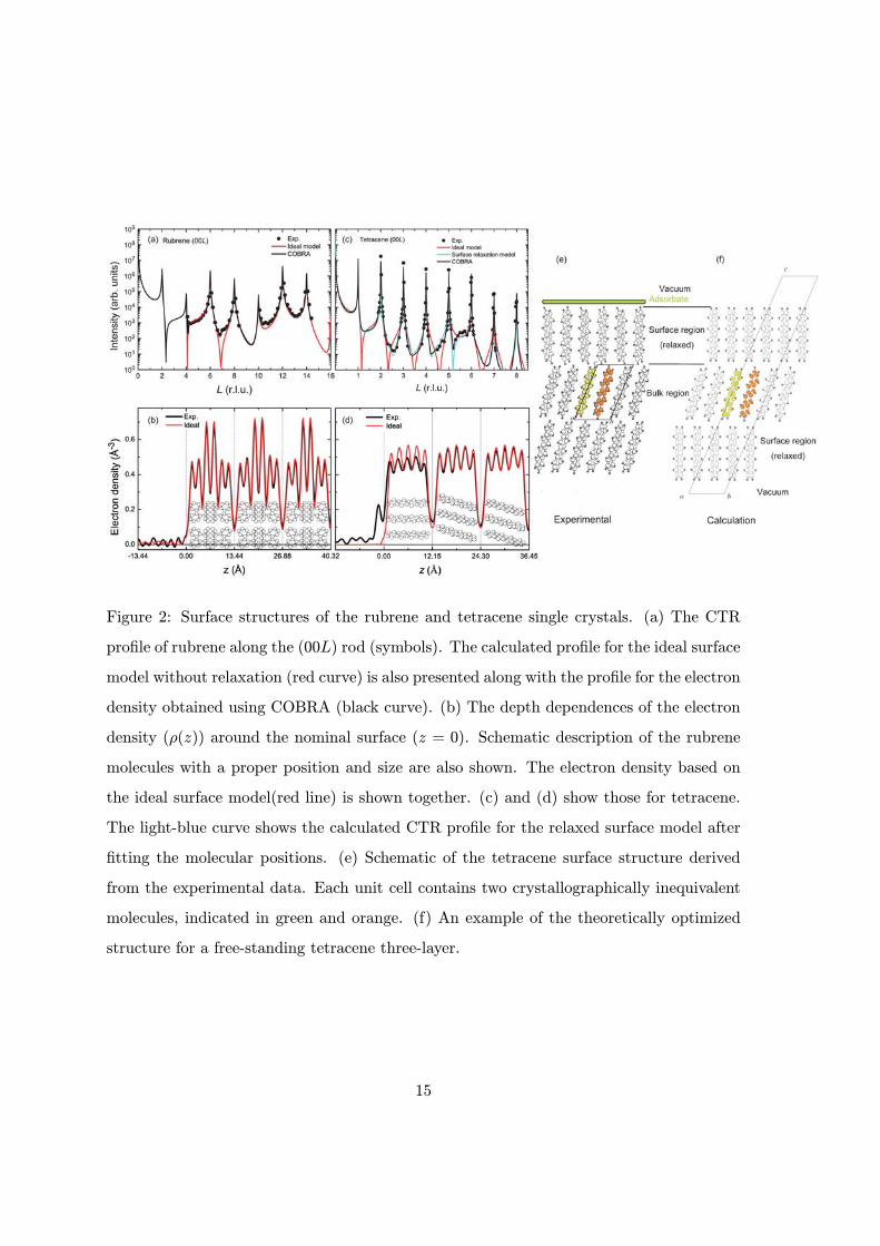
Figure 2: Surface structures of the rubrene and tetracene single crystals. (a) The CTR
profile of rubrene along the (00L) rod (symbols). The calculated profile for the ideal surface
model without relaxation (red curve) is also presented along with the profile for the electron
density obtained using COBRA (black curve). (b) The depth dependences of the electron
density (ρ(z)) around the nominal surface (z = 0). Schematic description of the rubrene
molecules with a proper position and size are also shown. The electron density based on
the ideal surface model(red line) is shown together. (c) and (d) show those for tetracene.
The light-blue curve shows the calculated CTR profile for the relaxed surface model after
fitting the molecular positions. (e) Schematic of the tetracene surface structure derived
from the experimental data. Each unit cell contains two crystallographically inequivalent
molecules, indicated in green and orange. (f) An example of the theoretically optimized
structure for a free-standing tetracene three-layer.
15

Figure 3: In-plane band diagram derived from experimentally obtained bulk and surface
structures. The left panel shows the band dispersions along the (0,0)-(1/2,1/2) (Γ-L) line
and the right panel shows those along the (1/2,0)-(0,0)-(0,1/2) (X-Γ-Y )line. The origin of
the energy is chosen to the valence band maximum.
Table 1: Transfer integrals of tetracene bulk and surface. The energy differences of the
on-site energies for the two crystallographically independent molecules (e1 − e2) are alsolisted. The effective masses of the holes are also listed using the unit of the electron mass
me.
bulk surface
t1(meV) 16 16
t2(meV) -14 -14
ta(meV) -19 -37
tb(meV) 65 -24
e1 − e2(meV) -97 -37
mx (me) 6.6 6.9
my (me) 2.6 3.8
16
-36.45 -24.30 -12.15 0.00 12.15 24.30 36.450.0
0.1
0.2
0.3
0.4
0.5
0.6
0.7
Initial value COBRA
Ele
ctro
n de
nsity
(Å-3
)
Depth (Å)
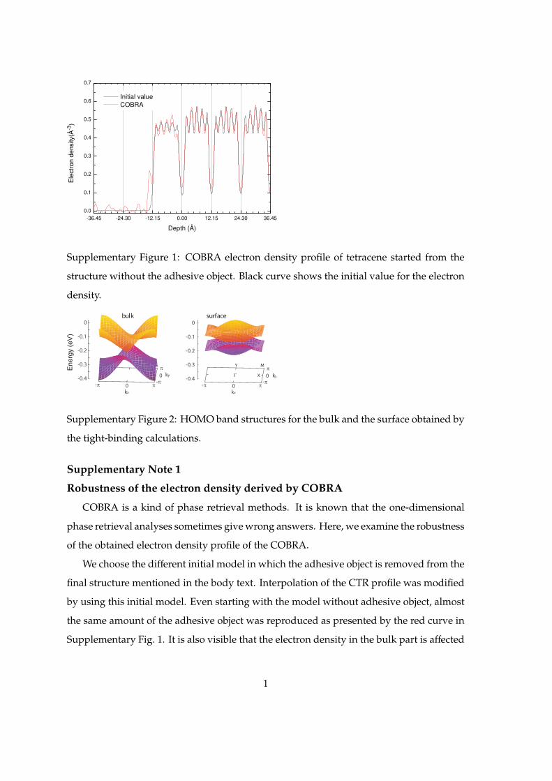
Supplementary Figure 1: COBRA electron density profile of tetracene started from the
structure without the adhesive object. Black curve shows the initial value for the electron
density.
- 0
0
-
ky
kx
- 0
0
-
ky
kx
-0.4
-0.3
-0.2
-0.1
0
bulk surface
-0.4
-0.3
-0.2
-0.1
0
X
MY
Energ
y (
eV
)
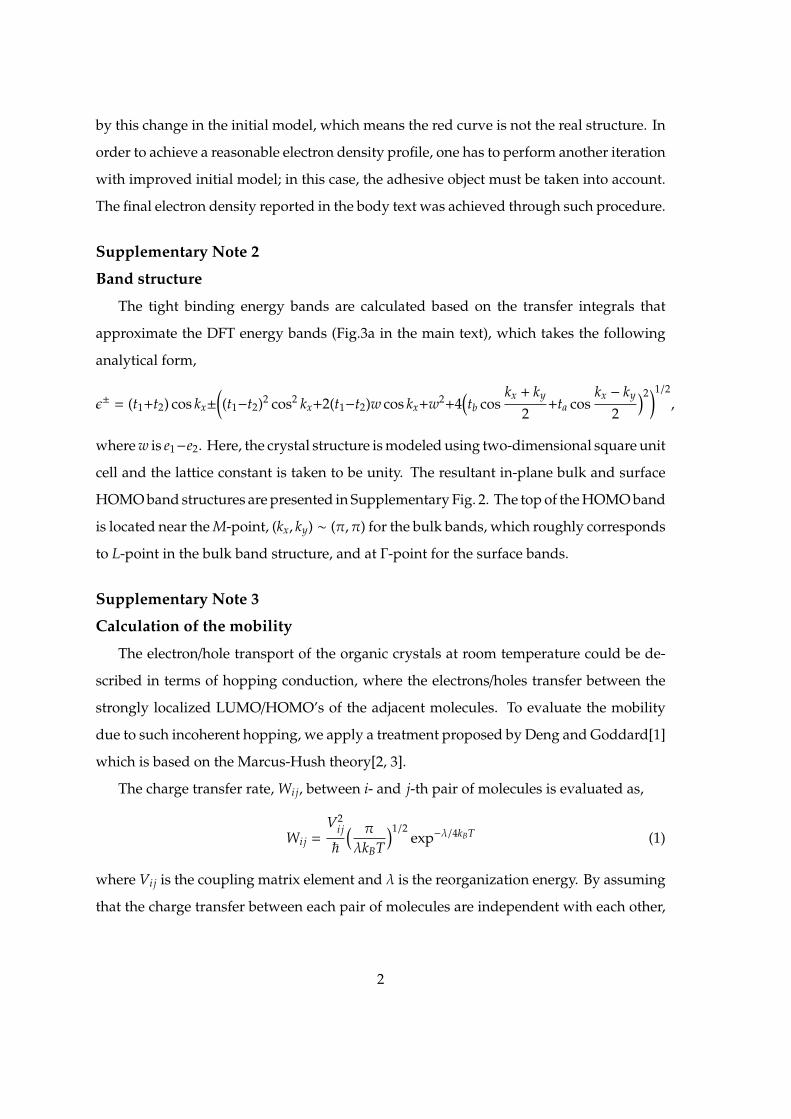
Supplementary Figure 2: HOMO band structures for the bulk and the surface obtained by
the tight-binding calculations.
Supplementary Note 1
Robustness of the electron density derived by COBRA
COBRA is a kind of phase retrieval methods. It is known that the one-dimensional
phase retrieval analyses sometimes give wrong answers. Here, we examine the robustness
of the obtained electron density profile of the COBRA.
We choose the different initial model in which the adhesive object is removed from the
final structure mentioned in the body text. Interpolation of the CTR profile was modified
by using this initial model. Even starting with the model without adhesive object, almost
the same amount of the adhesive object was reproduced as presented by the red curve in
Supplementary Fig. 1. It is also visible that the electron density in the bulk part is affected
1
by this change in the initial model, which means the red curve is not the real structure. In
order to achieve a reasonable electron density profile, one has to perform another iteration
with improved initial model; in this case, the adhesive object must be taken into account.
The final electron density reported in the body text was achieved through such procedure.
Supplementary Note 2
Band structure
The tight binding energy bands are calculated based on the transfer integrals that
approximate the DFT energy bands (Fig.3a in the main text), which takes the following
analytical form,
ϵ± = (t1+t2) cos kx±((t1−t2)2 cos2 kx+2(t1−t2)w cos kx+w2+4
(tb cos
kx + ky
2+ta cos
kx − ky
2
)2)1/2,
where w is e1−e2. Here, the crystal structure is modeled using two-dimensional square unit
cell and the lattice constant is taken to be unity. The resultant in-plane bulk and surface
HOMO band structures are presented in Supplementary Fig. 2. The top of the HOMO band
is located near the M-point, (kx, ky) ∼ (π, π) for the bulk bands, which roughly corresponds
to L-point in the bulk band structure, and at Γ-point for the surface bands.
Supplementary Note 3
Calculation of the mobility
The electron/hole transport of the organic crystals at room temperature could be de-
scribed in terms of hopping conduction, where the electrons/holes transfer between the
strongly localized LUMO/HOMO’s of the adjacent molecules. To evaluate the mobility
due to such incoherent hopping, we apply a treatment proposed by Deng and Goddard[1]
which is based on the Marcus-Hush theory[2, 3].
The charge transfer rate, Wi j, between i- and j-th pair of molecules is evaluated as,
Wi j =V2
i j
~
( πλkBT
)1/2exp−λ/4kBT (1)
where Vi j is the coupling matrix element and λ is the reorganization energy. By assuming
that the charge transfer between each pair of molecules are independent with each other,
2

one could obtain the diffusion constant in the following form,
D = ⟨ 12d
∑j
r2i jWi jPi j⟩i=1,2, Pi j =
Wi j∑Wi j
(2)
where for ⟨· · · ⟩i=1,2 we take the mean value over the two independent molecules in a unit
cell, and j runs over the six neighboring molecules of i-th molecule. ri j is the distance
between adjacent molecules and d = 3 is the system dimension.
The Einstein’s relation gives the mobility in the following form,
µ =e
kBTD. (3)
In our first principles calculation, we constructed the maximally-localized Wannier
orbital on each HOMO, and evaluated the transfer integrals, ti j, between them and the
difference of on-site energies of the two independent molecules, e1 − e2, as listed in Table 1
in the main text. Based on these data, the coupling matrix element is obtained as, Vi j =√t2i j + (ei − e j)2/4.
The distances between molecules corresponding to the connections, t1, t2, ta and tb
are 6.07, 6.07, 5.16, and 4.82Å, respectively. We take the renormalization energy of the
tetracene single molecule as λ = 0.117eV from Ref. [4].
At room temperature T =300K, we find µ = 1.29 cm2V−1s−1 (bulk) and 0.33 cm2V−1s−1
(surface).
Supplementary References
[1] Deng, W.-Q. & Goddard III, W.A. Predictions of Hole Mobilities in Oligoacene Organic
Semiconductors from Quantum Mechanical Calculations, J. Phys. Chem. B 108, 8614-
8621 (2004).
[2] Marcus, R.A. Chemical and electrochemical electron-transfer theory, Annu. Rev. Phys.
Chem. 15, 155-196 (1964).
[3] Marcus, R. A. On the Theory of Oxidation-Reduction Reactions Involving Electron
Transfer, I. J. Chem. Phys. 24, 966-978 (1955).
3

[4] Rossi, M. & Sohlberg, K. Predictions of Hole Mobility in Molecular Organic Crystals:
Incorporating Thermal Effects, J. Phys. Chem. C, 113 6821-6831 (2009).
4

![Transition from spin-orbit to hyperfine interaction ... · traditional, direct excitons (DXs) in semiconductor quantum wells [25]. Because hole spin relaxation is usually much faster](https://img.pdfslide.us/doc/110x75/5e1f39f844e5b7747314401b/transition-from-spin-orbit-to-hyperine-interaction-traditional-direct-excitons.jpg)