Embed Size (px)
Citation preview
JLMN-Journal of Laser Micro/Nanoengineering Vol. 13, No. 3, 2018
254
Large Scale Ultrafast Laser Micro Texturing with Multi-Beams
S. Bruening1, M. Jarczynski2,, K. Du3 and A. Gillner4
1 Schepers GmbH & Co. KG, Karl-Benz Str. 7, 48691 Vreden, Germany E-mail: [email protected]
2 Limo GmbH, Germany 3 Edgewave GmbH, Germany
4 Fraunhofer ILT, Germany
Today ultrashort pulse lasers (USP lasers) are already widely used to realize highly precise micro-structures directly in nearly any material. Despite of today’s availability of high power ultrashort pulse lasers (up to several hundred watts), it is still a challenge to structure large surface areas, as required on embossing rollers, within an acceptable processing time for industrial production. A newly developed high compact ps-laser with repetition rates of up to 8MHz and an average power of up to 500W was distributed into 8 parallel beamlets by a diffractive optical element (DOE). Each of the single beams in the array is controlled by an acousto optical modulator (AOM). The beam array was focused on a cylinder surface with spot sizes of 10µm. Based on this initial set up, a further improved optical systems with 16 single beams has been designed to increase ablation speed and productivity. The beams have a distance of 20µm (8 beamlets) respective 80µm (16 beamlets) from spot to spot. Integrated in an ultra-high precision cylinder engraving system, the spots were synchronized with a precision of <1µm. Different functional surface geometries have been realized on an embossing roller as a master, which is used for the replication of the structures in roll-to-roll (R2R) processes. With this setup, functional structures as e.g. reduction in friction, improved soft touch or light guiding elements can be generated on large surfaces within short pro-cessing times.
Keywords: usp-laser, diffractive optical element DOE, acuosto optical modulator AOM, multi spot, parallel micro processing, 3D micro structures, surface functionalization, metal sheet embossing, roll-to-roll micro embossing, nano imprint lithography (NIL), intaglio print
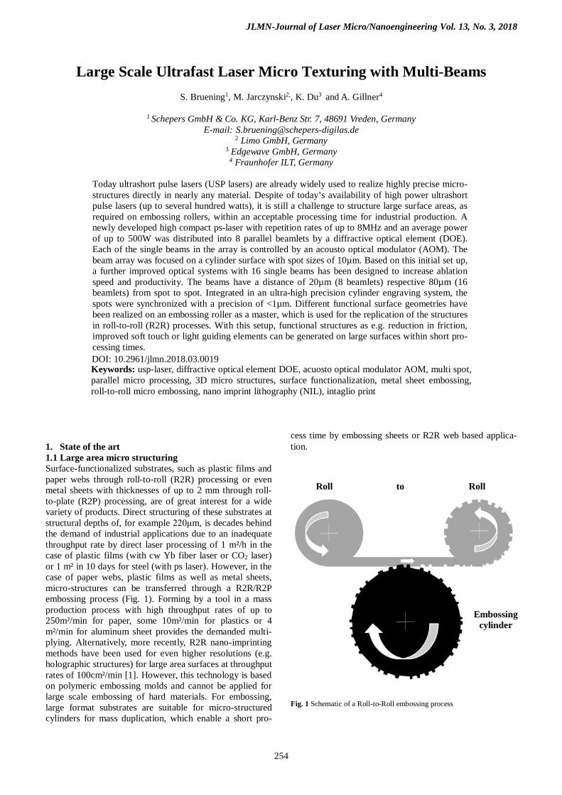
1. State of the art 1.1 Large area micro structuring Surface-functionalized substrates, such as plastic films and paper webs through roll-to-roll (R2R) processing or even metal sheets with thicknesses of up to 2 mm through roll-to-plate (R2P) processing, are of great interest for a wide variety of products. Direct structuring of these substrates at structural depths of, for example 220μm, is decades behind the demand of industrial applications due to an inadequate throughput rate by direct laser processing of 1 m²/h in the case of plastic films (with cw Yb fiber laser or CO2 laser) or 1 m² in 10 days for steel (with ps laser). However, in the case of paper webs, plastic films as well as metal sheets, micro-structures can be transferred through a R2R/R2P embossing process (Fig. 1). Forming by a tool in a mass production process with high throughput rates of up to 250m²/min for paper, some 10m²/min for plastics or 4 m²/min for aluminum sheet provides the demanded multi-plying. Alternatively, more recently, R2R nano-imprinting methods have been used for even higher resolutions (e.g. holographic structures) for large area surfaces at throughput rates of 100cm²/min [1]. However, this technology is based on polymeric embossing molds and cannot be applied for large scale embossing of hard materials. For embossing, large format substrates are suitable for micro-structured cylinders for mass duplication, which enable a short pro-
cess time by embossing sheets or R2R web based applica-tion.
Fig. 1 Schematic of a Roll-to-Roll embossing process
Roll to Roll
Embossing cylinder
DOI: 10.2961/jlmn.2018.03.0019
JLMN-Journal of Laser Micro/Nanoengineering Vol. 13, No. 3, 2018
255
1.2 Tooling embossing cylinders The outstanding quality of ultrashort pulse lasers offers a material-independent, almost melt-free removal due to the extremely short pulses and the high pulse energy. A system based disadvantage, however, is the very low productivity compared to ns laser pulses. For achieving a high level of productivity, on the one hand high pulse repetition rates are necessary, but on the other hand a scaling of the number of spots is inevitable. One application that can systematically achieve high scanning speeds is the engraving of emboss-ing and printing cylinders. As, in this case, the workpiece is rotationally symmetric (Fig. 2), a very high uniform pe-ripheral speed can be achieved. A freely modulated laser spot allows three-dimensional structures to be transferred to the cylinder surface. With resolutions of 5080 dpi (pixel size 5μm) and 44 W laser power, surface speeds of 10 m/s in 4 mm³/min for steel are possible in a cylinder engraving system. These speeds can be increased by four beam sources to about 16 mm³/min which still means a process time of 10 days for an area of 1 m² with a depth of 220μm in steel [2].
Fig. 2 Multi-Laser / Multi-Beam Approach
In the BMBF project MULTISURF, further process accel-eration was pursued by increasing the number of laser spots. The aim of the project was to distribute high-performance USP laser sources from a few 100 W to up to 100 individually modulated spots, and thus shortening the process times (Fig. 3). This paper presents the application of cylindrical micro-structuring, the generation and modu-lation of many individual parallel-ablating spots on the cylinder and some representative applications.
Fig. 3 Single Laser / Multi-Beam Approach
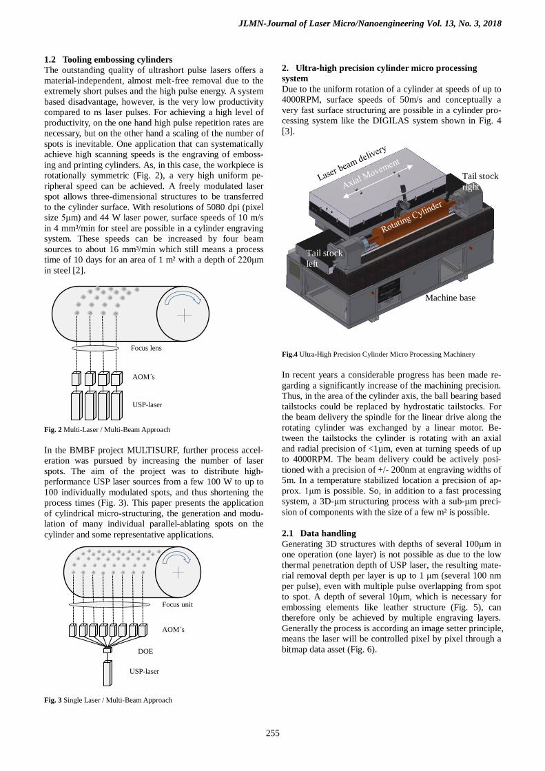
2. Ultra-high precision cylinder micro processing system Due to the uniform rotation of a cylinder at speeds of up to 4000RPM, surface speeds of 50m/s and conceptually a very fast surface structuring are possible in a cylinder pro-cessing system like the DIGILAS system shown in Fig. 4 [3].
Fig.4 Ultra-High Precision Cylinder Micro Processing Machinery
In recent years a considerable progress has been made re-garding a significantly increase of the machining precision. Thus, in the area of the cylinder axis, the ball bearing based tailstocks could be replaced by hydrostatic tailstocks. For the beam delivery the spindle for the linear drive along the rotating cylinder was exchanged by a linear motor. Be-tween the tailstocks the cylinder is rotating with an axial and radial precision of <1µm, even at turning speeds of up to 4000RPM. The beam delivery could be actively posi-tioned with a precision of +/- 200nm at engraving widths of 5m. In a temperature stabilized location a precision of ap-prox. 1μm is possible. So, in addition to a fast processing system, a 3D-μm structuring process with a sub-μm preci-sion of components with the size of a few m² is possible.
2.1 Data handling Generating 3D structures with depths of several 100μm in one operation (one layer) is not possible as due to the low thermal penetration depth of USP laser, the resulting mate-rial removal depth per layer is up to 1 μm (several 100 nm per pulse), even with multiple pulse overlapping from spot to spot. A depth of several 10μm, which is necessary for embossing elements like leather structure (Fig. 5), can therefore only be achieved by multiple engraving layers. Generally the process is according an image setter principle, means the laser will be controlled pixel by pixel through a bitmap data asset (Fig. 6).
Focus lens
USP-laser
AOM´s
Focus unit
USP-laser
AOM´s
DOE
Tail stock right
Machine base
Tail stock left
JLMN-Journal of Laser Micro/Nanoengineering Vol. 13, No. 3, 2018
256
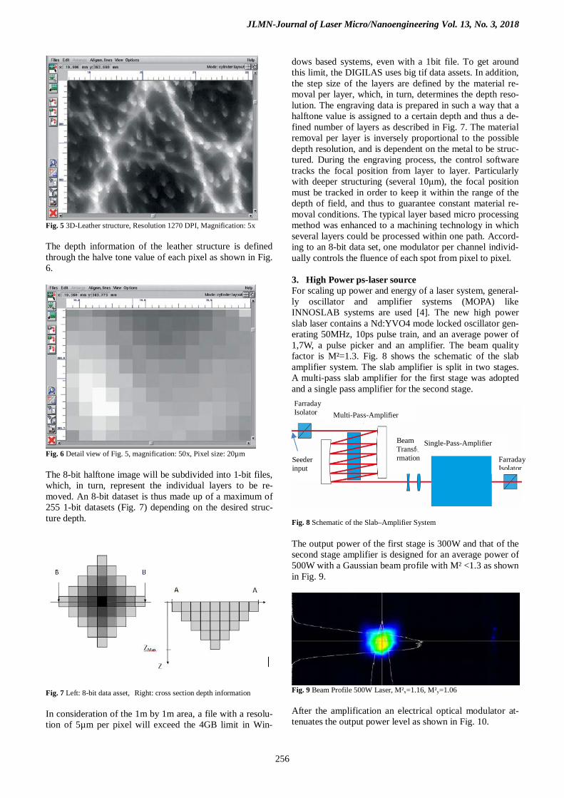
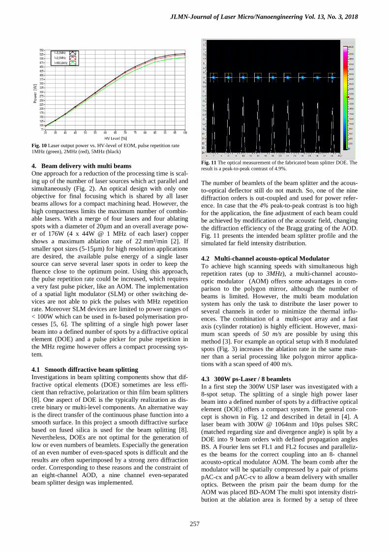
Fig. 5 3D-Leather structure, Resolution 1270 DPI, Magnification: 5x The depth information of the leather structure is defined through the halve tone value of each pixel as shown in Fig. 6.
Fig. 6 Detail view of Fig. 5, magnification: 50x, Pixel size: 20µm The 8-bit halftone image will be subdivided into 1-bit files, which, in turn, represent the individual layers to be re-moved. An 8-bit dataset is thus made up of a maximum of 255 1-bit datasets (Fig. 7) depending on the desired struc-ture depth.
Fig. 7 Left: 8-bit data asset, Right: cross section depth information In consideration of the 1m by 1m area, a file with a resolu-tion of 5µm per pixel will exceed the 4GB limit in Win-
dows based systems, even with a 1bit file. To get around this limit, the DIGILAS uses big tif data assets. In addition, the step size of the layers are defined by the material re-moval per layer, which, in turn, determines the depth reso-lution. The engraving data is prepared in such a way that a halftone value is assigned to a certain depth and thus a de-fined number of layers as described in Fig. 7. The material removal per layer is inversely proportional to the possible depth resolution, and is dependent on the metal to be struc-tured. During the engraving process, the control software tracks the focal position from layer to layer. Particularly with deeper structuring (several 10μm), the focal position must be tracked in order to keep it within the range of the depth of field, and thus to guarantee constant material re-moval conditions. The typical layer based micro processing method was enhanced to a machining technology in which several layers could be processed within one path. Accord-ing to an 8-bit data set, one modulator per channel individ-ually controls the fluence of each spot from pixel to pixel. 3. High Power ps-laser source For scaling up power and energy of a laser system, general-ly oscillator and amplifier systems (MOPA) like INNOSLAB systems are used [4]. The new high power slab laser contains a Nd:YVO4 mode locked oscillator gen-erating 50MHz, 10ps pulse train, and an average power of 1,7W, a pulse picker and an amplifier. The beam quality factor is M²=1.3. Fig. 8 shows the schematic of the slab amplifier system. The slab amplifier is split in two stages. A multi-pass slab amplifier for the first stage was adopted and a single pass amplifier for the second stage.
Fig. 8 Schematic of the Slab–Amplifier System
The output power of the first stage is 300W and that of the second stage amplifier is designed for an average power of 500W with a Gaussian beam profile with M² <1.3 as shown in Fig. 9.
Fig. 9 Beam Profile 500W Laser, M²x=1.16, M²y=1.06 After the amplification an electrical optical modulator at-tenuates the output power level as shown in Fig. 10.
Multi-Pass-Amplifier
Seeder input
Beam Transformation
Single-Pass-Amplifier
Farraday Isolator
Farraday Isolator
JLMN-Journal of Laser Micro/Nanoengineering Vol. 13, No. 3, 2018
257
Fig. 10 Laser output power vs. HV-level of EOM, pulse repetition rate 1MHz (green), 2MHz (red), 5MHz (black)
4. Beam delivery with multi beams One approach for a reduction of the processing time is scal-ing up of the number of laser sources which act parallel and simultaneously (Fig. 2). An optical design with only one objective for final focusing which is shared by all laser beams allows for a compact machining head. However, the high compactness limits the maximum number of combin-able lasers. With a merge of four lasers and four ablating spots with a diameter of 20µm and an overall average pow-er of 176W (4 x 44W @ 1 MHz of each laser) copper shows a maximum ablation rate of 22 mm³/min [2]. If smaller spot sizes (5-15µm) for high resolution applications are desired, the available pulse energy of a single laser source can serve several laser spots in order to keep the fluence close to the optimum point. Using this approach, the pulse repetition rate could be increased, which requires a very fast pulse picker, like an AOM. The implementation of a spatial light modulator (SLM) or other switching de-vices are not able to pick the pulses with MHz repetition rate. Moreover SLM devices are limited to power ranges of < 100W which can be used in fs-based polymerisation pro-cesses [5, 6]. The splitting of a single high power laser beam into a defined number of spots by a diffractive optical element (DOE) and a pulse picker for pulse repetition in the MHz regime however offers a compact processing sys-tem.
4.1 Smooth diffractive beam splitting Investigations in beam splitting components show that dif-fractive optical elements (DOE) sometimes are less effi-cient than refractive, polarization or thin film beam splitters [8]. One aspect of DOE is the typically realization as dis-crete binary or multi-level components. An alternative way is the direct transfer of the continuous phase function into a smooth surface. In this project a smooth diffractive surface based on fused silica is used for the beam splitting [8]. Nevertheless, DOEs are not optimal for the generation of low or even numbers of beamlets. Especially the generation of an even number of even-spaced spots is difficult and the results are often superimposed by a strong zero diffraction order. Corresponding to these reasons and the constraint of an eight-channel AOD, a nine channel even-separated beam splitter design was implemented.
Fig. 11 The optical measurement of the fabricated beam splitter DOE. The result is a peak-to-peak contrast of 4.9%. The number of beamlets of the beam splitter and the acous-to-optical deflector still do not match. So, one of the nine diffraction orders is out-coupled and used for power refer-ence. In case that the 4% peak-to-peak contrast is too high for the application, the fine adjustment of each beam could be achieved by modification of the acoustic field, changing the diffraction efficiency of the Bragg grating of the AOD. Fig. 11 presents the intended beam splitter profile and the simulated far field intensity distribution.
4.2 Multi-channel acousto-optical Modulator To achieve high scanning speeds with simultaneous high repetition rates (up to 3MHz), a multi-channel acousto-optic modulator (AOM) offers some advantages in com-parison to the polygon mirror, although the number of beams is limited. However, the multi beam modulation system has only the task to distribute the laser power to several channels in order to minimize the thermal influ-ences. The combination of a multi-spot array and a fast axis (cylinder rotation) is highly efficient. However, maxi-mum scan speeds of 50 m/s are possible by using this method [3]. For example an optical setup with 8 modulated spots (Fig. 3) increases the ablation rate in the same man-ner than a serial processing like polygon mirror applica-tions with a scan speed of 400 m/s. 4.3 300W ps-Laser / 8 beamlets In a first step the 300W USP laser was investigated with a 8-spot setup. The splitting of a single high power laser beam into a defined number of spots by a diffractive optical element (DOE) offers a compact system. The general con-cept is shown in Fig. 12 and described in detail in [4]. A laser beam with 300W @ 1064nm and 10ps pulses SRC (matched regarding size and divergence angle) is split by a DOE into 9 beam orders with defined propagation angles BS. A Fourier lens set FL1 and FL2 focuses and paralleliz-es the beams for the correct coupling into an 8- channel acousto-optical modulator AOM. The beam comb after the modulator will be spatially compressed by a pair of prisms pAC-cx and pAC-cv to allow a beam delivery with smaller optics. Between the prism pair the beam dump for the AOM was placed BD-AOM The multi spot intensity distri-bution at the ablation area is formed by a setup of three
JLMN-Journal of Laser Micro/Nanoengineering Vol. 13, No. 3, 2018
258
lenses TL1, TL2, TL3 and can be rotated around the propa-gation axis by a Dove prism DP [4].
Fig. 12 Diffractive beam splitting of a 300W laser into 8 independently modulated beams, each about 29W ± 1W at focus.
The important factors of this multi beam setup are the pitch precision, the spot uniformity and the efficiency of the beam splitting by the DOE in combination with the AOM. The pitch in the target plane is 20µm ± 0.5µm and the 1/e2-spot diameter is about 8µm. The overall power non-uniformity among the maxima is below 16% (Fig. 13), and the overall efficiency is about 78% in the target plane.
Fig. 13 Beamlets in target plane
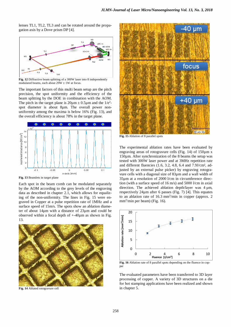
Each spot in the beam comb can be modulated separately by the AOM according to the grey levels of the engraving data as described in chapter 2.1, which allows for equaliz-ing of the non-uniformity. The lines in Fig. 15 were en-graved in Copper at a pulse repetition rate of 1MHz and a surface speed of 15m/s. The spots show an ablation diame-ter of about 14µm with a distance of 23µm and could be observed within a focal depth of +-40µm as shown in Fig. 13.
Fig. 14 Ablated rotogravure cell
Fig. 15 Ablation of 8 parallel spots The experimental ablation rates have been evaluated by engraving areas of rotogravure cells (Fig. 14) of 150µm x 150µm. After synchronization of the 8 beams the setup was tested with 300W laser power and at 3MHz repetition rate and different fluencies (1.6, 3.2, 4.8, 6.4 and 7.9J/cm², ad-justed by an external pulse picker) by engraving rotogra-vure cells with a diagonal size of 83µm and a wall width of 35µm at a resolution of 2000 l/cm in circumference direc-tion (with a surface speed of 16 m/s) and 5000 l/cm in axial direction. The achieved ablation depth/layer was 4 µm, respectively 24µm after 6 passes (Fig. 7) [4]. This equates to an ablation rate of 16.3 mm3/min in copper (approx. 2 mm3/min per beam) (Fig. 16).
Fig. 16 Ablation rate of 8 parallel spots depending on the fluence in cop-per The evaluated parameters have been transferred to 3D layer processing of copper. A variety of 3D structures on a die for hot stamping applications have been realized and shown in chapter 5.
0
5
10
15
20
0 2 4 6 8 10
Abla
tion
rate
[mm
³/m
in]
Fluence [J/cm²]
JLMN-Journal of Laser Micro/Nanoengineering Vol. 13, No. 3, 2018
259
4.4 500W ps-Laser / 16 beamlets In a further step an USP-laser with an average power of up to 500W has been used to increase the number of beamlets. Assuming that the adequate fluence for engraving copper dies is approx. 4 to 5 J/cm², it can be estimated that the developed 500W slab-based ps-laser driven at 3MHz could be implemented into a processing head that generates 16 beamlets with similar efficiency and the same spot size. Analog to the 8 beam path described in Fig. 12, a 1-to-17 smooth diffractive beam splitter BS in combination with two eight-channel acuosto optical modulators AOM1 and AOM2 arranged along the optical path concept reduces the pitch to 2mm (Fig. 17).
Fig. 17 Ray tracing simulation of the 16 spot beam delivery
The multi spot intensity distribution at the ablation area is formed by a setup of three lenses TL1, TL2, TL3 and can be modulated through the AOM´s. Due to the spatially re-stricted acoustic field per beamlet, the interim range of the AOM crystal could be used for transferring every 2nd beamlet without significant influence. A sophisticated ar-rangement of two 8-channel AOMs, as it is shown in Fig. 18, provides a sequential switching of the beamlets, accord-ing to the propagation direction. Owing to the longitudinal-ly separated switching planes in combination with only one mirror, providing the Bragg angle of the AOM, an accepta-ble small lateral shift of < 30µm of the beamlets, perpen-dicular to the beamlet comb axis, is achieved as shown in Fig. 19. This misalignment of the position can be compen-sated by a software synchronization adjustment. Thus, the associated prism array pairs for beamlet comb compression can also be neglected.
Fig. 18 Arrangement of two 8-channel AOM´s with a 2mm orthogonal Shift
Fig. 19 Ray tracing simulation of the beamlet comb in the target plane But since each beam path has to be modulated externally by a separate modulator per spot, the maximum number of this multi spot approach can serve between 16 and 24 spots. Limitation in this case is not the laser power, since ultra-short pulsed lasers are available in the several 100W region. Using a 500W laser and single spot energies of less than 10 µJ more than 50 single beams could be realized. The limit-ing factors are the size of the modulator-crystal, beam de-livery optics and focusing optics. Hence, the concept of laser beam splitting is limited, a further scaling up the multi spot arrays could overcome the limit. 5. Examples Applications of four different Roll-to-Roll transfer tech-niques will be described in the following section. Intaglio Print Old printing techniques such as Intaglio printing method (also copperplate or steel engraving) can be recreated thanks through the direct laser processing, Typical for this printing technique is, that more ink is applied than it would be needed for a good, legible fonts/characters, which means that these areas are sublime. Particulary for security appli-cations, this tactile structure is used as a security feature. The melt free direct 3D structuring of metal, the accelera-tion of the production, the elimination of several litho-graphical steps and an increased resolution compared to mechanical processing by diamond turning boosts the in-taglio print application. One example is the smallest achievable letter height. With a 10µm spot, letter heights of 150µm, 100µm and 50µm were engraved in Copper with a depth of 50µm as shown in letter guilloches (Fig. 20).
Fig. 20 In copper engraved letter Guilloches, heights 150µm, 100µm, 50µm, depth 50µm Used in an Intaglio press the letter heights could be trans-ferred to a paper substrate as shown in Fig. 21
SRC BS FL1 FL2
BD-Ch17
AOM1
AOM2
TL1 TL2 TL3
JLMN-Journal of Laser Micro/Nanoengineering Vol. 13, No. 3, 2018
260
Fig. 21 Structured plate from Fig. 19 printed on a paper substrate in R2R process Even the smallest letter height of 50µm was readable on the printed substrate. Metal sheet Embossing Aluminum sheets with thicknesses of up to 1,5mm and sizes of 1-2m² for technical and decorative applications can be rotative embossed by a hardened steel cylinder with processing speeds of 4m²/min. The transfer from the die to the aluminum sheet is realized by a deformation and mate-rial flow that allow a very faithful copy of the embossing tool (Fig. 22).
Fig. 22 Top view of an embossed aluminum sheet with 1mm thickness A structure depth of up to 120µm was transferred to the aluminum sheet (200µm are possible) as shown in Fig. 23.
Fig. 23 In aluminum transferred angled elements with depths up to 120µm
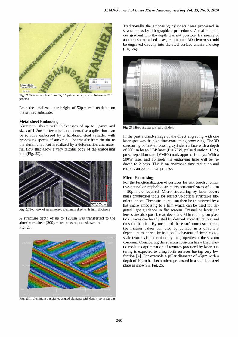
Traditionally the embossing cylinders were processed in several steps by lithographical procedures. A real continu-ous gradient into the depth was not possible. By means of an ultra-short pulsed laser, continuous 3D elements could be engraved directly into the steel surface within one step (Fig. 24).
Fig. 24 Micro structured steel cylinders In the past a disadvantage of the direct engraving with one laser spot was the high time-consuming processing. The 3D structuring of 1m² embossing cylinder surface with a depth of 200µm by an USP laser (P = 70W, pulse duration: 10 ps, pulse repetition rate 1,6MHz) took approx. 14 days. With a 500W laser and 16 spots the engraving time will be re-duced to 2 days. This is an enormous time reduction and enables an economical process. Micro Embossing For the functionalization of surfaces for soft-touch-, refrac-tive-optical or icephobic-structures structural sizes of 20µm – 50µm are required. Micro structuring by laser covers mass production tools for refractive-optical structures like micro lenses. These structures can then be transferred by a hot micro embossing to a film which can be used for tar-geted light guidance in flat screens. Fresnel or lenticular lenses are also possible as decoders. Skin rubbing on plas-tic surfaces can be adjusted by defined microstructures, and thus the haptics. By means of these soft-touch structures, the friction values can also be defined in a direction-dependent manner. The frictional behaviour of these micro-scale textures is determined by the properties of the stratum corneum. Considering the stratum corneum has a high elas-tic modulus optimization of textures produced by laser tex-turing is expected to bring forth surfaces having very low friction [4]. For example a pillar diameter of 45µm with a depth of 10µm has been micro processed in a stainless steel plate as shown in Fig. 25.
JLMN-Journal of Laser Micro/Nanoengineering Vol. 13, No. 3, 2018
261
Fig. 25 Soft touch structure: diameter: 45µm, depth: 10µm The structure was replicated and is shown in Fig. 26.
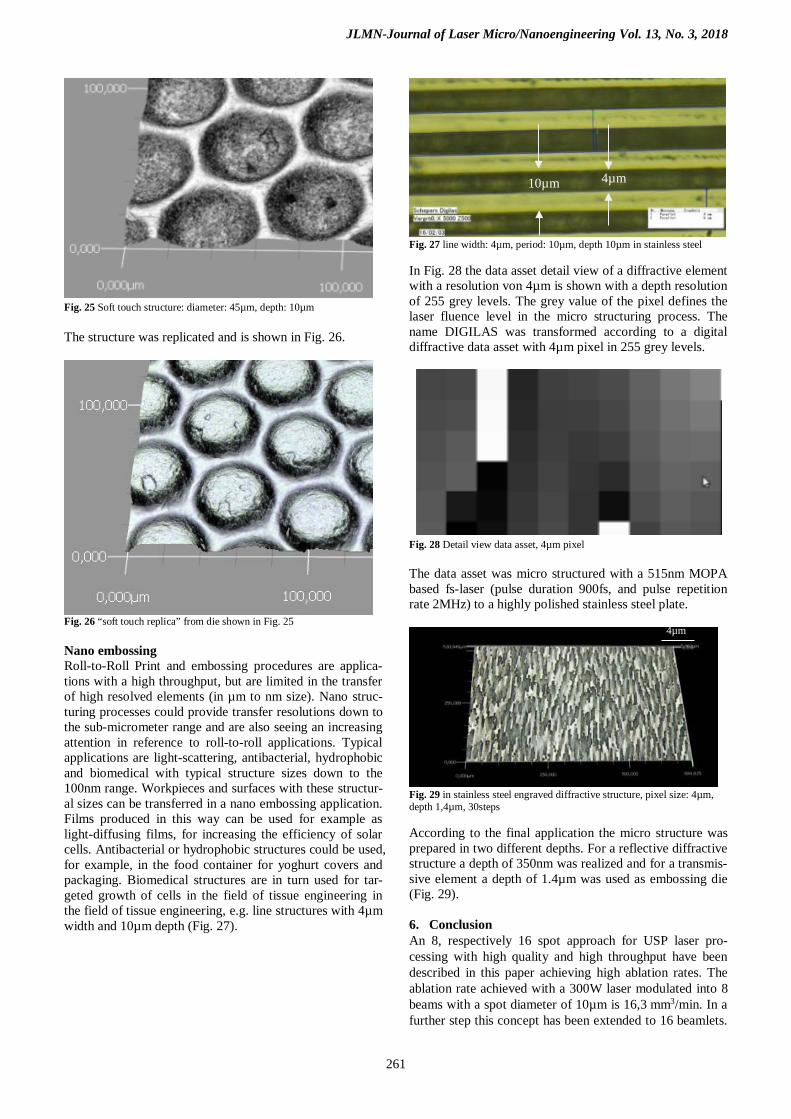
Fig. 26 “soft touch replica” from die shown in Fig. 25 Nano embossing Roll-to-Roll Print and embossing procedures are applica-tions with a high throughput, but are limited in the transfer of high resolved elements (in µm to nm size). Nano struc-turing processes could provide transfer resolutions down to the sub-micrometer range and are also seeing an increasing attention in reference to roll-to-roll applications. Typical applications are light-scattering, antibacterial, hydrophobic and biomedical with typical structure sizes down to the 100nm range. Workpieces and surfaces with these structur-al sizes can be transferred in a nano embossing application. Films produced in this way can be used for example as light-diffusing films, for increasing the efficiency of solar cells. Antibacterial or hydrophobic structures could be used, for example, in the food container for yoghurt covers and packaging. Biomedical structures are in turn used for tar-geted growth of cells in the field of tissue engineering in the field of tissue engineering, e.g. line structures with 4µm width and 10µm depth (Fig. 27).
Fig. 27 line width: 4µm, period: 10µm, depth 10µm in stainless steel In Fig. 28 the data asset detail view of a diffractive element with a resolution von 4µm is shown with a depth resolution of 255 grey levels. The grey value of the pixel defines the laser fluence level in the micro structuring process. The name DIGILAS was transformed according to a digital diffractive data asset with 4µm pixel in 255 grey levels.
4 Fig. 28 Detail view data asset, 4µm pixel The data asset was micro structured with a 515nm MOPA based fs-laser (pulse duration 900fs, and pulse repetition rate 2MHz) to a highly polished stainless steel plate.
Fig. 29 in stainless steel engraved diffractive structure, pixel size: 4µm, depth 1,4µm, 30steps According to the final application the micro structure was prepared in two different depths. For a reflective diffractive structure a depth of 350nm was realized and for a transmis-sive element a depth of 1.4µm was used as embossing die (Fig. 29). 6. Conclusion An 8, respectively 16 spot approach for USP laser pro-cessing with high quality and high throughput have been described in this paper achieving high ablation rates. The ablation rate achieved with a 300W laser modulated into 8 beams with a spot diameter of 10µm is 16,3 mm3/min. In a further step this concept has been extended to 16 beamlets.
4µm
4µm 10µm
JLMN-Journal of Laser Micro/Nanoengineering Vol. 13, No. 3, 2018
262
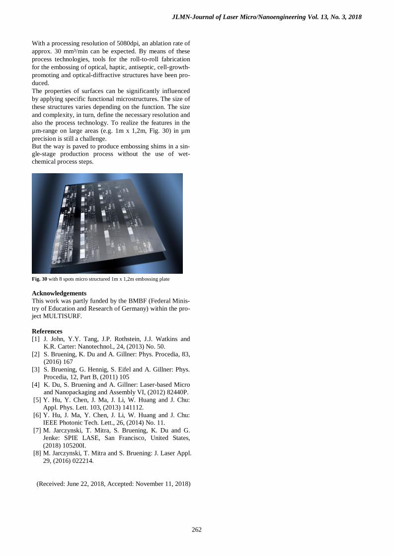
With a processing resolution of 5080dpi, an ablation rate of approx. 30 mm³/min can be expected. By means of these process technologies, tools for the roll-to-roll fabrication for the embossing of optical, haptic, antiseptic, cell-growth-promoting and optical-diffractive structures have been pro-duced. The properties of surfaces can be significantly influenced by applying specific functional microstructures. The size of these structures varies depending on the function. The size and complexity, in turn, define the necessary resolution and also the process technology. To realize the features in the µm-range on large areas (e.g. 1m x 1,2m, Fig. 30) in µm precision is still a challenge. But the way is paved to produce embossing shims in a sin-gle-stage production process without the use of wet-chemical process steps.
Fig. 30 with 8 spots micro structured 1m x 1,2m embossing plate Acknowledgements This work was partly funded by the BMBF (Federal Minis-try of Education and Research of Germany) within the pro-ject MULTISURF. References [1] J. John, Y.Y. Tang, J.P. Rothstein, J.J. Watkins and
K.R. Carter: Nanotechnol., 24, (2013) No. 50. [2] S. Bruening, K. Du and A. Gillner: Phys. Procedia, 83,
(2016) 167 [3] S. Bruening, G. Hennig, S. Eifel and A. Gillner: Phys.
Procedia, 12, Part B, (2011) 105 [4] K. Du, S. Bruening and A. Gillner: Laser-based Micro
and Nanopackaging and Assembly VI, (2012) 82440P. [5] Y. Hu, Y. Chen, J. Ma, J. Li, W. Huang and J. Chu:
Appl. Phys. Lett. 103, (2013) 141112. [6] Y. Hu, J. Ma, Y. Chen, J. Li, W. Huang and J. Chu:
IEEE Photonic Tech. Lett., 26, (2014) No. 11. [7] M. Jarczynski, T. Mitra, S. Bruening, K. Du and G.
Jenke: SPIE LASE, San Francisco, United States, (2018) 105200I.
[8] M. Jarczynski, T. Mitra and S. Bruening: J. Laser Appl. 29, (2016) 022214.
(Received: June 22, 2018, Accepted: November 11, 2018)