Embed Size (px)
Citation preview
Large scale electronic structure calculations of nanosystems using Titan machine
Lin-Wang Wang
Computational Materials Science and Nanoscience Group
Materials Sciences Division
Lawrence Berkeley National Laboratory, Berkeley, CA
US Department of Energy
BES, Office of Science
INCITE Project
NERSC, ALCF
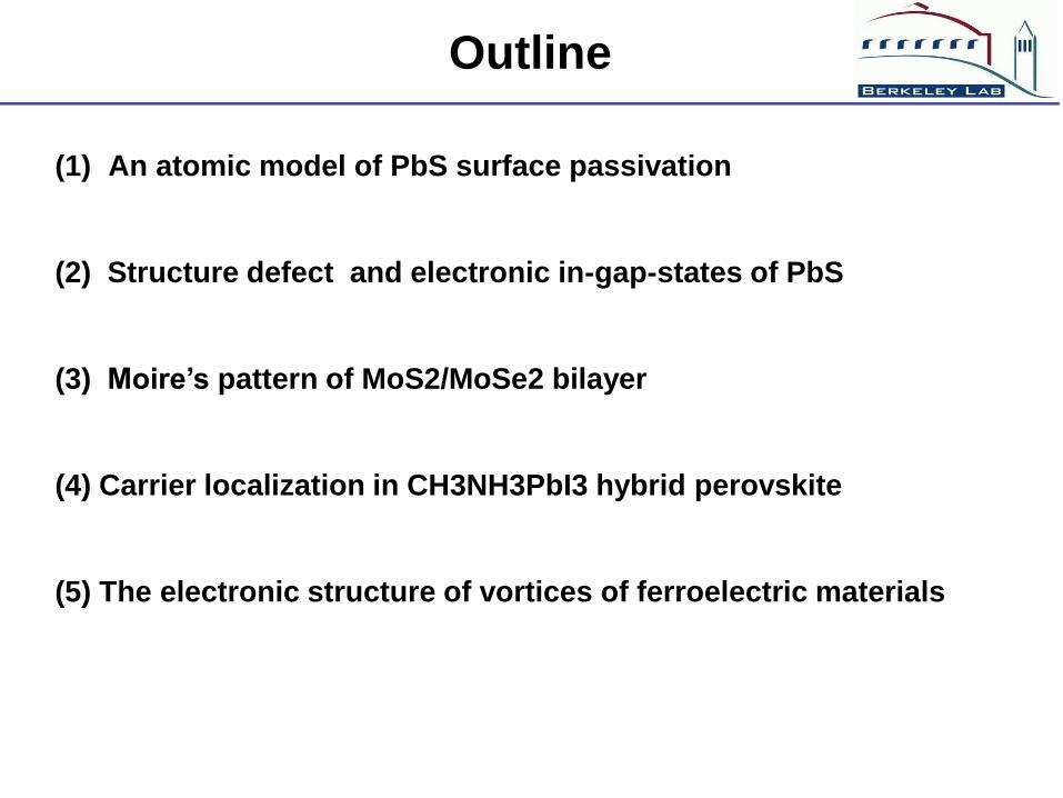
Outline
(1) An atomic model of PbS surface passivation
(2) Structure defect and electronic in-gap-states of PbS
(3) Moire’s pattern of MoS2/MoSe2 bilayer
(4) Carrier localization in CH3NH3PbI3 hybrid perovskite
(5) The electronic structure of vortices of ferroelectric materials
Outline
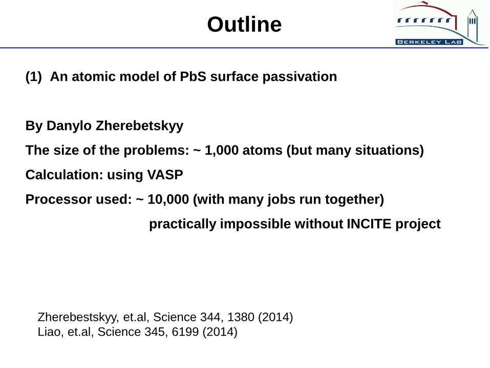
(1) An atomic model of PbS surface passivation
By Danylo Zherebetskyy
The size of the problems: ~ 1,000 atoms (but many situations)
Calculation: using VASP
Processor used: ~ 10,000 (with many jobs run together)
practically impossible without INCITE project
Zherebestskyy, et.al, Science 344, 1380 (2014)
Liao, et.al, Science 345, 6199 (2014)
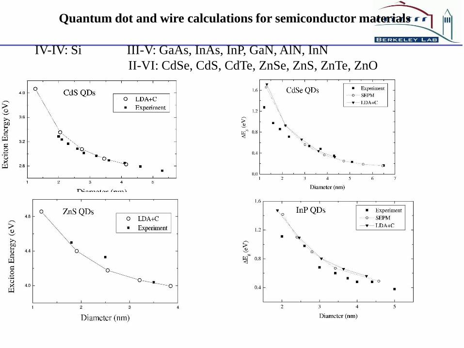
Quantum dot and wire calculations for semiconductor materials
IV-IV: Si III-V: GaAs, InAs, InP, GaN, AlN, InN
II-VI: CdSe, CdS, CdTe, ZnSe, ZnS, ZnTe, ZnO
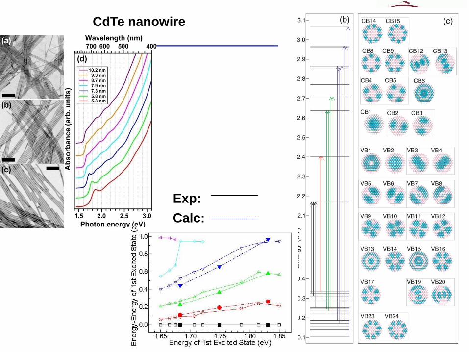
CdTe nanowire
Exp:
Calc:
All the previous calculations are assuming
perfect surface passivation
But what about realistic surface passivation?
Many problems are related to surface passivation
Hot carrier cooling
Carrier transport between QD
Efficiency of PL
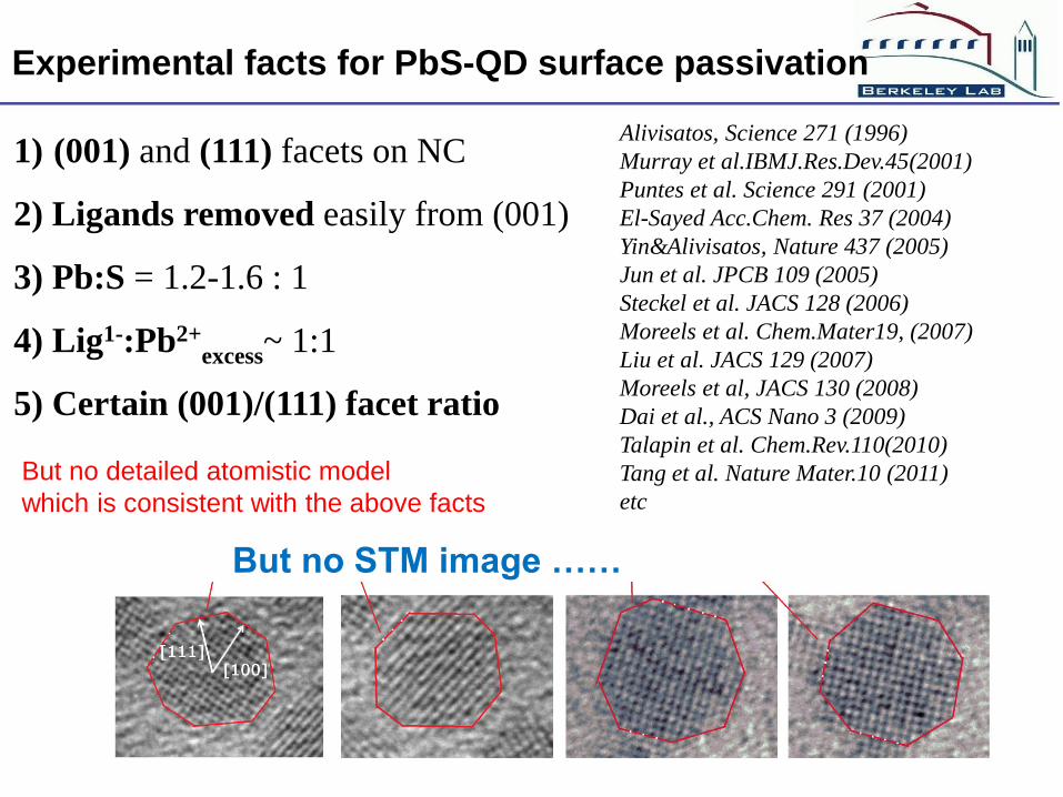
1) (001) and (111) facets on NC
2) Ligands removed easily from (001)
3) Pb:S = 1.2-1.6 : 1
4) Lig1-:Pb2+excess
~ 1:1
5) Certain (001)/(111) facet ratio
Alivisatos, Science 271 (1996)
Murray et al.IBMJ.Res.Dev.45(2001)
Puntes et al. Science 291 (2001)
El-Sayed Acc.Chem. Res 37 (2004)
Yin&Alivisatos, Nature 437 (2005)
Jun et al. JPCB 109 (2005)
Steckel et al. JACS 128 (2006)
Moreels et al. Chem.Mater19, (2007)
Liu et al. JACS 129 (2007)
Moreels et al, JACS 130 (2008)
Dai et al., ACS Nano 3 (2009)
Talapin et al. Chem.Rev.110(2010)
Tang et al. Nature Mater.10 (2011)
etc
But no detailed atomistic model
which is consistent with the above facts
Experimental facts for PbS-QD surface passivation
But no STM image ……
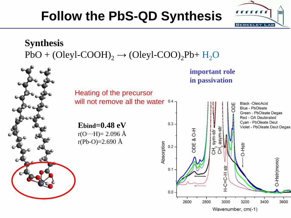
Follow the PbS-QD Synthesis
Ebind=0.48 eV r(O···H)= 2.096 Å
r(Pb-O)=2.690 Å
important role
in passivation
Synthesis
PbO + (Oleyl-COOH)2 → (Oleyl-COO)2Pb+ H2O
Heating of the precursor
will not remove all the water
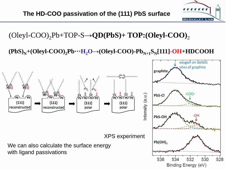
(PbS)N+(Oleyl-COO)2Pb···H2O→(Oleyl-COO)-PbN+1SN[111]-OH+HDCOOH
The HD-COO passivation of the (111) PbS surface
XPS experiment
(Oleyl-COO)2Pb+TOP-S→QD(PbS)+ TOP:(Oleyl-COO)2
We can also calculate the surface energy
with ligand passivations
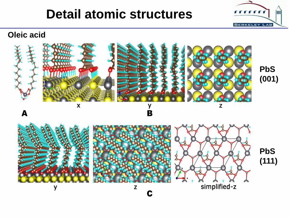
Detail atomic structures
Oleic acid
PbS
(001)
PbS
(111)
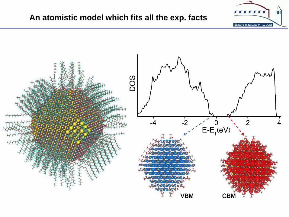
An atomistic model which fits all the exp. facts
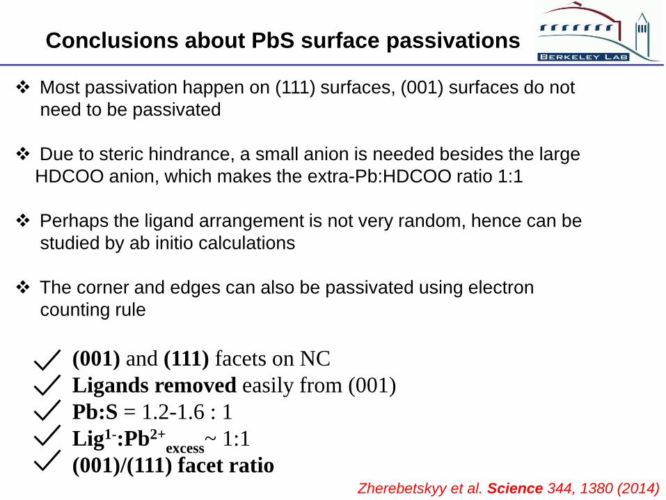
Conclusions about PbS surface passivations
Most passivation happen on (111) surfaces, (001) surfaces do not
need to be passivated
Due to steric hindrance, a small anion is needed besides the large
HDCOO anion, which makes the extra-Pb:HDCOO ratio 1:1
Perhaps the ligand arrangement is not very random, hence can be
studied by ab initio calculations
The corner and edges can also be passivated using electron
counting rule
Zherebetskyy et al. Science 344, 1380 (2014)
(001) and (111) facets on NC
Ligands removed easily from (001)
Pb:S = 1.2-1.6 : 1
Lig1-:Pb2+excess
~ 1:1
(001)/(111) facet ratio
Outline
(2) Structure defect and electronic in-gap-states of PbS
Danylo Zhevebetskyy
Size of the problems: ~1,000 atoms (but many situations)
Calculation: using VASP
Processor used: ~ 10,000 (with many jobs run together)
practically impossible without INCITE project
Question:
Does the QD surface have to be so perfect
in order to have good electronic and optical properties?
It is almost impossible to have such perfect surfaces!
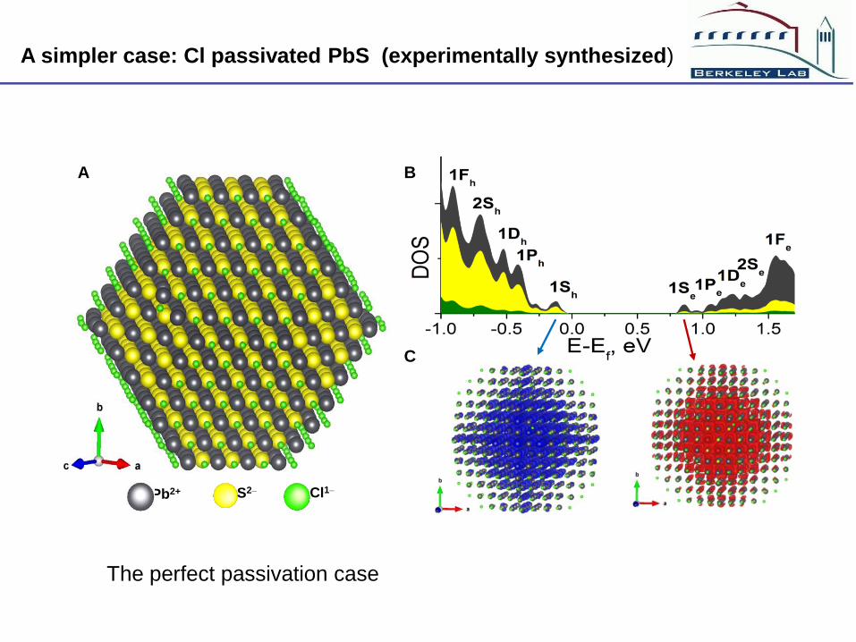
Pb2+ Cl1– S2–
A B
C
A simpler case: Cl passivated PbS (experimentally synthesized)
The perfect passivation case
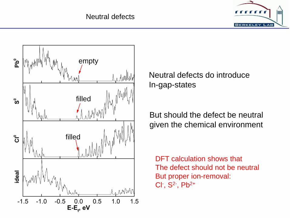
Neutral defects
Neutral defects do introduce
In-gap-states
empty
filled
filled
But should the defect be neutral
given the chemical environment
DFT calculation shows that
The defect should not be neutral
But proper ion-removal:
Cl-, S2-, Pb2+
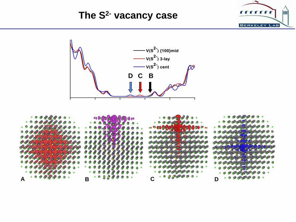
D
E
A
B
C
IGS
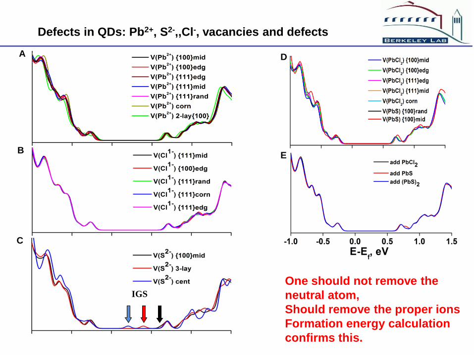
One should not remove the
neutral atom,
Should remove the proper ions
Formation energy calculation
confirms this.
Defects in QDs: Pb2+, S2-,,Cl-, vacancies and defects
A B C D
B C D
The S2- vacancy case
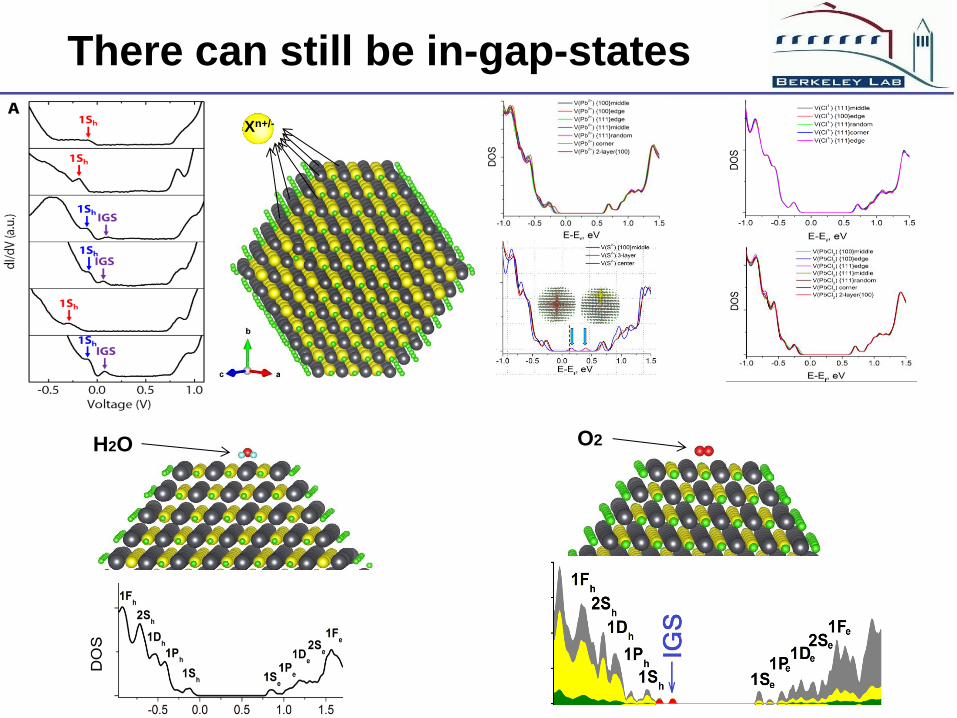
There can still be in-gap-states
Xn+/-
H2O O2
Conclusion about the defects
One must remove the proper ions, not neutral atoms
(the calculation shows the proper ion defects have lower formation E).
Most proper ion defects do not induce electronic in-gap state
S2- at the interior of the QD does induce defect state, but there
is a large energy drive (0.9 eV) to drives the S2- out, and the
barrier is low (< 1 eV - tens of seconds).
The experimental observed surface trap state comes from surface
absorbed molecules.
Outline
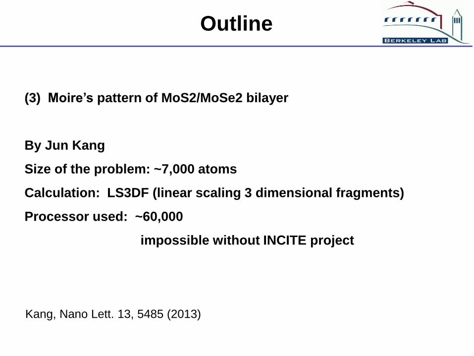
(3) Moire’s pattern of MoS2/MoSe2 bilayer
By Jun Kang
Size of the problem: ~7,000 atoms
Calculation: LS3DF (linear scaling 3 dimensional fragments)
Processor used: ~60,000
impossible without INCITE project
Kang, Nano Lett. 13, 5485 (2013)
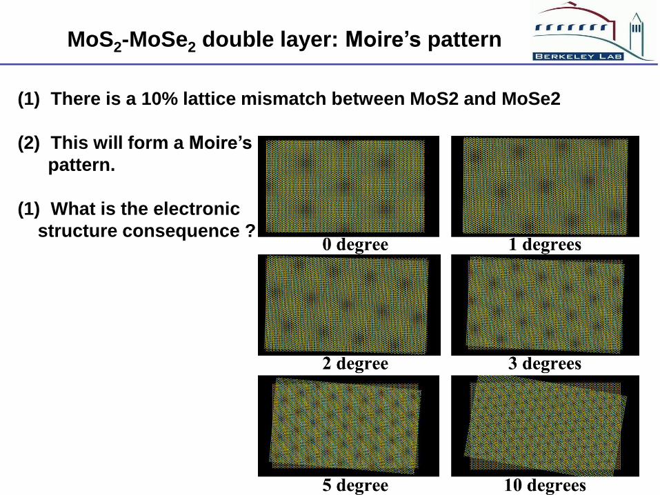
(1) There is a 10% lattice mismatch between MoS2 and MoSe2
(2) This will form a Moire’s
pattern.
(1) What is the electronic
structure consequence ?
MoS2-MoSe2 double layer: Moire’s pattern
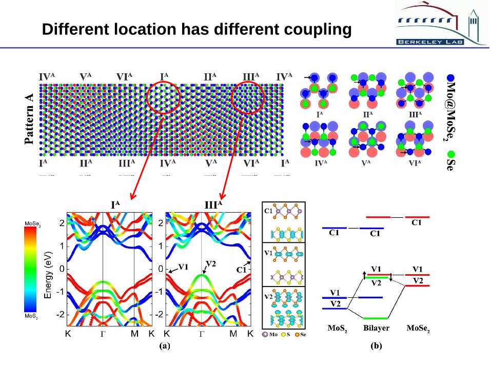
Different location has different coupling
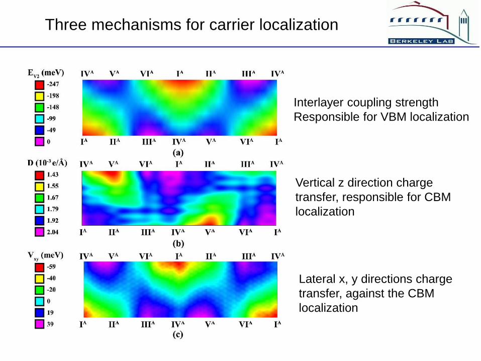
Three mechanisms for carrier localization
Interlayer coupling strength
Responsible for VBM localization
Vertical z direction charge
transfer, responsible for CBM
localization
Lateral x, y directions charge
transfer, against the CBM
localization
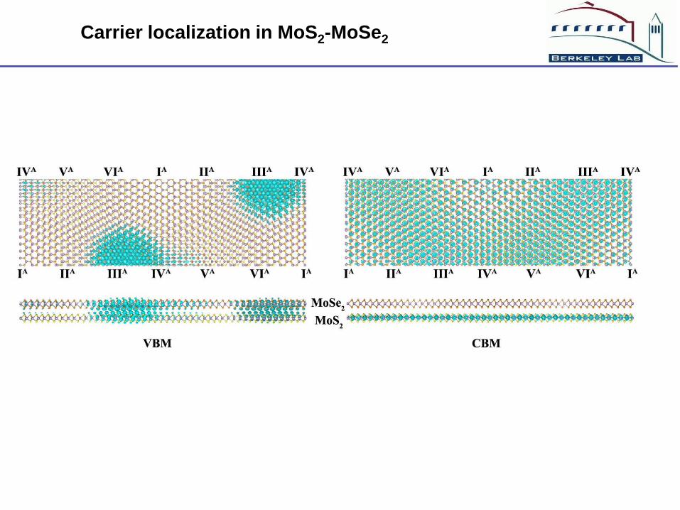
Carrier localization in MoS2-MoSe2
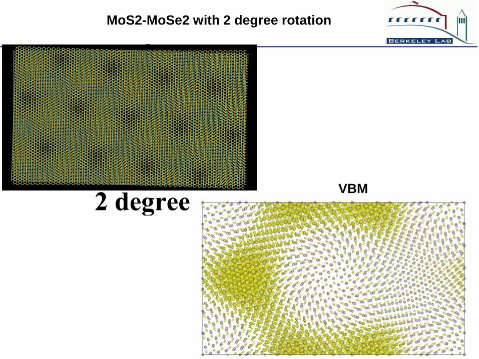
MoS2-MoSe2 with 2 degree rotation
VBM
Conclusions for MoS2/MoSe2 carrier localization
(1) The atomic Moire’s pattern will cause carrier localization
(2) The VBM is localized mostly by interlayer coupling
(3) The CBM is localized mostly by interlayer charge transfer
Outline
(4) Carrier localization in CH3NH3PbI3 hybrid perovskite
By Jie Ma
Size of the problem: ~20,000 atoms
Calculation: LS3DF (linear scaling 3 dimensional fragments)
Processor used: ~60,000
impossible without INCITE project
Ma and Wang, Nano Lett. 15, 248 (2015)
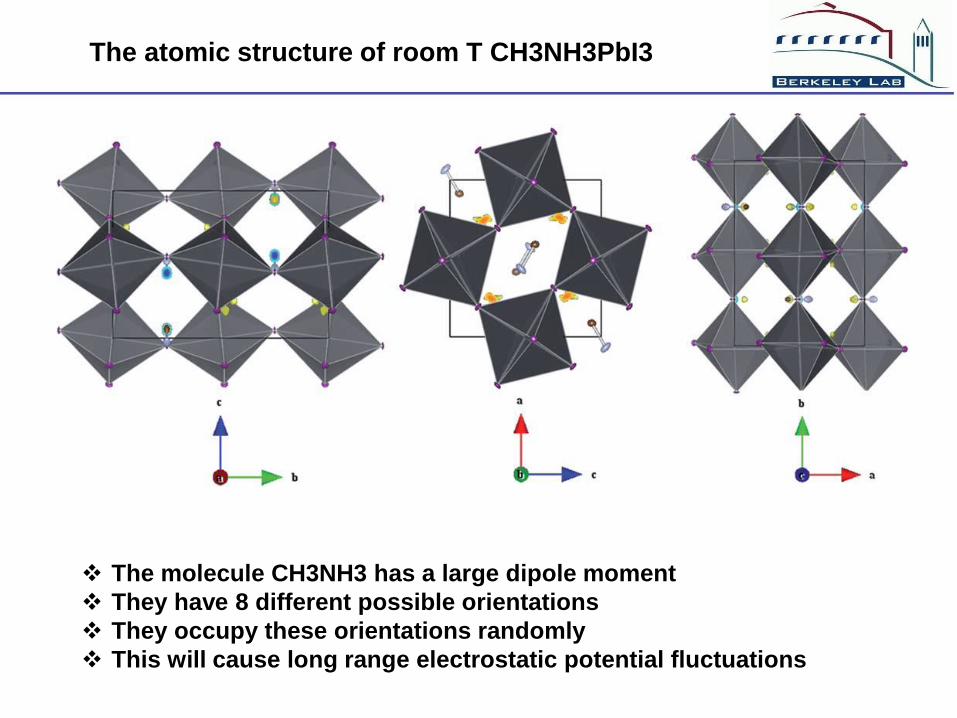
The atomic structure of room T CH3NH3PbI3
The molecule CH3NH3 has a large dipole moment
They have 8 different possible orientations
They occupy these orientations randomly
This will cause long range electrostatic potential fluctuations
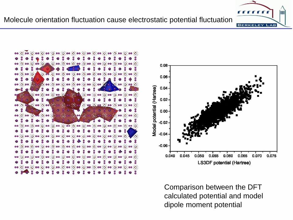
Comparison between the DFT
calculated potential and model
dipole moment potential
Molecule orientation fluctuation cause electrostatic potential fluctuation
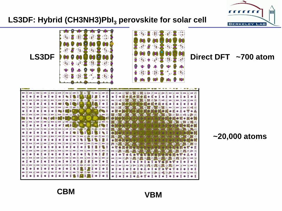
LS3DF: Hybrid (CH3NH3)PbI3 perovskite for solar cell
CBM VBM
~20,000 atoms
LS3DF Direct DFT ~700 atom
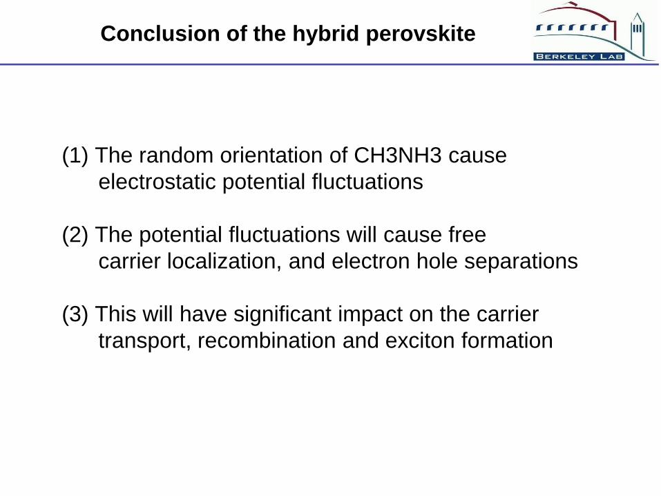
Conclusion of the hybrid perovskite
(1) The random orientation of CH3NH3 cause
electrostatic potential fluctuations
(2) The potential fluctuations will cause free
carrier localization, and electron hole separations
(3) This will have significant impact on the carrier
transport, recombination and exciton formation
Outline
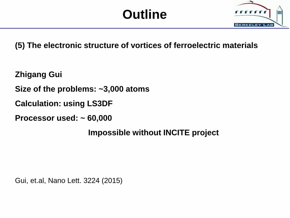
(5) The electronic structure of vortices of ferroelectric materials
Zhigang Gui
Size of the problems: ~3,000 atoms
Calculation: using LS3DF
Processor used: ~ 60,000
Impossible without INCITE project
Gui, et.al, Nano Lett. 3224 (2015)
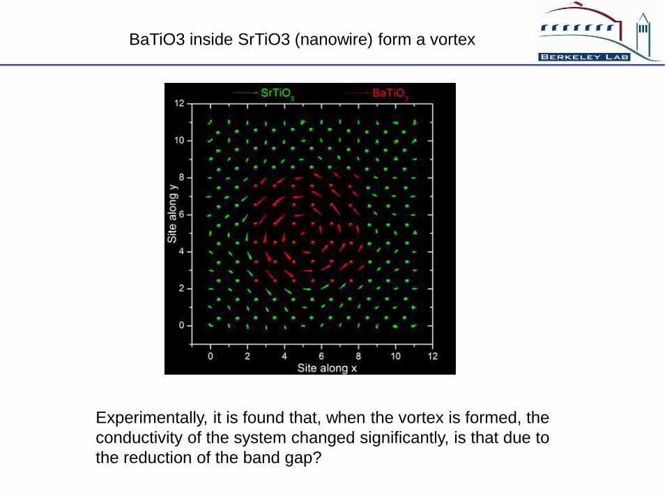
BaTiO3 inside SrTiO3 (nanowire) form a vortex
Experimentally, it is found that, when the vortex is formed, the
conductivity of the system changed significantly, is that due to
the reduction of the band gap?
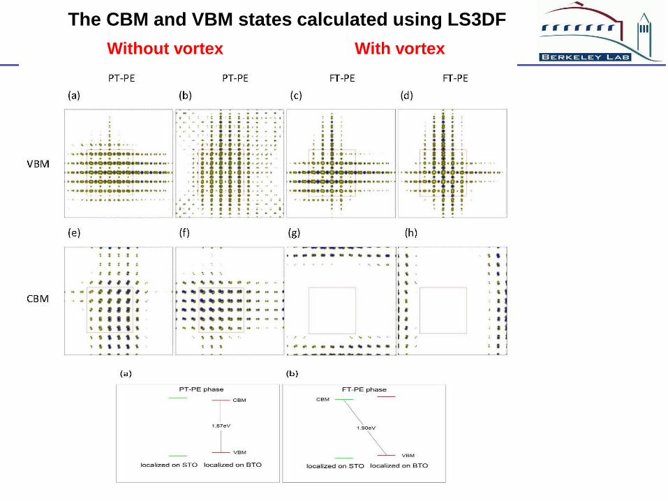
The CBM and VBM states calculated using LS3DF
With vortex Without vortex
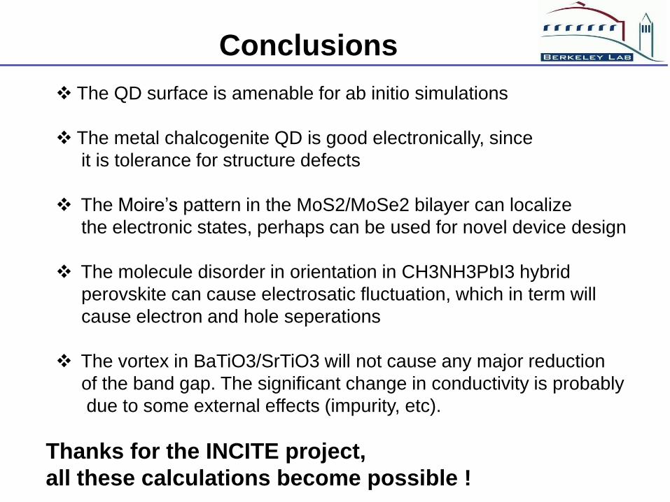
Conclusions
The QD surface is amenable for ab initio simulations
The metal chalcogenite QD is good electronically, since
it is tolerance for structure defects
The Moire’s pattern in the MoS2/MoSe2 bilayer can localize
the electronic states, perhaps can be used for novel device design
The molecule disorder in orientation in CH3NH3PbI3 hybrid
perovskite can cause electrosatic fluctuation, which in term will
cause electron and hole seperations
The vortex in BaTiO3/SrTiO3 will not cause any major reduction
of the band gap. The significant change in conductivity is probably
due to some external effects (impurity, etc).
Thanks for the INCITE project,
all these calculations become possible !