Embed Size (px)
Citation preview
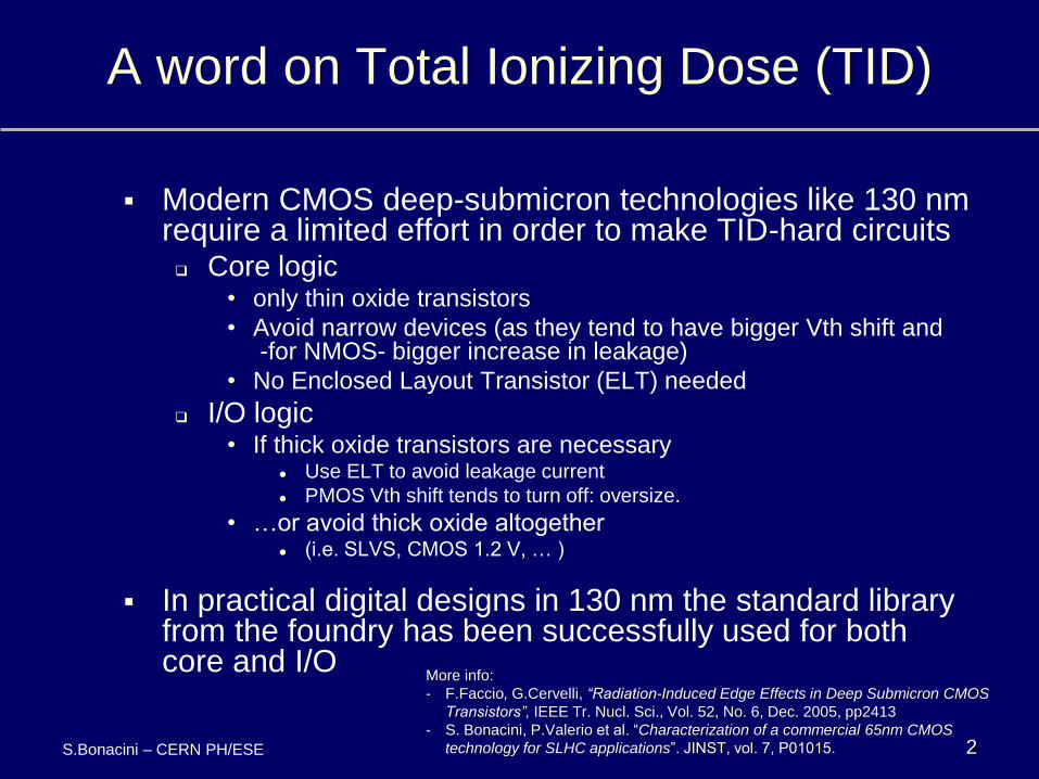
A word on Total Ionizing Dose (TID)
Modern CMOS deep-submicron technologies like 130 nm require a limited effort in order to make TID-hard circuits Core logic
• only thin oxide transistors
• Avoid narrow devices (as they tend to have bigger Vth shift and -for NMOS- bigger increase in leakage)
• No Enclosed Layout Transistor (ELT) needed
I/O logic • If thick oxide transistors are necessary
Use ELT to avoid leakage current
PMOS Vth shift tends to turn off: oversize.
• …or avoid thick oxide altogether (i.e. SLVS, CMOS 1.2 V, … )
In practical digital designs in 130 nm the standard library from the foundry has been successfully used for both core and I/O
S.Bonacini – CERN PH/ESE 2
More info:
- F.Faccio, G.Cervelli, “Radiation-Induced Edge Effects in Deep Submicron CMOS
Transistors”, IEEE Tr. Nucl. Sci., Vol. 52, No. 6, Dec. 2005, pp2413
- S. Bonacini, P.Valerio et al. “Characterization of a commercial 65nm CMOS
technology for SLHC applications”. JINST, vol. 7, P01015.
SEU risk management
3 S.Bonacini – CERN PH/ESE
SEU is not a destructive event
a given rate can be tolerated (depending on the system)
How often does it happen? Depends on:
Radiation environment
Which particles?
Which energy?
Which fluence?
Device sensitivity
The “safer” the circuit is designed, the more “expensive” it is (area, performance, complexity, …)
Risk reduction comes at some cost
4
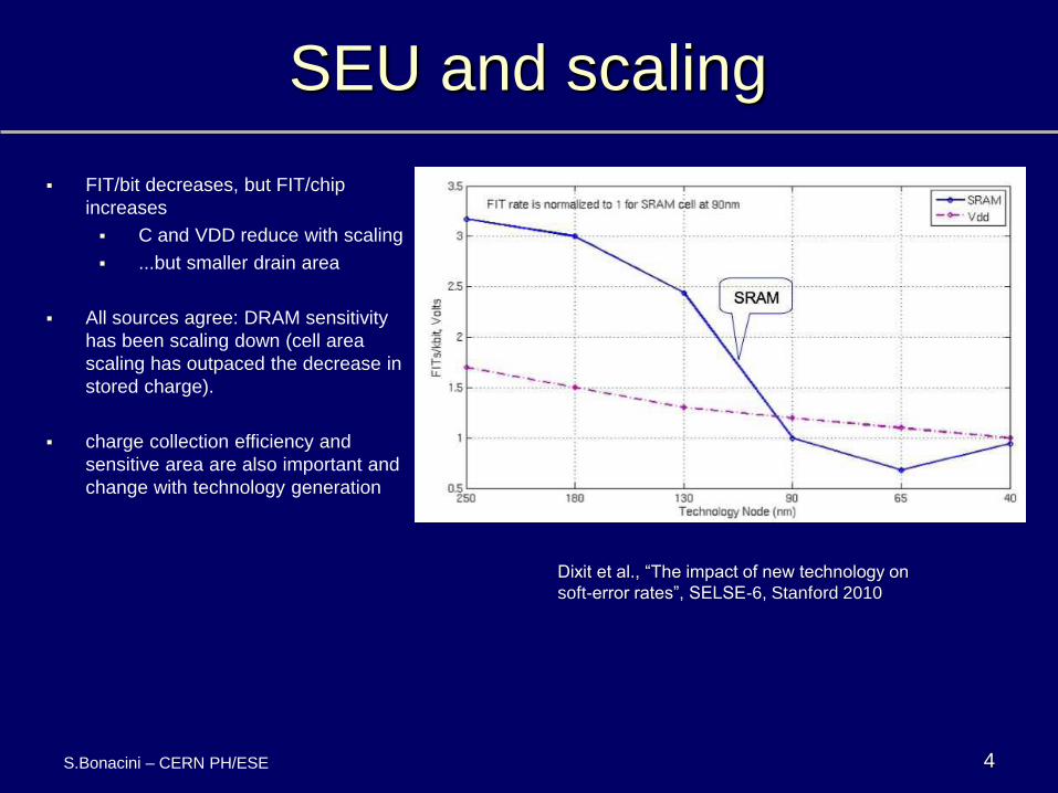
SEU and scaling
Dixit et al., “The impact of new technology on
soft-error rates”, SELSE-6, Stanford 2010
FIT/bit decreases, but FIT/chip
increases
C and VDD reduce with scaling
...but smaller drain area
All sources agree: DRAM sensitivity
has been scaling down (cell area
scaling has outpaced the decrease in
stored charge).
charge collection efficiency and
sensitive area are also important and
change with technology generation
S.Bonacini – CERN PH/ESE
5
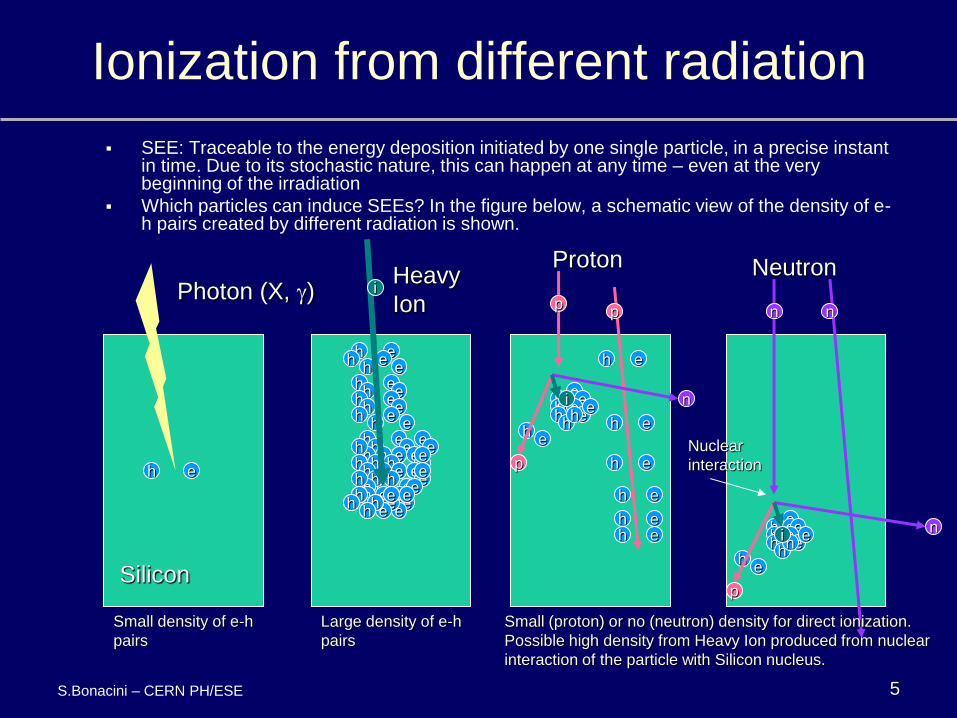
Ionization from different radiation
SEE: Traceable to the energy deposition initiated by one single particle, in a precise instant in time. Due to its stochastic nature, this can happen at any time – even at the very beginning of the irradiation
Which particles can induce SEEs? In the figure below, a schematic view of the density of e-h pairs created by different radiation is shown.
Heavy
Ion
e h e h
e h
e h
e h e h e h
e h e h
e h e h
e h e h
e h h h h
e e e
e e e e
e h h h
h h h h
h h h
h h h h
e
e
e e e e
e e e
h e h h h
h h e e e
e e e e e
h h h h h h
i Neutron
n
e h e h
e h e
h e h
e h
e h
p
n i
n
Proton
e h
e h
e h
e h
e h e h
p
e h e h
e h e
h e h
e h
e h
p
n i
p
Small density of e-h
pairs
Large density of e-h
pairs
Small (proton) or no (neutron) density for direct ionization.
Possible high density from Heavy Ion produced from nuclear
interaction of the particle with Silicon nucleus.
Photon (X, g)
e h
Silicon
Nuclear
interaction
S.Bonacini – CERN PH/ESE
6
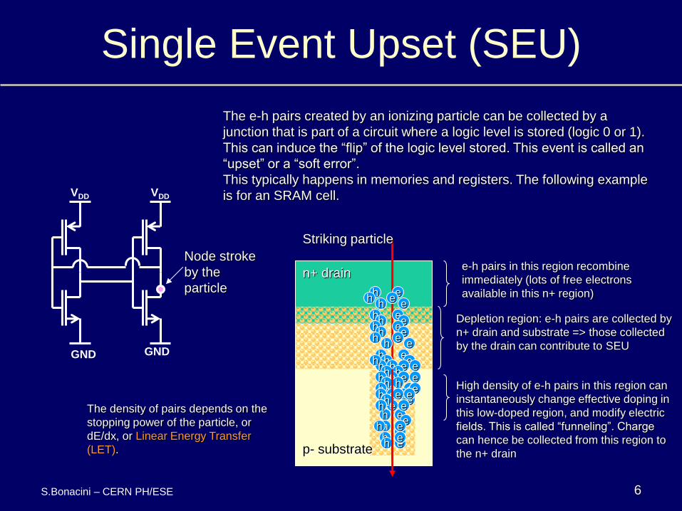
Single Event Upset (SEU)
The e-h pairs created by an ionizing particle can be collected by a
junction that is part of a circuit where a logic level is stored (logic 0 or 1).
This can induce the “flip” of the logic level stored. This event is called an
“upset” or a “soft error”.
This typically happens in memories and registers. The following example
is for an SRAM cell.
GND GND
VDD VDD
Node stroke
by the
particle
p- substrate
Striking particle
Depletion region: e-h pairs are collected by
n+ drain and substrate => those collected
by the drain can contribute to SEU
n+ drain e-h pairs in this region recombine
immediately (lots of free electrons
available in this n+ region)
High density of e-h pairs in this region can
instantaneously change effective doping in
this low-doped region, and modify electric
fields. This is called “funneling”. Charge
can hence be collected from this region to
the n+ drain
S.Bonacini – CERN PH/ESE
e h e h
e h
e h
e h e h e h
e h e h
e h e h
e h e h
e h
h
h
h
e e
e
e
e e e
e
h h h
h h h h
h h h
h
h h h
e
e
e e e
e
e
e e
h e h
h h h
h
e e e e
e e e
h h h h h h The density of pairs depends on the
stopping power of the particle, or
dE/dx, or Linear Energy Transfer
(LET).
7
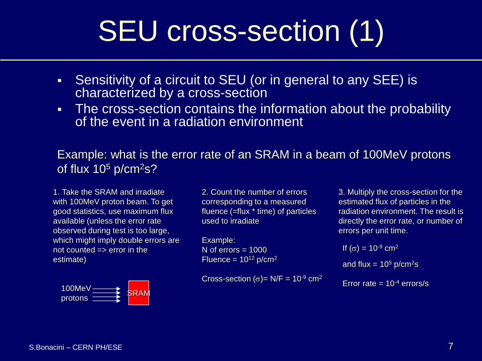
SEU cross-section (1)
Sensitivity of a circuit to SEU (or in general to any SEE) is characterized by a cross-section
The cross-section contains the information about the probability of the event in a radiation environment
Example: what is the error rate of an SRAM in a beam of 100MeV protons
of flux 105 p/cm2s?
1. Take the SRAM and irradiate
with 100MeV proton beam. To get
good statistics, use maximum flux
available (unless the error rate
observed during test is too large,
which might imply double errors are
not counted => error in the
estimate)
SRAM 100MeV
protons
2. Count the number of errors
corresponding to a measured
fluence (=flux * time) of particles
used to irradiate
Example:
N of errors = 1000
Fluence = 1012 p/cm2
Cross-section (s)= N/F = 10-9 cm2
3. Multiply the cross-section for the
estimated flux of particles in the
radiation environment. The result is
directly the error rate, or number of
errors per unit time.
If (s) = 10-9 cm2
and flux = 105 p/cm2s
Error rate = 10-4 errors/s
S.Bonacini – CERN PH/ESE
8
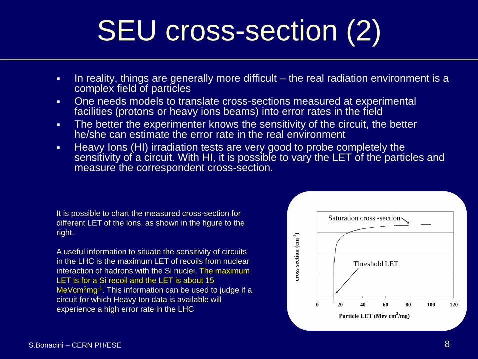
SEU cross-section (2)
In reality, things are generally more difficult – the real radiation environment is a complex field of particles
One needs models to translate cross-sections measured at experimental facilities (protons or heavy ions beams) into error rates in the field
The better the experimenter knows the sensitivity of the circuit, the better he/she can estimate the error rate in the real environment
Heavy Ions (HI) irradiation tests are very good to probe completely the sensitivity of a circuit. With HI, it is possible to vary the LET of the particles and measure the correspondent cross-section.
It is possible to chart the measured cross-section for
different LET of the ions, as shown in the figure to the
right.
A useful information to situate the sensitivity of circuits
in the LHC is the maximum LET of recoils from nuclear
interaction of hadrons with the Si nuclei. The maximum
LET is for a Si recoil and the LET is about 15
MeVcm2mg-1. This information can be used to judge if a
circuit for which Heavy Ion data is available will
experience a high error rate in the LHC
0 20 40 60 80 100 120
Particle LET (Mev cm 2 /mg) or proton energy (MeV)
cross
sec
tion
(cm
2 )
Saturation cross - section
Threshold LET
0 20 40 60 80 100 120
Particle LET (Mev cm 2 /mg) or proton energy (MeV)
cross
sec
tion
(cm
2 )
0 20 40 60 80 100 120
Particle LET (Mev cm 2 /mg)
cross
sec
tion
(cm
2 )
Saturation cross - section
Threshold LET
S.Bonacini – CERN PH/ESE
9
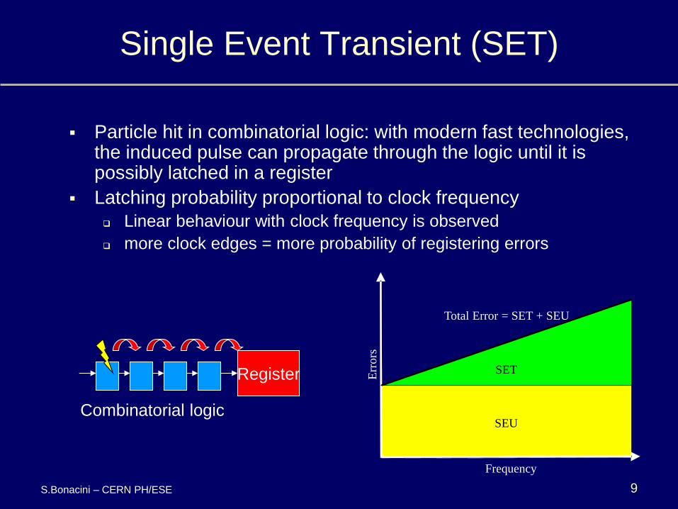
Single Event Transient (SET)
Particle hit in combinatorial logic: with modern fast technologies, the induced pulse can propagate through the logic until it is possibly latched in a register
Latching probability proportional to clock frequency
Linear behaviour with clock frequency is observed
more clock edges = more probability of registering errors
SET
SEU
Total Error = SET + SEU
Err
ors
Frequency
Register
Combinatorial logic
S.Bonacini – CERN PH/ESE
P-sub
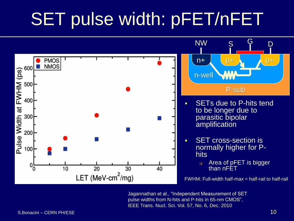
SET pulse width: pFET/nFET
SETs due to P-hits tend to be longer due to parasitic bipolar amplification
SET cross-section is normally higher for P-hits Area of pFET is bigger
than nFET
10
Jagannathan et al., “Independent Measurement of SET
pulse widths from N-hits and P-hits in 65-nm CMOS”,
IEEE Trans. Nucl. Sci. Vol. 57, No. 6, Dec. 2010
FWHM: Full-width half-max = half-rail to half-rail
S.Bonacini – CERN PH/ESE
n-well
p+ p+ n+
S D G NW
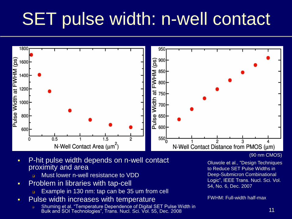
SET pulse width: n-well contact
P-hit pulse width depends on n-well contact proximity and area Must lower n-well resistance to VDD
Problem in libraries with tap-cell Example in 130 nm: tap can be 35 um from cell
Pulse width increases with temperature Shuming et al. “Temperature Dependence of Digital SET Pulse Width in
Bulk and SOI Technologies”, Trans. Nucl. Sci. Vol. 55, Dec. 2008 11
Oluwole et al., “Design Techniques
to Reduce SET Pulse Widths in
Deep-Submicron Combinational
Logic”, IEEE Trans. Nucl. Sci. Vol.
54, No. 6, Dec. 2007
FWHM: Full-width half-max
(90 nm CMOS)
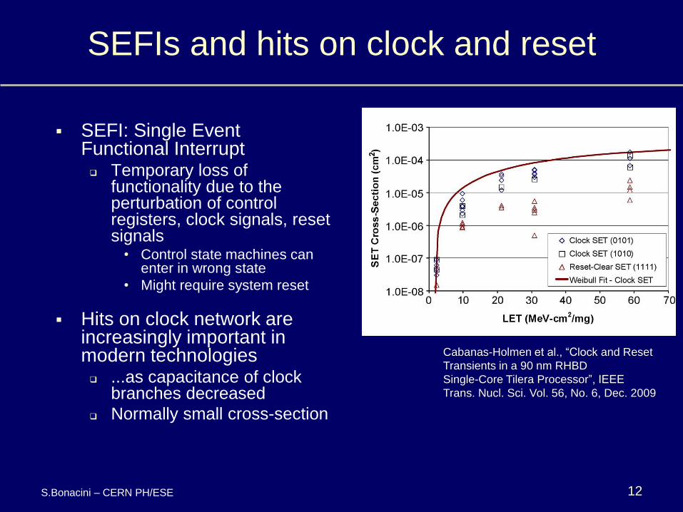
SEFIs and hits on clock and reset
SEFI: Single Event Functional Interrupt Temporary loss of
functionality due to the perturbation of control registers, clock signals, reset signals
• Control state machines can enter in wrong state
• Might require system reset
Hits on clock network are increasingly important in modern technologies ...as capacitance of clock
branches decreased
Normally small cross-section
12
Cabanas-Holmen et al., “Clock and Reset
Transients in a 90 nm RHBD
Single-Core Tilera Processor”, IEEE
Trans. Nucl. Sci. Vol. 56, No. 6, Dec. 2009
S.Bonacini – CERN PH/ESE
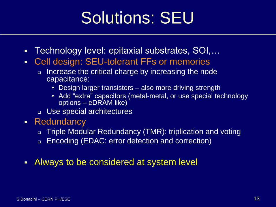
Solutions: SEU
Technology level: epitaxial substrates, SOI,…
Cell design: SEU-tolerant FFs or memories Increase the critical charge by increasing the node
capacitance: • Design larger transistors – also more driving strength
• Add “extra” capacitors (metal-metal, or use special technology options – eDRAM like)
Use special architectures
Redundancy Triple Modular Redundancy (TMR): triplication and voting
Encoding (EDAC: error detection and correction)
Always to be considered at system level
13 S.Bonacini – CERN PH/ESE
14
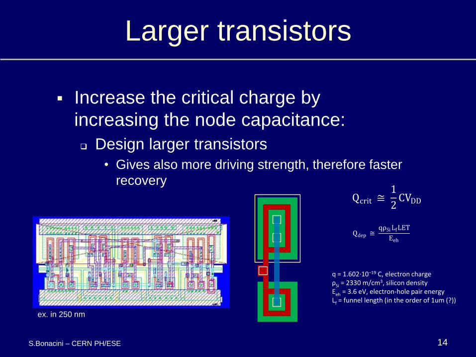
Larger transistors
Increase the critical charge by
increasing the node capacitance:
Design larger transistors
• Gives also more driving strength, therefore faster
recovery
S.Bonacini – CERN PH/ESE
ex. in 250 nm
q = 1.602·10−19 C, electron charge
ρSi = 2330 m/cm3, silicon density
Eeh = 3.6 eV, electron-hole pair energy
Lf = funnel length (in the order of 1um (?))
Qcrit ≅ 1
2CVDD
Qdep ≅ qρSi LfLET
Eeh
15
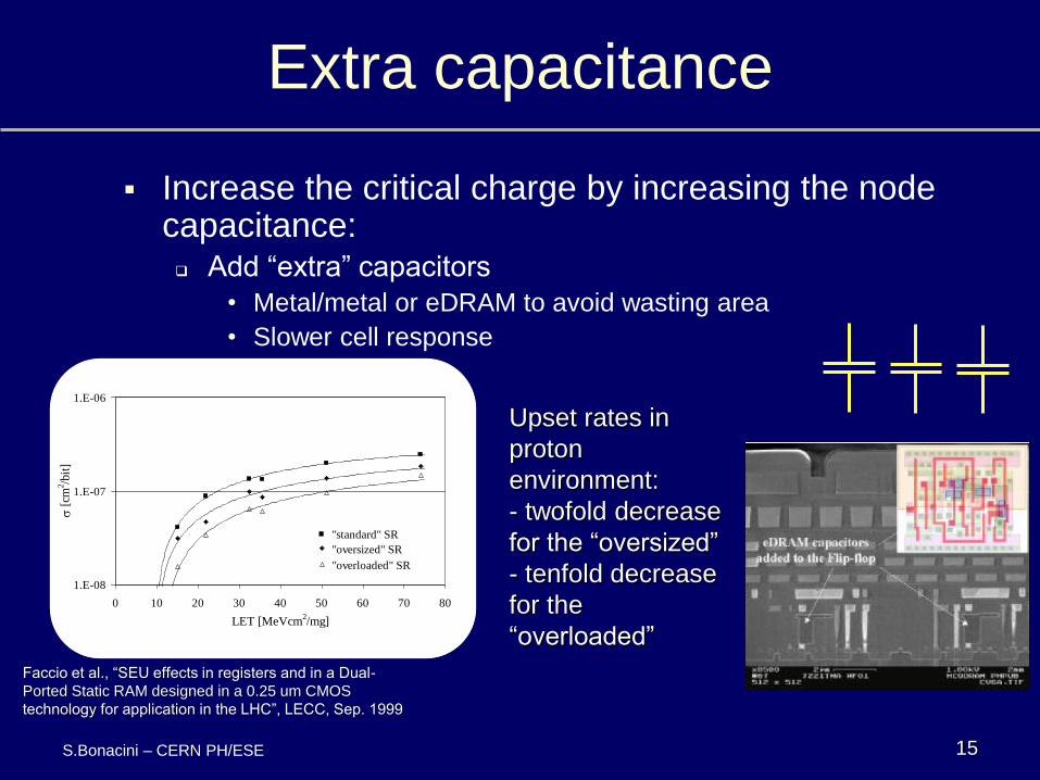
Extra capacitance
Increase the critical charge by increasing the node capacitance: Add “extra” capacitors
• Metal/metal or eDRAM to avoid wasting area
• Slower cell response
1.E-08
1.E-07
1.E-06
0 10 20 30 40 50 60 70 80
LET [MeVcm2/mg]
s [
cm2/b
it]
"standard" SR
"oversized" SR
"overloaded" SR
Upset rates in
proton
environment:
- twofold decrease
for the “oversized”
- tenfold decrease
for the
“overloaded”
S.Bonacini – CERN PH/ESE
Faccio et al., “SEU effects in registers and in a Dual-
Ported Static RAM designed in a 0.25 um CMOS
technology for application in the LHC”, LECC, Sep. 1999
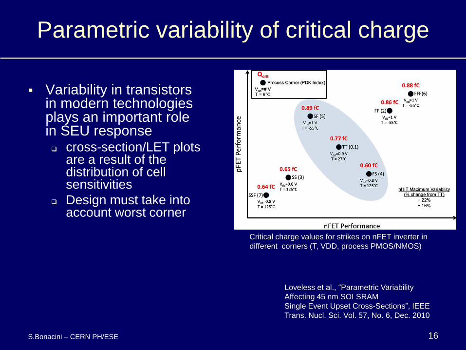
Parametric variability of critical charge
Variability in transistors in modern technologies plays an important role in SEU response cross-section/LET plots
are a result of the distribution of cell sensitivities
Design must take into account worst corner
16
Loveless et al., “Parametric Variability
Affecting 45 nm SOI SRAM
Single Event Upset Cross-Sections”, IEEE
Trans. Nucl. Sci. Vol. 57, No. 6, Dec. 2010
Critical charge values for strikes on nFET inverter in
different corners (T, VDD, process PMOS/NMOS)
S.Bonacini – CERN PH/ESE
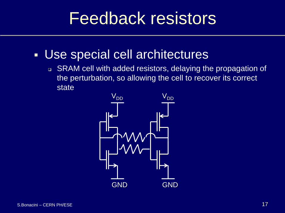
Feedback resistors
Use special cell architectures SRAM cell with added resistors, delaying the propagation of
the perturbation, so allowing the cell to recover its correct
state
GND
VDD
GND
VDD
17 S.Bonacini – CERN PH/ESE
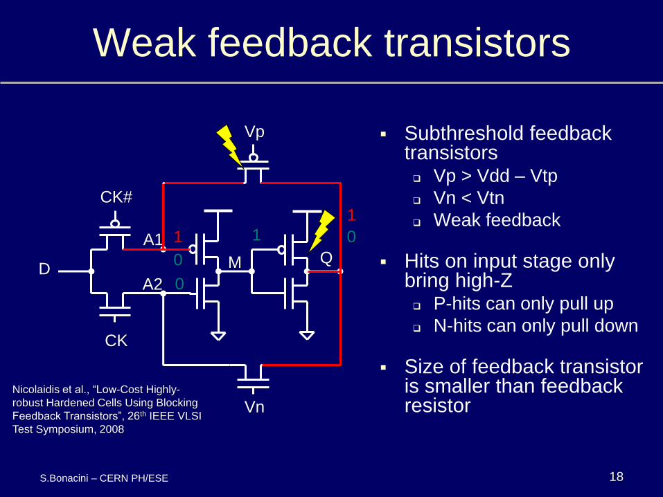
Weak feedback transistors
Subthreshold feedback transistors Vp > Vdd – Vtp
Vn < Vtn
Weak feedback
Hits on input stage only bring high-Z P-hits can only pull up
N-hits can only pull down
Size of feedback transistor is smaller than feedback resistor
18
Nicolaidis et al., “Low-Cost Highly-
robust Hardened Cells Using Blocking
Feedback Transistors”, 26th IEEE VLSI
Test Symposium, 2008
D
CK#
CK
Vp
Vn
Q A1
A2
M
S.Bonacini – CERN PH/ESE
0
1
1
0
0
1
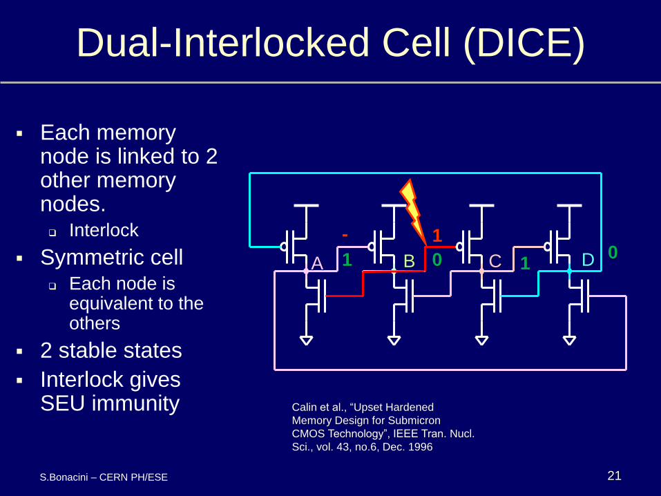
Dual-Interlocked Cell (DICE)
Each memory node is linked to 2 other memory nodes. Interlock
Symmetric cell Each node is
equivalent to the others
2 stable states
Interlock gives SEU immunity
21
1 1 0 0
1 -
A B C D
Calin et al., “Upset Hardened
Memory Design for Submicron
CMOS Technology”, IEEE Tran. Nucl.
Sci., vol. 43, no.6, Dec. 1996
S.Bonacini – CERN PH/ESE
22
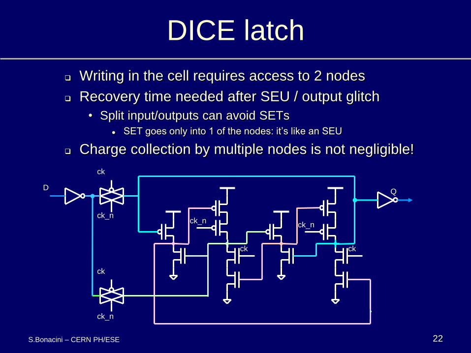
DICE latch
ck
ck
ck_n
ck_n
ck
ck_n
ck
ck_n
D0
D1
Q0
Q1
Writing in the cell requires access to 2 nodes
Recovery time needed after SEU / output glitch
• Split input/outputs can avoid SETs
SET goes only into 1 of the nodes: it’s like an SEU
Charge collection by multiple nodes is not negligible!
S.Bonacini – CERN PH/ESE
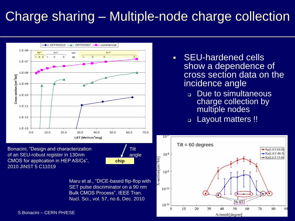
Charge sharing – Multiple-node charge collection
SEU-hardened cells show a dependence of cross section data on the incidence angle Due to simultaneous
charge collection by multiple nodes
Layout matters !!
23
Maru et al., “DICE-based flip-flop with
SET pulse discriminator on a 90 nm
Bulk CMOS Process”, IEEE Tran.
Nucl. Sci., vol. 57, no.6, Dec. 2010
1.E-13
1.E-12
1.E-11
1.E-10
1.E-09
1.E-08
1.E-07
1.E-06
0.0 10.0 20.0 30.0 40.0 50.0 60.0 70.0
LET [MeVcm2/mg]
Cro
ss s
ecti
on
[cm
2/b
it]
DFFR2010 DFFR2007 commercial
Kr25+Ne7+ Ar10+
0° 45°
60°
0° 45°
60°
0° 30°
45°
60°
ion
tilt
Bonacini, “Design and characterization
of an SEU-robust register in 130nm
CMOS for application in HEP ASICs”,
2010 JINST 5 C11019
S.Bonacini – CERN PH/ESE
Tilt = 60 degrees
chip
Tilt
angle
Layouts for SEU-hard FFs
Sensitive nodes of latch must be separated the more distance, the less probability of charge-sharing
waste of area?
A possible solution is interleaving master and slave nodes of a D-FF…. or even nodes from several D-FFs!
Dense interconnect !
24
10 um
S0
C
Q0
a
S1
C
Q1
a
M0D
CK
0a
S0D M1D
CK
1a
S1D
M0
A
S0
A
Q0
b
M1
A
S1
A
Q1
b
M0B
CK
0b
S0B M1B
CK
1b
S1B M
0C
M1
C
minimum distance 4.5 μm
1x D-FF in 250 nm tech.
2x D-FF in 130 nm tech.
Bonacini et al., “An SEU-Robust
Configurable Logic Block for the
Implementation of a Radiation-
Tolerant FPGA”, Trans. Nucl. Sci.,
vol. 53, no. 6, Dec. 2006
Up to level 3 metal used fully for internal cell interconnect
Less routing resources for cell-to-cell wiring
S.Bonacini – CERN PH/ESE
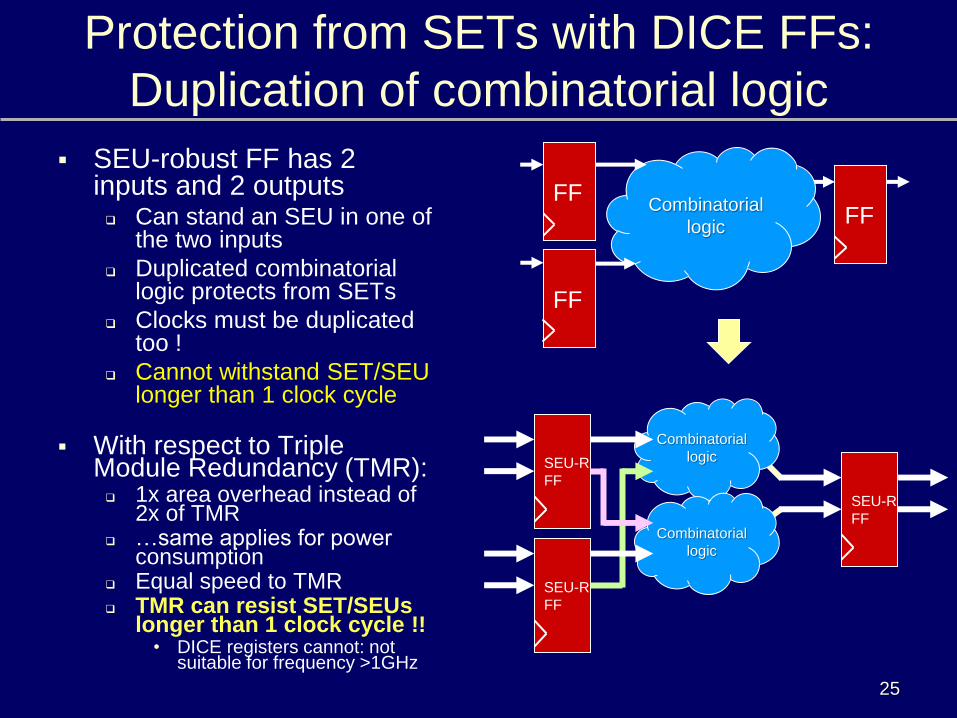
Protection from SETs with DICE FFs:
Duplication of combinatorial logic
SEU-robust FF has 2 inputs and 2 outputs Can stand an SEU in one of
the two inputs
Duplicated combinatorial logic protects from SETs
Clocks must be duplicated too !
Cannot withstand SET/SEU longer than 1 clock cycle
With respect to Triple Module Redundancy (TMR): 1x area overhead instead of
2x of TMR …same applies for power
consumption Equal speed to TMR TMR can resist SET/SEUs
longer than 1 clock cycle !! • DICE registers cannot: not
suitable for frequency >1GHz
25
FF FF
FF
Combinatorial
logic
SEU-R
FF
SEU-R
FF
SEU-R
FF
Combinatorial
logic
Combinatorial
logic
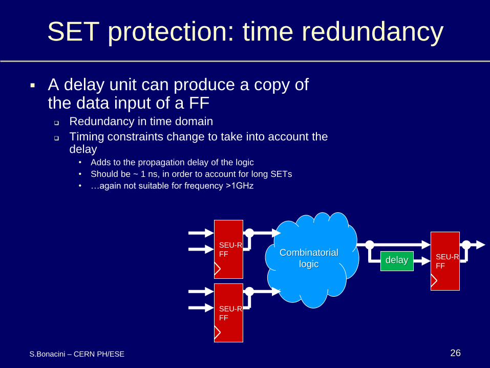
SET protection: time redundancy
26
SEU-R
FF SEU-R
FF
SEU-R
FF
Combinatorial
logic delay
A delay unit can produce a copy of the data input of a FF Redundancy in time domain
Timing constraints change to take into account the delay
• Adds to the propagation delay of the logic
• Should be ~ 1 ns, in order to account for long SETs
• …again not suitable for frequency >1GHz
S.Bonacini – CERN PH/ESE
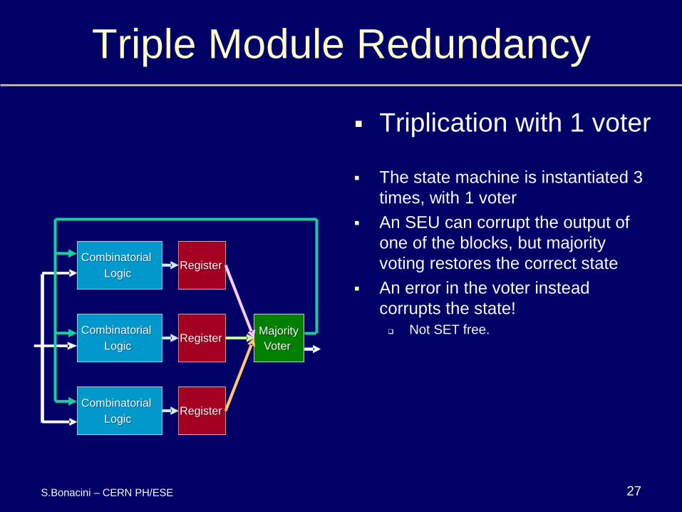
Triple Module Redundancy
Triplication with 1 voter
The state machine is instantiated 3
times, with 1 voter
An SEU can corrupt the output of
one of the blocks, but majority
voting restores the correct state
An error in the voter instead
corrupts the state! Not SET free.
27
Combinatorial
Logic
Combinatorial
Logic
Combinatorial
Logic
Register
Register
Register
Majority
Voter
Combinatorial
Logic
Combinatorial
Logic
Combinatorial
Logic
Register
Register
Register
S.Bonacini – CERN PH/ESE
30
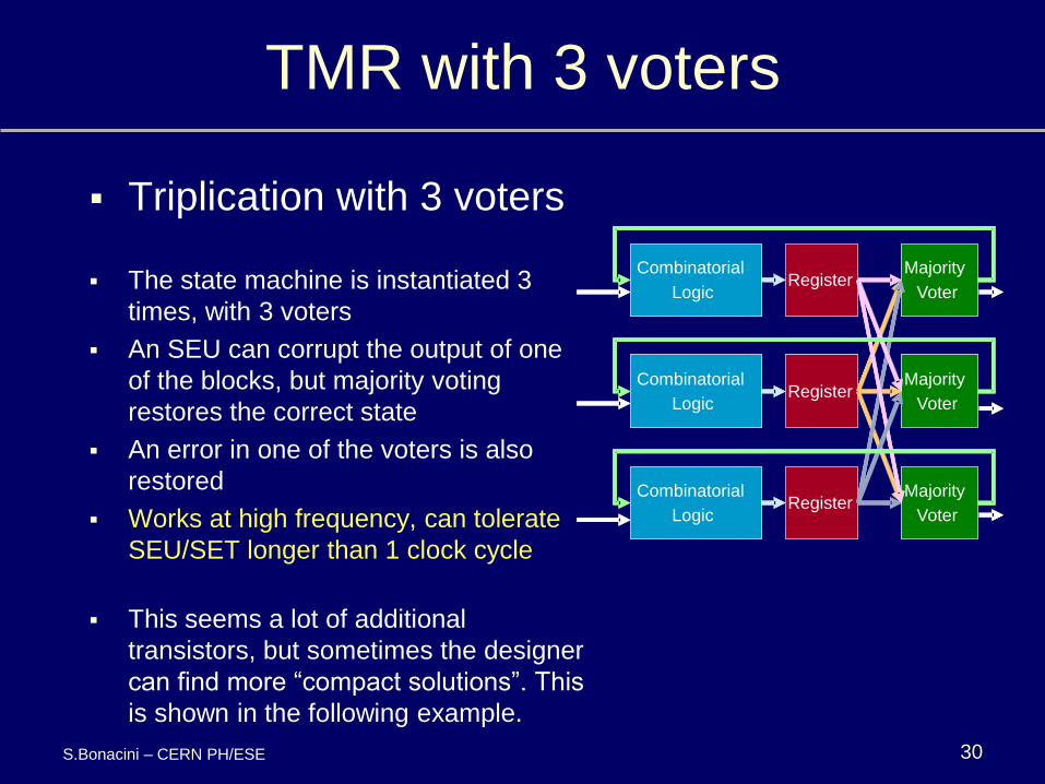
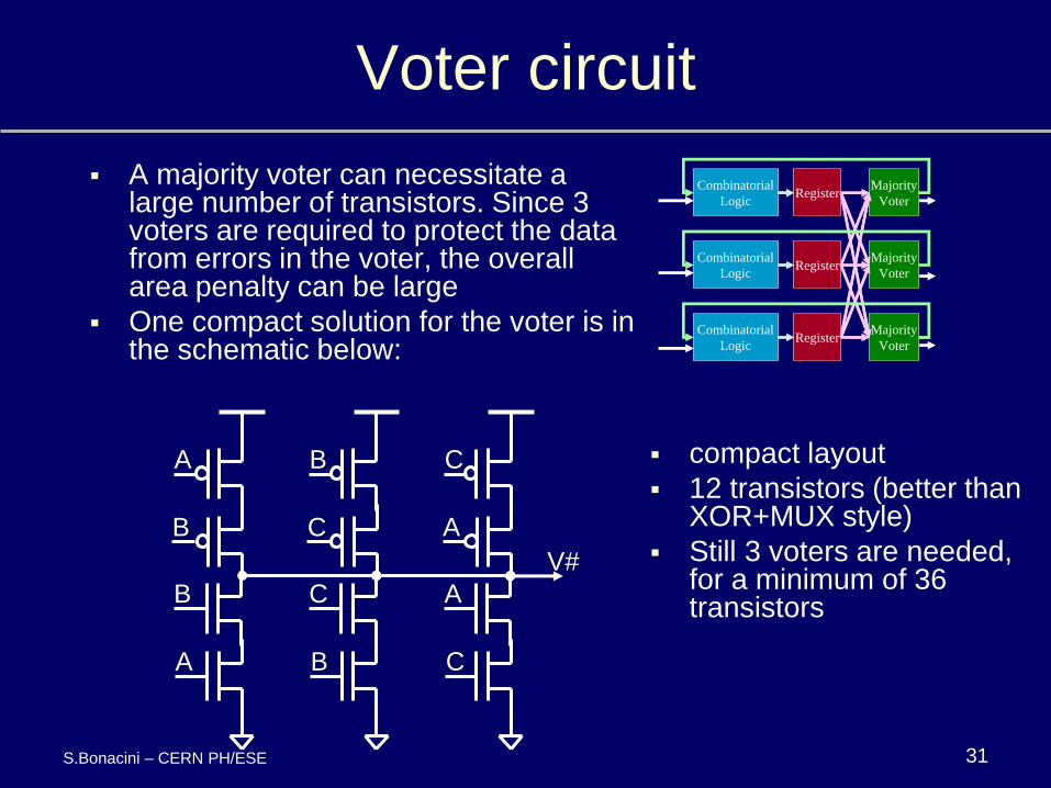
TMR with 3 voters
Triplication with 3 voters
The state machine is instantiated 3
times, with 3 voters
An SEU can corrupt the output of one
of the blocks, but majority voting
restores the correct state
An error in one of the voters is also
restored
Works at high frequency, can tolerate
SEU/SET longer than 1 clock cycle
This seems a lot of additional
transistors, but sometimes the designer
can find more “compact solutions”. This
is shown in the following example.
Combinatorial
Logic
Combinatorial
Logic
Combinatorial
Logic
Register
Register
Register
Majority
Voter
Majority
Voter
Majority
Voter
Combinatorial
Logic
Combinatorial
Logic
Combinatorial
Logic
Register
Register
Register
Majority
Voter
Majority
Voter
Majority
Voter
S.Bonacini – CERN PH/ESE
31
Voter circuit
A majority voter can necessitate a large number of transistors. Since 3 voters are required to protect the data from errors in the voter, the overall area penalty can be large
One compact solution for the voter is in the schematic below:
Combinatorial
Logic
Combinatorial
Logic
Combinatorial
Logic
Register
Register
Register
Majority
Voter
Majority
Voter
Majority
Voter
Combinatorial
Logic
Combinatorial
Logic
Combinatorial
Logic
Register
Register
Register
Majority
Voter
Majority
Voter
Majority
Voter
B
B
A
A
C
C
B
B
A
A
C
C
V#
compact layout
12 transistors (better than XOR+MUX style)
Still 3 voters are needed, for a minimum of 36 transistors
S.Bonacini – CERN PH/ESE
32
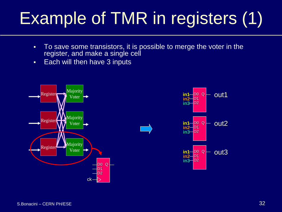
Example of TMR in registers (1)
To save some transistors, it is possible to merge the voter in the register, and make a single cell
Each will then have 3 inputs
Register
Register
Register
Majority
Voter
Majority
Voter
Majority
Voter
D0 D1 D2
Q
ck
D0 D1 D2
Q in1 in2 in3
out1
out2
out3
D0 D1 D2
Q in1 in2 in3
D0 D1 D2
Q in1 in2 in3
S.Bonacini – CERN PH/ESE
33
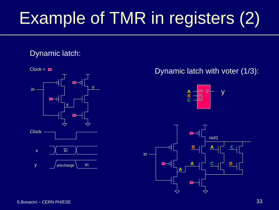
Example of TMR in registers (2)
in
Clock =
x
y
x
Clock
y
in
in precharge
Dynamic latch:
D0 D1 D2
Q A B C
y
out1
in
A
A
A B
B C
C
Dynamic latch with voter (1/3):
S.Bonacini – CERN PH/ESE
34
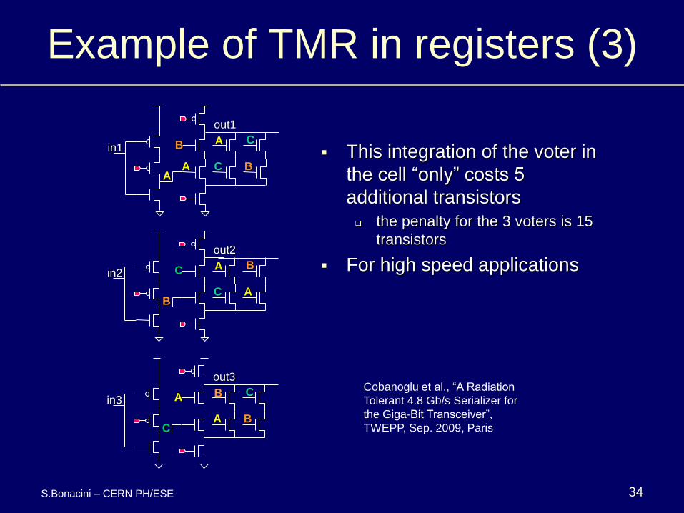
Example of TMR in registers (3)
out1
in1
A A
A B
B C
C
out2
in2
B
A C
A C
B
out3
in3
C
B A
B A
C
This integration of the voter in
the cell “only” costs 5
additional transistors
the penalty for the 3 voters is 15
transistors
For high speed applications
Cobanoglu et al., “A Radiation
Tolerant 4.8 Gb/s Serializer for
the Giga-Bit Transceiver”,
TWEPP, Sep. 2009, Paris
S.Bonacini – CERN PH/ESE
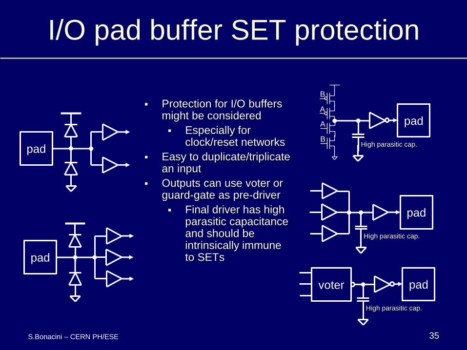
I/O pad buffer SET protection
pad
pad
pad
High parasitic cap.
pad
High parasitic cap.
voter
A
A
B
B
pad
High parasitic cap.
Protection for I/O buffers might be considered
Especially for clock/reset networks
Easy to duplicate/triplicate an input
Outputs can use voter or guard-gate as pre-driver
Final driver has high parasitic capacitance and should be intrinsically immune to SETs
S.Bonacini – CERN PH/ESE 35
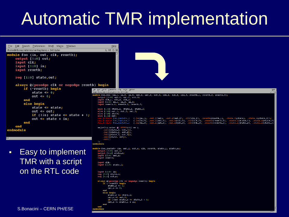
Automatic TMR implementation
36
Easy to implement
TMR with a script
on the RTL code
S.Bonacini – CERN PH/ESE
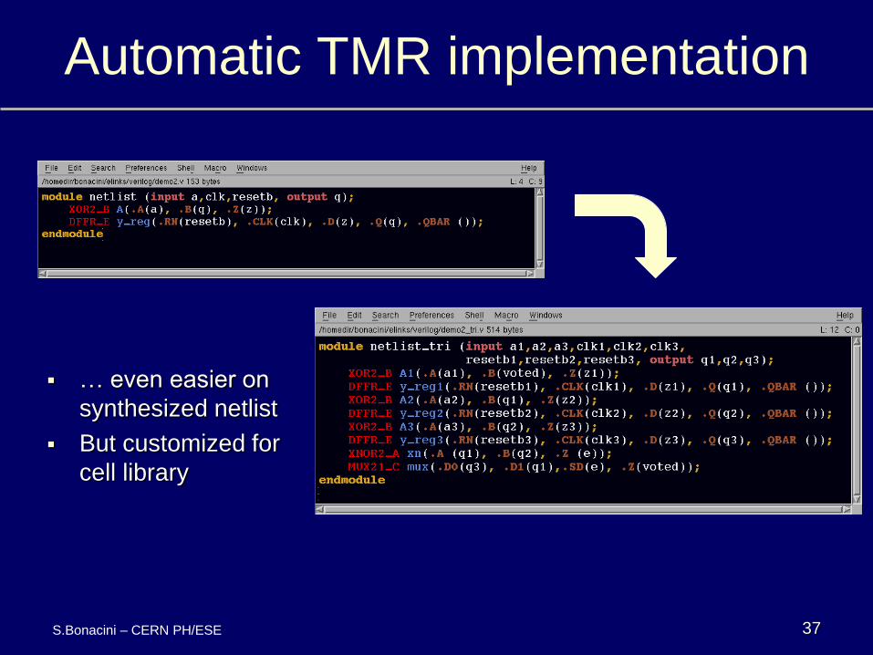
Automatic TMR implementation
37
… even easier on
synthesized netlist
But customized for
cell library
S.Bonacini – CERN PH/ESE
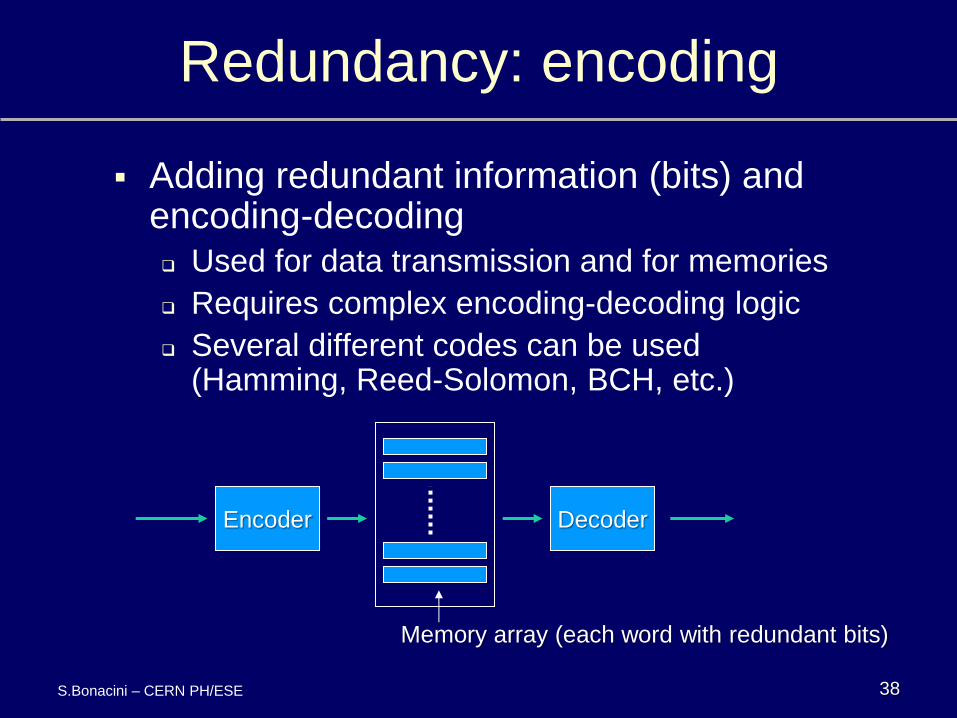
Redundancy: encoding
Adding redundant information (bits) and encoding-decoding Used for data transmission and for memories
Requires complex encoding-decoding logic
Several different codes can be used (Hamming, Reed-Solomon, BCH, etc.)
Encoder Decoder
Memory array (each word with redundant bits)
38 S.Bonacini – CERN PH/ESE
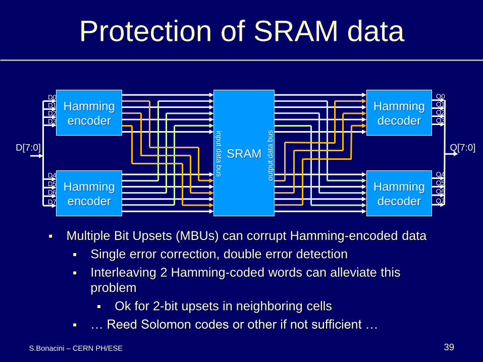
Protection of SRAM data
S.Bonacini – CERN PH/ESE 39
Hamming
encoder
Hamming
encoder
D0
SRAM
Hamming
decoder
Hamming
decoder
D[7:0]
D1
D2
D3
D4
D5
D6
D7
Q0
Q1
Q2
Q3
Q4
Q5
Q6
Q7
Q[7:0]
Multiple Bit Upsets (MBUs) can corrupt Hamming-encoded data
Single error correction, double error detection
Interleaving 2 Hamming-coded words can alleviate this
problem
Ok for 2-bit upsets in neighboring cells
… Reed Solomon codes or other if not sufficient …
inpu
t data
bus
outp
ut d
ata
bus
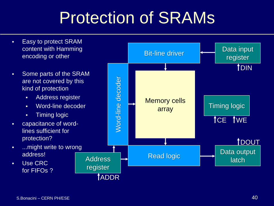
Protection of SRAMs
40
Bit-line driver
Read logic
Word
-lin
e d
ecoder
Address
register
Data input
register
Data output
latch
Timing logic Memory cells
array
ADDR
DIN
DOUT
WE CE
Easy to protect SRAM
content with Hamming
encoding or other
Some parts of the SRAM
are not covered by this
kind of protection
Address register
Word-line decoder
Timing logic
capacitance of word-
lines sufficient for
protection?
...might write to wrong
address!
Use CRC
for FIFOs ?
S.Bonacini – CERN PH/ESE
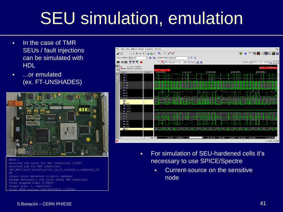
SEU simulation, emulation
41 S.Bonacini – CERN PH/ESE
In the case of TMR
SEUs / fault injections
can be simulated with
HDL
...or emulated
(ex. FT-UNSHADES)
#RUN 1
Selected clk cycle for SEU insertion: 133937
Selected reg for SEU insertion:
SEU_MUT/leon0_mcore0_proc0_cx.c0_icache0_r.waddress_16
OK
Output error detected in port: address
Damage detected 1 clk cycle after SEU insertion
Total elapsed time: 0.06251
Target size: 1, registers
Total FPGA cycles: 0x0,00020B32 <133938>
For simulation of SEU-hardened cells it’s
necessary to use SPICE/Spectre
Current-source on the sensitive
node
Further reading
General material on radiation effects: The best source is the “archive of Radiation Effects Short Course Notebooks, 1980-2002” collecting the courses given at
the IEEE NSREC conference (CD sold by IEEE)
On SEU-tolerant Cells: Increased capacitance:
• F.Faccio et al., “Single Event Effects in Static and Dynamic Registers in a 0.25mm CMOS Technology”, IEEE Trans. Nucl. Science, Vol.46, No.6, pp.1434-1439, December 1999
• F.Faccio et al., “SEU effects in registers and in a Dual-Ported Static RAM designed in a 0.25mm CMOS technology for applications in the LHC”, in the proceedings of the Fifth Workshop on Electronics for LHC Experiments, Snowmass, September 20-24, 1999, pp.571-575 (CERN 99-09, CERN/LHCC/99-33, 29 October 1999)
• P.Roche, F.Jacquet, C.Caillat, J.P.Schoellkopf, "An Alpha Immune and Ultra Low Neutron SER High Density SRAM", proceedings of IRPS 2004, pp671-672, April 2004
• Calin et al., “Upset Hardened Memory Design for Submicron CMOS Technology”, IEEE Tran. Nucl. Sci., vol. 43, no.6, Dec. 1996
• Bonacini, “Design and characterization of an SEU-robust register in 130nm CMOS for application in HEP ASICs”, 2010 JINST 5 C11019
• Bonacini et al., “An SEU-Robust Configurable Logic Block for the Implementation of a Radiation-Tolerant FPGA”, Trans. Nucl. Sci., vol. 53, no. 6, Dec. 2006
• Nicolaidis et al., “Low-Cost Highly-robust Hardened Cells Using Blocking Feedback Transistors”, 26th IEEE VLSI Test Symposium, 2008
• Bessot, Velazco, “Design of SEU-Hardened CMOS Memory Cells: the HIT Cell”, RADECS, Sep. 1993
• Liu & Whitaker, “Low Power SEU Immune CMOS Memory Circuits”, IEEE Trans. Nucl. Sci., vol. 39, no. 6, Dec, 1992
On TMR and encoding: Paper comparing techniques and containing references, to be used as a starting research point: S.Niranjan, J.F.Frenzel,
“A comparison of Fault-Tolerant State Machine Architectures for Space-Borne Electronics”, IEEE Trans. On Reliability, Vol.45, No1, p.109, March 1996
42 S.Bonacini – CERN PH/ESE