Embed Size (px)
Citation preview
Large-Area Wet Micro-Printing (LAMP) for Organic Device Patterning
Hongzheng Jin1,2 and James C. Sturm1,2 1 Department of Electrical Engineering, Princeton University, Princeton, NJ 08544, USA 2 Princeton Institute for the Science and Technology of Materials (PRISM), Princeton University, Princeton, NJ 08544, USA
ABSTRACT
An important challenge for Organic Light-Emitting Diodes (OLEDs) manufacturing is the patterning method of the organic materials used for different colors. In this talk, a Large-Area wet Micro-Printing (LAMP) technique is proposed and demonstrated for organic device patterning. A printing plate is first prepared by surface engineering so that a designed surface energy pattern is achieved. The printing plate is then coated with “ ink,” brought into contact with the device substrate, and the “ ink” is transferred. With this approach, the red (R), green (G) and blue (B) sub-pixel arrays needed in a full-color display can be printed in three successive steps, one step for each color. Both single-color pixel arrays and R, G, B sub-pixel arrays have been patterned as a demonstration of the feasibility of this method. The technique has the potential advantages of low-cost and high-throughput and it avoids some of the practical problems associated with the design and operation of an ink-jet apparatus. INTRODUCTION
In the fabrication of monochrome OLEDs, active materials are usually deposited by thermal evaporation for small molecules or by spin-coating for polymers. A full-color OLED, however, requires the patterning of different organic materials used for R, G, B sub-pixels. Patterning of small molecules can be achieved by thermal evaporation and shadow mask, while ink-jet printing [1,2] has been widely developed for polymers. Nevertheless, there are several shortcomings to ink-jet printing, such as nozzle clogging, repeatability of the direction of droplet travel, and throughput [2].
The approach demonstrated in this work is to print organic device layers from a wet solution not drop by drop, as in ink-jet printing, but rather over a large area at once using a patterned printing plate. We refer to the method as Large-Area wet Micro-Printing (LAMP). This method uses surface engineering techniques to pattern the surface energy of a printing plate and then uses the printing plate to locally deposit organic materials. Patterning of different color pixels for full-color OLED can be achieved by three successive printing steps.
Both single-color pixel arrays and R, G, B sub-pixel arrays are demonstrated. Monochrome OLED devices were tested for their electrical and electroluminescent properties. The printed devices show efficiencies somewhat lower than those by spin-coating. The results suggest that LAMP is a promising patterning technique for low-cost full-color OLED displays. EXPERIMENTAL DETAILS
The LAMP technique is illustrated schematically in Figure 1. A printing plate is first prepared by surface energy patterning (discussed below) so that a designed wettability pattern is
Mater. Res. Soc. Symp. Proc. Vol. 871E © 2005 Materials Research Society I6.27.1

Figure 1. Schematic diagram of Large-Area wet Micro-Printing (LAMP) technique for organic device patterning. a) a surface-energy-patterned printing plate is coated with red “ ink” ; b) the printing plate is brought into contact with the device plate, i.e., to print; c) the printing plate is separated from the device plate and the transferred “ ink” is allowed to dry; d,e) steps a-c are repeated for green and blue sub-pixels. achieved. The printing plate is then coated with “ ink” , a solvent solution with dissolved organic materials to be printed. Guided by the wettability pattern, ink sticks only to selected regions of the printing plate. The printing plate is then brought into contact with the device substrate, during which ink is transferred to desired locations. Following printing, the printing plate is separated from the contact with the device plate and the solvent is allowed to dry, leaving a patterned organic film on the target substrate. The concept is similar to that of Darhuber et al. [3] and Miller et al.[4], for printing single polymer layer, but differs in the fact that they printed polymers either in their precursor form [3] or above Tg [4], not polymers in solution.
In this work, 1H,1H,2H,2H-Perfluorooctyl-trichlorosilane (PFOTS, Purchased from Fluka) is used to adjust the surface energy of the printing plate [5]. PFOTS forms a self-assembled monolayer (SAM) on the surface of glass (or silicon substrate where a thin surface layer of silicon dioxide present). PFOTS has a very low critical surface tension [6], so that a PFOTS monolayer coated surface will be “ liquo-phobic” [5]. On the contrary, a clean silicon dioxide surface has a very high surface energy and is thus “ liquo-philic” for both water and many solvents.
The printing plate used here was prepared by combining photolithography with molecular self-assembly of the PFOTS. A silicon wafer is first patterned with a photoresist layer by conventional photolithography. The PFOTS growth on the wafer is done in a nitrogen glove box, where the wafer is immersed in anhydrous dodecane for five minutes. The plate is then placed into a solution of PFOTS in dodecane (a few mM) for five minutes. The plate is then removed from the solution and rinsed in de-ionized water and blown dry. PFOTS monolayer will form on the surface where there is no photoresist. Finally the photoresist is stripped by acetone in an ultrasonic bath. The printing plate is then finished, containing both liquophilic (clean surface region) and liquophobic (PFOTS-coated) regions.
An example of the printing plate prepared in this way is shown in Figure 2. The silicon wafer has been coated with chlorobenzene. Figure 2 shows that liquid chlorobenzene droplets stick to the PFOTS-free regions only while they are repelled from PFOTS-coated regions. This clearly demonstrates that a surface energy pattern has been prepared on the silicon wafer surface, which is now ready to be used as a printing plate in this work.
In this work our goal is to print layers of a host polymer of poly(9-vinylcarbazole) (PVK) with 2-(4-biphenyl)-5-(4-tert-butylphenyl)-1,3,4-oxadiazole (PBD), with PBD about 28% by
Printing Plate
Device Plate Device Plate
Printing Plate
Device Plate
Printing Plate
Device Plate Device Plate
(a) (b) (c)
(d) (e)
I6.27.2
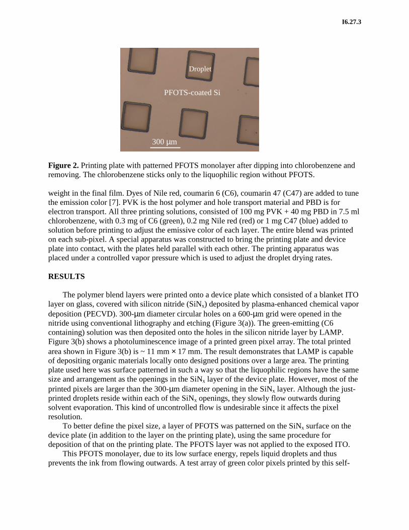
Figure 2. Printing plate with patterned PFOTS monolayer after dipping into chlorobenzene and removing. The chlorobenzene sticks only to the liquophilic region without PFOTS. weight in the final film. Dyes of Nile red, coumarin 6 (C6), coumarin 47 (C47) are added to tune the emission color [7]. PVK is the host polymer and hole transport material and PBD is for electron transport. All three printing solutions, consisted of 100 mg PVK + 40 mg PBD in 7.5 ml chlorobenzene, with 0.3 mg of C6 (green), 0.2 mg Nile red (red) or 1 mg C47 (blue) added to solution before printing to adjust the emissive color of each layer. The entire blend was printed on each sub-pixel. A special apparatus was constructed to bring the printing plate and device plate into contact, with the plates held parallel with each other. The printing apparatus was placed under a controlled vapor pressure which is used to adjust the droplet drying rates. RESULTS
The polymer blend layers were printed onto a device plate which consisted of a blanket ITO layer on glass, covered with silicon nitride (SiNx) deposited by plasma-enhanced chemical vapor deposition (PECVD). 300-µm diameter circular holes on a 600-µm grid were opened in the nitride using conventional lithography and etching (Figure 3(a)). The green-emitting (C6 containing) solution was then deposited onto the holes in the silicon nitride layer by LAMP. Figure 3(b) shows a photoluminescence image of a printed green pixel array. The total printed area shown in Figure 3(b) is ~ 11 mm × 17 mm. The result demonstrates that LAMP is capable of depositing organic materials locally onto designed positions over a large area. The printing plate used here was surface patterned in such a way so that the liquophilic regions have the same size and arrangement as the openings in the SiNx layer of the device plate. However, most of the printed pixels are larger than the 300-µm diameter opening in the SiNx layer. Although the just-printed droplets reside within each of the SiNx openings, they slowly flow outwards during solvent evaporation. This kind of uncontrolled flow is undesirable since it affects the pixel resolution.
To better define the pixel size, a layer of PFOTS was patterned on the SiNx surface on the device plate (in addition to the layer on the printing plate), using the same procedure for deposition of that on the printing plate. The PFOTS layer was not applied to the exposed ITO.
This PFOTS monolayer, due to its low surface energy, repels liquid droplets and thus prevents the ink from flowing outwards. A test array of green color pixels printed by this self-
PFOTS-coated Si
Droplet
300 µm
I6.27.3

Figure 3. (a) Schematic and (b) photoluminescence image of printed layer of PVK/PBD/C6, with a printing plate of 300-µm diameter circles on a 600 µm pitch, onto a device plate of patterned silicon nitride (300-µm circles) on ITO. The wetting of the solvent on to the SiNx leads to poorly-defined feature sizes.
Figure 4. (a) Schematic and (b) photoluminescence image of printed organic layer as in Figure 3, except nitride layer on device plate was coated with PFOTS before printing. Note the improved definition of features. alignment strategy is shown in Figure 4(b). The printed pixels are now uniform in size. An additional benefit of this strategy is that it accommodates any small misalignment during the printing process: even when the printed droplets are slightly misplaced, the PFOTS monolayer will guide them into the predefined location. Similar approaches have been used to improve the location of ink-jet printed drops [2, 8].
To further test the ability of LAMP, we prepared R, G, B full-color pixel arrays by printing. The printing procedure was repeated three times, with the three solutions described earlier, each for a different sub-pixel. A photoluminescence image of a printed RGB pixel array is shown in Figure 5. The pixel size and the spacing between two neighboring pixels are still 300 µm and 600 µm, respectively, with a total printed area of about 20 mm × 20 mm. While we succeeded in
(a)
SiNx
Glass
Printed organics
ITO
PFOTS
SiNx Printed organics
Glass
ITO
(a) (b)
~11 mm
~9 mm
(b)
I6.27.4

Figure 5. A photoluminescence image of printed R, G, B pixel arrays. On the printing plate pixels are circular with a diameter of 300 µm and a pixel to pixel pitch of is 600 µm. Here the total printed area is about 20 × 20 mm2. printing three different patterned films, further work is needed to achieve the uniformity over three successive printing steps.
The electroluminescence of devices made by LAMP is also investigated. OLEDs used for electroluminescence tests are based on the structure shown in Figure 4 with printed green pixels followed by an evaporated Mg:Ag (10:1) layer (50 nm) and a pure Ag layer (100 nm) as the cathode. A shadow mask was used during the cathode evaporation so that each cathode covers about six of the circular devices. Figure 6 shows the I-V characteristics and the photocurrent detected from light emitted by the OLED. For comparison, devices with the same structure, with organic materials deposited by spin coating rather than printing, were also tested. While the printed devices were well behaved, the quantum efficiency was ~ 15% of spin-coated devices. This is thought to be due to the thickness non-uniformity of the organic layer deposited by LAMP, in contrast to a uniform organic layer in the case of spin-coating (90 nm). To achieve comparable quantum efficiency for printed devices, the process should be optimized so that a more thickness-uniform layer is deposited. SUMMARY
In conclusion, we demonstrated a Large-Area wet Micro-Printing (LAMP) technique for organic device patterning. Both single-color and RGB full-color organic pixel arrays of size ~ 20 × 20 mm2 have been patterned by this method. OLEDs in which the organic layer is deposited by this approach have been successfully fabricated. This method could clearly be used to pattern organics for other devices, such as organic thin film transistors. The results given in this work suggest that LAMP is a promising patterning technique for various low-cost organic devices that require the patterning of organic materials.
~20 mm
I6.27.5

Figure 6. Forward current (IF) and detected photocurrent from OLED emission (IPH) vs. forward bias (VF) for spin coated and printed devices. The devices contain about six 300-µm diameter active circles. ACKNOWLEDGEMENTS
This work is supported by the New Jersey Commission on Science and Technology. REFERENCES 1. T.R. Hebner, C.C. Wu, D. Marcy, M.H. Lu, and J.C. Sturm, Appl. Phys. Lett., 72, 519-521
(1998). 2. T. Shimoda, K. Morii, S. Seki, and H. Kiguchi, MRS Bull., 28, 821-827 (2003). 3. A.A. Darhuber, S.M. Troian, and S. Wagner, J. Appl. Phys., 90, 3602-3609 (2001). 4. S.M. Miller, S.M. Troian, and S. Wagner, J. Vac. Sci. Technol., B20, 2320-2327 (2002). 5. A.A. Darhuber, J.P. Valentino, S.M. Troian, and S. Wagner, J. Microelectromech. Syst., 12,
873-879, (2003). 6. J.B. Brzoska, L. Benazouz, and F. Rondelez, Langmuir, 10, 4367-4373, (1994). 7. C.C. Wu, J.C. Sturm, R.A. Register, J. Tian, E.P. Dona, and M.E. Thompson, IEEE Trans.
Elec. Dev. 44, 1269-1281 (1997). 8. H. Sirringhaus, T. Kawase, R.H. Friend, T. Shimoda, M. Inbasekaran, W. Wu, and E. P. Woo,
Science, 290, 2123-2126 (2000).
I6.27.6