Embed Size (px)
Citation preview
GALILEO, University System of GeorgiaGALILEO Open Learning Materials
Engineering Open Textbooks Engineering
Summer 2019
Laboratory Manual for Engineering ElectronicsSandip DasKennesaw State University, [email protected]
Walter ThainKennesaw State University, [email protected]
Sheila HillKennesaw State University, [email protected]
Follow this and additional works at: https://oer.galileo.usg.edu/engineering-textbooksPart of the Electrical and Computer Engineering Commons
This Open Textbook is brought to you for free and open access by the Engineering at GALILEO Open Learning Materials. It has been accepted forinclusion in Engineering Open Textbooks by an authorized administrator of GALILEO Open Learning Materials. For more information, please [email protected].
Recommended CitationDas, Sandip; Thain, Walter; and Hill, Sheila, "Laboratory Manual for Engineering Electronics" (2019). Engineering Open Textbooks. 2.https://oer.galileo.usg.edu/engineering-textbooks/2

Laboratory Manual for Engineering Electronics
Open Textbook Kennesaw State University
Sandip Das, Walter Thain, and Sheila Hill
UNIVERSITY SYSTEMOF GEORGIA

Table of Contents
1. Using LTSpice
2. Instrumentation
3. Operational Amplifiers
4. Differentiator, Integrator, & PWM
5. Diode Characteristics
6. Rectifiers & Regulator
7. MOSFET Behavior
8. CMOS Inverter & Amplifier
9. BJT DC Characteristics
10. BJT Amplifiers

Using LTspice
EE 3401 Laboratory Exercise
Electrical Engineering Department
Kennesaw State University
1 Rev. 5
Objectives:
Students will learn how to use the LTspice circuit simulator, including schematic entry, selecting and
running different simulation types, and how to produce simulation output for reports. Example circuits
will be simulated to demonstrate the capabilities of LTspice.
Introduction:
LTspice is a fully-functional, freely-available circuit simulator. Linear Technology, Inc. originally
designed it so engineers could simulate their switching power supply controller integrated circuits. It is
an excellent SPICE simulator, rivaling costly commercial products like Electronic Workbench and
PSpice. Some important advantages to LTspice are that it is free, circuit sizes are unlimited, it is very
easy to add new models, and the user can easily modify the simulator’s behavior. However, PSpice and
Electronic Workbench have other advantages and are better at mixed analog/digital circuits than
LTspice.
In this lab exercise you will:
• Examine the documentation
• Adjust the schematic window’s user interface with control panel options
• Enter a simple schematic
• Explore the LTspice component library
• Run simulations for
o dc operating point
o ac small-signal frequency response
o time-domain
• Format and create schematic and plot outputs for reports
Equipment:
Computer with LTspice installed.
Procedure:
Starting LTspice
1. Start LTspice by left clicking on the icon . When it starts up, LTspice may ask if you would like to
download an update. Do not do that now.
The screen should look like Fig. 1 if you have a MS Windows PC.
Note: Mac OS users do not have the toolbar under the menu bar.
Note: For both Windows and MAC OS users by right-clicking on the main window and using that
context-based menu.
These instructions will use the context-based menu rather than the toolbar.

2 Rev. 5
Examine the Documentation
A quick overview of the help documentation follows. It serves as the manual but there are some other
online resources and a user’s group that can help with more advanced topics.
2. On the menu bar, left click Help > Help Topics and expand the LTspice XVII heading.
Mac Users: Help > LTspice Help can be found on the File/Edit/Window/Help menu at the top of
the screen.
a. Expand the Schematic Capture topic.
• Left click the first four subtopics so you can see what is covered.
b. Expand the Waveform Viewer topic. This is the waveform plotting utility. Examine Data Trace
Selection, Waveform Arithmetic, Axis Control, and Attached Cursors.
c. Expand the LTspice topic (Mac Users: LTspice Simulator topic). This is where you find the
detailed settings for simulations and the definitions of the circuit elements.
• Expand Dot Commands (Mac Users: Simulator Directives). These are used to set simulation
parameters and select the simulation types.
o In most cases you choose basic simulation settings graphically using the menu or toolbar.
o However, special commands are implemented by placing command text on the schematic
itself. An example of using a dot command is adding a special model you want to use for
one of your circuit elements.
• Expand Circuit Elements. These are the basic circuit element building blocks used in circuits
and subcircuits. The element options are explained in these subtopics.
Fig. 1. MS Windows version startup window with expanded menu and toolbar insert.
3 Rev. 5
d. Expand the Control Panel topic. These functions control simulator program operation, aspects of
the user interface, color schemes for schematics and plots, and plotting parameters.
e. Close the Help window.
Adjust the Schematic Window User Interface
After opening a new schematic, you will make some useful adjustments to the default schematic
graphical user interface settings. There are many other adjustments that you can make to suit your
preference.
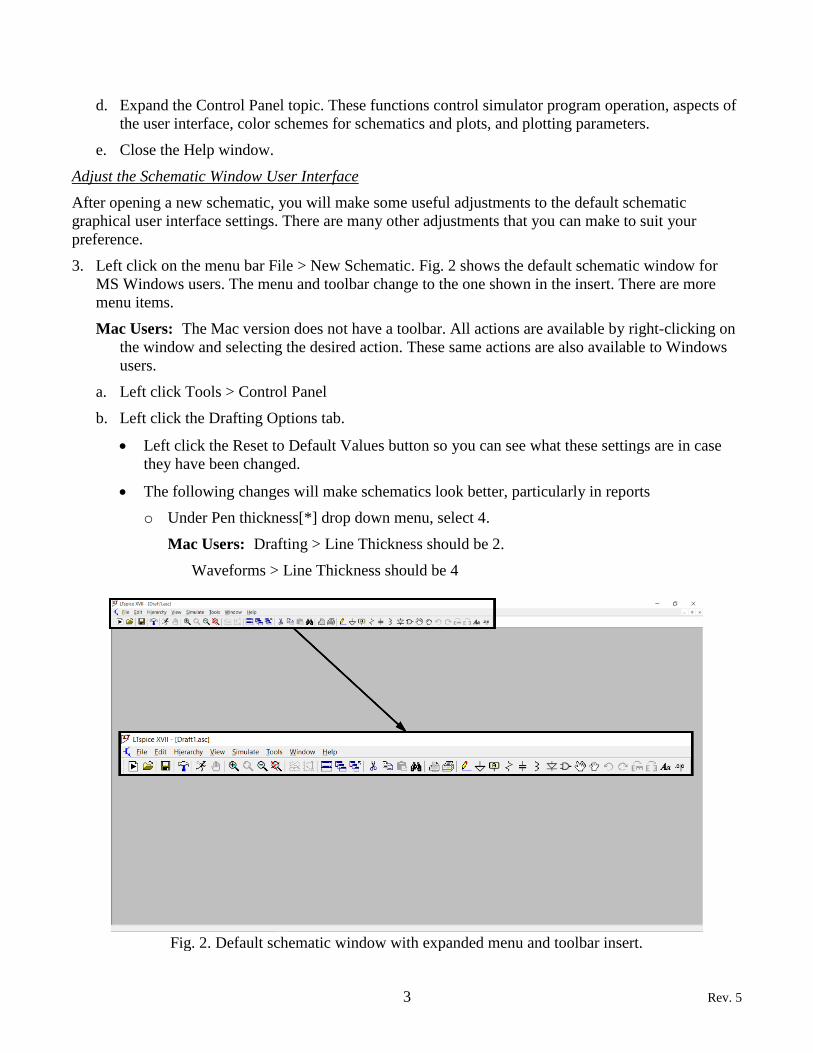
3. Left click on the menu bar File > New Schematic. Fig. 2 shows the default schematic window for
MS Windows users. The menu and toolbar change to the one shown in the insert. There are more
menu items.
Mac Users: The Mac version does not have a toolbar. All actions are available by right-clicking on
the window and selecting the desired action. These same actions are also available to Windows
users.
a. Left click Tools > Control Panel
b. Left click the Drafting Options tab.
• Left click the Reset to Default Values button so you can see what these settings are in case
they have been changed.
• The following changes will make schematics look better, particularly in reports
o Under Pen thickness[*] drop down menu, select 4.
Mac Users: Drafting > Line Thickness should be 2.
Waveforms > Line Thickness should be 4
Fig. 2. Default schematic window with expanded menu and toolbar insert.

4 Rev. 5
o The grey schematic background does not look good in reports if you copy the schematic
to the clipboard, so change it to white as follows.
Left click Color Schemes[*] (Mac Users: Configure Colors).
In the Selected Item box, use the drop-down arrow to select Background.
Move the three RGB sliders all the way to the right so they are at 255.
Left click OK.
• Other settings you can change in the Drafting Options are:
o You may want to change the font properties (type, size, or bold).
Mac Users: There is no way to change font properties such as type, bold, italics, etc.
Size can be changed by right-clicking an individual component name or value.
o You may also want to select Show Schematic Grid Points while you are drawing a
schematic, but these will show up in the schematic if you copy it to the clipboard.
Mac Users: Schematic Grid Points are toggled on or off using the View menu after
right-clicking the schematic to reveal the menu
c. Close the Control Panel.
Enter a Schematic
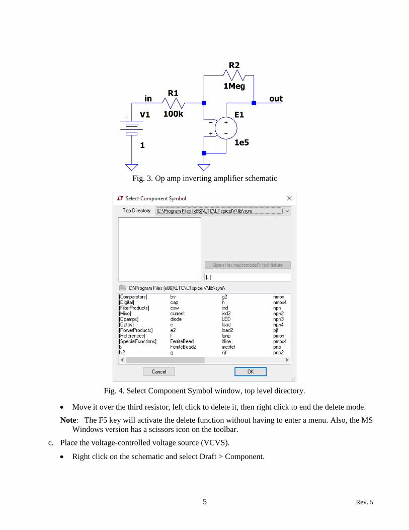
You will construct the circuit in Fig. 3 or one chosen by your instructor. The circuit is a simple model of
an op amp inverting amplifier using standard SPICE elements.
4. Add components to the schematic as follows.
Note: For MS Windows users resistors, capacitors, inductors, diodes, and ground elements have
their own toolbar buttons. All other elements and models are accessed through the component
library button (looks like an AND gate).
a. Place the resistors.
• Right click on the schematic and select Draft > Component. The Select Component Symbol
window will appear as shown in Fig. 4. This directory level has all the standard LTspice
elements. Select res followed by OK. A resistor will attach to the cursor.
• Drag the resistor on the schematic and left click to place it. It doesn’t matter where it is
placed or how it is oriented since it will be moved later.
• Move the mouse and left click to place the second resistor.
• Place a third resistor. You will delete it shortly.
• Right click to end the resistor placement (or press the ESC key).
Note: The F2 key will activate the select component function without having to enter a menu.
b. Deleting a component.
• Right click on the schematic (not the resistor itself) and select Edit > Delete.
• The cursor will change to a scissor icon.
5 Rev. 5
• Move it over the third resistor, left click to delete it, then right click to end the delete mode.
Note: The F5 key will activate the delete function without having to enter a menu. Also, the MS
Windows version has a scissors icon on the toolbar.
c. Place the voltage-controlled voltage source (VCVS).
• Right click on the schematic and select Draft > Component.
Fig. 3. Op amp inverting amplifier schematic
Fig. 4. Select Component Symbol window, top level directory.

6 Rev. 5
• VCVS elements are identified by the letter “e” in all versions of SPICE. LTspice has two
symbols, “e” and “e2”.
o First click on the e and the symbol will appear in the top left box of the Select
Component Symbol window.
o Then click on the e2 and that symbol will appear. Note the difference is just the
orientation of the + and – signs on the VCVS input leads.
o The circuit in Fig. 3 uses e2, so left click on that one and then click OK.
o Place it on the schematic as you did with the resistor. It will be moved later.
o Right click to end the VCVS placement (or press the ESC key).
d. Place the independent voltage source.
• Right click on the schematic and select Draft > Component.
• Navigate to the “voltage” element in the top-level directory and left click on it.
o Its symbol is a standard independent voltage source and not one that looks like a battery
as in the schematic. However, it can be used for a dc source too.
o You will use a battery symbol and not this one, but the standard voltage source symbol is
more popular.
• Locate and double left click on the [Misc] directory link.
o Select the “battery” symbol and then left click OK.
o Place it on the schematic and then right click when you are done.
e. Place the ground (0-volt node) reference symbol.
• Right click on the schematic and select Draft > Label Net.
• Select GND (global node 0), then OK. Place the GND symbol on the schematic.
• You can place more than one ground symbol on a schematic, which can make the wiring
neater.
• Right click when you are done placing grounds.
Note: The MS Windows version has a ground icon on the toolbar.
5. Arrange components and connect them with wires as follows.
a. To move and rotate components, use the Move tool (looks like a hand with open fingers).
• Right click on the schematic and select Edit > Move. Or you can use F7.
• Click on one of the two resistors.
• While the resistor is “active”, press Ctrl-R to rotate it to horizontal and move it to its final
position. Then left click to place it.
• Repeat the process to place the second resistor.
• Move the voltage sources to their final positions.

7 Rev. 5
b. Wire the schematic using the wire tool (looks like a pencil).
• Right click on the schematic and select Draft > Draw Wire. Or you can use F3.
• Move the mouse position to one of the element leads using the crosshairs to find it.
• Left click to start the wire. You do not have to hold the mouse button down.
• Drag the wire to the next element. You can make bends by left clicking and changing the
wire direction.
• When you reach the next element, left click on its lead and the wire will terminate.
Note: If you want to finish a wire open-ended and not on an element, left click, then right click
where you want to end it.
c. More on moving components.
• The Move tool will move components and individual wire segments when you left click on
them.
• You can move a group of components by first drawing a select box with the Move tool hand.
o Position the Move hand where you want to start the select box. Click and hold the left
button and drag it to select the components you want. Then release the left button.
o Then drag the selected components where you want them to go.
d. Dragging components.
• The Drag tool is the hand symbol that looks like a fist .
• Dragging leaves wires connected and can be more convenient at times.
6. Elements are automatically given reference designator labels as they are placed on the schematic.
LTspice uses them as unique identifiers. Elements usually do not have default values, but if they do,
they usually need to be changed. Fig. 5 shows circuit element labels and values.
a. Changing resistor values and designator labels is done as follows.
• You can change the designator label by right clicking on it and entering text. You do not
need to change it for this exercise, but resistor designator labels must start with the letter R.
Fig. 5. Element designator labels and values.

8 Rev. 5
• The initial value for all resistors is the placeholder letter R. It does not represent a numerical
value.
o Right click on the R and change the value to what you want.
o Numbers like 1e5 or 1E5 are equivalent to 100k, 100000, and 0.1Meg.
Note: Exponential notation follows the syntax above. Characters like “10” and “^” are
meaningless and can cause errors. See Table 1.
b. Changing the independent voltage source value and designator label is done as follows.
• The designator is changed the same way as with resistors. You do not need to change it for
this exercise, but independent voltage source designator labels must start with the letter V.
• To change the value, right click on the placeholder letter V. Enter the dc voltage you want.
• You can also change the value by right-clicking on the voltage source element, which opens
the Voltage Source dialog box.
o Enter the dc value you want in the box.
o Note that if you left click the Advanced button, you can give the source values for other
simulation types.
“Functions” waveform types are for Transient (time-domain) simulations.
“DC Value” is for operating point and transient simulations.
“Small signal AC” is for ac analysis (frequency sweep) simulations.
c. Changing the VCVS scale factor and designator label is done as follows.
• The designator is changed the same way as with resistors. You do not need to change it for
this exercise, but VCVS designator labels must start with the letter E.
• To change the scale factor, right click on the placeholder letter E. Enter the scale factor you
want.
o The scale factor does not have to be a constant value
Table 1: SPICE number notation.
Suffix Multiplier
T 1e12
G 1e9
Meg 1e6
K 1e3
mil 25.4e-6
m 1e-3
u(or μ) 1e-6
n 1e-9
p 1e-12
f 1e-15

9 Rev. 5
o It can be an equation involving other circuit parameters. See the Help section on Voltage
Dependent Voltage Source.
• You can also change the scale factor by right-clicking on the element which opens the
Component Attributes Editor box.
o Change the scale factor in the Value row, Value column.
d. Labeling circuit nodes makes it easier to find them in the simulation results.
• Label the input node between V1 and R1 as follows.
o Right click on the wire, then left click Label Net.
o The Net Name dialog box will appear. Type “in” (without quotes) in the box, then left
click OK.
o A box will attach to the cursor that has a small square anchor point. Position the anchor
point on the wire and left click to anchor it to the wire. Then right click to stop the mode.
o You can remove net names with the Delete tool.
• Label the output node “out”.
e. Save your circuit schematic by first left clicking File > Save As. Navigate to a desired folder or
create a new one and enter a filename. Then click Save.
Note: You should save files frequently and use different filenames when appropriate.
Running Simulations and Documenting Results
You will run three simulations, a dc operating point analysis, a time-domain analysis, and a small-signal
frequency response analysis. You will also learn how to plot waveforms, use cursors, and format plots
for reports.
7. DC operating point simulation. The schematic you just entered uses an independent dc voltage
source, so you will perform a dc analysis first.
a. Set up the dc operating point analysis and save results as follows.
• On the menu at the top of the window, left click Simulate > Edit Simulation Command.
Mac Users: Right-click, Draft > Spice Directive
• Left click the DC op pnt tab (Mac Users: Type .op into the empty text box). There are no
parameters to specify, so left click OK.
o A box will attach itself to the cursor.
o Move the cursor to an empty part of the schematic and left click.
o The dot command .op will appear. You can use the Move function to move the .op
command text somewhere else.
b. Run the .op simulation by clicking Simulate > Run (looks like a running person) on the main
menu.
• For MS Windows users, a window with the results will appear.

10 Rev. 5
Mac Users: Operating point simulation results are found in the SPICE Error Log. Right-
click to reveal the menu, then View > SPICE Error Log.
• Reduce the size of the window to include just the output data.
o Put the cursor over the lower right corner, until a double arrow appears.
o Left click, hold and drag the window to an appropriate size.
c. Open a new document in MS Word or a similar word processor, then copy and paste the results
in it as follows.
• Click on the window with the .op simulation results to make it active.
• MS Windows can copy the .op results window to the clipboard by pressing keys Alt-PrtScr at
the same time when that window is active.
Mac Users: Select the relevant text, right-click and copy
• In the document, paste the clipboard bitmap of the .op results window.
• Resize it in the document so the results are readable.
d. Copy the schematic to the document as follows.
• Return to LTspice and copy the schematic to the document as follows.
• Close the .op results window.
• Right click on the schematic window and select View > Zoom to Fit . This will expand the
schematic to maximum size.
• On the menu, left click Tools > Copy bitmap to Clipboard.
Mac Users: Use Screenshot, save the photo, then add the photo to the document.
• Then paste the clipboard bitmap into the document.
• Crop and resize it as needed to make it an appropriate size. This is how the schematic figure
images were generated for these instructions.
8. Time-domain simulation. The next simulation is a time-domain analysis with the independent
voltage source changed to a sine wave. You could use the battery source for this since it is a fully-
functional independent voltage source. However, you will change it to the general voltage source
you saw earlier.
a. Change the voltage source.
• Delete the battery source.
• Open the Select Component Symbol window as done earlier.
Mac Users: Draft > Component > type vo into the search box. The independent voltage
source will be selected.
• Find and select the Voltage independent source and place it on the schematic where the
battery used to be.
b. Adjust the source to be a 1 Vp-p, 1 kHz sine wave as follows.
11 Rev. 5
• Right click on the source and the Voltage Source dialog box will appear.
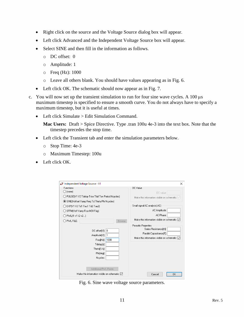
• Left click Advanced and the Independent Voltage Source box will appear.
• Select SINE and then fill in the information as follows.
o DC offset: 0
o Amplitude: 1
o Freq (Hz): 1000
o Leave all others blank. You should have values appearing as in Fig. 6.
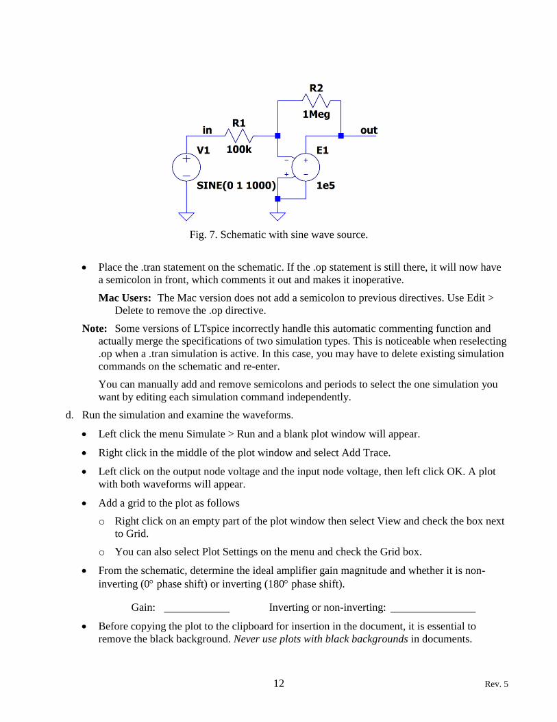
• Left click OK. The schematic should now appear as in Fig. 7.
c. You will now set up the transient simulation to run for four sine wave cycles. A 100 s
maximum timestep is specified to ensure a smooth curve. You do not always have to specify a
maximum timestep, but it is useful at times.
• Left click Simulate > Edit Simulation Command.
Mac Users: Draft > Spice Directive. Type .tran 100u 4e-3 into the text box. Note that the
timestep precedes the stop time.
• Left click the Transient tab and enter the simulation parameters below.
o Stop Time: 4e-3
o Maximum Timestep: 100u
• Left click OK.
Fig. 6. Sine wave voltage source parameters.
12 Rev. 5
• Place the .tran statement on the schematic. If the .op statement is still there, it will now have
a semicolon in front, which comments it out and makes it inoperative.
Mac Users: The Mac version does not add a semicolon to previous directives. Use Edit >
Delete to remove the .op directive.
Note: Some versions of LTspice incorrectly handle this automatic commenting function and
actually merge the specifications of two simulation types. This is noticeable when reselecting
.op when a .tran simulation is active. In this case, you may have to delete existing simulation
commands on the schematic and re-enter.
You can manually add and remove semicolons and periods to select the one simulation you
want by editing each simulation command independently.
d. Run the simulation and examine the waveforms.
• Left click the menu Simulate > Run and a blank plot window will appear.
• Right click in the middle of the plot window and select Add Trace.
• Left click on the output node voltage and the input node voltage, then left click OK. A plot
with both waveforms will appear.
• Add a grid to the plot as follows
o Right click on an empty part of the plot window then select View and check the box next
to Grid.
o You can also select Plot Settings on the menu and check the Grid box.
• From the schematic, determine the ideal amplifier gain magnitude and whether it is non-
inverting (0 phase shift) or inverting (180 phase shift).
Gain: Inverting or non-inverting:
• Before copying the plot to the clipboard for insertion in the document, it is essential to
remove the black background. Never use plots with black backgrounds in documents.
Fig. 7. Schematic with sine wave source.

13 Rev. 5
o On the menu bar, left click Tools > Color Preferences.
Left click the Waveform tab.
In the Select Item box, choose Background.
Move the three sliders all the way right so the numbers in the boxes are 255.
Left click OK and you will return to the plot.
o The axes are grey and a better choice for a white background is black.
Return to the Color Preferences box.
Select Axis and move the sliders all the way to the left so the numbers in the boxes
are 0.
Click Apply.
Now select Grid and make it black.
o The trace colors that look good with a black background may not with a white
background, particularly light green. You will change this trace to the same color as
V[11] but you need to see what its color numbers are first.
Select Trace V[11] and note the color numbers.
Select Trace V[1] and change the color numbers to the ones you just found.
Left click OK.
• The trace font size should be made larger than the default value.
o On the menu bar, left click Tools > Control Panel.
o Click on Reset to Default Values to see what those settings are.
o Under Pen thickness[*] drop down menu, select 4.
o Change the Font to Arial with 20-point size and select Bold font.
Mac Users: This step cannot be done on the Mac version.
o Left click OK.
o The plot should look like the one in Fig. 8.
e. Adjust the plot axis scaling and copy it to the document.
• Adjust the time axis as follows.
o Move the mouse over the horizontal axis until it displays a small ruler.
o Right click and the Horizontal Axis dialog box appears.
o Replace 4 ms with 2 ms.
o Click OK.
• Copy the plot to the clipboard.
o On the menu, left click Tools > Copy bitmap to Clipboard.
14 Rev. 5
Mac Users: Use the Screenshot function.
o Paste the plot in the document.
o Resize the plot so it is 5.5-inch wide.
f. Copy the schematic to the clipboard and then to the document as before.
9. AC analysis simulation. The last simulation is an ac analysis frequency sweep with the independent
voltage source changed to an ac version with 1 V amplitude. The circuit is changed to be a single-
pole lowpass filter with a 10 kHz cutoff frequency. You will make a Bode plot to display the
amplifier gain vs. signal frequency, and using cursors, find the 3 dB frequency where the gain
magnitude is 3 dB lower than the maximum at 0 Hz.
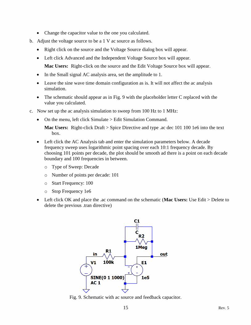
a. Convert the amplifier to a single-pole lowpass filter as follows.
• Left click on the Capacitor button on the toolbar and place a capacitor just above the 1 M
feedback resistor. Rotate it to be horizontal.
Mac Users: Right-click Draft > Component and type c in the search box to select the
capacitor. Click OK and hit Ctrl-R to rotate before placing on the schematic.
• Connect the capacitor in parallel with the feedback resistor.
• Calculate the value needed to set the cutoff frequency to fc = 10 kHz where the response will
be down 3 dB. Eq. 1 shows the relationship between the cutoff frequency, R2, and C values.
2
1
2 c
CR f
= (1)
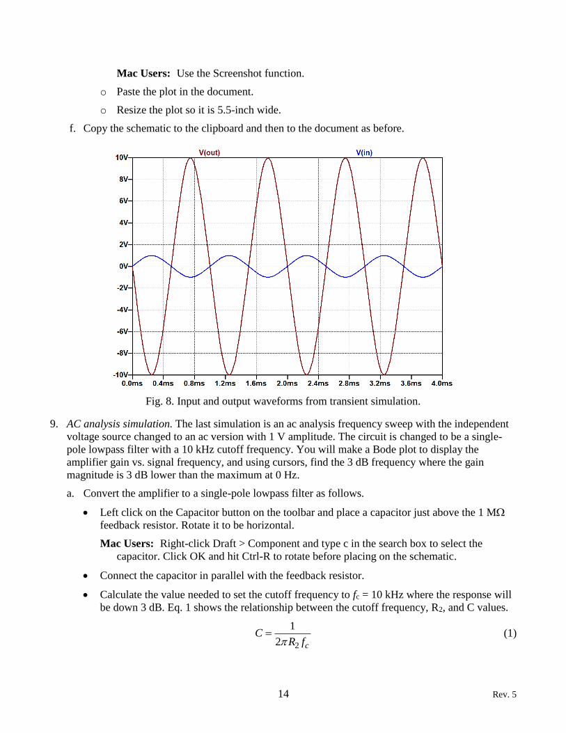
Fig. 8. Input and output waveforms from transient simulation.
15 Rev. 5
• Change the capacitor value to the one you calculated.
b. Adjust the voltage source to be a 1 V ac source as follows.
• Right click on the source and the Voltage Source dialog box will appear.
• Left click Advanced and the Independent Voltage Source box will appear.
Mac Users: Right-click on the source and the Edit Voltage Source box will appear.
• In the Small signal AC analysis area, set the amplitude to 1.
• Leave the sine wave time domain configuration as is. It will not affect the ac analysis
simulation.
• The schematic should appear as in Fig. 9 with the placeholder letter C replaced with the
value you calculated.
c. Now set up the ac analysis simulation to sweep from 100 Hz to 1 MHz:
• On the menu, left click Simulate > Edit Simulation Command.
Mac Users: Right-click Draft > Spice Directive and type .ac dec 101 100 1e6 into the text
box.
• Left click the AC Analysis tab and enter the simulation parameters below. A decade
frequency sweep uses logarithmic point spacing over each 10:1 frequency decade. By
choosing 101 points per decade, the plot should be smooth ad there is a point on each decade
boundary and 100 frequencies in between.
o Type of Sweep: Decade
o Number of points per decade: 101
o Start Frequency: 100
o Stop Frequency 1e6
• Left click OK and place the .ac command on the schematic (Mac Users: Use Edit > Delete to
delete the previous .tran directive)
Fig. 9. Schematic with ac source and feedback capacitor.
16 Rev. 5
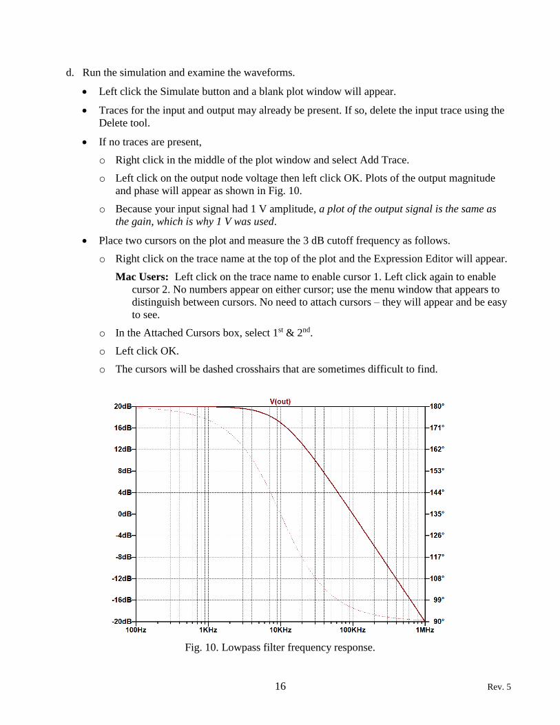
d. Run the simulation and examine the waveforms.
• Left click the Simulate button and a blank plot window will appear.
• Traces for the input and output may already be present. If so, delete the input trace using the
Delete tool.
• If no traces are present,
o Right click in the middle of the plot window and select Add Trace.
o Left click on the output node voltage then left click OK. Plots of the output magnitude
and phase will appear as shown in Fig. 10.
o Because your input signal had 1 V amplitude, a plot of the output signal is the same as
the gain, which is why 1 V was used.
• Place two cursors on the plot and measure the 3 dB cutoff frequency as follows.
o Right click on the trace name at the top of the plot and the Expression Editor will appear.
Mac Users: Left click on the trace name to enable cursor 1. Left click again to enable
cursor 2. No numbers appear on either cursor; use the menu window that appears to
distinguish between cursors. No need to attach cursors – they will appear and be easy
to see.
o In the Attached Cursors box, select 1st & 2nd.
o Left click OK.
o The cursors will be dashed crosshairs that are sometimes difficult to find.
Fig. 10. Lowpass filter frequency response.

17 Rev. 5
o Move the mouse around the plot until a yellow “1” appears.
o Left click and hold and drag the cursor all the way down to 100 Hz.
o Note the cursor 1 magnitude.
This is the gain magnitude at 100 Hz and is very close to the maximum gain that
occurs at 0 Hz.
Gain at 100 Hz in dB:
Convert the gain in dB to a non-dB gain magnitude.
Gain at 100 Hz (non-dB):
Is this expected value?
o Move the mouse around the plot until a yellow “2” appears.
o Left click and hold and drag the cursor until the Ratio (Cursor2/Cursor1) magnitude is
−3.00 0.02 dB.
o Read the cursor 2 frequency. Determine the percent error between 10 kHz and the cursor
2 frequency.
Cutoff frequency:
o Place a marker at the 3 dB point as follows.
On the plot menu, select Plot Settings > Notes and Annotations > Label Curs. Pos.
Mac Users: Use Draw > Text to create a text label (this can’t be edited so type carefully.
Use Draw > Arrow to make an arrow from the label to the point on the trace.
You can right click on the label text and change or delete it.
You can also delete the label and arrow using the Delete tool.
e. Copy the plot and paste it in the document.
• Left click Tools > Copy bitmap to Clipboard (Mac Users: Use Screenshot)
• Paste the plot in the document.
• Resize the plot so it is 5.5-inch wide.
Results Documentation Summary
10. You should have the following documentation from the procedure steps.
a. You should have three schematics, one from each simulation.
b. You should have an image of the dc simulation results and one plot from the transient simulation
and one from the ac simulation.
c. Be sure that you recorded data and calculated results in steps you were asked to.
d. Check with your instructor for additional documentation requirements.

Instrumentation
EE 3401 Laboratory Exercise
Electrical Engineering Department
Kennesaw State University
1 Rev. 5
Objectives:
Students will learn how to make measurements using a function generator and oscilloscope. The basic
features of both instruments are examined. Also, methods for improving displayed waveform quality are
explored.
Introduction:
The typical equipment you find in an electronics laboratory are a DC power supply, a multimeter, a
function generator, and an oscilloscope. In this exercise, you will use some of the most popular features
of the function generator and oscilloscope to make measurements. You will build a voltage divider with
a low voltage output and use features of the oscilloscope to improve the displayed waveform.
Equipment:
Agilent (Keysight) 33220A Function/Arbitrary Waveform Generator
Agilent (Keysight) DSO 5014A Oscilloscope
Cables and oscilloscope probes as needed
Solderless breadboard and required components – see instructions
Components:
Resistors (Qty): 1 k (1), 1 M (1)
Procedure:
Function Generator
You will start with the function generator. The Agilent 33220A Function/Arbitrary Waveform Generator
(abbreviated FG or AWG) produces the usual function generator waveforms (sine, square, triangle, etc.)
plus arbitrary waveform shapes downloaded into its memory. The most important AWG specifications
are given in the appendix, Table 1.
1. Set up the AWG for a 1 kHz, 1 Vpeak-peak sine wave as follows.
a. First you need to change the generator’s configuration so that the output amplitude value you see
on the display will be more accurate for the typical load impedances you connect it to.
By default, the function generator expects to be connected to a 50 Ω load. Since it also has a 50
Ω output impedance, this forms a voltage divider at the output connector with a ratio of ½. The
equivalent circuit is in Fig. 1. The generator takes this assumption into account, so if you set the
output to 1 Vp-p, the AWG sets Vgen to 2 Vp-p so that Vout = 1 Vpp.
When you connect a high load impedance like 10 kΩ, the divider ratio is actually 10,000/10,050
= 0.995 and Vout = 1.99 Vp-p. But, the display will still read 1 Vp-p because of the 50 Ω load
assumption.
The solution is to change the generator’s assumed load impedance to open circuit by putting it in
High-Z mode.
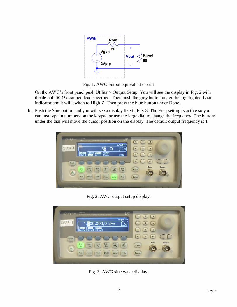
2 Rev. 5
On the AWG’s front panel push Utility > Output Setup. You will see the display in Fig. 2 with
the default 50 Ω assumed load specified. Then push the grey button under the highlighted Load
indicator and it will switch to High-Z. Then press the blue button under Done.
b. Push the Sine button and you will see a display like in Fig. 3. The Freq setting is active so you
can just type in numbers on the keypad or use the large dial to change the frequency. The buttons
under the dial will move the cursor position on the display. The default output frequency is 1
Fig. 2. AWG output setup display.
Fig. 3. AWG sine wave display.
Fig. 1. AWG output equivalent circuit
3 Rev. 5
kHz, which is what you want, so don’t change it.
Note: It’s best to use Freq, Ampl, and Offset settings and not Period, HiLevel and LoLevel
settings.
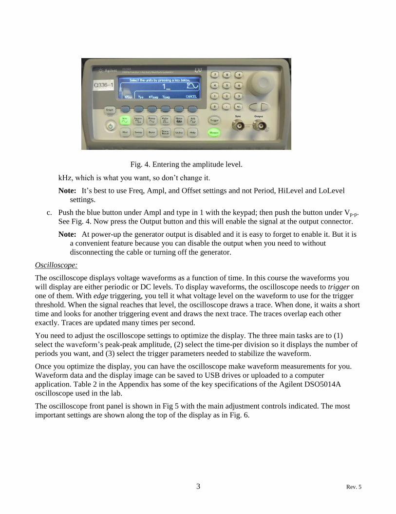
c. Push the blue button under Ampl and type in 1 with the keypad; then push the button under Vp-p.
See Fig. 4. Now press the Output button and this will enable the signal at the output connector.
Note: At power-up the generator output is disabled and it is easy to forget to enable it. But it is
a convenient feature because you can disable the output when you need to without
disconnecting the cable or turning off the generator.
Oscilloscope:
The oscilloscope displays voltage waveforms as a function of time. In this course the waveforms you
will display are either periodic or DC levels. To display waveforms, the oscilloscope needs to trigger on
one of them. With edge triggering, you tell it what voltage level on the waveform to use for the trigger
threshold. When the signal reaches that level, the oscilloscope draws a trace. When done, it waits a short
time and looks for another triggering event and draws the next trace. The traces overlap each other
exactly. Traces are updated many times per second.
You need to adjust the oscilloscope settings to optimize the display. The three main tasks are to (1)
select the waveform’s peak-peak amplitude, (2) select the time-per division so it displays the number of
periods you want, and (3) select the trigger parameters needed to stabilize the waveform.
Once you optimize the display, you can have the oscilloscope make waveform measurements for you.
Waveform data and the display image can be saved to USB drives or uploaded to a computer
application. Table 2 in the Appendix has some of the key specifications of the Agilent DSO5014A
oscilloscope used in the lab.
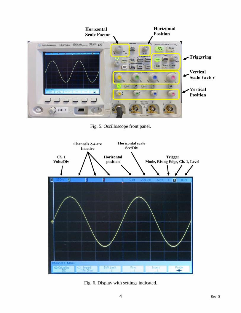
The oscilloscope front panel is shown in Fig 5 with the main adjustment controls indicated. The most
important settings are shown along the top of the display as in Fig. 6.
Fig. 4. Entering the amplitude level.
4 Rev. 5
Fig. 5. Oscilloscope front panel.
Fig. 6. Display with settings indicated.
Ch. 1
Volts/Div
Channels 2-4 are
Inactive
Horizontal
position
Horizontal scale
Sec/Div
Trigger
Mode, Rising Edge, Ch. 1, Level

5 Rev. 5
2. You will set up the oscilloscope to display the AWG waveform on Channel 1.
When you choose the oscilloscope vertical, horizontal, and trigger settings, you need to have some
idea of what the waveform should look like. Three guidelines are: (don’t do these on the
oscilloscope yet).
Choose a vertical scale so that the waveform occupies 3 to 6 divisions.
Choose a horizontal scale so that 2 to 4 periods are displayed.
Choose edge triggering. Select rising or falling edge. Select auto trigger mode. Select a
trigger voltage in the middle of the waveform’s voltage swing (approximately the
waveform’s average voltage).
Once you have a stable display you can readjust it as desired.
Note: The normal, or Norm trigger mode will not display a trace at all if a trigger event is not
detected, so it can be hard to set up the display in this mode. The automatic or Auto mode will
always display a trace but if a trigger event is not detected the trace will be unstable.
a. Connect the AWG output (not the sync) to the oscilloscope Ch. 1 input with a cable. The
waveform may not look like the one in Fig. 6 at this time.
b. The AWG output should be a 1 Vp-p, 1 kHz sine wave, so calculate appropriate settings:
Calculate the vertical scale factor so the peak-peak waveform amplitude will span 5 divisions.
Calculated scale factor (volts/div):
Now calculate the waveform period.
Waveform period:
From the calculated period, determine the horizontal scale factor that results in 2 periods across
the 10 horizontal divisions.
Horizontal scale factor (sec/div):
Calculate the voltage that is midway between the waveform positive and negative peaks:
Midpoint voltage:
c. Now adjust the settings as in the procedure below. The displayed waveform may not be stable
until you complete the settings adjustments.
Press the “1” button in the Ch. 1 vertical control area so it is lit. This activates Ch. 1 (Fig. 7.)
Adjust the Ch. 1 vertical position so the trace ground reference is at the display center. Fig. 8
shows the ground reference level indicator (has a “1” next to it) and the trigger level indicator
(has a “T” next to it) on the left side of the display. The ground level in Fig. 8 is above the
center so you can see it.
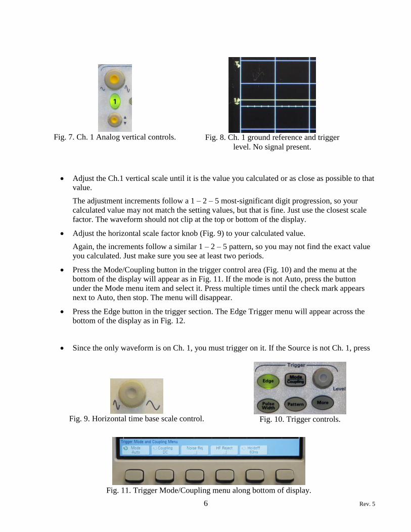
6 Rev. 5
Adjust the Ch.1 vertical scale until it is the value you calculated or as close as possible to that
value.
The adjustment increments follow a 1 – 2 – 5 most-significant digit progression, so your
calculated value may not match the setting values, but that is fine. Just use the closest scale
factor. The waveform should not clip at the top or bottom of the display.
Adjust the horizontal scale factor knob (Fig. 9) to your calculated value.
Again, the increments follow a similar 1 – 2 – 5 pattern, so you may not find the exact value
you calculated. Just make sure you see at least two periods.
Press the Mode/Coupling button in the trigger control area (Fig. 10) and the menu at the
bottom of the display will appear as in Fig. 11. If the mode is not Auto, press the button
under the Mode menu item and select it. Press multiple times until the check mark appears
next to Auto, then stop. The menu will disappear.
Press the Edge button in the trigger section. The Edge Trigger menu will appear across the
bottom of the display as in Fig. 12.
Since the only waveform is on Ch. 1, you must trigger on it. If the Source is not Ch. 1, press
Fig. 9. Horizontal time base scale control.
Fig. 10. Trigger controls.
Fig. 11. Trigger Mode/Coupling menu along bottom of display.
Fig. 8. Ch. 1 ground reference and trigger
level. No signal present.
Fig. 7. Ch. 1 Analog vertical controls.

7 Rev. 5
the button under the Source indicator until the selection menu pops up. Press multiple times
until the check mark appears next to Ch. 1, then stop. The menu will disappear.
Choose the positive-going slope (arrow below Slope points up).
Now adjust the trigger voltage level to the midpoint voltage value you calculated in part 2(b)
by turning the small Level knob in the trigger section. Once this is done, the waveform
should be stable.
Note: If you are on a low V/div scale like 10 mV/div and the trigger level is way off, it can take
many Level knob turns to set the level to what you want. You can speed up the process by
changing the vertical scale to a higher value and then adjusting the trigger level to bring it
close. Then reset the vertical scale to the one you want and fine-tune the trigger.
Have your instructor verify that your display is stable.
d. You can have the oscilloscope automatically scale a waveform and trigger on it by pressing the
Autoscale button (Fig. 13.).
While this is convenient, you should not have to resort to this method just to display a waveform.
Note: Autoscale can produce unexpected results. For example, the oscilloscope may trigger on
a high-frequency noise signal. You can tell if this happened when your waveform does not
look right. When looking at the amplitude and horizontal scale settings you will likely see a
very small vertical scale and a very small time/div (usually nanoseconds/div).
Press the Autoscale button and see what happens.
3. Making automatic measurements.
The oscilloscope can display up to four simultaneous automatic. It’s easier than using time and
voltage cursors to make the measurements manually. The measurements can be made on any
waveform and between waveforms. The most popular ones are peak-peak amplitude, average level
(same as DC level), frequency, period, and phase difference.
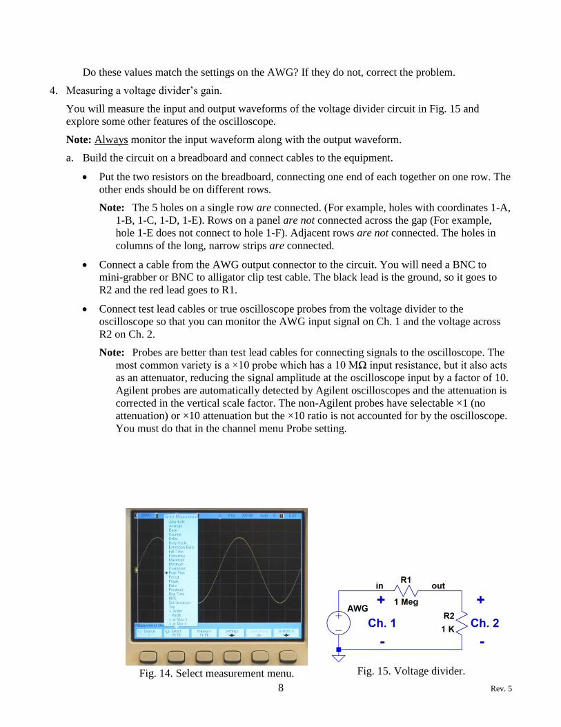
a. Press the Quick Meas button shown in Fig. 13 and the Measurement Menu will appear. From the
menu, you choose the source channel, the measurement you want, and then display it. When you
press the Select button the menu in Fig. 14 appears. You can keep pressing Select until the arrow
points to the desire measurement, or you can use the Select Knob next to the Autoscale button to
do the same.
b. Have the oscilloscope measure the AWG waveform peak-peak amplitude and frequency. You
will have to select two measurements, one at a time. You may have to clear existing
measurements with the Clear Meas menu.
Frequency: Peak-peak voltage:
Fig. 13. Autoscale and Measure controls.
Fig. 12. Edge Trigger menu along bottom of display.
8 Rev. 5
Do these values match the settings on the AWG? If they do not, correct the problem.
4. Measuring a voltage divider’s gain.
You will measure the input and output waveforms of the voltage divider circuit in Fig. 15 and
explore some other features of the oscilloscope.
Note: Always monitor the input waveform along with the output waveform.
a. Build the circuit on a breadboard and connect cables to the equipment.
Put the two resistors on the breadboard, connecting one end of each together on one row. The
other ends should be on different rows.
Note: The 5 holes on a single row are connected. (For example, holes with coordinates 1-A,
1-B, 1-C, 1-D, 1-E). Rows on a panel are not connected across the gap (For example,
hole 1-E does not connect to hole 1-F). Adjacent rows are not connected. The holes in
columns of the long, narrow strips are connected.
Connect a cable from the AWG output connector to the circuit. You will need a BNC to
mini-grabber or BNC to alligator clip test cable. The black lead is the ground, so it goes to
R2 and the red lead goes to R1.
Connect test lead cables or true oscilloscope probes from the voltage divider to the
oscilloscope so that you can monitor the AWG input signal on Ch. 1 and the voltage across
R2 on Ch. 2.
Note: Probes are better than test lead cables for connecting signals to the oscilloscope. The
most common variety is a ×10 probe which has a 10 MΩ input resistance, but it also acts
as an attenuator, reducing the signal amplitude at the oscilloscope input by a factor of 10.
Agilent probes are automatically detected by Agilent oscilloscopes and the attenuation is
corrected in the vertical scale factor. The non-Agilent probes have selectable ×1 (no
attenuation) or ×10 attenuation but the ×10 ratio is not accounted for by the oscilloscope.
You must do that in the channel menu Probe setting.
Fig. 14. Select measurement menu.
Fig. 15. Voltage divider.
9 Rev. 5
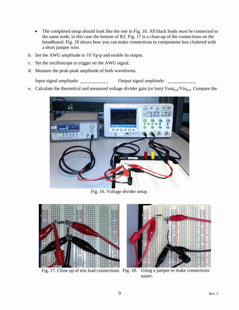
The completed setup should look like the one in Fig. 16. All black leads must be connected to
the same node, in this case the bottom of R2. Fig. 17 is a close-up of the connections on the
breadboard. Fig. 18 shows how you can make connections to components less cluttered with
a short jumper wire.
b. Set the AWG amplitude to 10 Vp-p and enable its output.
c. Set the oscilloscope to trigger on the AWG signal.
d. Measure the peak-peak amplitude of both waveforms.
Input signal amplitude: Output signal amplitude:
e. Calculate the theoretical and measured voltage divider gain (or loss) Voutp-p/Vinp-p. Compare the
Fig. 16. Voltage divider setup.
Fig. 17. Close up of test lead connections.
Fig. 18. Using a jumper to make connections
easier.

10 Rev. 5
two using a percent error calculation as in Eq. 1.
100%M easured Theoretical
Percent errorTheoretical
(1)
Theoretical divider gain: Measured divider gain:
Percent error:
f. Low-level signals like the one on Ch. 2 can have noise on it, which makes the automatic
measured peak-peak voltage value too large.
Go into the Ch. 2 menu and turn on the bandwidth limit (BW Limit). When activated the
small square under BW Limit will be dark.
Remeasure the output signal amplitude and recalculate the measured divider gain.
BW Limit output signal amplitude:
Remeasured divider gain:
Percent error from calculated divider gain:
g. Averaging is the best way to reduce noise on a trace. But, the triggering must be stable for it to
work. High resolution mode (Hi Res) is about as good and does not require stable triggering. In
these two modes, all waveforms are affected, not just one channel.
Turn off BW Limit on Ch. 2.
In the Waveform section, press the Acquire button. Activate the Acq Mode menu and select
Hi Res or Average. Then try the other to see which removes the most noise.
Remeasure the output signal amplitude and recalculate the measured divider gain.
Averaged or Hi Res output signal amplitude:
Remeasured divider gain:
Percent error from calculated divider gain:
Account for the difference between the calculated and measured divider gain.
h. Now turn off waveform averaging or high resolution mode.
5. More on triggering.
The best signal to trigger on is the Sync output of the function generator. After that the next best
signal is the one with the largest amplitude. However, you may find that you must trigger on low-
level, noisy signals. The trigger circuit has low pass filters you can select to help with triggering on
small signals.
a. Change your trigger source to the divider output on Ch. 2 and adjust the trigger level to the
center of the waveform.
b. The waveform may not be stable. If it is, lower the AWG amplitude by 1 Vp-p increments until
the waveform is not stable.

11 Rev. 5
c. Go into the trigger Mode/Coupling menu and try activating high-frequency reject (HF Reject) or
Noise Reject.
Did HF Reject or Noise Reject stabilize the triggering?
6. Saving waveforms.
Saving oscilloscope display images is the best way to document your measurements. If the
oscilloscope is connected to a computer running Keysight (Agilent) BenchVue, it is the most
convenient way to save waveforms.
If not, waveforms can be saved to a USB drive inserted in the front panel connector.
Note: when saving a display image, invert the graticule colors so that the display’s background is
white. It saves toner/ink when printing and looks better on white paper.
a. Insert a USB flash drive in the front panel connector.
Note: The largest capacity USB drive the oscilloscope can read is 4 GB.
b. Press the Save/Recall button in the File section (Fig. 19) and the Save/Recall menu will appear
on the display.
c. Press the button under Save and its menu will appear on the display.
d. In the Save menu, press the button under Format and select either a bitmap (BMP) or portable
network graphics (PNG) image file format. You will automatically return to the Save menu in a
few seconds.
e. In the Save menu, make sure Save To says usb0. You will automatically return to the Save menu
in a few seconds.
f. Changing the file name is optional. If you want to, press the button under File Name and make
the changes. Return to the Save menu by pressing the button under the up arrow .
Note: The oscilloscope will use a default name starting with “scope_0” and will increment the
number automatically each time you save a display image.
g. In the Save menu, press the button under Settings and select Invert Grat (the small square will
turn dark). Return to the Save menu by pressing the button under the up arrow .
h. In the Save menu, press the button under Press to Save to save the file.
Note: Always check your saved files to be sure they look right.
Fig. 19. Save/Recall button.
12 Rev. 5
Appendix:
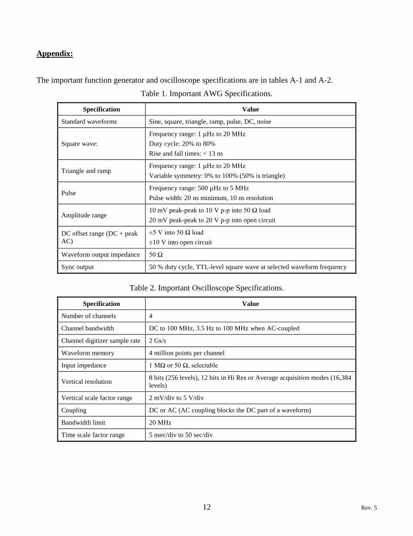
The important function generator and oscilloscope specifications are in tables A-1 and A-2.
Table 1. Important AWG Specifications.
Specification Value
Standard waveforms Sine, square, triangle, ramp, pulse, DC, noise
Square wave:
Frequency range: 1 µHz to 20 MHz
Duty cycle: 20% to 80%
Rise and fall times: < 13 ns
Triangle and ramp Frequency range: 1 µHz to 20 MHz
Variable symmetry: 0% to 100% (50% is triangle)
Pulse Frequency range: 500 µHz to 5 MHz
Pulse width: 20 ns minimum, 10 ns resolution
Amplitude range 10 mV peak-peak to 10 V p-p into 50 Ω load
20 mV peak-peak to 20 V p-p into open circuit
DC offset range (DC + peak
AC)
±5 V into 50 Ω load
±10 V into open circuit
Waveform output impedance 50 Ω
Sync output 50 % duty cycle, TTL-level square wave at selected waveform frequency
Table 2. Important Oscilloscope Specifications.
Specification Value
Number of channels 4
Channel bandwidth DC to 100 MHz, 3.5 Hz to 100 MHz when AC-coupled
Channel digitizer sample rate 2 Gs/s
Waveform memory 4 million points per channel
Input impedance 1 MΩ or 50 Ω, selectable
Vertical resolution 8 bits (256 levels), 12 bits in Hi Res or Average acquisition modes (16,384
levels)
Vertical scale factor range 2 mV/div to 5 V/div
Coupling DC or AC (AC coupling blocks the DC part of a waveform)
Bandwidth limit 20 MHz
Time scale factor range 5 nsec/div to 50 sec/div

Operational Amplifiers
EE 3401 Laboratory Exercise
Electrical Engineering Department
Kennesaw State University
1 Rev. 3
Objectives:
Students analyze, build, test, and simulate several operational amplifier (op-amp) circuits to develop a
fundamental understanding of circuits using them. Students also design an amplifier circuit to
specifications.
Introduction:
Integrated circuit (IC) Op-amps are used in many applications such as fixed- or variable-gain amplifiers,
filters, integrators, differentiators, and voltage regulators. This exercise focuses on classic op-amp
applications such as basic inverting and non-inverting amplifiers, including a cascade topology. A
potentiometer is used in two situations: to create an adjustable amplifier gain and to create an adjustable
reference voltage.
In the prelab assignment, students analyze the amplifier circuits they build and test in the lab. The prelab
assignment includes a variable-gain amplifier circuit design problem that is simulated later. The circuits
built I the lab include decoupling capacitors to help reduce interference signals that could appear on the
op-amp power supply pins.
The op-amp used is the LM741. It was very popular in the past when higher dc supply voltages were
more common. Multiple manufacturers produce the 741 op-amp and these other models have different
prefixes such as uA741. Today, many op-amps have better performance and can operate from dc
supplies of only a few volts. But the LM741 is robust and this is an important characteristic in
instructional labs when circuit connection errors occur.
Equipment:
Function/Arbitrary Waveform Generator
Oscilloscope
Digital Multimeter
DC power supply with 15 V and +5 V outputs
Cables and oscilloscope probes as needed
Solderless breadboard
Components:
Resistors (Qty): 10 k (3), 56 k (1), 100 k (1)
Potentiometer (Qty): 100 k (1)
Op-amp (Qty): LM741 (2)
Capacitors (Qty): 0.1 F (3)
Prelab:
Perform the following analyses and calculations before coming to lab. For all circuits in this assignment,
assume that the op-amps are ideal and that they use ± 15 V power supplies for biasing. Fig. 1 shows how
the op-amp’s schematic symbol maps to its physical IC pinout.
1. For the five amplifier circuits in Figs. 2, 3, 4, 5, and 6:
a. Write an expression for the output voltage, vo, in terms of the resistor symbols and the input
voltage, vin.

2 Rev. 3
• For the first and second circuits (Figs. 2 and 3), the feedback resistor is the series
combination of R2 and R3. Use both of these resistor symbols in your expression.
• For circuit 5 (Fig. 6), assume that vin = 5V and ignore potentiometer R1 and C3.
b. Using resistor values and input voltage amplitudes, calculate the peak-peak output voltage, vo
(not just the peak voltage) and numerical voltage gain vo/vin.
• Calculate three numerical gains for the circuit 2 (Fig. 3) for R3 = 30 k, 100 k, and 0
• Record these results in Table 1 for circuits 1 through 4 (Figs. 2 through 5) and in Table 2 for
the circuit 5 (Fig. 6).
2. Design an op-amp circuit that meets the following specifications. Your design can be done with one
or two op-amps. Your instructor may give you a different design.
Note: Show all work. Draw a schematic of your design and label component values and op-amp pin
numbers.
a. The op-amp circuit must have a non-inverting overall voltage gain that is adjustable from +3 to
+12. The circuit has a 47 kΩ load resistor connected from the last op-amp’s output terminal to
ground.
b. The circuit input resistance must be 50 kΩ.
c. Your design is limited to a maximum of two op-amps and seven resistors, one of which is a
variable 100 kΩ resistor (potentiometer). The potentiometer resistance is 0 when adjusted to
one extreme of its range and 100 kΩ at the other extreme.
d. When the potentiometer is adjusted to one extreme position the overall circuit voltage gain
should be +3. When the variable resistor is adjusted to its other extreme position the overall
circuit voltage gain should be +12.
Procedure:
General Information
1. This is important information about connecting the LM 741 op-amp in a circuit and making
waveform measurements.
Fig. 1. LM741 op-amp pinout looking at it from above.

3 Rev. 3
a. Refer to the LM741’s pinout drawing in Fig. 1.
Note: The Offset Null (pins 1 and 5) as well as pin 8 are left unconnected in this lab exercise.
• When constructing the circuits, you may have to combine resistors to realize the required
values as closely as you can.
• Use ± VCC = ± 15 V for all circuits; that is +V = 15V and -V = -15V. For all circuits except
circuit 3 in Fig. 4, make sure that the input voltage, vin, has no dc-offset voltage.
b. Measure sine wave input and output waveforms in peak-peak values. The oscilloscope can make
the measurements automatically. Record your data in Table 1.
Note: Use Hi Res or Average acquisition mode for best oscilloscope measurements.
Note: Always turn off both power supplies before making circuit changes.
Note: Be careful not to damage the op-amp pins when it is inserted or removed from the proto-
board. When removing, you should carefully pry it out, not pull it with your fingers. An
IC puller tool is best.
Op Amp Circuit Measurements
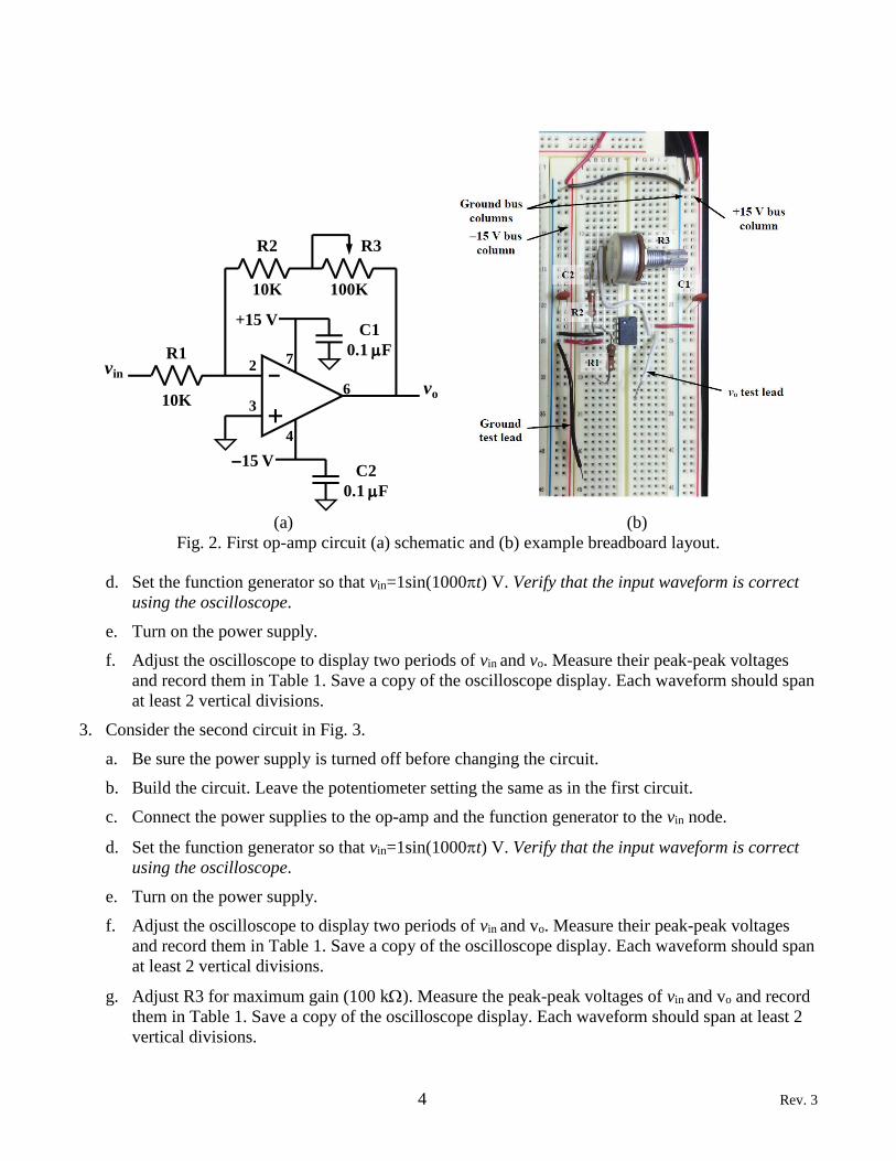
2. The circuit in first op-amp circuit in Fig. 2a uses a potentiometer in the feedback path for adjustable
gain. R1 and R2 set the minimum gain and R3 provides the adjustable gain range.
A potentiometer is a variable resistor with three terminals. The wiper is the center terminal and it
connects to the potentiometer’s internal resistance at an adjustable location set by the knob or screw.
• Let the resistance between the wiper and the left end terminal of R3 be Rx. Then the
resistance between the wiper and the right end terminal is Ry = Rmax – Rx, where Rmax is the
resistance between the two end terminals, in this case 100 k.
• Only one of the two resistances is needed in this circuit, so you will connect the wiper
terminal with a wire to left end terminal. This shorts out one of the two resistances, leaving
the other as R3 = Ry in Fig. 2a.
Note: Only use a potentiometer when adjustable gain is necessary. Otherwise use a fixed resistor.
a. Adjust the potentiometer so that the resistance from the wiper to the right end terminal is 30 k.
The view is looking at the adjusting wiper’s shaft.
b. Place the components on your breadboard. A possible layout is shown in Fig. 2b. The breadboard
busses (long connected columns) are used for the power supply connections. Connect C1
between the +15 V bus and the ground (GND) bus and one ground bus and C2 between the -15
V bus and the other ground bus. C1 and C2 should be within 1 inch of the LM741 IC.
Connect the other components. Minimize the number of wires. Always connect components
directly to each other if you can. For example, one end of R1 and R2 should connect directly to
the 741’s pin 2.
c. Connect the power supplies to the op-amp and the function generator to the vin node.
4 Rev. 3
d. Set the function generator so that vin=1sin(1000t) V. Verify that the input waveform is correct
using the oscilloscope.
e. Turn on the power supply.
f. Adjust the oscilloscope to display two periods of vin and vo. Measure their peak-peak voltages
and record them in Table 1. Save a copy of the oscilloscope display. Each waveform should span
at least 2 vertical divisions.
3. Consider the second circuit in Fig. 3.
a. Be sure the power supply is turned off before changing the circuit.
b. Build the circuit. Leave the potentiometer setting the same as in the first circuit.
c. Connect the power supplies to the op-amp and the function generator to the vin node.
d. Set the function generator so that vin=1sin(1000t) V. Verify that the input waveform is correct
using the oscilloscope.
e. Turn on the power supply.
f. Adjust the oscilloscope to display two periods of vin and vo. Measure their peak-peak voltages
and record them in Table 1. Save a copy of the oscilloscope display. Each waveform should span
at least 2 vertical divisions.
g. Adjust R3 for maximum gain (100 k). Measure the peak-peak voltages of vin and vo and record
them in Table 1. Save a copy of the oscilloscope display. Each waveform should span at least 2
vertical divisions.
(a) (b)
Fig. 2. First op-amp circuit (a) schematic and (b) example breadboard layout.
vin
+15 V
−15 V
vo
7
4
6
2
3
R2
10K
R1
10K 100K
R3
C2
0.1 F
C1
0.1 F
5 Rev. 3
h. Adjust R3 for minimum gain (0 ). Measure the peak-peak voltages of vin and vo and record
them in Table 1. Save a copy of the oscilloscope display. Each waveform should span at least 2
vertical divisions.
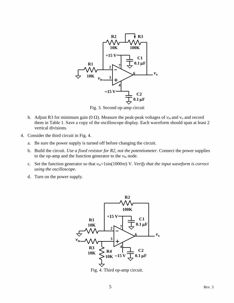
4. Consider the third circuit in Fig. 4.
a. Be sure the power supply is turned off before changing the circuit.
b. Build the circuit. Use a fixed resistor for R2, not the potentiometer. Connect the power supplies
to the op-amp and the function generator to the vin node.
c. Set the function generator so that vin=1sin(1000t) V. Verify that the input waveform is correct
using the oscilloscope.
d. Turn on the power supply.
Fig. 3. Second op-amp circuit
vin
+15 V
−15 V
vo
7
4
6
2
3
R2
10K
R1
10K 100K
R3
C2
0.1 F
C1
0.1 F
Fig. 4. Third op-amp circuit.
R2
vin
+15 V
−15 V
vo
7
4
6
2
3
R1
10K
100K
R3
10K R4
10K
C1
0.1 F
C2
0.1 F
6 Rev. 3
e. Adjust the oscilloscope to display two periods of vin and vo. Measure their peak-peak voltages
and record them in Table 1. Save a copy of the oscilloscope display. Each waveform should span
at least 2 vertical divisions.
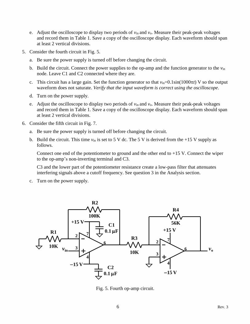
5. Consider the fourth circuit in Fig. 5.
a. Be sure the power supply is turned off before changing the circuit.
b. Build the circuit. Connect the power supplies to the op-amp and the function generator to the vin
node. Leave C1 and C2 connected where they are.
c. This circuit has a large gain. Set the function generator so that vin=0.1sin(1000t) V so the output
waveform does not saturate. Verify that the input waveform is correct using the oscilloscope.
d. Turn on the power supply.
e. Adjust the oscilloscope to display two periods of vin and vo. Measure their peak-peak voltages
and record them in Table 1. Save a copy of the oscilloscope display. Each waveform should span
at least 2 vertical divisions.
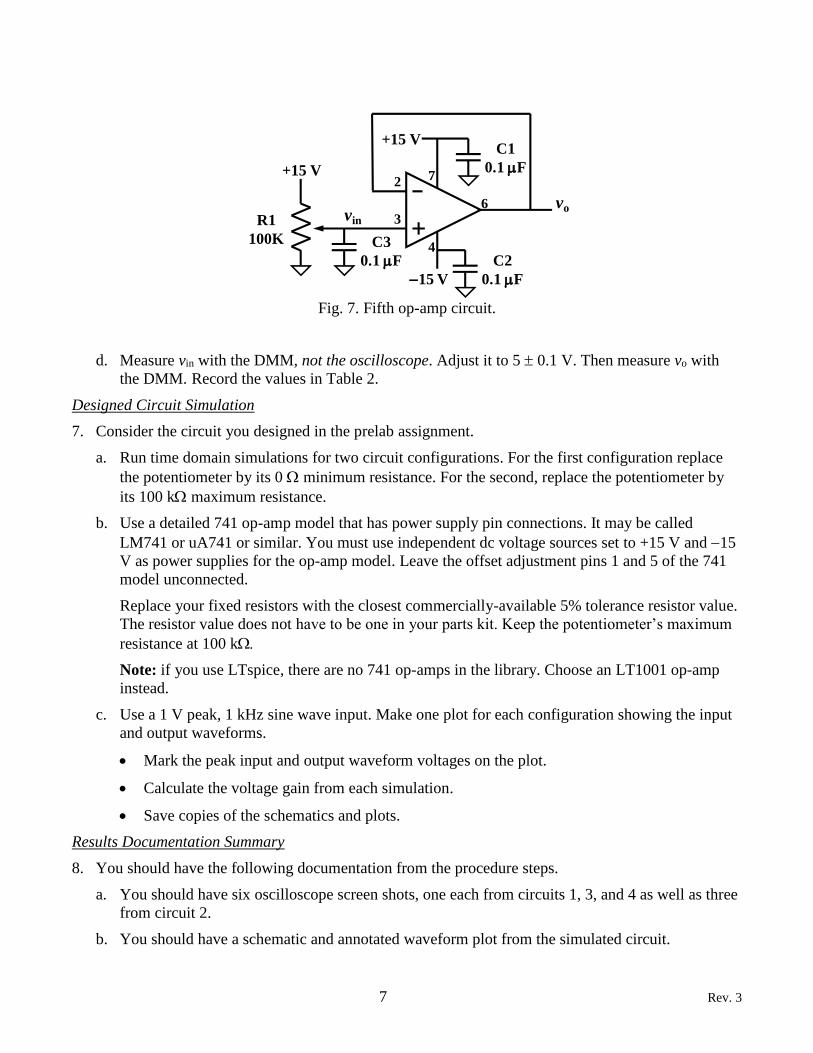
6. Consider the fifth circuit in Fig. 7.
a. Be sure the power supply is turned off before changing the circuit.
b. Build the circuit. This time vin is set to 5 V dc. The 5 V is derived from the +15 V supply as
follows.
Connect one end of the potentiometer to ground and the other end to +15 V. Connect the wiper
to the op-amp’s non-inverting terminal and C3.
C3 and the lower part of the potentiometer resistance create a low-pass filter that attenuates
interfering signals above a cutoff frequency. See question 3 in the Analysis section.
c. Turn on the power supply.
Fig. 5. Fourth op-amp circuit.
vin
+15 V
−15 V
7
4
6
2
3
R2
10K
R1
100K
+15 V
−15 V
vo
7
4
6
2
3
R4
10K
R3
56K
C2
0.1 F
C1
0.1 F
7 Rev. 3
d. Measure vin with the DMM, not the oscilloscope. Adjust it to 5 0.1 V. Then measure vo with
the DMM. Record the values in Table 2.
Designed Circuit Simulation
7. Consider the circuit you designed in the prelab assignment.
a. Run time domain simulations for two circuit configurations. For the first configuration replace
the potentiometer by its 0 minimum resistance. For the second, replace the potentiometer by
its 100 k maximum resistance.
b. Use a detailed 741 op-amp model that has power supply pin connections. It may be called
LM741 or uA741 or similar. You must use independent dc voltage sources set to +15 V and −15
V as power supplies for the op-amp model. Leave the offset adjustment pins 1 and 5 of the 741
model unconnected.
Replace your fixed resistors with the closest commercially-available 5% tolerance resistor value.
The resistor value does not have to be one in your parts kit. Keep the potentiometer’s maximum
resistance at 100 k
Note: if you use LTspice, there are no 741 op-amps in the library. Choose an LT1001 op-amp
instead.
c. Use a 1 V peak, 1 kHz sine wave input. Make one plot for each configuration showing the input
and output waveforms.
• Mark the peak input and output waveform voltages on the plot.
• Calculate the voltage gain from each simulation.
• Save copies of the schematics and plots.
Results Documentation Summary
8. You should have the following documentation from the procedure steps.
a. You should have six oscilloscope screen shots, one each from circuits 1, 3, and 4 as well as three
from circuit 2.
b. You should have a schematic and annotated waveform plot from the simulated circuit.
Fig. 7. Fifth op-amp circuit.
vin
+15 V
−15 V
vo
7
4
6
2
3
+15 V
C2
0.1 F
C1
0.1 F
R1
100K C3
0.1 F
8 Rev. 3
c. Be sure that you recorded data and calculated results in steps you were asked to.
d. Check with your instructor for additional documentation requirements.
Analysis:
1. Calculate the voltage gain using your measured data from procedure steps 1 through 6 and record the
results in Table 1. Calculate the percent error between measured and calculated gains using Eq. 1
and record it in Table 1.
% 100%measured voltage calculated voltage
errorcalculated voltage
−= (1)
2. Determine the percentage error between the ideal and simulated gain from procedure step 7.
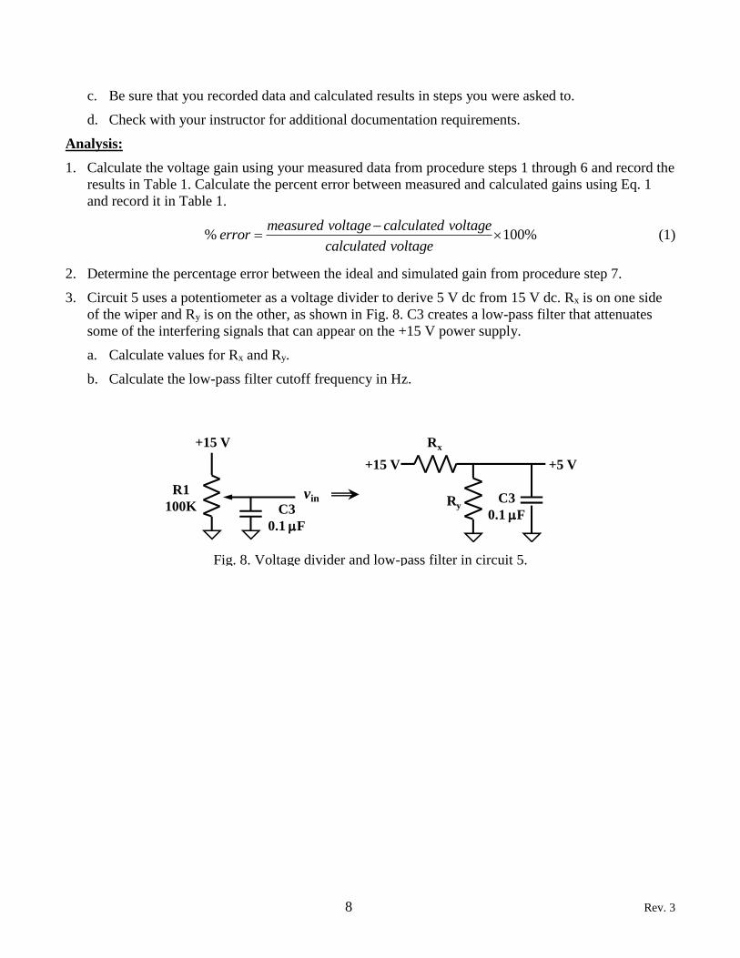
3. Circuit 5 uses a potentiometer as a voltage divider to derive 5 V dc from 15 V dc. Rx is on one side
of the wiper and Ry is on the other, as shown in Fig. 8. C3 creates a low-pass filter that attenuates
some of the interfering signals that can appear on the +15 V power supply.
a. Calculate values for Rx and Ry.
b. Calculate the low-pass filter cutoff frequency in Hz.
Fig. 8. Voltage divider and low-pass filter in circuit 5.
vin
+15 V
R1
100K
+15 V
+5 V
Rx
RyC3
0.1 F
C3
0.1 F

9 Rev. 3
Appendix:
Table 1. Calculated and measured data for circuits 1 through 4.
Circuit No. Calculated
vo (peak-peak)
Measured
vin (peak-peak)
Measured
vo (peak-peak)
Calculated
Gain (Prelab)
Measured
Gain
Gain
Percent
Error
1
2 R3 = 30 k
2 R3 = 100 k
2 R3 = 0
3
4
Table 2. Calculated and measured data for circuit 5.
Circuit No. Calculated
vo (dc)
Measured
vin (dc)
Measured
vo (dc)
Calculated
Gain (Prelab)
Measured
Gain
Gain
Percent
Error
5
Differentiator, Integrator, and Pulse-Width Modulator Circuits
Using Op Amps
EE 3401 Laboratory Exercise
Electrical Engineering Department
Kennesaw State University
1 Rev. 1
Objectives:
Students analyze, build, and test integrator, differentiator, and pulse-width modulator circuits using op
amps to develop a fundamental understanding of their operation.
Introduction:
Op amps are used in circuits to perform various mathematical operations, such as amplitude scaling
(gain), addition, subtraction, integration, and differentiation. This exercise focuses on the inverting
integrator and inverting differentiator circuits, which are used in circuits such as waveform generators,
active filters, proportional-integral-differential (PID) control systems, and pulse-width modulators
(PWM). Within these more complex systems, the individual op amp circuits are “building blocks”
connected to perform the desired system-level functions.
The PWM circuit in this exercise uses a triangle waveform produced from an integrator circuit and an op
amp configured as a voltage comparator to demonstrate the building-block design approach. Example
PWM applications include dc motor control, switched-mode power supplies, D/A and A/D converters,
and light dimmer circuits.
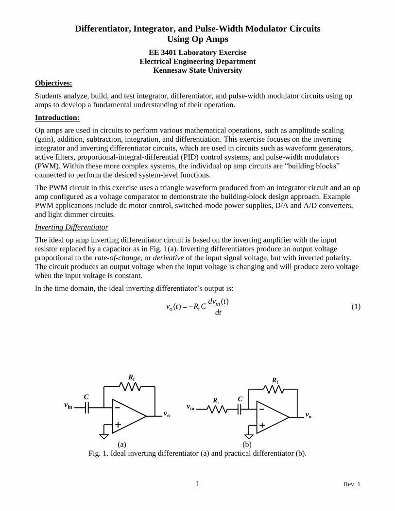
Inverting Differentiator
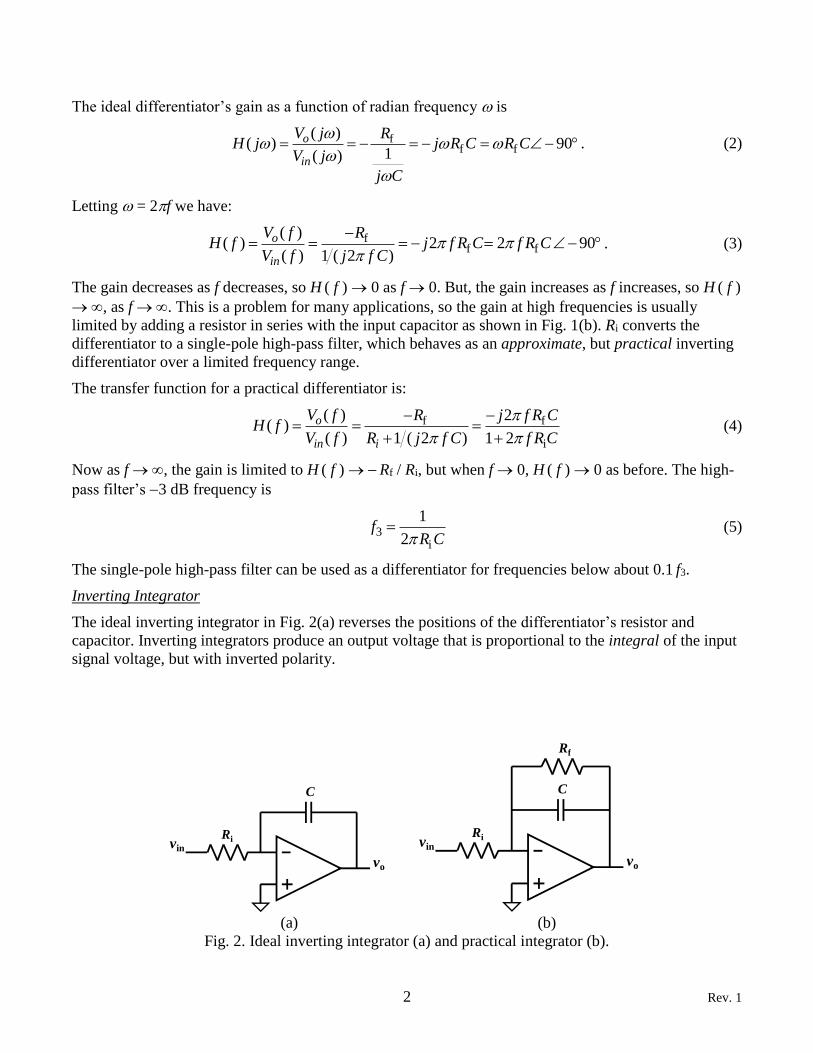
The ideal op amp inverting differentiator circuit is based on the inverting amplifier with the input
resistor replaced by a capacitor as in Fig. 1(a). Inverting differentiators produce an output voltage
proportional to the rate-of-change, or derivative of the input signal voltage, but with inverted polarity.
The circuit produces an output voltage when the input voltage is changing and will produce zero voltage
when the input voltage is constant.
In the time domain, the ideal inverting differentiator’s output is:
f
( )( ) in
o
dv tv t R C
dt= − (1)
(a) (b)
Fig. 1. Ideal inverting differentiator (a) and practical differentiator (b).
vin
vo
C
Rf
vin
vo
C
Rf
Ri
2 Rev. 1
The ideal differentiator’s gain as a function of radian frequency is
ff f
( )( ) 90
1( )
o
in
V j RH j j R C R C
V j
j C
= = − = − = − . (2)
Letting = 2f we have:
ff f
( )( ) 2 2 90
( ) 1 ( 2 )
o
in
V f RH f j f R C f R C
V f j f C
−= = = − = − . (3)
The gain decreases as f decreases, so H ( f ) → 0 as f → 0. But, the gain increases as f increases, so H ( f )
→ , as f → . This is a problem for many applications, so the gain at high frequencies is usually
limited by adding a resistor in series with the input capacitor as shown in Fig. 1(b). Ri converts the
differentiator to a single-pole high-pass filter, which behaves as an approximate, but practical inverting
differentiator over a limited frequency range.
The transfer function for a practical differentiator is:
f f
i
( ) 2( )
( ) 1 ( 2 ) 1 2
o
in i
V f R j f R CH f
V f R j f C f R C
− −= = =
+ + (4)
Now as f → , the gain is limited to H ( f ) → −Rf / Ri, but when f → 0, H ( f ) → 0 as before. The high-
pass filter’s −3 dB frequency is
3i
1
2f
R C= (5)
The single-pole high-pass filter can be used as a differentiator for frequencies below about 0.1 f3.
Inverting Integrator
The ideal inverting integrator in Fig. 2(a) reverses the positions of the differentiator’s resistor and
capacitor. Inverting integrators produce an output voltage that is proportional to the integral of the input
signal voltage, but with inverted polarity.
(a) (b)
Fig. 2. Ideal inverting integrator (a) and practical integrator (b).
vin
vo
C
Ri vin
vo
C
Ri
Rf

3 Rev. 1
In the time domain, the ideal inverting integrator’s output is:
0
i
1( ) ( ) (0)
t
o in cv t v t dt vR C
= − + (6)
Where vc(0) is the initial voltage on the capacitor at t = 0. The ideal integrator’s gain as a function of
is
i i
( ) 1 1( ) 90
( )
o
in
V jH j
V j j R C R C
= = − = . (7)
Letting = 2f gives:
i i
( ) 1 1( ) 90
( ) 2 2
o
in
V fH f
V f j f R C f R C = = − = . (8)
The ideal inverting integrator also has problems in practical applications because its gain H ( f ) → as f
→ 0. Real op amps have small dc bias currents flowing in or out of their input terminals. These bias
currents are in the pA or nA range and neglected in most applications. Bias currents in an ideal
integrator charge the feedback capacitor, causing the output voltage to drift and usually saturate.
Therefore, a resistor is connected in parallel with the feedback capacitor as shown in Fig. 2(b), providing
an alternative path for the bias current to flow. Rf converts the integrator to a single-pole low-pass filter,
which behaves as an approximate, but practical inverting integrator over a limited frequency range.
The transfer function for a practical integrator is:
f i
f
( )( )
( ) 1 2
o
in
V f R RH f
V f j f R C
−= =
+ (9)
Now as f → 0, the gain is limited to H ( f ) → −Rf / Ri, but when f → , H ( f ) → 0 as before. The low-
pass filter’s −3 dB frequency is
3f
1
2f
R C= (10)
The single-pole low-pass filter can be used as an integrator for frequencies above about 10 f3.
Pulse-Width Modulator
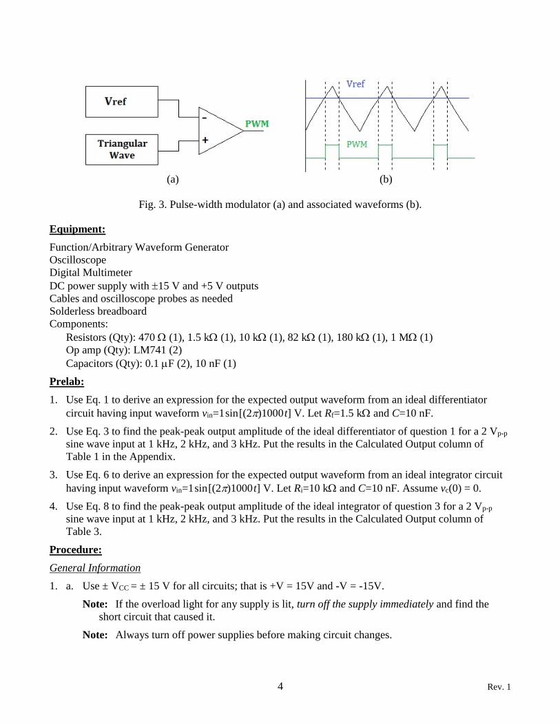
Fig. 3(a) shows a PWM circuit using an open-loop op amp as a voltage comparator. Negative feedback
is not used in comparators, but many times positive feedback is used to improve noise immunity.
A triangular waveform is applied to the non-inverting input and a variable reference voltage waveform
Vref is applied to the inverting input. Since the op amp is a differential amplifier, it compares the
triangular wave voltage with that of Vref. The comparator output is high when the voltage at the non-
inverting input is greater than Vref and the output is low when the voltage at the non-inverting input is
less than Vref.
When Vref changes, the pulse width of the output changes. Fig. 3(b) shows the superimposed triangular
and dc Vref input waveforms and the resulting output PWM waveform from the comparator.
4 Rev. 1
Equipment:
Function/Arbitrary Waveform Generator
Oscilloscope
Digital Multimeter
DC power supply with 15 V and +5 V outputs
Cables and oscilloscope probes as needed
Solderless breadboard
Components:
Resistors (Qty): 470 (1), 1.5 k (1), 10 k (1), 82 k (1), 180 k (1), 1 M (1)
Op amp (Qty): LM741 (2)
Capacitors (Qty): 0.1 F (2), 10 nF (1)
Prelab:
1. Use Eq. 1 to derive an expression for the expected output waveform from an ideal differentiator
circuit having input waveform vin=1sin[(2)1000t] V. Let Rf=1.5 k and C=10 nF.
2. Use Eq. 3 to find the peak-peak output amplitude of the ideal differentiator of question 1 for a 2 Vp-p
sine wave input at 1 kHz, 2 kHz, and 3 kHz. Put the results in the Calculated Output column of
Table 1 in the Appendix.
3. Use Eq. 6 to derive an expression for the expected output waveform from an ideal integrator circuit
having input waveform vin=1sin[(2)1000t] V. Let Ri=10 k and C=10 nF. Assume vc(0) = 0.
4. Use Eq. 8 to find the peak-peak output amplitude of the ideal integrator of question 3 for a 2 Vp-p
sine wave input at 1 kHz, 2 kHz, and 3 kHz. Put the results in the Calculated Output column of
Table 3.
Procedure:
General Information
1. a. Use ± VCC = ± 15 V for all circuits; that is +V = 15V and -V = -15V.
Note: If the overload light for any supply is lit, turn off the supply immediately and find the
short circuit that caused it.
Note: Always turn off power supplies before making circuit changes.
(a) (b)
Fig. 3. Pulse-width modulator (a) and associated waveforms (b).
5 Rev. 1
b. Use 0.1 F decoupling capacitors C2 and C3 between each power supply and ground.
c. Measure input and output waveforms in peak-peak values. The oscilloscope can make the
measurements automatically.
d. Leave LM741 pins 1, 5, and 8 unconnected.
Note: Be careful not to damage the op amp pins when it is inserted or removed from the
breadboard. When removing, you should carefully pry it out, not pull it with your fingers. An
IC puller tool is best.
e. Use Hi Res or Average acquisition mode for best oscilloscope measurements.
Inverting Differentiator Measurements
2. In the first part of this procedure you will observe the inverting differentiator’s response to different
types of input waveforms. In the second part you will see how it responds as a sine wave input’s
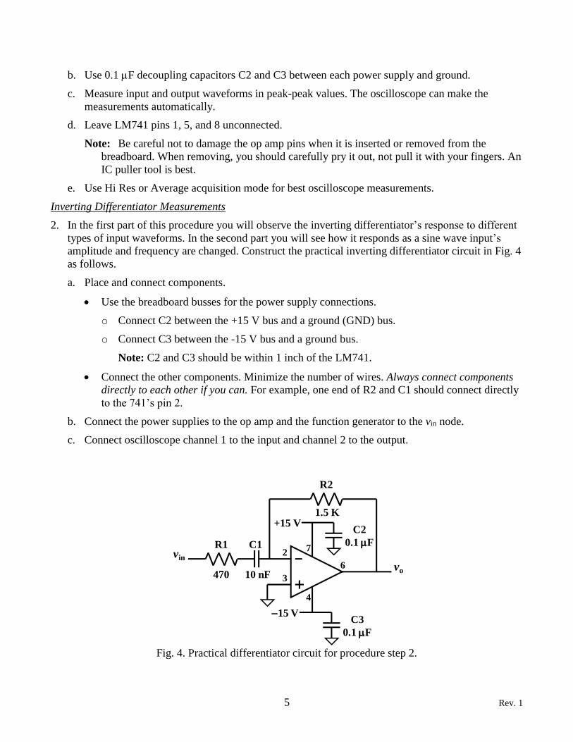
amplitude and frequency are changed. Construct the practical inverting differentiator circuit in Fig. 4
as follows.
a. Place and connect components.
• Use the breadboard busses for the power supply connections.
o Connect C2 between the +15 V bus and a ground (GND) bus.
o Connect C3 between the -15 V bus and a ground bus.
Note: C2 and C3 should be within 1 inch of the LM741.
• Connect the other components. Minimize the number of wires. Always connect components
directly to each other if you can. For example, one end of R2 and C1 should connect directly
to the 741’s pin 2.
b. Connect the power supplies to the op amp and the function generator to the vin node.
c. Connect oscilloscope channel 1 to the input and channel 2 to the output.
Fig. 4. Practical differentiator circuit for procedure step 2.
R2
vin
vo
C1
1.5 K
470
−15 V
4
C3
0.1 F
2
3
+15 V
7
C2
0.1 FR1
10 nF6

6 Rev. 1
d. Turn on the power supply.
e. Set the function generator so that vin=1sin[(2)1000t] V. Verify that the input waveform is
correct using the oscilloscope. Adjust the oscilloscope to display two periods of vin and vo.
f. Describe the output waveform as it relates to the input and record your description in Table 1.
You do not have to record the amplitudes.
• For example, if the input waveform was a cosine, you would describe the output of a non-
inverting differentiator as “inverted sine” or “−sine”.
o Remember that this is an inverting differentiator.
• For the sine wave input only, record the phase difference between the output and input
waveforms in degrees and indicate whether the output is leading or lagging.
• Save an image of the oscilloscope display.
g. Repeat step (f) for the other waveforms in Table 1. Be sure to save oscilloscope display images.
i. Set the function generator so that vin=1sin[(2)1000t] V. Verify that the input waveform is
correct using the oscilloscope. Adjust the oscilloscope to display two periods of vin and vo.
j. Record the output voltage in Table 2. You do not need to record the phase difference between
input and output waveforms. You do not need to save oscilloscope display images.
k. Repeat the measurement for the other input amplitude and frequency settings in Table 2.
l. Turn off the power supply. Leave the power supply connected to the op amp.
Inverting Integrator Measurements
3. In the first part of this procedure you will observe the inverting integrator’s response to different
types of input waveforms. In the second part you will see how it responds as a sine wave input’s
amplitude and frequency are changed. Construct the practical inverting integrator circuit in Fig. 5 as
follows.
a. Place and connect components. Minimize the number of wires. Always connect components
directly to each other if you can. For example, one end of R1, R2 and C1 should connect directly
to the 741’s pin 2.
b. Connect the function generator to the vin node.
c. Connect oscilloscope channel 1 to the input and channel 2 to the output.
d. Turn on the power supply.
e. Set the function generator so that vin=1sin[(2)1000t] V. Verify that the input waveform is
correct using the oscilloscope. Adjust the oscilloscope to display two periods of vin and vo.
f. Describe the output waveform as it relates to the input and record your description in Table 3.
You do not have to record the amplitudes.
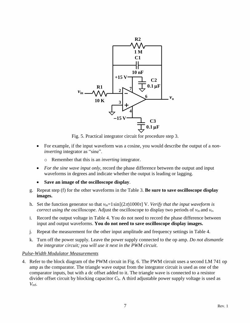
7 Rev. 1
• For example, if the input waveform was a cosine, you would describe the output of a non-
inverting integrator as “sine”.
o Remember that this is an inverting integrator.
• For the sine wave input only, record the phase difference between the output and input
waveforms in degrees and indicate whether the output is leading or lagging.
• Save an image of the oscilloscope display.
g. Repeat step (f) for the other waveforms in the Table 3. Be sure to save oscilloscope display
images.
h. Set the function generator so that vin=1sin[(2)1000t] V. Verify that the input waveform is
correct using the oscilloscope. Adjust the oscilloscope to display two periods of vin and vo.
i. Record the output voltage in Table 4. You do not need to record the phase difference between
input and output waveforms. You do not need to save oscilloscope display images.
j. Repeat the measurement for the other input amplitude and frequency settings in Table 4.
k. Turn off the power supply. Leave the power supply connected to the op amp. Do not dismantle
the integrator circuit; you will use it next in the PWM circuit.
Pulse-Width Modulator Measurements
4. Refer to the block diagram of the PWM circuit in Fig. 6. The PWM circuit uses a second LM 741 op
amp as the comparator. The triangle wave output from the integrator circuit is used as one of the
comparator inputs, but with a dc offset added to it. The triangle wave is connected to a resistor
divider offset circuit by blocking capacitor Cb. A third adjustable power supply voltage is used as
Vref.
Fig. 5. Practical integrator circuit for procedure step 3.
R2
vin
vo
C1
1 M
10 K
−15 V
4
C3
0.1 F
2
3
+15 V
7
C2
0.1 FR1
10 nF
6
8 Rev. 1
a. Temporarily disable the function generator’s output or disconnect it from the integrator’s input.
b. Place a second LM 741 op amp on the breadboard. You must connect its power supply pins to
15 V.
c. Connect one lead of 0.1 F capacitor Cb to the comparator’s pin 3 and the other lead to the
integrator circuit’s output.
d. Create a voltage divider between +15 V and ground. Use a 1 M resistor for R1. R2 is a series
combination of a 180 k and a 82 k resistor. Do not connect it to Cb or the comparator yet.
• Calculate the expected voltage across R2. Measure it with the DMM and verify that it is
within 10 % of the calculated value. Record the calculated and measured values below.
Calculated R2 voltage: Measured R2 voltage:
• Now connect the voltage divider output to the junction of Cb and comparator pin 3.
e. Set the function generator for a 500 Hz, 1.0 Vp-p square wave (50% symmetry pulse).
• Connect the function generator’s output to the integrator. Measure the peak-peak voltage at
the integrator’s output using oscilloscope channel 1 and record it below.
Integrator output voltage (peak-peak):
f. Measure the waveform on the right side of Cb with channel 2.
• Use cursors to find the maximum and minimum voltages of the offset triangle wave on
channel 2.
• Save an oscilloscope screen image.
Note: The lowest voltage of the triangle wave should be greater than 0 V. Check the circuit for
errors if it is not.
g. Set up the oscilloscope so the comparator input and output waveforms can be observed using
three channels.
• Channel 1:
o Connect it to the node with the offset triangle wave on the right of Cb.
o Set the vertical scale to 1 V/div.
Fig. 6. PWM circuit for procedure step 4.

9 Rev. 1
o Move the channel 1 reference to the first vertical division above the bottom.
o dc-couple the channel.
• Trigger the oscilloscope on channel 1 or the function generator’s sync pulse.
• Channel 2:
o Use a probe. If the probe’s scale factor is selectable, make sure it is on 10. If the
oscilloscope does not automatically read the probe’s scale factor, change it in the channel
menu.
o Connect it to the comparator’s output PWM waveform.
o Set the vertical scale to 10 V/div.
o Move the channel 2 reference to the second vertical division from the top.
o dc-couple the channel.
• Channel 3:
o Connect it to Vref.
o Set the vertical scale to 1 V/div.
o Move the channel 3 reference to the first vertical division above the bottom.
o dc-couple the channel.
g. Adjust Vref to create the comparator output’s duty cycle to the values in Table 5.
• Record the Vref value in the table.
• Save an oscilloscope screen image for 25 % and 75 % duty cycles.
5. Results documentation summary.
a. You should have ten oscilloscope screen shots, four for the differentiator, three for the integrator,
and three for the pulse-width modulator.
b. Be sure that you recorded data and calculated results in steps you were asked to.
c. Check with your instructor for additional documentation requirements.
Analysis:
1. Use Eq. 11 to calculate the percent error between measured and calculated differentiator output
amplitudes for 2 Vp-p sine wave input voltages at 1 kHz, 2 kHz, and 3 kHz and put the results in the
last column of Table 2.
% 100%measured voltage calculated voltage
errorcalculated voltage
−= (11)
2. Calculate the percent error between measured and calculated integrator output amplitudes for 2 Vp-p
sine wave input voltages at 1 kHz, 2 kHz, and 3 kHz and put the results in the last column of Table
4.
3. Explain how the expression calculated in prelab question 1 relates to the differentiator’s output phase
difference recorded in Table 1, row 1.

10 Rev. 1
4. Explain how the expression calculated in prelab question 1 relates to the integrator’s output phase
difference recorded in Table 3, row 1.
5. From the measured data in Table 2, what is the dependence of the output amplitude on the signal
frequency?
6. From the measured data in Table 2, what is the dependence of the output amplitude on the input
signal’s amplitude?
7. From the measured data in Table 4, what is the dependence of the output amplitude on the signal
frequency?
8. From the measured data in Table 4, what is the dependence of the output amplitude on the input
signal’s amplitude?
9. Use Eq. 5 to calculate the high-pass −3dB frequency for the practical differentiator. Then calculate
the ratio of the worst-case (highest) signal frequency you used to the high-pass f3 frequency. Does it
meet the criterion for using a single-pole high-pass filter as a differentiator?
10. Use Eq. 10 to calculate the low-pass −3dB frequency for the practical integrator. Then calculate the
ratio of the worst-case (lowest) signal frequency you used to the low-pass f3 frequency. Does it meet
the criterion for using a single-pole low-pass filter as an integrator?

11 Rev. 1
Appendix:
Table 1. Differentiator input and output waveform descriptions
Input Waveform
Description Output Waveform Description
Phase
Difference
Sine wave
Square wave
Triangle (ramp with
50% symmetry)
Sawtooth (ramp with
25% symmetry)
Table 2. Differentiator sinusoidal input and output waveform measurements
Frequency Input Voltage
(peak-peak)
Calculated Output
Voltage
(peak-peak)
Measured Output
Voltage
(peak-peak)
Percent
Error
1 kHz
2
4
5
2 kHz
2
4
5
3 kHz
2
4
5

12 Rev. 1
Table 3. Integrator input and output waveform descriptions
Input Waveform
Description Output Waveform Description
Phase
Difference
Sine wave
Square wave
Ramp (0 % symmetry)
Table 4. Integrator sinusoidal input and output waveform measurements
Frequency Input Voltage
(peak-peak)
Calculated Output
Voltage
(peak-peak)
Measured Output
Voltage
(peak-peak)
Percent
Error
1 kHz
2
4
5
2 kHz
2
4
5
3 kHz
2
4
5

13 Rev. 1
Table 5. PWM duty cycle vs. reference voltage.
Duty Cycle Reference Voltage,
Vref
5%
25%
50%
75%
95%

Diode Characteristics
EE 3401 Laboratory Exercise
Electrical Engineering Department
Kennesaw State University
1 Rev. 9
Objectives:
Students analyze, build, and test simple circuits using typical p-n junction diodes to better understand
diode behavior. MATLAB is used to match an exponential function to measured diode current vs.
voltage data, allowing comparison to calculated values.
Introduction:
Diodes are the fundamental semiconductor device. Understanding their behavior provides a foundation
for investigating more complex devices and non-linear circuits. There are various types of diodes, such
as p-n junction diode, Schottky diode, Zener diode, etc. In this lab exercise, you will investigate the
behavior of p-n junction diodes and perform circuit analysis using the diode equation and the simplified
constant voltage drop (CVD) model.
MATLAB curve-fitting capability is used to obtain a best-fit exponential function to the measured diode
current vs. voltage data. The resulting exponential function’s parameters are used to determine the
diode’s reverse saturation current Is and emission coefficient n.
Equipment:
Agilent (Keysight) 34410A digital multimeter (DMM)
Agilent (Keysight) DSO 5014A oscilloscope or second DMM
DC power supply with 20 V and +6 V outputs
Cables and oscilloscope probes as needed
Solderless breadboard
Components:
Resistors (Qty): 330 (1), 1.0 k (1)
Diodes (Qty): 1N4007 (3)
Prelab:
1. For the circuit in Fig. 2:
Use Shockley’s equation (Eq. 1) to solve for the diode current as a function of the diode voltage and
fill in the “Diode Equation” column in Table 1.
( )1D Tv nVD Si I e= − (1)
Where vD = voltage across the diode.
Is = reverse saturation current. Let Is = 15 10-9 A.
n = emission coefficient. Let n = 2.
VT = thermal voltage. Let VT = 26 mV.
Note: These parameters are realistic for a typical 1N4007 diode over the vD measurement range in
this experiment.
2 Rev. 9
2. Using the constant voltage drop model:
Complete the Prelab Calculations columns of Table 2 assuming the diode is characterized by the
CVD model transfer curve given in Fig. 1.
3. For the circuit in Fig. 5:
Complete the Prelab Calculations columns of Table 3 for the dc input voltages indicated assuming
the diodes behave as in Fig. 1. In the columns labeled D1, D2, and D3 list the bias condition of the
specified diode (“F” for forward biased and “R” for reverse biased).
You may find it useful to redraw the circuit and add dc voltage sources or grounds for v1, v2, and v3.
Procedure:
General Information
1. When measuring the current-voltage characteristics of a diode in the next section, a DMM is used
for dc current measurement and an oscilloscope for dc voltage measurements. If available, a second
DMM would be a better choice to measure dc voltage.
Instructions refer to settings for an Agilent 34410A DMM.
Instructions refer to settings for an Agilent DSO 5014A oscilloscope. This oscilloscope can measure
average voltage automatically.
Alternatively, the dc current can be obtained from the voltage across the 330 series resistor, so a
single DMM can be used to measure diode current and voltage. Measure the 330 resistor value so
the calculated current value is more accurate.
2. When using the oscilloscope for dc voltage measurements, use Hi Res or Average acquisition mode
and use the smallest V/div scale factor that keeps the trace on the screen.
Current-Voltage Characteristics of a Typical Diode
3. You will construct the circuit in Fig. 3 on your protoboard to measure the forward diode
characteristic, but not just yet. Read the information below and set up the test instruments for the
measurement first.
Fig. 1. Diode constant-voltage drop
(CVD) model transfer curve.
Fig. 2. Circuit for measuring the forward diode
characteristic.
vD
iD
330Ω
++
−
VS
vR+ −
3 Rev. 9
a. The lab dc power supply has three adjustable outputs: 0 to +6 V, 0 to +20 V and 0 to −20 V. VS
in Fig. 3 uses the +6 V output. The black COM terminal serves as the reference for all three and
the circuit’s 0V ground.
Set up the power supply as follows.
• Make sure nothing is connected to its terminals.
• Push the +6 V button in the Meter section so that the meter will monitor that supply voltage
and current.
Note: The three buttons in the meter section select the supply the meter monitors; they do
not turn that supply on or off. The power switch turns all supplies on or off.
• Set the +6 V and ±20 V to 0 V by turning their control knobs fully counterclockwise. Turn
the Tracking Ratio knob fully clockwise.
• Turn off the power supply.
b. Configure the oscilloscope to measure vD on Ch. 1. Use the following settings.
• Ch. 1 menu: choose DC coupling and BW Limit.
• Vertical scale: select 100 mV/div.
• Horizontal scale: select some convenient value like 1 ms/div.
• In the Trigger > Mode/Coupling menu: select Auto.
Note: You cannot use Normal triggering because the oscilloscope will not trigger on the dc
waveform (except for noise artifacts); and it will not display a trace if it cannot trigger.
• In the Waveform>Acquire menu: choose Hi Res or Average, whichever results in the least
noise on the trace.
• In the Quick Meas menu select Source > Ch. 1 and Measure > Average.
Note: The average value is the dc value.
c. Configure the as an ammeter to measure iD. This requires connecting to the meter red I and black
LO terminals as in Fig. 4.
Fig. 3. Circuit for measuring the diode forward characteristic.
vD
iD
330Ω
++
−
VS
vR+ −
A
DMM as
Ammeter
Red Black
Oscilloscope
Channel 16 V
Variable
Supply

4 Rev. 9
Note: The ammeter must be connected in series with the current path. Never connect an
ammeter in parallel with a component.
• Choose dc current mode by pressing and releasing Shift, then pressing DC I, which appears
above the DC V button.
Have your instructor verify the ammeter location and operating mode are correct.
d. Build the Fig. 3 circuit using a 1N4007 diode. Include the multimeter/ammeter. Minimize the
number of wires to avoid mistakes. Connect oscilloscope channel 1 across the diode with the
ground lead connected to common.
4. Measure the diode forward transfer characteristics as follows.
a. Turn on the power supply.
b. Adjust VS to set vD as measured on the oscilloscope to the values in Table 1 as accurately as
possible. Start with vD = 0.7 V first so you can check that your measurements are OK. Record iD
from the meter and vD from the oscilloscope.
Note: Do not set your power supply voltage to the column 1 vD values. Your power supply
voltage settings will be higher than vD due to the voltage drop through the resistor. The
exception is row 1.
The Constant Voltage Drop Model
5. The circuit of Fig. 3 is also used in this part. VS uses the +6 V output of the DC power supply.
a. Turn off the power supply.
b. Turn the +6 V control knob fully counterclockwise, setting it to 0 V.
c. For the first four rows, adjust the supply to the values in the first column. Each time, record vD,
iD. and vR in Table 2. Where vR = VS − vD.
d. For the last two rows, you must reverse the polarity of the +6 V supply to create negative
voltages. Just switch the two cables on the +6 V and COM connectors. Measure the diode
voltage with the oscilloscope and then remove the oscilloscope connection and measure the
current. Do not measure current; assume it 0.
Note: The oscilloscope input impedance is much less than that of the reverse-biased diode. It
appears in parallel with the diode, so leaving the oscilloscope connection in place when
making the current measurement is a mistake. In fact, the typical ammeter is not capable of
Fig. 4. Multimeter configured as an ammeter to measure DC current.

5 Rev. 9
measuring the actual reverse biased diode current, so these values are 0 as far as this
experiment is concerned.
Large-Signal Diode Characteristics
6. Construct the circuit in Fig. 5 and measure its performance as follows. The power supply COM
terminal is the measurement ground reference.
a. Turn off the power supply.
b. Assemble the circuit on the breadboard.
c. Connect the +6 V, +20 V, −20 V and COM terminals to the breadboard binding posts. Then
connect wires from the binding posts to the circuit so that you can connect the appropriate
voltages to the diodes.
d. Monitor the output voltage with the multimeter connected as a DC voltmeter. Select the DCV
mode by pressing that button.
e. Measure the output voltage vO for the input voltages v1, v2, and v3 of Table 3.
Note: You need to change the tracking ratio to get a negative voltage from the −20V supply
with magnitude less than that of the +20V supply. Set the positive voltage to the desired
value, then while monitoring the negative voltage, change the tracking ratio until you reach
the desired value. The magnitude of the negative voltage is always less than or equal to the
magnitude of the positive voltage.
7. Results documentation summary.
a. Be sure that you recorded data and calculated results in steps you were asked to.
b. Check with your instructor for additional documentation requirements.
Fig. 5. Large-signal diode circuit
v1
+6 V
1kΩ
+
−
v2
v3
vo
D1
D2
D3

6 Rev. 9
Analysis:
1. For this question, you will plot three diode characteristics. One is the calculated data from Eq. 1, the
second is the measured data, and the third is an exponential curve that is fit to the measured data.
Refer to the partial MATLAB file in the appendix. The file has zero-filled arrays vdmeas and idmeas
for measured vD, and iD data. Replace the data in those arrays with your measured data from Table 1.
The program uses the “exp1” exponential fitting function to create an exponential function to match
your data as closely as possible. The resulting fitted function is given by Eq. 2, where the a and b
terms are found by the algorithm.
bxf ae= (2)
Once the fitting function is calculated, the program creates an array vd1 of finely-spaced voltage
points from 0 V to 0.7 V. Then the program uses Eq. 2 to find the fitted current array id1.
The program plots the measured data (idmeas vs. vdmeas) as ‘o’ points and the fitted current array
id1.
Add statements to the program to calculate Eq. 1 using the voltage array vd1 as input. Call your
array of currents idcalc. Modify the plot statement so all three curves are plotted. Fig. B-1 is an
example plot.
Generate the plot and indicate which curve is from Eq. 1.
Compare the curves and account for differences.
2. In the MATLAB command window, after running the curve matching and plotting code, type “f” at
the prompt followed by Enter. The a and b values of Eq. 2 are displayed. Use these values to find
estimates of the reverse saturation current IS and the emission coefficient n. Let VT = 26 mV.
3. Compare the calculated CVD model values and the measured values for the diode current iD of Table
2 by calculating the % error with the theoretical values as reference (Eq. 3). Put the percent errors
with 2 digits of precision in the last column of Table 2. Explain the errors.
% 100%Measured Theoretical
ErrorTheoretical
−= (3)
4. Consider the Table 3 data. Explain why the three diodes are biased the way they are for the case
where the input voltages are 12V, 0V, and 6V and the case where the inputs are all 12V.

7 Rev. 9
Appendix 1: Data Tables
Table 1. 1N4007 forward-bias characteristics.
Nominal
vD (V)
Diode Equation
iD (mA)
Measured
vD (V)
Measured
iD (mA)
0
0.2
0.4
0.45
0.5
0.55
0.6
0.65
0.7
8 Rev. 9
Table 2. Series diode circuit measurements and the CVD model data.
Prelab Calculations Experimental
VS (V)
CVD
Model
vD (V)
CVD
Model
vR (V)
CVD
Model
iD (mA)
Measured
vD (V)
Calculated
vR (V)
Measured
iD (mA)
iD Percent
Error
(Eq. 3)
0.5
1
5
-1.0 Omit 0 Omit
-5.0 Omit 0 Omit
Table 3. Large signal diode circuit data.
Input Voltages Prelab Calculations Experimental
v1 (V) v2 (V) v3 (V) D1 Bias
(expected)
D2 Bias
(expected)
D3 Bias
(expected)
vo
Calculated
vo
Measured
0 0 0
-12 6 12
12 0 6
12 12 12
-8 12 0
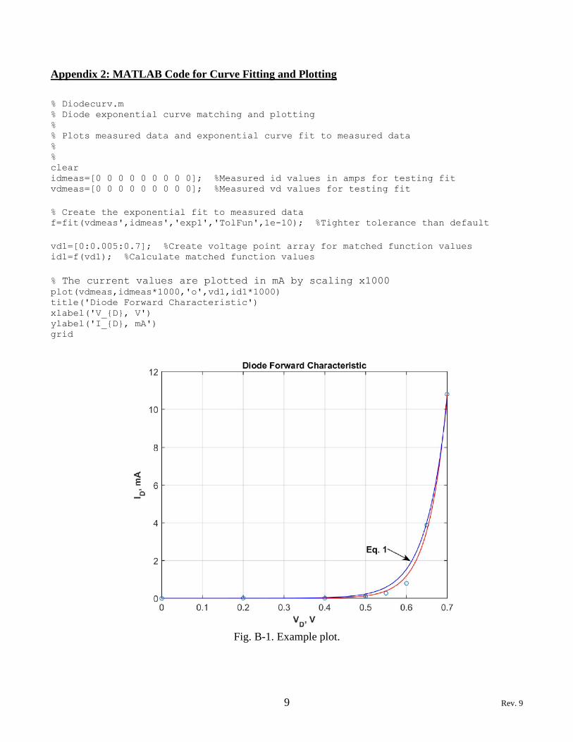
9 Rev. 9
Appendix 2: MATLAB Code for Curve Fitting and Plotting
% Diodecurv.m % Diode exponential curve matching and plotting % % Plots measured data and exponential curve fit to measured data % % clear idmeas=[0 0 0 0 0 0 0 0 0]; %Measured id values in amps for testing fit vdmeas=[0 0 0 0 0 0 0 0 0]; %Measured vd values for testing fit
% Create the exponential fit to measured data f=fit(vdmeas',idmeas','exp1','TolFun',1e-10); %Tighter tolerance than default
vd1=[0:0.005:0.7]; %Create voltage point array for matched function values id1=f(vd1); %Calculate matched function values
% The current values are plotted in mA by scaling x1000
plot(vdmeas,idmeas*1000,'o',vd1,id1*1000) title('Diode Forward Characteristic') xlabel('V_D, V') ylabel('I_D, mA') grid
Fig. B-1. Example plot.
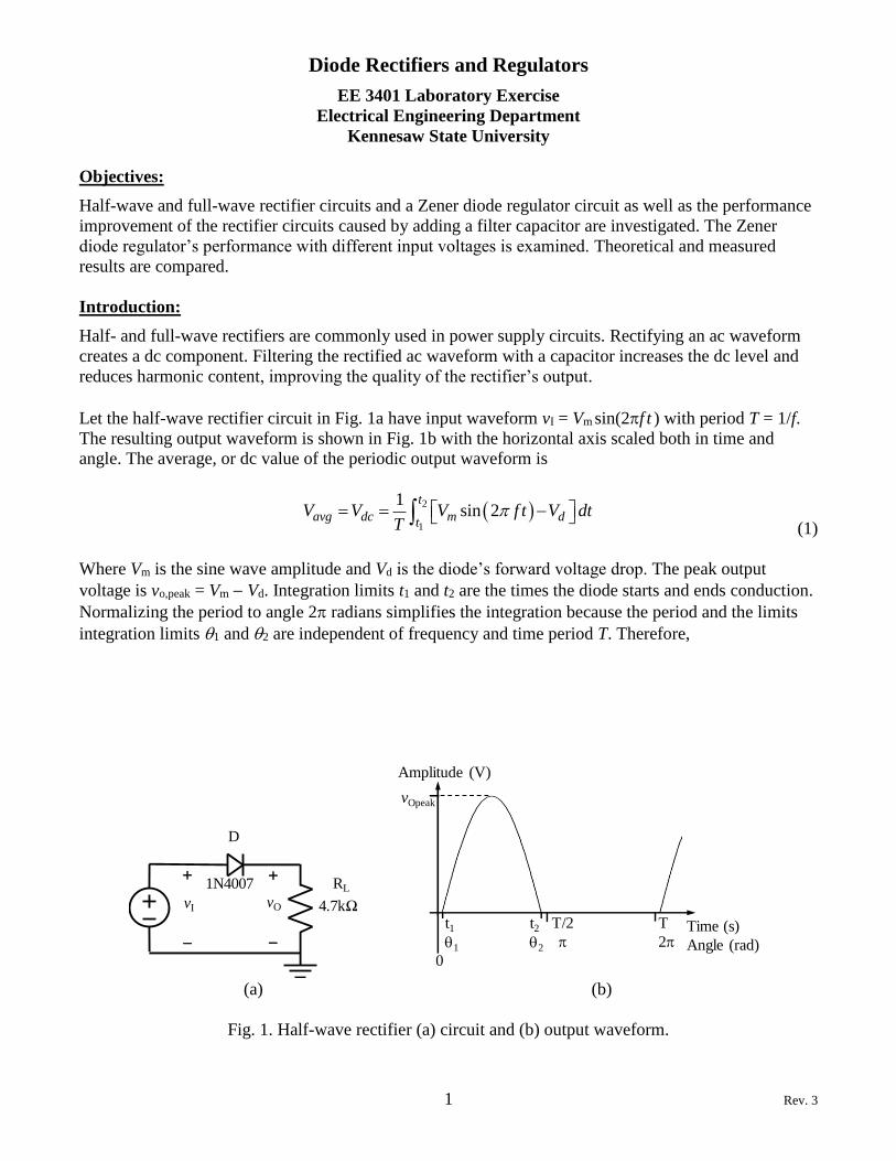
Diode Rectifiers and Regulators
EE 3401 Laboratory Exercise
Electrical Engineering Department
Kennesaw State University
1 Rev. 3
Objectives:
Half-wave and full-wave rectifier circuits and a Zener diode regulator circuit as well as the performance
improvement of the rectifier circuits caused by adding a filter capacitor are investigated. The Zener
diode regulator’s performance with different input voltages is examined. Theoretical and measured
results are compared.
Introduction:
Half- and full-wave rectifiers are commonly used in power supply circuits. Rectifying an ac waveform
creates a dc component. Filtering the rectified ac waveform with a capacitor increases the dc level and
reduces harmonic content, improving the quality of the rectifier’s output.
Let the half-wave rectifier circuit in Fig. 1a have input waveform vI = Vm sin(2f t ) with period T = 1/f.
The resulting output waveform is shown in Fig. 1b with the horizontal axis scaled both in time and
angle. The average, or dc value of the periodic output waveform is
( )2
1
1sin 2
t
avg dc m dtV V V f t V dt
T = = −
(1)
Where Vm is the sine wave amplitude and Vd is the diode’s forward voltage drop. The peak output
voltage is vo,peak = Vm − Vd. Integration limits t1 and t2 are the times the diode starts and ends conduction.
Normalizing the period to angle 2 radians simplifies the integration because the period and the limits
integration limits 1 and 2 are independent of frequency and time period T. Therefore,
(a) (b)
Fig. 1. Half-wave rectifier (a) circuit and (b) output waveform.
vI 4.7kΩ
+
−
vO
+
−
RL
D
1N4007
0
t11
T
2Time (s)
Angle (rad)
Amplitude (V)
vOpeak
t22
T/2
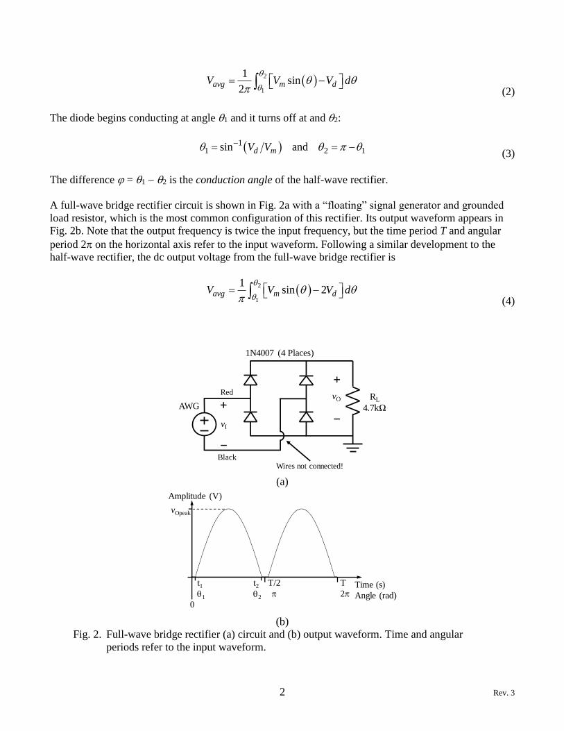
2 Rev. 3
( )2
1
1sin
2avg m dV V V d
= −
(2)
The diode begins conducting at angle 1 and it turns off at and 2:
( )1
1 2 1sin andd mV V −= = − (3)
The difference = 1 − 2 is the conduction angle of the half-wave rectifier.
A full-wave bridge rectifier circuit is shown in Fig. 2a with a “floating” signal generator and grounded
load resistor, which is the most common configuration of this rectifier. Its output waveform appears in
Fig. 2b. Note that the output frequency is twice the input frequency, but the time period T and angular
period 2 on the horizontal axis refer to the input waveform. Following a similar development to the
half-wave rectifier, the dc output voltage from the full-wave bridge rectifier is
( )2
1
1sin 2avg m dV V V d
= −
(4)
(a)
(b)
Fig. 2. Full-wave bridge rectifier (a) circuit and (b) output waveform. Time and angular
periods refer to the input waveform.
+
−
vO
1N4007 (4 Places)
vI
+
−
Wires not connected!
Red
Black
AWGRL
4.7kΩ
vOpeak
0
Amplitude (V)
t11
t22
T
2Time (s)
Angle (rad)
T/2
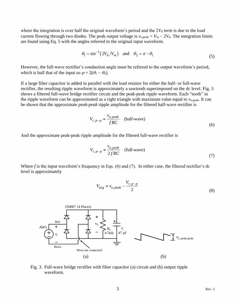
3 Rev. 3
where the integration is over half the original waveform’s period and the 2Vd term is due to the load
current flowing through two diodes. The peak output voltage is vo,peak = Vm − 2Vd. The integration limits
are found using Eq. 5 with the angles referred to the original input waveform.
( )1
1 2 1sin 2 andd mV V −= = − (5)
However, the full-wave rectifier’s conduction angle must be referred to the output waveform’s period,
which is half that of the input so = 2(1 − 2).
If a large filter capacitor is added in parallel with the load resistor for either the half- or full-wave
rectifier, the resulting ripple waveform is approximately a sawtooth superimposed on the dc level. Fig. 3
shows a filtered full-wave bridge rectifier circuit and the peak-peak ripple waveform. Each “tooth” in
the ripple waveform can be approximated as a right triangle with maximum value equal to vo,peak. It can
be shown that the approximate peak-peak ripple amplitude for the filtered half-wave rectifier is
,, (half-wave)
o peakr p p
vV
f RC−
(6)
And the approximate peak-peak ripple amplitude for the filtered full-wave rectifier is
,, (full-wave)
2
o peakr p p
vV
f RC−
(7)
Where f is the input waveform’s frequency in Eqs. (6) and (7). In either case, the filtered rectifier’s dc
level is approximately
,,
2
r p pavg o peak
VV v
− −
(8)
(a) (b)
Fig. 3. Full-wave bridge rectifier with filter capacitor (a) circuit and (b) output ripple
waveform.
RL
4.7kΩ
+
−
vO
1N4007 (4 Places)
vI
+
−
Wires not connected!
Red
Black
+
C
47 µF
AWG
vr, peak-peak
Fig. 6. Approximate full-wave rectifier ripple
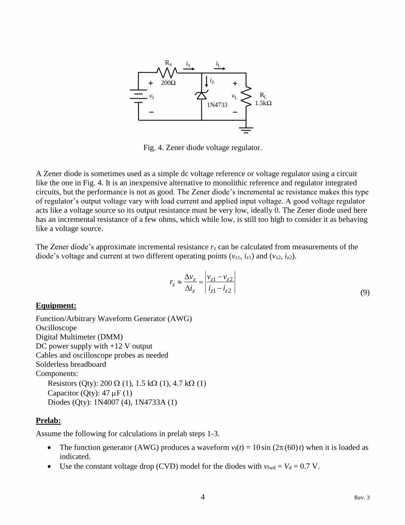
4 Rev. 3
A Zener diode is sometimes used as a simple dc voltage reference or voltage regulator using a circuit
like the one in Fig. 4. It is an inexpensive alternative to monolithic reference and regulator integrated
circuits, but the performance is not as good. The Zener diode’s incremental ac resistance makes this type
of regulator’s output voltage vary with load current and applied input voltage. A good voltage regulator
acts like a voltage source so its output resistance must be very low, ideally 0. The Zener diode used here
has an incremental resistance of a few ohms, which while low, is still too high to consider it as behaving
like a voltage source.
The Zener diode’s approximate incremental resistance rz can be calculated from measurements of the
diode’s voltage and current at two different operating points (vz1, iz1) and (vz2, iz2).
1 2
1 2
z z zz
z z z
v v vr
i i i
− = −
(9)
Equipment:
Function/Arbitrary Waveform Generator (AWG)
Oscilloscope
Digital Multimeter (DMM)
DC power supply with +12 V output
Cables and oscilloscope probes as needed
Solderless breadboard
Components:
Resistors (Qty): 200 (1), 1.5 k (1), 4.7 k (1)
Capacitor (Qty): 47 F (1)
Diodes (Qty): 1N4007 (4), 1N4733A (1)
Prelab:
Assume the following for calculations in prelab steps 1-3.
• The function generator (AWG) produces a waveform vI(t) = 10 sin (2 (60) t) when it is loaded as
indicated.
• Use the constant voltage drop (CVD) model for the diodes with vfwd = Vd = 0.7 V.
Fig. 4. Zener diode voltage regulator.
RL
1.5kΩ
RS
200Ω
1N4733
iS iL
iZ
vI
+
−
+
−
vL

5 Rev. 3
1. Perform the following calculations for the half-wave rectifier in Fig. 1. Put your results in Table 1.
a. Determine vo,peak, 1, and 2, for the rectifier output waveform of Fig. 1b.
b. Calculate the average (dc) value of vo(t) using Eq. 2.
c. Calculate the conduction angle .
2. Perform the following calculations for the full-wave rectifier in Fig. 2. Put your results in Table 1.
a. Determine vo,peak, 1, and 2 for the rectifier output waveform of Fig. 2b.
b. Calculate the average (dc) value of vo(t) using Eq. 4.
c. Calculate the conduction angle .
3. Perform the following calculations for the full-wave rectifier with filter capacitor in Fig. 3. Put your
results in Table 1.
a. Determine the maximum value of vo(t), vo,peak.
b. Determine the peak-to-peak ripple voltage, vr, peak-peak.
c. Determine the approximate average value of vO(t). You do not have to use integration. Assume
the ripple waveform has an ideal sawtooth shape with each “tooth” being a right triangle having
amplitude vr peak-peak as in Fig. 3b.
d. Sketch a realistic output waveform including ripple and superimpose it on the unfiltered full-
wave rectifier output waveform. Label the maximum and minimum output voltages, not just the
peak-peak value.
4. Perform the following calculations for the Zener-diode voltage regulator in Fig. 4. Use the CVD
model for the diode in reverse bias assuming it has a constant voltage drop of 5.1 V. Put your results
in Table 2.
a. If vI = 8 V dc, determine iS, iL, iZ, and vRL, the power dissipated in RS and the power dissipated in
the Zener diode.
b. Repeat part (a) for vI = 12 V dc.
Procedure:
General Information
1. a. Some oscilloscope measurement functions refer to command sequences for the Agilent
(Keysight) DSO 5014A.
b. When using the oscilloscope for dc voltage measurements, use Hi Res or Average acquisition
mode and use the smallest V/div scale factor that keeps the trace on the screen.
c. The function generator referenced in the instructions is the Agilent (Keysight) 33220A. This
generator’s output waveform connector is floating (not connected to power system ground). This
enables it to be used as a floating sine wave source for a full-wave bridge rectifier.
Half-Wave Rectifier
2. Perform measurements of the half-wave rectifier circuit shown in Fig. 1 as follows.

6 Rev. 3
a. Construct the circuit shown in Fig. 1.
b. Set up the function generator.
• Select a 60 Hz, 20 Vp-p sine wave.
• Make sure the function generator is in High-Z mode.
• Enable the function generator output.
c. Set up the oscilloscope.
• Monitor the function generator output waveform on the oscilloscope Ch. 1 and the resistor
voltage on Ch. 2.
• Use DC coupling on both channels.
• Trigger on Ch. 1 using Auto mode.
• Display at least 2 periods and line up the channel ground references together so the
waveforms are superimposed.
d. Have the oscilloscope measure the peak (not peak-peak) values of the Ch. 1 and Ch. 2
waveforms and the average value and of the Ch. 2 waveform.
• Verify that the input waveform’s amplitude is 20 Vp-p.
• Have your instructor verify that the display is correct.
• Save a copy of the oscilloscope display.
• Determine the difference between the Ch. 1 and Ch. 2 peak amplitudes.
Amplitude difference between input and output:
Full-Wave Rectifier
3. Perform measurements of the full-wave rectifier circuit shown in Fig. 5 as follows.
a. Construct the circuit shown in Fig. 5.
Note: You cannot connect the function generator to ground in this circuit. It must “float”. If you
do the rectifier will not work.
Since oscilloscope connectors are connected to power line ground internally, that establishes
the circuit 0 V ground reference.
For function generators that are connected to ground internally, the full-wave rectifier circuit
can be configured for a floating load and the load voltage measured differentially.
b. Set up the function generator.
• Select a 60 Hz, 20 Vp-p sine wave.
• Make sure the function generator is in High-Z mode.
• Enable the function generator output.
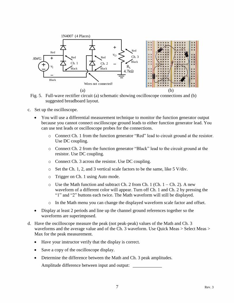
7 Rev. 3
c. Set up the oscilloscope.
• You will use a differential measurement technique to monitor the function generator output
because you cannot connect oscilloscope ground leads to either function generator lead. You
can use test leads or oscilloscope probes for the connections.
o Connect Ch. 1 from the function generator “Red” lead to circuit ground at the resistor.
Use DC coupling.
o Connect Ch. 2 from the function generator “Black” lead to the circuit ground at the
resistor. Use DC coupling.
o Connect Ch. 3 across the resistor. Use DC coupling.
o Set the Ch. 1, 2, and 3 vertical scale factors to be the same, like 5 V/div.
o Trigger on Ch. 1 using Auto mode.
o Use the Math function and subtract Ch. 2 from Ch. 1 (Ch. 1 − Ch. 2). A new
waveform of a different color will appear. Turn off Ch. 1 and Ch. 2 by pressing the
“1” and “2” buttons each twice. The Math waveform will still be displayed.
o In the Math menu you can change the displayed waveform scale factor and offset.
• Display at least 2 periods and line up the channel ground references together so the
waveforms are superimposed.
d. Have the oscilloscope measure the peak (not peak-peak) values of the Math and Ch. 3
waveforms and the average value and of the Ch. 3 waveform. Use Quick Meas > Select Meas >
Max for the peak measurement.
• Have your instructor verify that the display is correct.
• Save a copy of the oscilloscope display.
• Determine the difference between the Math and Ch. 3 peak amplitudes.
Amplitude difference between input and output:
(a) (b)
Fig. 5. Full-wave rectifier circuit (a) schematic showing oscilloscope connections and (b)
suggested breadboard layout.
+
−
vO
1N4007 (4 Places)
vI
+
−
Wires not connected!
Red
Black
AWG
RL
4.7kΩ
Red
Black
Red
Black
Ch. 1 Ch. 2
Red
Black
Ch. 3

8 Rev. 3
Filtered Full-Wave Rectifier
4. Perform measurements of the full-wave rectifier circuit with filter capacitor as follows.
a. The full-wave rectifier in Fig. 5 is modified by connecting a 47 F capacitor in parallel with the
load resistor.
• The capacitor is an electrolytic type and must be connected so the DC voltage has the right
polarity. Look at the capacitor case and you will see some “−” signs near one of the leads.
This lead must be connected to the low voltage side, in this case the circuit ground.
Note: Connecting an electrolytic capacitor backwards could damage it. If the current is high
enough it can fail catastrophically.
b. Disable or disconnect the function generator output (don’t turn the function generator off) and
connect the capacitor across the load resistor with the correct polarity.
c. Enable the function generator output and observe the Ch. 3 waveform. Because the ripple
amplitude is small, the output voltage is mostly dc. The average value of the Ch. 3 waveform
should be higher than it was in step 2.
Note: When the capacitor charges near the top of the rectified sine wave peaks, it acts like a low
impedance. The 50 internal impedance of the function generator will drop a significant
amount of the voltage. The result is distorted peaks in the Math waveform.
d. Save a copy of the display with the Ch. 3 and Math waveforms superimposed.
e. To measure the ripple waveform more carefully, change Ch. 3 to AC coupling. It will then center
the waveform at the Ch. 3 ground reference. Change the Ch. 3 scale factor so the ripple is
obvious. Have the oscilloscope measure the Ch. 3 peak-peak amplitude this time.
f. Save a copy of the display with just the Ch. 3 waveform displayed.
5. Perform measurements of the Zener diode voltage regulator circuit in Fig. 4 as follows.
a. Construct the circuit.
b. Use the +20 V output of the dc power supply. Set it to +8 V first.
c. Use the multimeter as a voltmeter and measure vL and vRS (the voltage across RS). Use these
values to calculate currents iS, iL, iZ. Enter the appropriate values in Table 2.
vL: vRS:
d. Calculate the power dissipated in RS and in the Zener diode and put the results in Table 2.
e. Set the power supply voltage to +12 V and repeat steps (c) and (d).
vL: vRS:
6. Results documentation summary.
a. You should have three oscilloscope screen shots, one each from steps 2, 3, and 4.
b. Be sure that you recorded data and calculated results in steps you were asked to.
e. Check with your instructor for additional documentation requirements.

9 Rev. 3
Analysis:
1. Consider the half-wave rectifier. Compare theoretical and measured results for the average and the
peak output voltages using percent error. Use the theoretical value as reference by subtracting it from
the measured value and dividing that result by the theoretical value; then convert to percent.
2. Consider the full-wave rectifier without filter capacitor. Compare theoretical and measured results
for the average and the peak output voltages using percent error.
3. Consider the full-wave rectifier with filter capacitor. Compare theoretical and measured results for
the average output voltage and the peak-peak ripple voltage using percent error.
4. Determine the approximate diode turn-on voltage from the half-wave rectifier waveforms.
5. How might the function generator’s internal impedance affect the filtered full-wave rectifier’s
average output voltage?
6. Consider the Zener diode voltage regulator. Use percent error to compare theoretical and measured
values of vL, iZ, and PZ at vI = 12 V.
7. Consider the Zener diode voltage regulator. Use data measured at vI = 8 V and 12 V to calculate the
diode on resistance rZ. Does the Zener diode voltage regulator act as a good voltage source (source
resistance less than 1 )?
Reference:
[1] A. Sedra and K. Smith, Microelectronic Circuits, 7ed., Oxford University Press, New York, 2015.

10 Rev. 3
Appendix:
Table 1. Calculated and measured rectifier data.
Rectifier
Prelab Calculations Experimental
vo,peak (V)
Conduction
Angle,
(degrees) Vavg (V) Vr,p-p (V) vo,peak (V) Vavg (V) Vr,p-p (V)
Half-wave
Full-wave
Filtered
full-wave
Table 2. Zener diode voltage regulator data.
Prelab Calculations Experimental
vI (V) iS
(mA) iZ
(mA) iL
(mA) vL (V)
PRS (mW)
PZ (mW)
iS (mA)
iZ (mA)
iL (mA)
vL (V)
PRS (mW)
PZ (mW)
8
12
Table 3. Errors between measured and calculated rectifier voltages.
Rectifier Peak Voltage Error (%) Avg. Voltage Error (%)
Peak-Peak Ripple
Voltage Error (%)
Half-wave
Full-wave
Filtered
full-wave

11 Rev. 3
Table 4. Errors between measured and calculated Zener diode circuit parameters at vI = 12 V.
Parameter Error (%)
Load voltage, vL
Zener diode current, iZ
Zener diode power, PZ
MOSFET Behavior
EE 3401 Laboratory Exercise
Electrical Engineering Department
Kennesaw State University
1 Rev. 4
Objectives:
You will study MOSFET behavior by measuring and analyzing NMOS transistor behavior in the
saturation region. MATLAB is used to fit curves to the measured data. In addition, simple logic circuits
using NMOS transistors are constructed and the transistor behavior in the ohmic region is observed.
Introduction:
The BS170 is designed for low-voltage, low-current switching applications such as power MOSFET
gate drivers. You will measure its dc transconductance curve ID vs. VGS and two common-source curves
in the saturation region. The ID vs. VGS curve for large MOSFETs like the BS170 is parabolic and Eq. 1
should be a close approximation. Using MATLAB, a parabolic equation is matched to the
transconductance curve and Vtn determined. MATLAB is also used to fit lines to the measured common-
source curves and values of channel-length modulation factor and drain-source resistance ro are found.
Transconductance gm at a fixed VDS is calculated.
( ) ( )2
12
nD GS tn DS GS tn
k WI V V V V V
L
= − +
(1)
Two simple logic circuits are built and their voltage input-output tables are measured. The rDS(on)
resistance of the transistors is also calculated.
Equipment:
Digital Multimeter (DMM)
DC power supply with +6 V and +20 V outputs
Cables as needed
Solderless breadboard
Components:
Resistors (Qty): 1 k (2)
MOSFET (Qty): BS170 (2)
Procedure:
General Information
1. Measurements like the ones in this lab exercise can result in too much power dissipation in the
transistor if you are not careful. The continuous power rating of the BS170 is 500 mW.
ID vs. VGS Measurements
2. Measure the BS170 ID vs. VGS transconductance characteristics for constant VDS using the circuit in
Fig. 1 as follows.
a. Construct the circuit in Fig. 1 using the +6V supply for VGS and the +20 V supply for VDS. Make
sure the supplies are set to 0 V before connecting them to the circuit.
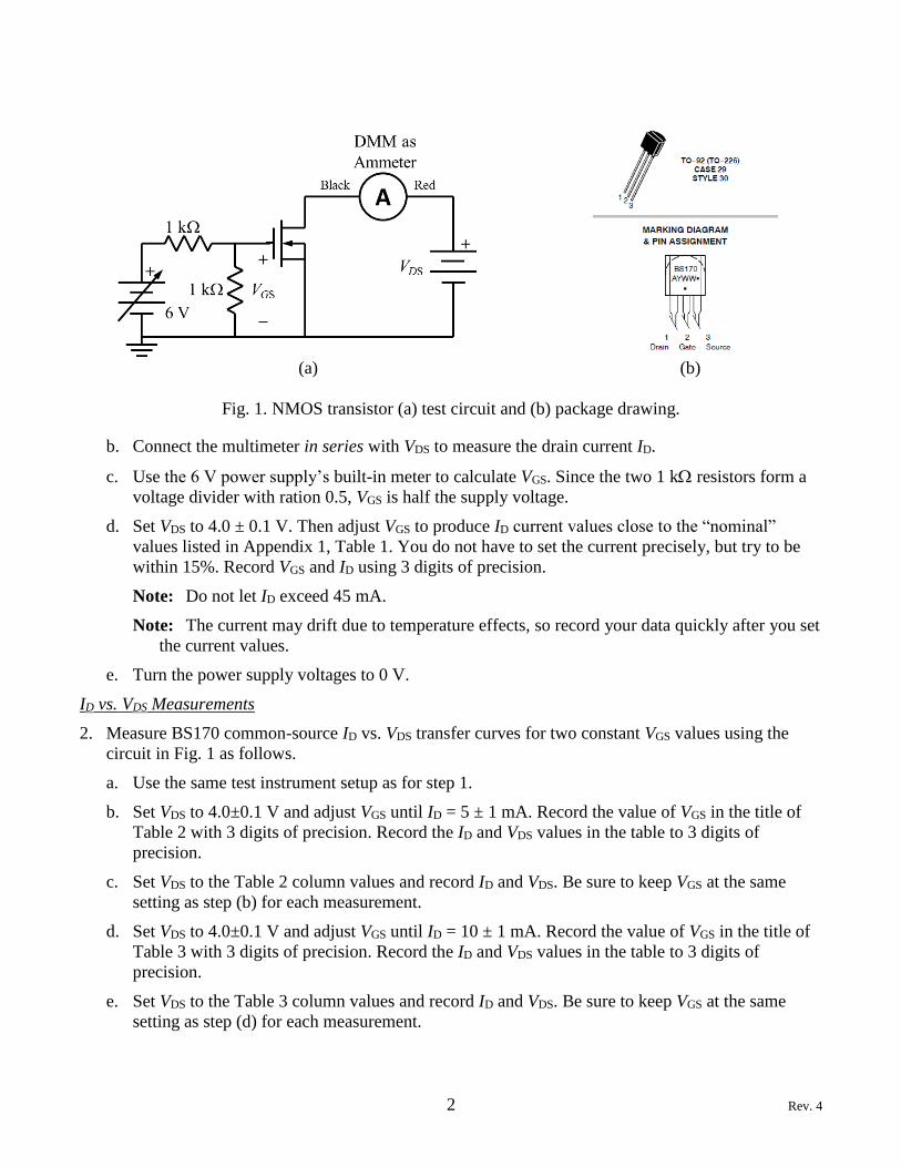
2 Rev. 4
b. Connect the multimeter in series with VDS to measure the drain current ID.
c. Use the 6 V power supply’s built-in meter to calculate VGS. Since the two 1 k resistors form a
voltage divider with ration 0.5, VGS is half the supply voltage.
d. Set VDS to 4.0 ± 0.1 V. Then adjust VGS to produce ID current values close to the “nominal”
values listed in Appendix 1, Table 1. You do not have to set the current precisely, but try to be
within 15%. Record VGS and ID using 3 digits of precision.
Note: Do not let ID exceed 45 mA.
Note: The current may drift due to temperature effects, so record your data quickly after you set
the current values.
e. Turn the power supply voltages to 0 V.
ID vs. VDS Measurements
2. Measure BS170 common-source ID vs. VDS transfer curves for two constant VGS values using the
circuit in Fig. 1 as follows.
a. Use the same test instrument setup as for step 1.
b. Set VDS to 4.0±0.1 V and adjust VGS until ID = 5 ± 1 mA. Record the value of VGS in the title of
Table 2 with 3 digits of precision. Record the ID and VDS values in the table to 3 digits of
precision.
c. Set VDS to the Table 2 column values and record ID and VDS. Be sure to keep VGS at the same
setting as step (b) for each measurement.
d. Set VDS to 4.0±0.1 V and adjust VGS until ID = 10 ± 1 mA. Record the value of VGS in the title of
Table 3 with 3 digits of precision. Record the ID and VDS values in the table to 3 digits of
precision.
e. Set VDS to the Table 3 column values and record ID and VDS. Be sure to keep VGS at the same
setting as step (d) for each measurement.
(a) (b)
Fig. 1. NMOS transistor (a) test circuit and (b) package drawing.
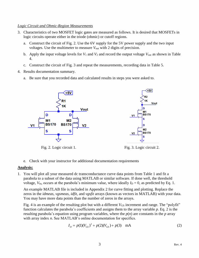
3 Rev. 4
Logic Circuit and Ohmic-Region Measurements
3. Characteristics of two MOSFET logic gates are measured as follows. It is desired that MOSFETs in
logic circuits operate either in the triode (ohmic) or cutoff regions.
a. Construct the circuit of Fig. 2. Use the 6V supply for the 5V power supply and the two input
voltages. Use the multimeter to measure Vout with 2 digits of precision.
b. Apply the input voltage levels for V1 and V2 and record the output voltage Vout as shown in Table
4.
c. Construct the circuit of Fig. 3 and repeat the measurements, recording data in Table 5.
4. Results documentation summary.
a. Be sure that you recorded data and calculated results in steps you were asked to.
e. Check with your instructor for additional documentation requirements
Analysis:
1. You will plot all your measured dc transconductance curve data points from Table 1 and fit a
parabola to a subset of the data using MATLAB or similar software. If done well, the threshold
voltage, Vtn, occurs at the parabola’s minimum value, where ideally ID = 0, as predicted by Eq. 1.
An example MATLAB file is included in Appendix 2 for curve fitting and plotting. Replace the
zeros in the idmeas, vgsmeas, idfit, and vgsfit arrays (known as vectors in MATLAB) with your data.
You may have more data points than the number of zeros in the arrays.
Fig. 4 is an example of the resulting plot but with a different VGS increment and range. The “polyfit”
function calculates the parabola’s coefficients and assigns them to the array variable p. Eq. 2 is the
resulting parabola’s equation using program variables, where the p(n) are constants in the p array
with array index n. See MATLAB’s online documentation for specifics.
2(1)( ) (2)( ) (3) mAD GS GSI p V p V p= + + (2)
Fig. 2. Logic circuit 1. Fig. 3. Logic circuit 2.
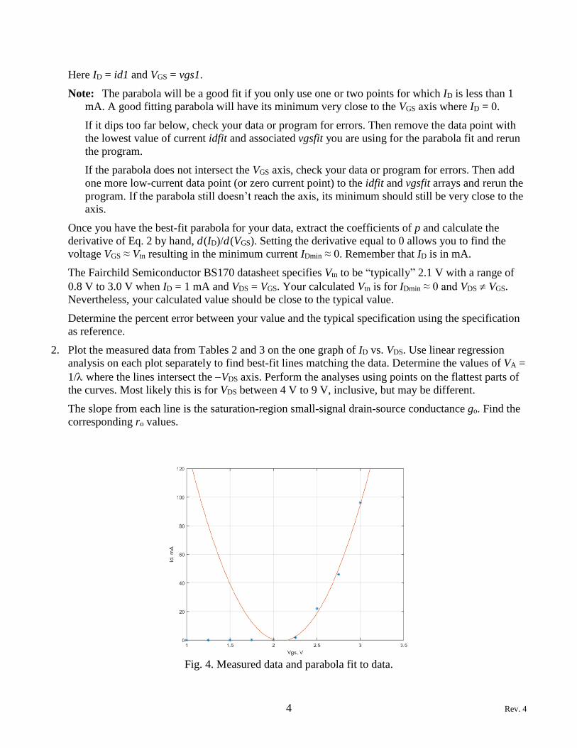
4 Rev. 4
Here ID = id1 and VGS = vgs1.
Note: The parabola will be a good fit if you only use one or two points for which ID is less than 1
mA. A good fitting parabola will have its minimum very close to the VGS axis where ID = 0.
If it dips too far below, check your data or program for errors. Then remove the data point with
the lowest value of current idfit and associated vgsfit you are using for the parabola fit and rerun
the program.
If the parabola does not intersect the VGS axis, check your data or program for errors. Then add
one more low-current data point (or zero current point) to the idfit and vgsfit arrays and rerun the
program. If the parabola still doesn’t reach the axis, its minimum should still be very close to the
axis.
Once you have the best-fit parabola for your data, extract the coefficients of p and calculate the
derivative of Eq. 2 by hand, d(ID)/d(VGS). Setting the derivative equal to 0 allows you to find the
voltage VGS ≈ Vtn resulting in the minimum current IDmin ≈ 0. Remember that ID is in mA.
The Fairchild Semiconductor BS170 datasheet specifies Vtn to be “typically” 2.1 V with a range of
0.8 V to 3.0 V when ID = 1 mA and VDS = VGS. Your calculated Vtn is for IDmin ≈ 0 and VDS VGS.
Nevertheless, your calculated value should be close to the typical value.
Determine the percent error between your value and the typical specification using the specification
as reference.
2. Plot the measured data from Tables 2 and 3 on the one graph of ID vs. VDS. Use linear regression
analysis on each plot separately to find best-fit lines matching the data. Determine the values of VA =
1/ where the lines intersect the −VDS axis. Perform the analyses using points on the flattest parts of
the curves. Most likely this is for VDS between 4 V to 9 V, inclusive, but may be different.
The slope from each line is the saturation-region small-signal drain-source conductance go. Find the
corresponding ro values.
Fig. 4. Measured data and parabola fit to data.

5 Rev. 4
You can use a similar program as the one used for question 1 with polyfit matching a first order
polynomial (line) to the data subset. If you use that program, remember that ID is in mA.
3. The derivative you calculated in question 1 is an expression of the transistor’s transconductance gm
as a function of VGS. Calculate gm at VGS = 2.6 V and VGS = 2.8 V in mA/V (or mS).
4. Determine the logic functions of the circuits in Figs. 2 and 3 from their input/output tables. Assume
output voltages above 2.5 V are logic 1 and those below 2.5 V are logic 0.
5. Calculate the on resistance rDS of each BS170 from data in Table 4, rows 2 and 3 using the VDS
values you measured.
6. Why is Vout in Table 4, row 4 less than Vout of either row 2 or 3?

6 Rev. 4
Appendix 1: Data Tables
Table 1. ID vs. VGS, VDS=4V
Important: Do Not Let ID Exceed 45 mA
Nominal ID (mA)
Parameter 0.1 0.2 0.4 0.7 1 2 4 7 10 20 40
Measured
ID (mA)
Measured
VGS (volts)
Table 2. ID vs. VDS, VGS=
Nominal VDS (V)
Parameter 1.0 2.0 3.0 4.0 5.0 6.0 7.0 8.0 9.0
Measured
VDS (V)
Measured
ID (mA)
Table 3. ID vs. VDS, VGS=
Nominal VDS (V)
Parameter 1.0 2.0 3.0 4.0 5.0 6.0 7.0 8.0 9.0
Measured
VDS (V)
Measured
ID (mA)

7 Rev. 4
Table 4. Logic circuit 1 Measurements.
V1 (V) V2 (V) Vout (V)
0 0
0 5
5 0
5 5
Table 5. Logic circuit 2 Measurements.
V1 (V) V2 (V) Vout (V)
0 0
0 5
5 0
5 5

8 Rev. 4
Appendix 2: MATLAB Parabola Matching Code Example
% MOSFET Parabola Matching
%
% The parabola match will be best if you include only one or two points
% with current less than 1 mA.
% Current values are in mA.
% Replace the zeros with your data. You may have a different number of
% points than the number of zeros.
%
idmeas=[0 0 0 0 0]; %All measured id values in mA
vgsmeas=[0 0 0 0 0]; %All measured vgs values
idfit=[0 0 0 0]; %Measured id values used for curve fit
vgsfit=[0 0 0 0]; %Measured vgs values used for curve fit
p=polyfit(vgsfit,idfit,2); %Find 2nd order polynomial coefficients
vgs1=[0:0.02:3.5]; %vgs range for parabola calculation, increment=0.02V
id1=polyval(p,vgs1);
plot(vgsmeas,idmeas,'*',vgs1,id1) %Points only for meas, line for calc
axis([1 3.5 0 120]) %Typical axis settings, you can change
xlabel('Vgs, V')
ylabel('Id, mA')
grid
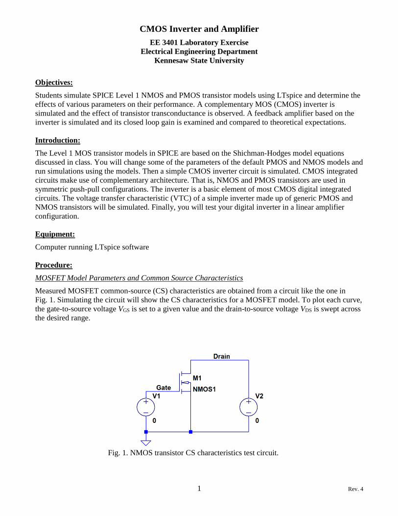
CMOS Inverter and Amplifier
EE 3401 Laboratory Exercise
Electrical Engineering Department
Kennesaw State University
1 Rev. 4
Objectives:
Students simulate SPICE Level 1 NMOS and PMOS transistor models using LTspice and determine the
effects of various parameters on their performance. A complementary MOS (CMOS) inverter is
simulated and the effect of transistor transconductance is observed. A feedback amplifier based on the
inverter is simulated and its closed loop gain is examined and compared to theoretical expectations.
Introduction:
The Level 1 MOS transistor models in SPICE are based on the Shichman-Hodges model equations
discussed in class. You will change some of the parameters of the default PMOS and NMOS models and
run simulations using the models. Then a simple CMOS inverter circuit is simulated. CMOS integrated
circuits make use of complementary architecture. That is, NMOS and PMOS transistors are used in
symmetric push-pull configurations. The inverter is a basic element of most CMOS digital integrated
circuits. The voltage transfer characteristic (VTC) of a simple inverter made up of generic PMOS and
NMOS transistors will be simulated. Finally, you will test your digital inverter in a linear amplifier
configuration.
Equipment:
Computer running LTspice software
Procedure:
MOSFET Model Parameters and Common Source Characteristics
Measured MOSFET common-source (CS) characteristics are obtained from a circuit like the one in
Fig. 1. Simulating the circuit will show the CS characteristics for a MOSFET model. To plot each curve,
the gate-to-source voltage VGS is set to a given value and the drain-to-source voltage VDS is swept across
the desired range.
Fig. 1. NMOS transistor CS characteristics test circuit.

2 Rev. 4
1. Prepare a NMOS transistor model.
a. Calculate the parameters of a NMOS transistor model that is based on the default model but with
following non-default parameters:
• Specify a k (KP) value calculated from the 3µm channel length process parameters given in
Table 1 in Appendix 1 using Eq. 1 below.
2A/Vn ox
n n oxox
k k Ct
= = = (1)
Where ox = 3.4510-11 F/m, n=710-2 m2/(Vs) and tox = 410-8 m.
• Specify a channel width of 180 µm, a channel length of 6 µm, a zero-bias threshold voltage
of Vt0 = 1Vand a channel length modulation factor of 0.01V-1.
• Give the model the name NMOS1.
b. The model statement is shown below with question marks for the values you need to provide.
Enter the model statement using the “.op” SPICE Directive toolbar button or Right
Click>Draft>SPICE Directive.
.model NMOS1 NMOS(KP=? VTO=? W=? L=? LAMBDA=?)
Note: SPICE uses W and L dimensions in meters and the “O” in VTO is not “zero”. Also,
SPICE does not use case-sensitive model names and parameters.
2. Use the LTspice DC Sweep analysis type to plot the common-source characteristics of the NMOS1
transistor model.
a. Create an LTspice schematic of the circuit in Fig. 1.
• Select the “nmos” component for the transistor. When you place the transistor, the model will
be specified as the default “NMOS”. Change it to a custom model NMOS1 by right clicking
on “NMOS” and changing it.
• Be sure to label the drain and gate nodes so their data will be easy to find after the simulation
is finished.
• Set the DC voltage values “V” of each source to 0. It doesn’t matter what values they are
since the DC Sweep analysis will use the voltage ranges you specify for the simulation.
b. Set up a nested DC sweep analysis that will sweep the drain-source voltage linearly from 0 to
16 V in 20 mV steps and sweeps the gate-source voltage linearly from 0 to 6 V in 500 mV steps.
• In the DC Sweep analysis setup, click on the 1st Source tab. Enter the following parameters:
Name of 1st Source to sweep: V2
Type of sweep: Linear
Start value: 0
Stop value: 16
Increment: 20e-3

3 Rev. 4
• Click on the 2nd Source tab. Enter the following parameters:
Name of 2nd Source to sweep: V1
Type of sweep: Linear
Start value: 0
Stop value: 6
Increment: 500e-3
c. Run the simulation.
d. Use the Waveform Viewer to display the drain current.
• The Waveform Viewer will display all the CS characteristic curves on one plot.
• Place a cursor at the quiescent point (Q-point) specified by VDS = 5 V and VGS = 3.5 V, and
use the ID value there to estimate the dc transconductance GM where
D
MGS
IG
V= (2)
Use the up/down arrows to step the cursor to a different curve. The cursor box will tell you
the VDS and ID value but not VGS. To be sure you are on the right VGS curve, right click on the
cursor itself and a box will open that tells you.
• Record the Q-point values for VDS, VGS, and ID, as well as GM in the NMOS1 row of Table 2
in Appendix 2.
• Save a copy of the NMOS1 transistor’s CS characteristics.
• Save a copy of the schematic.
e. Use the two cursors to estimate the transistor drain-to-source output resistance, ro VDS/ID at
the quiescent point in part (d).
• Put both cursors on the VGS = 3.5 V curve, one on either side of the Q-point. Use VDS values
of 4 V and 6 V for the cursor positions. The cursor box will tell you the slope go = ID/VDS.
• Record go and ro in Table 2.
3. Repeat step 2 for a PMOS transistor model. You will have to redraw the circuit so V1’s polarity is
+VSG and V2’s polarity is +VSD. Make sure the transistor’s source terminal is connected to ground.
See Fig. 3.
a. Create the PMOS1 model.
• The PMOS transistor has µp = 3.510-2 m2/(Vs), half the value of µn. Recalculate k for the
PMOS transistor. All other model parameters are the same, except Vt0 should be negative,
that is Vt0 = -1.
• Create a new model called PMOS1 with these parameters.
b. Run the simulation and plot −ID instead of ID.
• Calculate the parameters GM and ro of the PMOS1 model at VDS = −5 V and VGS = −3.5 V,
and NMOS1 models.
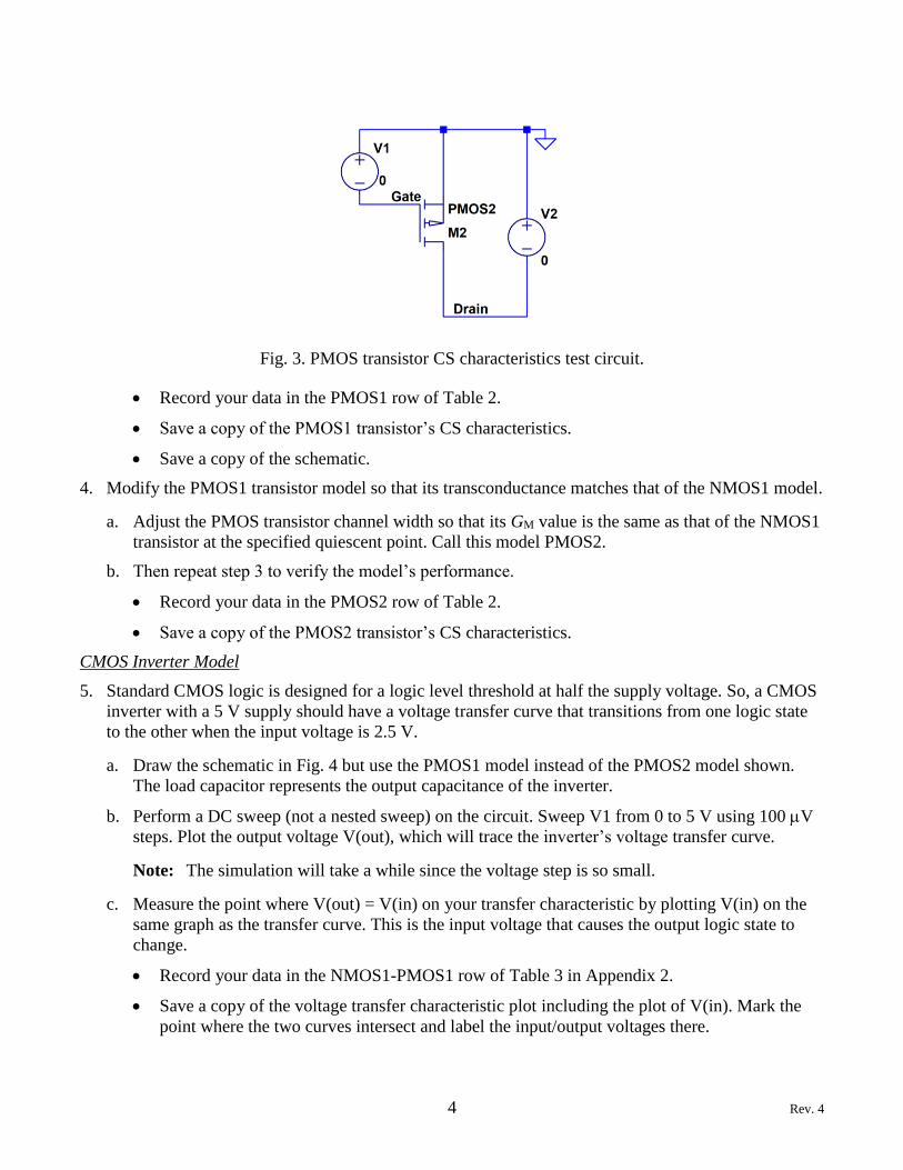
4 Rev. 4
• Record your data in the PMOS1 row of Table 2.
• Save a copy of the PMOS1 transistor’s CS characteristics.
• Save a copy of the schematic.
4. Modify the PMOS1 transistor model so that its transconductance matches that of the NMOS1 model.
a. Adjust the PMOS transistor channel width so that its GM value is the same as that of the NMOS1
transistor at the specified quiescent point. Call this model PMOS2.
b. Then repeat step 3 to verify the model’s performance.
• Record your data in the PMOS2 row of Table 2.
• Save a copy of the PMOS2 transistor’s CS characteristics.
CMOS Inverter Model
5. Standard CMOS logic is designed for a logic level threshold at half the supply voltage. So, a CMOS
inverter with a 5 V supply should have a voltage transfer curve that transitions from one logic state
to the other when the input voltage is 2.5 V.
a. Draw the schematic in Fig. 4 but use the PMOS1 model instead of the PMOS2 model shown.
The load capacitor represents the output capacitance of the inverter.
b. Perform a DC sweep (not a nested sweep) on the circuit. Sweep V1 from 0 to 5 V using 100 V
steps. Plot the output voltage V(out), which will trace the inverter’s voltage transfer curve.
Note: The simulation will take a while since the voltage step is so small.
c. Measure the point where V(out) = V(in) on your transfer characteristic by plotting V(in) on the
same graph as the transfer curve. This is the input voltage that causes the output logic state to
change.
• Record your data in the NMOS1-PMOS1 row of Table 3 in Appendix 2.
• Save a copy of the voltage transfer characteristic plot including the plot of V(in). Mark the
point where the two curves intersect and label the input/output voltages there.
Fig. 3. PMOS transistor CS characteristics test circuit.
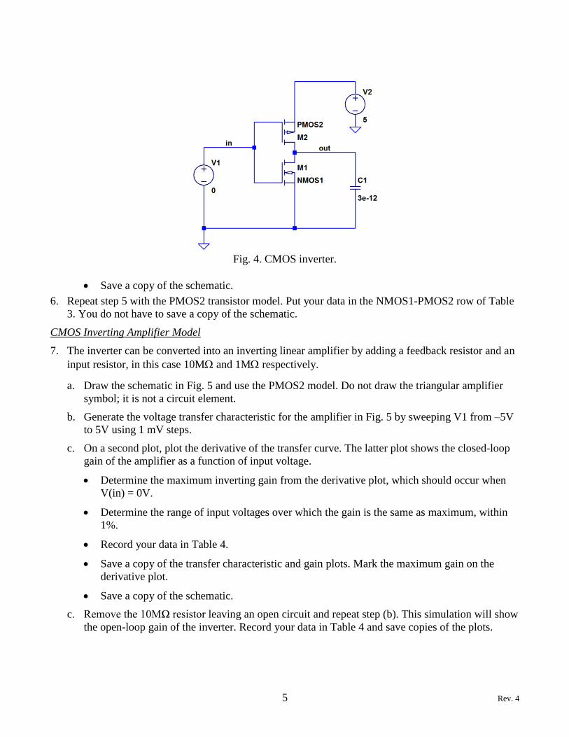
5 Rev. 4
• Save a copy of the schematic.
6. Repeat step 5 with the PMOS2 transistor model. Put your data in the NMOS1-PMOS2 row of Table
3. You do not have to save a copy of the schematic.
CMOS Inverting Amplifier Model
7. The inverter can be converted into an inverting linear amplifier by adding a feedback resistor and an
input resistor, in this case 10M and 1M respectively.
a. Draw the schematic in Fig. 5 and use the PMOS2 model. Do not draw the triangular amplifier
symbol; it is not a circuit element.
b. Generate the voltage transfer characteristic for the amplifier in Fig. 5 by sweeping V1 from –5V
to 5V using 1 mV steps.
c. On a second plot, plot the derivative of the transfer curve. The latter plot shows the closed-loop
gain of the amplifier as a function of input voltage.
• Determine the maximum inverting gain from the derivative plot, which should occur when
V(in) = 0V.
• Determine the range of input voltages over which the gain is the same as maximum, within
1%.
• Record your data in Table 4.
• Save a copy of the transfer characteristic and gain plots. Mark the maximum gain on the
derivative plot.
• Save a copy of the schematic.
c. Remove the 10MΩ resistor leaving an open circuit and repeat step (b). This simulation will show
the open-loop gain of the inverter. Record your data in Table 4 and save copies of the plots.
Fig. 4. CMOS inverter.
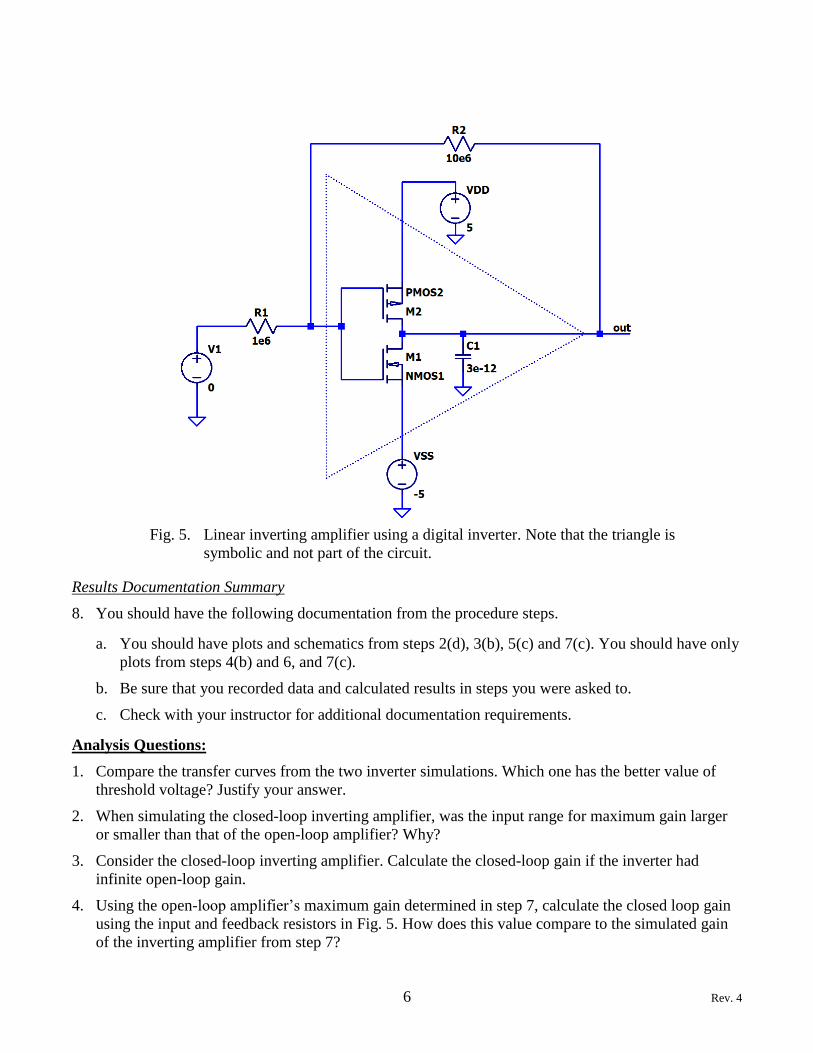
6 Rev. 4
Results Documentation Summary
8. You should have the following documentation from the procedure steps.
a. You should have plots and schematics from steps 2(d), 3(b), 5(c) and 7(c). You should have only
plots from steps 4(b) and 6, and 7(c).
b. Be sure that you recorded data and calculated results in steps you were asked to.
c. Check with your instructor for additional documentation requirements.
Analysis Questions:
1. Compare the transfer curves from the two inverter simulations. Which one has the better value of
threshold voltage? Justify your answer.
2. When simulating the closed-loop inverting amplifier, was the input range for maximum gain larger
or smaller than that of the open-loop amplifier? Why?
3. Consider the closed-loop inverting amplifier. Calculate the closed-loop gain if the inverter had
infinite open-loop gain.
4. Using the open-loop amplifier’s maximum gain determined in step 7, calculate the closed loop gain
using the input and feedback resistors in Fig. 5. How does this value compare to the simulated gain
of the inverting amplifier from step 7?
Fig. 5. Linear inverting amplifier using a digital inverter. Note that the triangle is
symbolic and not part of the circuit.

7 Rev. 4
Appendix 1: Typical MOSFET Process Parameters
Table 1. Typical process parameters for 3µm minimum allowed channel length [1].
Reference:
[1] P. Gray, P. Hurst, S. Lewis, R. Meyer, Analysis and Design of Analog Integrated Circuits, 5ed,
New York, John Wiley and Sons, 2009.
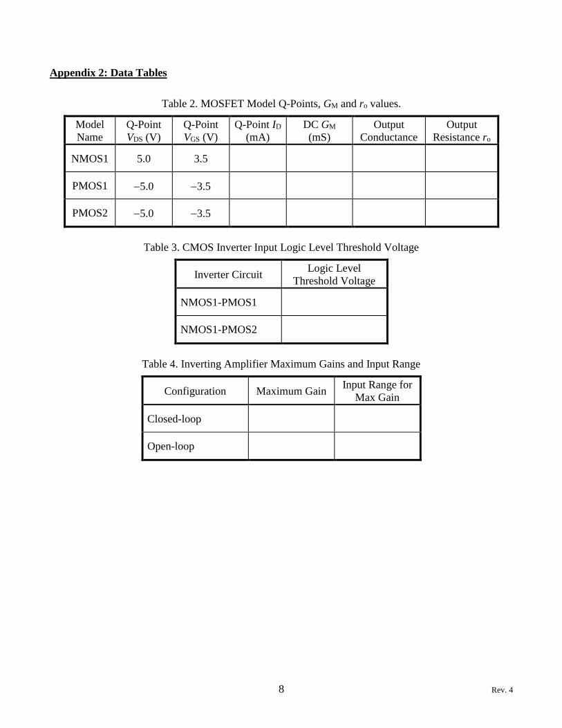
8 Rev. 4
Appendix 2: Data Tables
Table 2. MOSFET Model Q-Points, GM and ro values.
Model
Name
Q-Point
VDS (V)
Q-Point
VGS (V)
Q-Point ID
(mA)
DC GM
(mS)
Output
Conductance
Output
Resistance ro
NMOS1 5.0 3.5
PMOS1 −5.0 −3.5
PMOS2 −5.0 −3.5
Table 3. CMOS Inverter Input Logic Level Threshold Voltage
Inverter Circuit Logic Level
Threshold Voltage
NMOS1-PMOS1
NMOS1-PMOS2
Table 4. Inverting Amplifier Maximum Gains and Input Range
Configuration Maximum Gain Input Range for
Max Gain
Closed-loop
Open-loop
BJT DC Characteristics
EE 3401 Laboratory Exercise
Electrical Engineering Department
Kennesaw State University
1 Rev. 4
Objectives:
Students measure the common-emitter output characteristics of a NPN transistor and derive
transistor parameters from the data. A diode-connected configuration is also examined.
MATLAB is used to fit curves to measured data.
Introduction:
The 2N2222 is a popular NPN small-signal transistor. It is a general-purpose transistor with good
bandwidth, current gain and switching characteristics. It comes in two popular packages, the
metal TO-18 and the plastic TO-92. Figs. 1 and 2 show the packages and lead configurations. The
two versions have slightly different specifications.
The first part of the procedure involves measuring the transistor’s output characteristics in a
common-emitter configuration for two different base currents. Linear regression analyses are
performed on data for each base current using MATLAB. Transistor parameters , , gm, ro and
VA are obtained.
In the second part of the procedure, characteristics of a diode-connected configuration are
measured. This configuration is used in current mirrors because the transistor is always in the
active region and it has very low VCE variation over a broad range of collector current. MATLAB
is used to plot the output resistance of the configuration.
Equipment:
One or two digital multimeters (DMM)
Oscilloscope
Triple output power supply
Cables and oscilloscope probes as needed
Solderless breadboard
Fig. 1. TO-18 case version. Note that the case
is connected to the collector lead. The tab is
closest to the emitter.
Fig. 2. TO-92 case version.
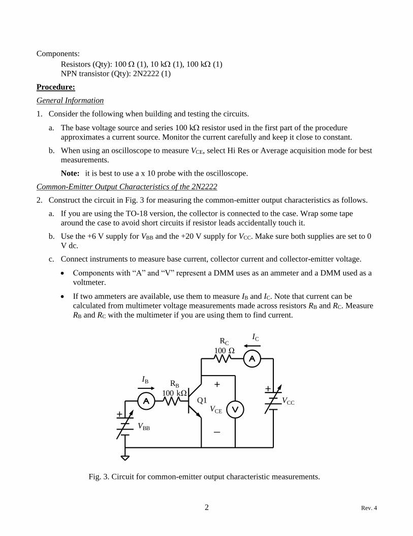
2 Rev. 4
Components:
Resistors (Qty): 100 (1), 10 k (1), 100 k (1)
NPN transistor (Qty): 2N2222 (1)
Procedure:
General Information
1. Consider the following when building and testing the circuits.
a. The base voltage source and series 100 k resistor used in the first part of the procedure
approximates a current source. Monitor the current carefully and keep it close to constant.
b. When using an oscilloscope to measure VCE, select Hi Res or Average acquisition mode for best
measurements.
Note: it is best to use a x 10 probe with the oscilloscope.
Common-Emitter Output Characteristics of the 2N2222
2. Construct the circuit in Fig. 3 for measuring the common-emitter output characteristics as follows.
a. If you are using the TO-18 version, the collector is connected to the case. Wrap some tape
around the case to avoid short circuits if resistor leads accidentally touch it.
b. Use the +6 V supply for VBB and the +20 V supply for VCC. Make sure both supplies are set to 0
V dc.
c. Connect instruments to measure base current, collector current and collector-emitter voltage.
• Components with “A” and “V” represent a DMM uses as an ammeter and a DMM used as a
voltmeter.
• If two ammeters are available, use them to measure IB and IC. Note that current can be
calculated from multimeter voltage measurements made across resistors RB and RC. Measure
RB and RC with the multimeter if you are using them to find current.
Fig. 3. Circuit for common-emitter output characteristic measurements.
IC
RB
100 kΩ
RC
100 Ω
+
+
VBB
VCC
IB +
_
VCE
Q1

3 Rev. 4
RB value: RC value:
• Use the oscilloscope to measure VCE. Select Hi-Res or Average acquisition mode, Auto
triggering, 10 msec/div, and have the oscilloscope measure the Average value.
3. Make measurements as follows, using Tables 1 and 2 to record your data. Your measurements will
drift with temperature changes in the transistor, so record the data as soon as your voltage and
current adjustments are complete.
a. Adjust VCC to set VCE = 2 ± 0.1 V.
b. Adjust VBB to set IB = 20 μA ± 1 μA. Record the actual value in the title of Appendix 1, Table 1.
Check that VCE = 2 V and readjust VCE if necessary. Then verify that IB is still within tolerance.
Measure and record the value of IC and VCE in the table. Use 3 digits of precision.
Note: If measuring base current using the voltage across RB, calculate the expected voltage VRB
= IBRB using the measured RB value. Then adjust VBB to set that voltage.
Note: VCE VCC due to the voltage drop across RC.
c. Adjust VCC to set VCE = 4 ± 0.1 V. Measure and record the value of VCE and IC.
d. Repeat procedure step 3(c) for VCE = 6 V, 8 V, 10 V, 12 V and 14 V.
e. Adjust VCC to return VCE to 2 ± 0.1 Vdc. Then adjust VBB to set IB = 40 μA ± 1 μA. Record the
actual value of IB in the title of Table 2. Use 3 digits of precision.
f. Repeat procedure steps 3(c) and 3(d) for the new value of IB.
Diode-Connected Transistor Circuit
4. Modify the circuit as shown in Fig. 4 to measure the characteristics of a diode-connected transistor
as described below. Your measurements will drift with temperature changes in the transistor, so
record the data as soon as your voltage and current adjustments are complete.
a. Use the +20 V supply for VCC as before. Make sure the supply is set to 0 V dc.
b. Replace RC with a 10 kΩ resistor.
c. Connect instruments to measure IE and VCE.
• You must use the multimeter to measure VCE accurately.
• IE can be calculated from a multimeter voltage measurement made across RC. If you are
calculating IE, measure RC with the multimeter to find its actual resistance and use it in the
calculation.
RC value:
Note: The current through RC is IE = IC + IB for this transistor configuration.
5. Make measurements as follows, using Table 3 to record your data.
a. Adjust VCC to set IE = 250 μA ± 2%. Record the actual value or IE. Measure VCE with the
multimeter and record the value. Use 3 digits of precision.
b. Adjust VCC to set IE = 500 μA ± 2%. Record IE and VCE.
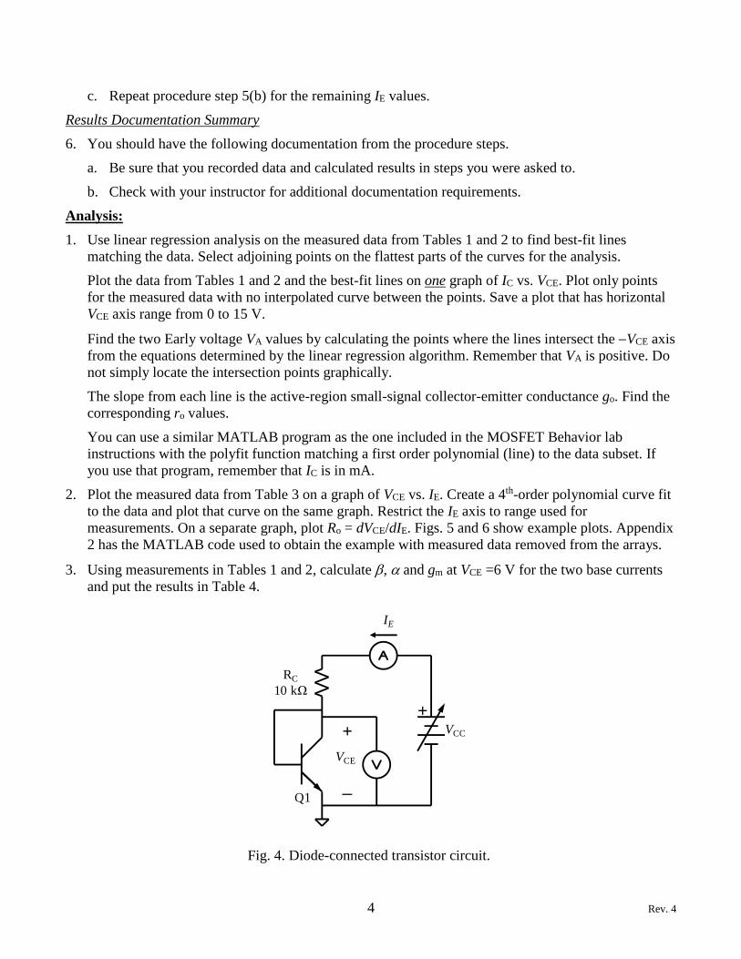
4 Rev. 4
c. Repeat procedure step 5(b) for the remaining IE values.
Results Documentation Summary
6. You should have the following documentation from the procedure steps.
a. Be sure that you recorded data and calculated results in steps you were asked to.
b. Check with your instructor for additional documentation requirements.
Analysis:
1. Use linear regression analysis on the measured data from Tables 1 and 2 to find best-fit lines
matching the data. Select adjoining points on the flattest parts of the curves for the analysis.
Plot the data from Tables 1 and 2 and the best-fit lines on one graph of IC vs. VCE. Plot only points
for the measured data with no interpolated curve between the points. Save a plot that has horizontal
VCE axis range from 0 to 15 V.
Find the two Early voltage VA values by calculating the points where the lines intersect the −VCE axis
from the equations determined by the linear regression algorithm. Remember that VA is positive. Do
not simply locate the intersection points graphically.
The slope from each line is the active-region small-signal collector-emitter conductance go. Find the
corresponding ro values.
You can use a similar MATLAB program as the one included in the MOSFET Behavior lab
instructions with the polyfit function matching a first order polynomial (line) to the data subset. If
you use that program, remember that IC is in mA.
2. Plot the measured data from Table 3 on a graph of VCE vs. IE. Create a 4th-order polynomial curve fit
to the data and plot that curve on the same graph. Restrict the IE axis to range used for
measurements. On a separate graph, plot Ro = dVCE/dIE. Figs. 5 and 6 show example plots. Appendix
2 has the MATLAB code used to obtain the example with measured data removed from the arrays.
3. Using measurements in Tables 1 and 2, calculate , and gm at VCE =6 V for the two base currents
and put the results in Table 4.
Fig. 4. Diode-connected transistor circuit.
IE
RC
10 kΩ
+VCC+
_
VCE
Q1
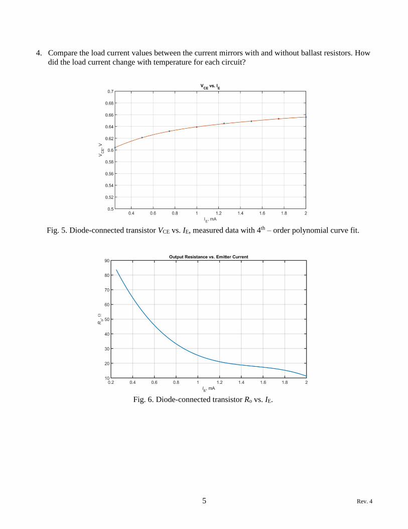
5 Rev. 4
4. Compare the load current values between the current mirrors with and without ballast resistors. How
did the load current change with temperature for each circuit?
Fig. 5. Diode-connected transistor VCE vs. IE, measured data with 4th – order polynomial curve fit.
Fig. 6. Diode-connected transistor Ro vs. IE.

6 Rev. 4
Appendix 1: Data Tables
Table 1. IC vs. VCE, IB = ___________
Nominal VCE (V)
Parameter 2.0 4.0 6.0 8.0 10.0 12.0 14.0
Measured
VCE (V)
Measured
IC (mA)
Table 2. IC vs. VCE, IB = ___________
Nominal VCE (V)
Parameter 2.0 4.0 6.0 8.0 10.0 12.0 14.0
Measured
VCE (V)
Measured
IC (mA)
Table 3. Diode-Connected Transistor Output Characteristics VCE vs. IE.
Nominal IE (mA)
Parameter 0.25 0.50 0.75 1.0 1.25 1.50 1.75 2.0
Measured
IE (mA)
Measured
VCE (V)
Table 4. Calculated Transistor Parameters at VCE = 6 V.
Nominal IB (A) gm
20
40

7 Rev. 4
Appendix 2: MATLAB Code for Diode-Connected Transistor Plots
% Diodeconn.m
% BJT diode connected transistor Vce vs. Ie data and curve fit.
%
% Current values are in mA.
%
% The figure(2) graph shows how to specify italic and subscript text in labels.
%
IeMeas=[0 0 0 0 0 0 0 0]; %Measured Ie
VceMeas=[ 0 0 0 0 0 0 0 0]; %Measured Vce
Ie=polyfit(IeMeas,VceMeas,4); % 4th-order polynomial fit
IeRange=[0.25:0.002:2]; % Ie range in mA
VceFit=polyval(Ie,IeRange); % Make smooth curve over measured Ie range
% dIe is derivative of Ie polynomial found manually from Ie coefficients
dIe=[ 0 0 0 0 ]; % Derivative of Ie polynomial, 4 terms
% Ro is output resistance curve from 4th order polynomial fit
Ro=polyval(dIe,IeRange)*1000;
figure(1)
plot(IeMeas,VceMeas,'*',IeRange,VceFit)
axis([0.25 2 0.5 0.7])
title('V_CE vs. I_E')
xlabel('I_E, mA')
ylabel('V_CE, V')
grid
figure(2) % Use separate figure
plot(IeRange,Ro)
title('Output Resistance vs. Emitter Current')
xlabel('\itI\rm_E, mA')
ylabel('\itR\rm_o, \Omega')
grid

BJT Amplifiers
EE 3401 Laboratory Exercise
Electrical Engineering Department
Kennesaw State University
1 Rev. 2
Objectives:
You will analyze, build and test NPN transistor amplifiers in order see how they perform. Three
common-emitter (CE) amplifiers and one common collector (CC) amplifier are examined. The effect of
an emitter resistor on the quality of the bias circuit and the amplifier gain are observed.
Introduction:
The CE amplifier in Fig. 1 has no emitter degeneration resistor. The resulting dc bias circuit quiescent
point (Q-point) that is sensitive to variation. However, it has high ac voltage gain. The function
generator’s signal is connected to the base through a dc blocking capacitor. The second CE amplifier in
Fig. 2 has an emitter resistor, which makes the Q-point much less sensitive to variation. But, the gain
is much lower than that of the first circuit. The third circuit uses a capacitor to “bypass” the emitter
resistor for ac signals, increasing the gain. The capacitor does not affect the dc bias circuit, so the Q-
point is the same as for the second circuit.
The common-collector amplifier in Fig. 4 is a modification of the Fig. 2 circuit with the collector
resistor removed.
Equipment:
Function/Arbitrary Waveform Generator
Oscilloscope
Digital Multimeter (DMM)
DC power supply with +20 V output
Cables and oscilloscope probes as needed
Solderless breadboard
Components:
Resistors (Qty): 100 (3), 1 k (1), 56 k (1), 180 k (1)
Capacitors (Qty): 4.7 F (2)
NPN transistor (Qty): 2N2222 (1)
Prelab:
1. For the three amplifier circuits in Figs. 1, 2, 3, and 4:
a. Calculate the Q-point values of collector current (IC) and collector-emitter voltage (VCE). Assume
DC=150, VBE = 0.65 V, VCE(SAT) =0.2 V, and VA = . Put your results in the prelab columns of
Table 1.
b. Calculate the small-signal voltage gain Vout/Vin. Assume AC=150 and the capacitors are short
circuits. Put your results in the prelab columns of Table 2. Record the gain magnitude in column
2 and the phase shift in column 3. A non-inverting gain has a phase shift of 0 and an inverting
gain has a phase shift 180.
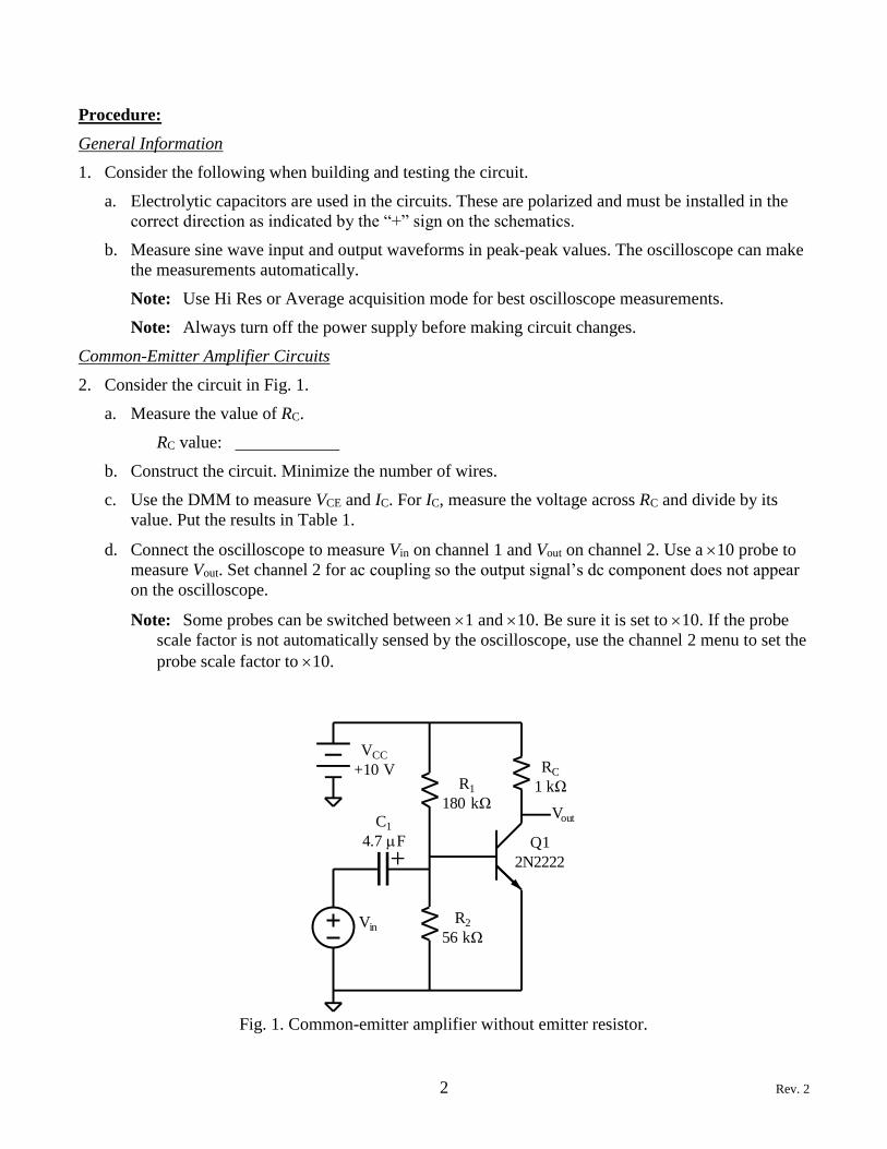
2 Rev. 2
Procedure:
General Information
1. Consider the following when building and testing the circuit.
a. Electrolytic capacitors are used in the circuits. These are polarized and must be installed in the
correct direction as indicated by the “+” sign on the schematics.
b. Measure sine wave input and output waveforms in peak-peak values. The oscilloscope can make
the measurements automatically.
Note: Use Hi Res or Average acquisition mode for best oscilloscope measurements.
Note: Always turn off the power supply before making circuit changes.
Common-Emitter Amplifier Circuits
2. Consider the circuit in Fig. 1.
a. Measure the value of RC.
RC value:
b. Construct the circuit. Minimize the number of wires.
c. Use the DMM to measure VCE and IC. For IC, measure the voltage across RC and divide by its
value. Put the results in Table 1.
d. Connect the oscilloscope to measure Vin on channel 1 and Vout on channel 2. Use a 10 probe to
measure Vout. Set channel 2 for ac coupling so the output signal’s dc component does not appear
on the oscilloscope.
Note: Some probes can be switched between 1 and 10. Be sure it is set to 10. If the probe
scale factor is not automatically sensed by the oscilloscope, use the channel 2 menu to set the
probe scale factor to 10.
Fig. 1. Common-emitter amplifier without emitter resistor.
Q1
2N2222
R1
180 kΩ
R2
56 kΩ
RC
1 kΩ
C1
4.7 F
VCC
+10 V
Vin
Vout
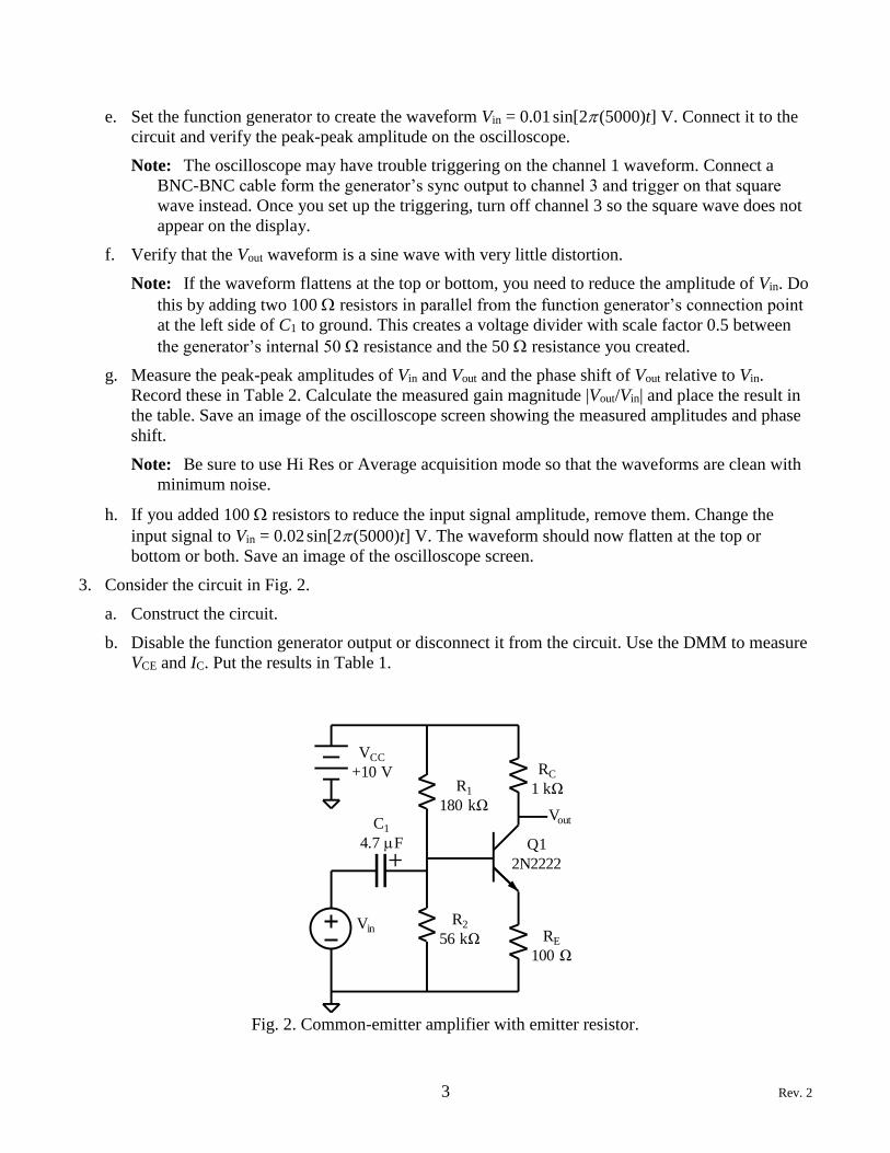
3 Rev. 2
e. Set the function generator to create the waveform Vin = 0.01 sin[2 (5000)t] V. Connect it to the
circuit and verify the peak-peak amplitude on the oscilloscope.
Note: The oscilloscope may have trouble triggering on the channel 1 waveform. Connect a
BNC-BNC cable form the generator’s sync output to channel 3 and trigger on that square
wave instead. Once you set up the triggering, turn off channel 3 so the square wave does not
appear on the display.
f. Verify that the Vout waveform is a sine wave with very little distortion.
Note: If the waveform flattens at the top or bottom, you need to reduce the amplitude of Vin. Do
this by adding two 100 resistors in parallel from the function generator’s connection point
at the left side of C1 to ground. This creates a voltage divider with scale factor 0.5 between
the generator’s internal 50 resistance and the 50 resistance you created.
g. Measure the peak-peak amplitudes of Vin and Vout and the phase shift of Vout relative to Vin.
Record these in Table 2. Calculate the measured gain magnitude |Vout/Vin| and place the result in
the table. Save an image of the oscilloscope screen showing the measured amplitudes and phase
shift.
Note: Be sure to use Hi Res or Average acquisition mode so that the waveforms are clean with
minimum noise.
h. If you added 100 resistors to reduce the input signal amplitude, remove them. Change the
input signal to Vin = 0.02sin[2 (5000)t] V. The waveform should now flatten at the top or
bottom or both. Save an image of the oscilloscope screen.
3. Consider the circuit in Fig. 2.
a. Construct the circuit.
b. Disable the function generator output or disconnect it from the circuit. Use the DMM to measure
VCE and IC. Put the results in Table 1.
Fig. 2. Common-emitter amplifier with emitter resistor.
Q1
2N2222
R1
180 kΩ
R2
56 kΩ
RC
1 kΩ
RE
100 Ω
C1
4.7 F
VCC
+10 V
Vin
Vout
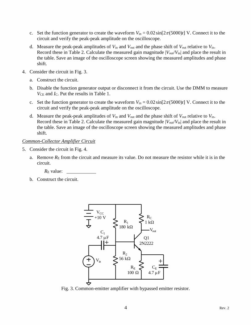
4 Rev. 2
c. Set the function generator to create the waveform Vin = 0.02 sin[2 (5000)t] V. Connect it to the
circuit and verify the peak-peak amplitude on the oscilloscope.
d. Measure the peak-peak amplitudes of Vin and Vout and the phase shift of Vout relative to Vin.
Record these in Table 2. Calculate the measured gain magnitude |Vout/Vin| and place the result in
the table. Save an image of the oscilloscope screen showing the measured amplitudes and phase
shift.
4. Consider the circuit in Fig. 3.
a. Construct the circuit.
b. Disable the function generator output or disconnect it from the circuit. Use the DMM to measure
VCE and IC. Put the results in Table 1.
c. Set the function generator to create the waveform Vin = 0.02 sin[2 (5000)t] V. Connect it to the
circuit and verify the peak-peak amplitude on the oscilloscope.
d. Measure the peak-peak amplitudes of Vin and Vout and the phase shift of Vout relative to Vin.
Record these in Table 2. Calculate the measured gain magnitude |Vout/Vin| and place the result in
the table. Save an image of the oscilloscope screen showing the measured amplitudes and phase
shift.
Common-Collector Amplifier Circuit
5. Consider the circuit in Fig. 4.
a. Remove RE from the circuit and measure its value. Do not measure the resistor while it is in the
circuit.
RE value:
b. Construct the circuit.
Fig. 3. Common-emitter amplifier with bypassed emitter resistor.
CE
4.7 F
Q1
2N2222
R1
180 kΩ
R2
56 kΩ
RC
1 kΩ
RE
100 Ω
C1
4.7 F
VCC
+10 V
Vin
Vout
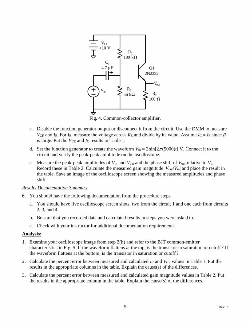
5 Rev. 2
c. Disable the function generator output or disconnect it from the circuit. Use the DMM to measure
VCE and IE. For IE, measure the voltage across RE and divide by its value. Assume IC IE since
is large. Put the VCE and IC results in Table 1.
d. Set the function generator to create the waveform Vin = 2 sin[2 (5000)t] V. Connect it to the
circuit and verify the peak-peak amplitude on the oscilloscope.
e. Measure the peak-peak amplitudes of Vin and Vout and the phase shift of Vout relative to Vin.
Record these in Table 2. Calculate the measured gain magnitude |Vout/Vin| and place the result in
the table. Save an image of the oscilloscope screen showing the measured amplitudes and phase
shift.
Results Documentation Summary
6. You should have the following documentation from the procedure steps.
a. You should have five oscilloscope screen shots, two from the circuit 1 and one each from circuits
2, 3, and 4.
b. Be sure that you recorded data and calculated results in steps you were asked to.
c. Check with your instructor for additional documentation requirements.
Analysis:
1. Examine your oscilloscope image from step 2(h) and refer to the BJT common-emitter
characteristics in Fig. 5. If the waveform flattens at the top, is the transistor in saturation or cutoff ? If
the waveform flattens at the bottom, is the transistor in saturation or cutoff ?
2. Calculate the percent error between measured and calculated IC and VCE values in Table 1. Put the
results in the appropriate columns in the table. Explain the cause(s) of the differences.
3. Calculate the percent error between measured and calculated gain magnitude values in Table 2. Put
the results in the appropriate column in the table. Explain the cause(s) of the differences.
Fig. 4. Common-collector amplifier.
Q1
2N2222
R1
180 kΩ
R2
56 kΩ RE
100 Ω
C1
4.7 F
Vin
VCC
+10 V
Vout
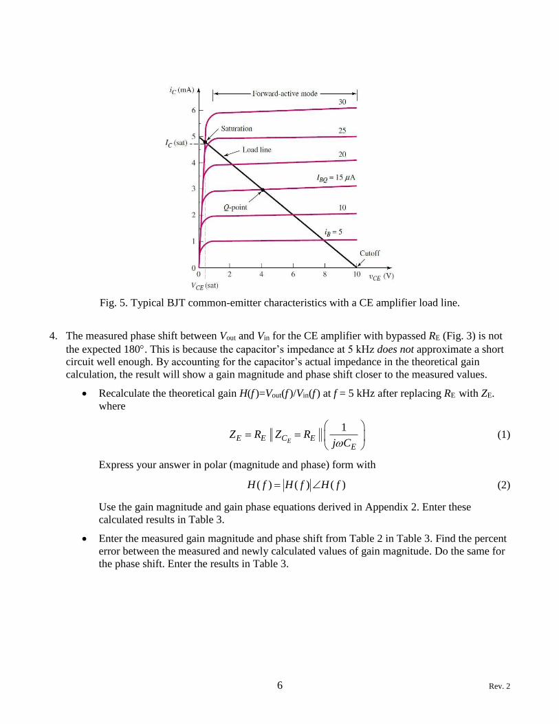
6 Rev. 2
4. The measured phase shift between Vout and Vin for the CE amplifier with bypassed RE (Fig. 3) is not
the expected 180. This is because the capacitor’s impedance at 5 kHz does not approximate a short
circuit well enough. By accounting for the capacitor’s actual impedance in the theoretical gain
calculation, the result will show a gain magnitude and phase shift closer to the measured values.
• Recalculate the theoretical gain H(f )=Vout(f )/Vin(f ) at f = 5 kHz after replacing RE with ZE.
where
1
EE E C EE
Z R Z Rj C
= =
(1)
Express your answer in polar (magnitude and phase) form with
( ) ( ) ( )H f H f H f= (2)
Use the gain magnitude and gain phase equations derived in Appendix 2. Enter these
calculated results in Table 3.
• Enter the measured gain magnitude and phase shift from Table 2 in Table 3. Find the percent
error between the measured and newly calculated values of gain magnitude. Do the same for
the phase shift. Enter the results in Table 3.
Fig. 5. Typical BJT common-emitter characteristics with a CE amplifier load line.

7 Rev. 2
Appendix 1: Data Tables
Table 1. Calculated and measured amplifier Q-point data.
Amplifier
Calculated
IC (mA)
(Prelab)
Calculated
VCE (V)
(Prelab)
Measured
IC (mA)
Measured
VCE (V)
IC
Percent
Error
VCE
Percent
Error
CE, no RE,
Fig. 1
CE, with RE,
Fig. 2
CE,
bypassed RE,
Fig. 3
CC, Fig. 4
Table 2. Calculated and measured amplifier gain data.
Amplifier
Calculated
Gain
Magnitude
|Vout/Vin|
(Prelab)
Calculated
Gain
Phase Shift
(Prelab)
Measured
Vin (V)
Measured
Vout (V)
Measured
Gain
Magnitude
|Vout/Vin|
Measured
Gain
Phase Shift
Gain
Magnitude
Percent
Error
CE, no RE,
Fig. 1
CE, with
RE, Fig. 2
CE,
bypassed
RE, Fig. 3
CC, Fig. 4

8 Rev. 2
Table 3. Calculated and measured gain data for CE amplifier with bypassed emitter resistor.
Amplifier
Calculated
Gain
Magnitude
|Vout/Vin|
(Analysis
Question 4)
Calculated
Gain
Phase Shift
(Analysis
Question 4)
Measured
Gain
Magnitude
|Vout/Vin|
Measured
Gain
Phase Shift
Gain
Magnitude
Percent
Error
Gain Phase
Percent Error
CE,
bypassed
RE, Fig. 3

9 Rev. 2
Appendix 2: Effect of Emitter Bypass Capacitor’s Impedance on CE Amplifier Gain
The CE amplifier in Fig. 2 has a voltage gain transfer function
( )
( )( ) 1
out m C
in m E
V f g RH f
V f g R
−= =
+ (A-1)
Where it is assumed that C1 acts like a short circuit, which is a good assumption for this circuit.
In the Fig. 3 circuit, a capacitor is added in parallel with RE. If the capacitor is assumed to be a short
circuit, then the resistor RE is shorted out and Eq. 1 becomes
( )
( )( ) 1 (0)
out m Cm C
in m
V f g RH f g R
V f g
−= = = −
+ (A-2)
Where again it is assumed that C1 acts like a short circuit, which is a good assumption for this circuit.
However, the 4.7 F capacitor CE is not a good approximation to a short circuit at 5 kHz. To account for
this, Eq. 1 is modified by replacing RE with ZE.
( )
( )( ) 1
out m C
in m E
V f g RH f
V f g Z
−= =
+ (A-3)
Where
( )
( )
11
1E
E EE E C E
E E E
R j CZ R Z R
j C R j C
= = =
+ (A-4)
Multiplying numerator and denominator of Eq. A-4 by jCE gives
( )
( )
1
1 1
E E E EE
E E E E E
R j C j C RZ
R j C j C j R C
= =
+ + (A-5)
Substituting Eq. A-5 into Eq. A-3 yields
( )
( )( )
11
out m C
in Em
E E
V g RH
V Rg
j R C
−= =
+
+
(A-6)
Now multiply the numerator and denominator by 1+ jRECE .
( )
( )
( )( )
( )( )
1( ) 1( )
( ) 1 11
1
1 1
1 1
m C E Eout m C E E
in E E E E m EEm
E E
m C E E E Em C
m E E E m E E E
g R j R CV g R j R CH
V j R C j R C g RRg
j R C
g R j R C j R Cg R
g R j R C g R j R C
− + − += = =
+ + + + +
− + += = −
+ + + +
(A-7)
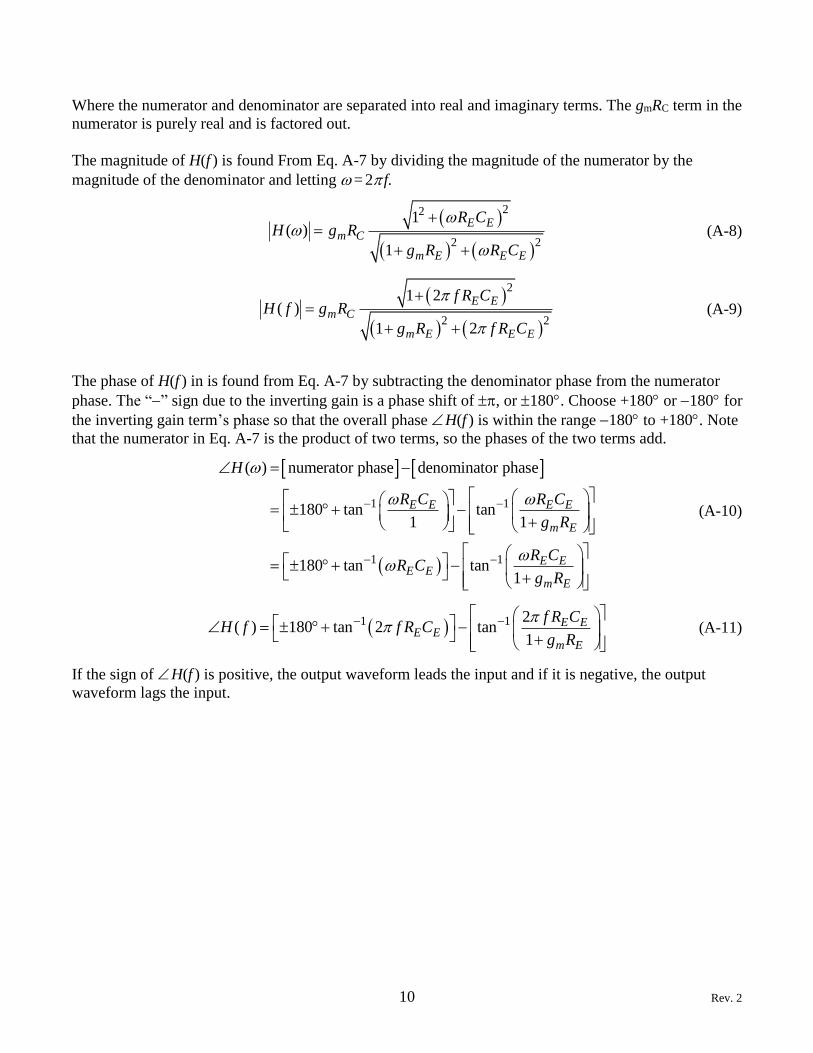
10 Rev. 2
Where the numerator and denominator are separated into real and imaginary terms. The gmRC term in the
numerator is purely real and is factored out.
The magnitude of H(f ) is found From Eq. A-7 by dividing the magnitude of the numerator by the
magnitude of the denominator and letting = 2 f.
( )
( ) ( )
22
2 2
1( )
1
E Em C
m E E E
R CH g R
g R R C
+=
+ +
(A-8)
( )
( ) ( )
2
2 2
1 2( )
1 2
E Em C
m E E E
f R CH f g R
g R f R C
+=
+ +
(A-9)
The phase of H(f ) in is found from Eq. A-7 by subtracting the denominator phase from the numerator
phase. The “−” sign due to the inverting gain is a phase shift of , or 180. Choose +180 or −180 for
the inverting gain term’s phase so that the overall phase H(f ) is within the range −180 to +180. Note
that the numerator in Eq. A-7 is the product of two terms, so the phases of the two terms add.
( )
1 1
1 1
( ) numerator phase denominator phase
180 tan tan1 1
180 tan tan1
E E E E
m E
E EE E
m E
H
R C R C
g R
R CR C
g R
− −
− −
= −
= + −
+
= + − +
(A-10)
( )1 1 2( ) 180 tan 2 tan
1
E EE E
m E
f R CH f f R C
g R
− −
= + − +
(A-11)
If the sign of H(f ) is positive, the output waveform leads the input and if it is negative, the output
waveform lags the input.