Embed Size (px)
Citation preview
Lab on a Chip
CRITICAL REVIEW
Cite this: Lab Chip, 2015, 15, 4256
Received 10th July 2015,Accepted 15th September 2015
DOI: 10.1039/c5lc00809c
www.rsc.org/loc
Materials for microfabricated implantable devices:a review
Kee Scholten and Ellis Meng*
The application of microfabrication to the development of biomedical implants has produced a new
generation of miniaturized technology for assisting treatment and research. Microfabricated implantable
devices (μID) are an increasingly important tool, and the development of new μIDs is a rapidly growing field
that requires new microtechnologies able to safely and accurately function in vivo. Here, we present a
review of μID research that examines the critical role of material choice in design and fabrication. Materials
commonly used for μID production are identified and presented along with their relevant physical
properties and a survey of the state-of-the-art in μID development. The consequence of material choice
as it pertains to microfabrication and biocompatibility is discussed in detail with a particular focus on the
divide between hard, rigid materials and soft, pliable polymers.
1. IntroductionBiomedical devices intended for in vivo implantation,whether diagnostic or therapeutic, face familiar challenges of
4256 | Lab Chip, 2015, 15, 4256–4272 This journal is © The Royal Society of Chemistry 2015
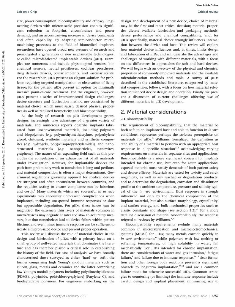
Kee Scholten
Kee Scholten is a postdoctoralscholar in the department of Bio-medical Microsystems Labora-tory at the University of South-ern California. Kee graduatedfrom the California Institute ofTechnology (Caltech) in May2009 with a BS in Applied Phys-ics. He completed his PhD inApplied Physics at the Universityof Michigan under ProfessorEdward Zellers in 2014, with afocus on opto/microfluidic sen-sors for gas-phase micro-devices.
His research interests are in microfluidic sensors, and the synthe-sis of microfabricated devices with nanoscale structures.
Ellis Meng
Ellis Meng is Professor of bio-medical and electrical engineer-ing in the Viterbi School of Engi-neering at the University ofSouthern California. She is alsoDwight C. and Hildagarde E.Baum Chair of the Departmentof Biomedical Engineering. Shereceived the B.S. degree in engi-neering and applied science andthe M.S. and Ph.D. degrees inelectrical engineering from theCalifornia Institute of Technol-ogy (Caltech), Pasadena, in
1997, 1998, and 2003, respectively. She directs the BiomedicalMicrosystems Laboratory founded in 2004 which conductsresearch on biocompatible polymer technology and micro-machining, sensors and actuators, microfluidics, and implantableand biomedical microelectromechanical systems (MEMS). Herhonors include the NSF CAREER award, Wallace H. Coulter Foun-dation Early Career Award, 2009 TR35 Young Innovator Under35, Viterbi Early Career Chair, and ASEE Curtis W. McGrawResearch Award. She is on the editorial board of the Journal ofMicromechanics and Microengineering and is co-chair of the 2017IEEE MEMS conference. She is also an active educator andauthored a textbook on bioMEMS.
Department of Biomedical Engineering, Univ. of Southern California, Los Angeles,CA 90089-1111, USA. E-mail: [email protected]
Publ
ished
on
15 S
epte
mbe
r 201
5. D
ownl
oade
d by
Uni
vers
ity o
f Sou
ther
n Ca
lifor
nia
on 1
8/05
/201
7 20
:09:
49.
View Article OnlineView Journal | View Issue
Lab Chip, 2015, 15, 4256–4272 | 4257This journal is © The Royal Society of Chemistry 2015
size, power consumption, biocompatibility and efficacy. Engi-neering devices with micron-scale precision enables signifi-cant reduction in footprint, encumbrance and powerdemand, and an accompanying increase in device complexityand often capability. By adapting semiconductor micro-machining processes to the field of biomedical implants,researchers have opened broad new avenues of research andpromulgated a generation of new implantable technologies,so-called microfabricated implantable devices (μID). Exam-ples are numerous and include physiological sensors, bio-chemical sensors, neural prostheses, cochlear prostheses,drug delivery devices, ocular implants, and vascular stents.For the researcher, μIDs present an elegant solution for prob-lems requiring targeted manipulation or observation of livingtissue; for the patient, μIDs present an option for minimallyinvasive point-of-care treatment. For the engineer, however,μIDs present a series of interconnected design challenges;device structure and fabrication method are constrained bymaterial choice, which must satisfy desired physical proper-ties as well as required hermeticity and biocompatibility.
As the body of research on μID development grows,designs increasingly take advantage of a greater variety ofmaterials, and numerous reports describe implants fabri-cated from unconventional materials, including polymersand biopolymers (e.g. polymethylmethacrylate, polyethyleneglycol, chitosan), synthetic materials and synthetic compos-ites (e.g. hydrogels, polyIJN-isopropylacrylamide)), and nano-structured materials (e.g. nanoparticles, nanowires,graphene). The nature of an expanding field such as this pre-cludes the compilation of an exhaustive list of all materialsunder investigation. However, for implantable devices thepath from preliminary work to translation is long and perilous,and material composition is often a major determinant. Gov-ernment regulations governing approval for medical devicesare stringent and often inconsistent between countries, andthe requisite testing to ensure compliance can be laboriousand costly.1 Many materials which are successful in in vitroexperiments may encounter unforeseen complications whenimplanted, including unexpected immune responses or slowbut appreciable degradation. For μIDs, these issues can bemagnified; the extremely thin layers of materials common inmicro-devices may degrade at rates too slow to accurately mea-sure, but that nonetheless lead to device failure within patientlifetime, and even minor immune response can be sufficient toisolate a micron-sized device and prevent proper operation.
This review will discuss the role of material choice in thedesign and fabrication of μIDs, with a primary focus on asmall group of well-vetted materials that dominates the litera-ture and has therefore played a critical role in establishingthe history of the field. For ease of analysis, we have broadlycharacterized those surveyed as either ‘hard’ or ‘soft’, theformer comprising high Young's moduli materials such assilicon, glass, metals and ceramics and the latter comprisinglow Young's moduli polymers including polydimethylsiloxane(PDMS), polyimide, polyIJchloro-p-xylylene) (Parylene C), andbiodegradable polymers. For engineers embarking on the
design and development of a new device, choice of materialmay be the first and most critical decision; material proper-ties dictate available fabrication and packaging methods,device performance and chemical compatibility, and, forμIDs specifically, material choice strongly influences interac-tion between the device and host. This review will explorehow material choice influences and, at times, limits designand fabrication of μIDs, and will describe the advantages andchallenges of working with different materials, with a focuson the differences in approaches for soft and hard devices.We will begin with an overview of the physical and chemicalproperties of commonly employed materials and the availablemicrofabrication methods and tools. A survey of μIDsdescribed in the established literature, categorized by mate-rial composition, follows, with a focus on how material selec-tion influenced device design and operation. Finally, we pres-ent a discussion of current challenges affecting use ofdifferent materials in μID development.
2. Material considerations2.1 Biocompatibility
The requirement of biocompatibility, that the material beboth safe to an implanted host and able to function in in vivoconditions, represents perhaps the strictest prerequisite onmaterials for μIDs.2 Williams formalized the definition as“the ability of a material to perform with an appropriate hostresponse in a specific situation”,3 acknowledging varyingrequirements on materials in separate sites and applications.Biocompatibility is a more significant concern for implantsintended for chronic use, but even for acute applications,exposed material must satisfy demands of both patient safetyand device efficacy. Materials are tested for toxicity and carci-nogenicity, as well as any leached or degradation products,and to determine the degradation, corrosion and dissolutionprofile at the ambient temperature, pressure and salinity typi-cal of the in vivo environment. Host response is stronglyinfluenced not only by the chemical composition of theimplant material, but also surface morphology, crystallinity,and surface energy, and bulk mechanical properties such aselastic constants and shape (see section 2.2).4 For a moredetailed discussion of material biocompatibility, the reader isreferred to reviews by Williams.4,5
Biocompatibility requirements exclude many materialscommon in microfabrication and microelectromechanicalsystems (MEMS) for μIDs; many metals corrode quickly inin vivo environments6 while polymers with low melting orsoftening temperatures, or high solubility in water, failmechanically. For μIDs intended for chronic implantation,there are considerations of water and gas intrusion,7 fatiguefailure,8 and failure due to immune response.9–11 Scar forma-tion and other foreign body reactions present a significantobstacle to long-term implantation,9,11 and are a commonfailure mode for otherwise successful μIDs. Common strate-gies to countering (or limiting) the immune response includecareful design and implant placement, minimizing size to
Lab on a Chip Critical review
Publ
ished
on
15 S
epte
mbe
r 201
5. D
ownl
oade
d by
Uni
vers
ity o
f Sou
ther
n Ca
lifor
nia
on 1
8/05
/201
7 20
:09:
49.
View Article Online
4258 | Lab Chip, 2015, 15, 4256–4272 This journal is © The Royal Society of Chemistry 2015
reduce tissue damage, biomolecular coatings,12,13 and phar-maceutical approaches;14–16 however, choice of materialremains critical.17
Common examples of materials considered biocompatibleand used in μIDs include: cobalt-chromium, iridium, tita-nium, platinum, nitinol, certain glasses, PDMS, Parylene C,polymethylmethacrylate (PMMA) and polyimide.1,7,18,19 Sili-con, polysilicon, SU-8 polymer, SiO2, Si3N4, and SiC have beentested by Kotzar et al. under regulatory guidelines (FDA ISO10-993), and minimal biocompatibility issues were reportedfor all but SU-8.20 Subsequent tests of implanted devices like-wise suggest silicon to be a viable material for μIDs,9,21 how-ever such data falls short of what is needed for regulatoryapproval. Extensive data on histopathology for corticalimplants specifically was compiled by Stensaas andStensaas,22 and organizes materials as non-reactive (e.g. alu-minum, ceramic alumina, gold, platinum and certain produc-tions of polyethylene and Teflon), reactive (e.g. SiO2,nichrome, TiO2) and toxic (e.g. Silastic RTV silicone, silver,iron and copper).
Due to concerns of electrochemical corrosion, biofoulingand irritation, micromachined devices are frequently encap-sulated in conformal polymers, bonded to glass, or enclosedin biocompatible metal casings.23 Encapsulation is a com-mon approach even for devices comprising exclusively bio-compatible materials, as an insulating or hermetic seal isoften required to prevent water and soluble ions from damag-ing or shorting electrical connections. Material choice forencapsulants must satisfy not only conditions of biocompati-bility, but also desired low permeability, ease of deposition,and conformality.
2.2 Physical properties
As with any MEMS device, material selection must accountfor any necessary constraints on mechanical, electrical, ther-mal, optical and chemical properties, but there are oftenrequirements of material properties unique to μIDs. For
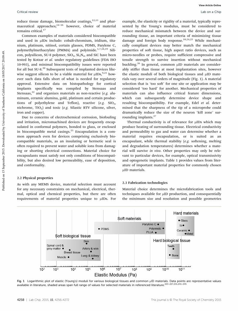
example, the elasticity or rigidity of a material, typically repre-sented by the Young's modulus, must be considered toreduce mechanical mismatch between the device and sur-rounding tissue, an important criteria of minimizing tissuedamage and foreign body response.10,24,25 While mechani-cally compliant devices may better match the mechanicalproperties of soft tissue, high aspect ratio devices, such asmicro-needles or probes, require sufficient compressive andtensile strength to survive insertion without mechanicalbuckling.26 In general, common μID materials are consider-ably stiffer than tissue at most implantation sites, howeverthe elastic moduli of both biological tissues and μID mate-rials vary over several orders of magnitude (Fig. 1). A materialselection that is ‘too soft’ for one site or application may beconsidered ‘too hard’ for another. Mechanical properties ofmaterials can also influence critical feature dimensions,which can subsequently determine device shape andresulting biocompatibility. For example, Edel et al. deter-mined that the sharpness of the tip of a microprobe coulddramatically reduce the size of the neuron ‘kill zone’ sur-rounding implants.27
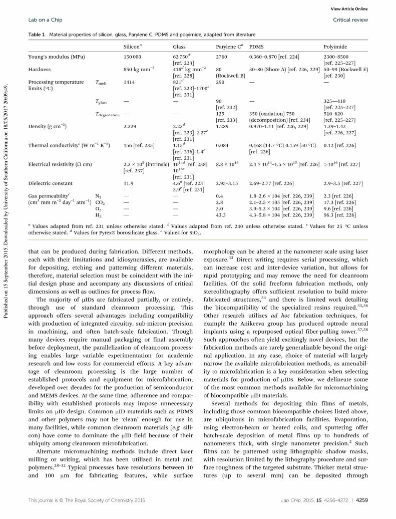
Thermal conductivity is of relevance for μIDs which mayproduce heating of surrounding tissue. Electrical conductivityand permeability to gas and water can determine whether amaterial requires encapsulation, or is suited as anencapsulant, while thermal stability (e.g. softening, meltingand degradation temperatures) determines whether a mate-rial will survive in vivo. Other properties may only be rele-vant to particular devices, for example, optical transmissivityand optogenetic implants. Table 1 provides values from liter-ature of important material properties for commonly chosenμID materials.
2.3 Fabrication technologies
Material choice determines the microfabrication tools andtechniques available for μID production, and consequentiallythe minimum size and resolution and possible geometries
Fig. 1 Logarithmic plot of elastic (Young's) moduli for various biological tissues and common μID materials. Data points are representative valuesavailable in literature, shaded areas span full range of values for selected materials in referenced literature.223–227,231,241–245
Lab on a ChipCritical review
Publ
ished
on
15 S
epte
mbe
r 201
5. D
ownl
oade
d by
Uni
vers
ity o
f Sou
ther
n Ca
lifor
nia
on 1
8/05
/201
7 20
:09:
49.
View Article Online
Lab Chip, 2015, 15, 4256–4272 | 4259This journal is © The Royal Society of Chemistry 2015
that can be produced during fabrication. Different methods,each with their limitations and idiosyncrasies, are availablefor depositing, etching and patterning different materials,therefore, material selection must be coincident with the ini-tial design phase and accompany any discussions of criticaldimensions as well as outlines for process flow.
The majority of μIDs are fabricated partially, or entirely,through use of standard cleanroom processing. Thisapproach offers several advantages including compatibilitywith production of integrated circuitry, sub-micron precisionin machining, and often batch-scale fabrication. Thoughmany devices require manual packaging or final assemblybefore deployment, the parallelization of cleanroom process-ing enables large variable experimentation for academicresearch and low costs for commercial efforts. A key advan-tage of cleanroom processing is the large number ofestablished protocols and equipment for microfabrication,developed over decades for the production of semiconductorand MEMS devices. At the same time, adherence and compat-ibility with established protocols may impose unnecessarylimits on μID design. Common μID materials such as PDMSand other polymers may not be ‘clean’ enough for use inmany facilities, while common cleanroom materials (e.g. sili-con) have come to dominate the μID field because of theirubiquity among cleanroom microfabrication.
Alternate micromachining methods include direct lasermilling or writing, which has been utilized in metal andpolymers.28–32 Typical processes have resolutions between 10and 100 μm for fabricating features, while surface
morphology can be altered at the nanometer scale using laserexposure.33 Direct writing requires serial processing, whichcan increase cost and inter-device variation, but allows forrapid prototyping and may remove the need for cleanroomfacilities. Of the solid freeform fabrication methods, onlystereolithography offers sufficient resolution to build micro-fabricated structures,34 and there is limited work detailingthe biocompatibility of the specialized resins required.35,36
Other research utilizes ad hoc fabrication techniques, forexample the Anikeeva group has produced optrode neuralimplants using a repurposed optical fiber-pulling tower.37,38
Such approaches often yield excitingly novel devices, but thefabrication methods are rarely generalizable beyond the origi-nal application. In any case, choice of material will largelynarrow the available microfabrication methods, as amenabil-ity to microfabrication is a key consideration when selectingmaterials for production of μIDs. Below, we delineate someof the most common methods available for micromachiningof biocompatible μID materials.
Several methods for depositing thin films of metals,including those common biocompatible choices listed above,are ubiquitous in microfabrication facilities. Evaporation,using electron-beam or heated coils, and sputtering offerbatch-scale deposition of metal films up to hundreds ofnanometers thick, with single nanometer precision.2 Suchfilms can be patterned using lithographic shadow masks,with resolution limited by the lithography procedure and sur-face roughness of the targeted substrate. Thicker metal struc-tures (up to several mm) can be deposited through
Table 1 Material properties of silicon, glass, Parylene C, PDMS and polyimide, adapted from literature
Silicona Glass Parylene Cb PDMS Polyimide
Young's modulus (MPa) 150 000 62 750d
[ref. 223]2760 0.360–0.870 [ref. 224] 2300–8500
[ref. 225–227]Hardness 850 kg mm−2 418d kg mm−2
[ref. 228]80(Rockwell B)
30–80 (Shore A) [ref. 226, 229] 50–99 (Rockwell E)[ref. 230]
Processing temperaturelimits (°C)
Tmelt 1414 821d
[ref. 223]–1700e
[ref. 231]
290 — —
Tglass — — 90[ref. 232]
— 325—410[ref. 225–227]
Tdegredation — — 125[ref. 233]
350 (oxidation) 750(decomposition) [ref. 234]
510–620[ref. 225–227]
Density (g cm−3) 2.329 2.23d
[ref. 223]–2.27e
[ref. 231]
1.289 0.970–1.11 [ref. 226, 229] 1.39–1.42[ref. 226, 227]
Thermal conductivityc (W m−1 K−1) 156 [ref. 235] 1.15d
[ref. 236]–1.4e
[ref. 231]
0.084 0.168 (14.7 °C) 0.159 (50 °C)[ref. 226]
0.12 [ref. 226]
Electrical resistivity (Ω cm) 2.3 × 10⁵ (intrinsic)[ref. 237]
1014d [ref. 238]1016e
[ref. 231]
8.8 × 10¹⁶ 2.4 × 10¹⁴–1.5 × 10¹⁵ [ref. 226] >1016 [ref. 227]
Dielectric constant 11.9 4.6d [ref. 223]3.9e [ref. 231]
2.95–3.15 2.69–2.77 [ref. 226] 2.9–3.5 [ref. 227]
Gas permeabilityc
(cm3 mm m−2 day−1 atm−1)N2 — — 0.4 1.8–2.6 × 10⁴ [ref. 226, 239] 2.3 [ref. 226]CO2 — — 2.8 2.1–2.5 × 10⁵ [ref. 226, 239] 17.3 [ref. 226]O2 — — 3.0 3.9–5.3 × 10⁴ [ref. 226, 239] 9.6 [ref. 226]H2 — — 43.3 4.3–5.8 × 10⁴ [ref. 226, 239] 96.3 [ref. 226]
a Values adapted from ref. 231 unless otherwise stated. b Values adapted from ref. 240 unless otherwise stated. c Values for 25 °C unlessotherwise stated. d Values for Pyrex® borosilicate glass. e Values for SiO2.
Lab on a Chip Critical review
Publ
ished
on
15 S
epte
mbe
r 201
5. D
ownl
oade
d by
Uni
vers
ity o
f Sou
ther
n Ca
lifor
nia
on 1
8/05
/201
7 20
:09:
49.
View Article Online
4260 | Lab Chip, 2015, 15, 4256–4272 This journal is © The Royal Society of Chemistry 2015
electroplating, however this requires electrically conductivesubstrates and can result in rough surfaces or other defects.2
Materials such as silicon, silicon nitride, silicon dioxide, andsome polymers (e.g. Parylene), can be deposited conformallyby way of chemical vapor deposition (CVD).2,39 Thoughnumerous different incarnations of the process exist, mostrequire high temperatures and low pressures and all requirean available chemical precursor. CVD processes offer a highdynamic range of thickness, from monolayers to tens ofmicrons, high uniformity and excellent conformality, butmay not be compatible with all substrates or materials, andare not amenable to shadow masking.39 Polymeric materialssuch as PDMS and polyimide can be deposited in wet pro-cesses, or cast from solvents or uncured states.40 Spin-coating offers highly uniform, but non-conformal, coverageof substrates at thicknesses ranging from single to hundredsof microns. Greater conformality can be afforded by castingdirectly from an uncured state, but uniformity is sacrificed.40
For those materials not easily patterned during deposi-tion, the availability of useful etching techniques is critical. Alarge variety of tested techniques exist for silicon etching,including isotropic and anisotropic wet etchants, isotropicgas etchants, isotropic plasma etchants, and deep reactiveion etches (DRIE), many with high selectivity and etch rates,facilitating surface and bulk micromachining for MEMS fab-rication. However, for other materials common in μID devel-opment, options are often limited. Glass can be etched iso-tropically by HF and anisotropically with DRIE processesusing SF6 or C4F8,
41–43 but etch rates for the latter are consid-erably slower than those achievable with silicon. Polyimideand Parylene are typically patterned with reactive ion etches(RIE) and oxygen containing plasmas,44–49 as wet etching, inmost cases, is not feasible.46,50 Typical masking materials(i.e. photoresists) etch at similar rates, unfortunately withselectivity as low as 1 : 1 and thereby limiting etch depth.47
DRIE of Parylene can be achieved with cycles of SF6 and O2
plasma followed by C4F8, but reported aspect ratios are poorcompared to silicon DRIE.51 PDMS is notoriously difficult toetch, due to its high chemical inertness. Dry etching methodsexist that use reactive ion or microwave generated plasmas ofCF4 and O2 mixtures,52,53 however many of these methodssuffer from slow etch rates and poor aspect ratios, and oftenyield rough surfaces.
Few MEMS or μIDs comprise a single homogeneous mate-rial, as such compatibility with other materials and materialprocessing, strength of inter-material adhesion and availabil-ity of bonding methods is a chief concern. For materialsrequiring a biocompatible or hermetic seal for chronicimplantation, but are nonetheless commonly used in μIDs(e.g. silicon), adhesion strength and durability withencapsulants is critical. For silicon μIDs, several reports havedescribed adhesion with conformal coatings of silicone rub-bers,54,55 Parylene,55–59 and polyimide,60 as well as methodsfor creating long-lasting hermetically sealed devices withanodic bonding to glass.59,61,62 An excellent comparative anal-ysis by Treager of encapsulant efficacy against moisture
intrusion highlights the superiority of metals and glassesover organic adhesives and silicones.63 A thorough reviewspecific to silicon μID encapsulation has been compiled byWasikiewicz and Roohpour.55 For polymeric materials adhe-sion strength and surface area has been noted to improvewith plasma exposure or the use of adhesion promotors suchas silane A-174.56 Inter-material bonding and compatibility isalso important for hybrid devices, where multiple materialsserve structural purposes beyond encapsulation; these mate-rial interfaces include glass-silicon,64–67 glass-Parylene,68 sili-con-polyimide,69 and silicon-Parylene.70 Reliability of inter-material bonding is also critical for packaging and assemblyof microfabricated components. For a detailed description ofestablished methods for micropackaging and microassemblyof μIDs the reader is directed to texts by Schuettler and Stieg-litz,71 and Inmann and Hodgins.72
3. ‘Hard’ materials for microfabricatedimplantable devices‘Hard’ materials, representing those non-polymeric materialswith high Young's moduli (>104 MPa), high hardness (>102
kg mm−2), high working temperatures (>500 °C), and effec-tively zero gas or liquid permeability, include silicon, glass,ceramics, and metals, the most common materials used inMEMS production and historically the first materials used forproducing μIDs. As early as 1970, researchers were adaptingsemiconductor manufacturing processes to create simpleimplantable electrodes for recording neural activity.73 Follow-ing the onset of MEMS research and development, siliconmicromachining was used to produce the first μID pressuresensors,74,75 drug delivery devices,76,77 and neural electrodearrays.78,79 Glass and metal structures became commonlyused in conjunction with silicon μIDs, providing biocompati-ble or hermetic encapsulation, or serving as mechanical orelectrical components. More recently microfabricated devicescomprising only glass or metal structures have grown in pop-ularity, owing to new fabrication methods such as glassreflow,80 and laser milling.29 Due to widespread familiaritywith silicon micromachining, and the importance of compati-bility with CMOS processing and integrated circuitry (IC), sili-con remains the most common choice of material for μIDfabrication. Hard materials, in general, are favored for theirmechanical strength, large thermal budget, and impermeabil-ity to liquid intrusion.
Hard μIDs are typically produced by way of bulk and/orsurface micromachining of preformed substrates. Bulk micro-machining typically relies upon chemical etchants or physicalmachining methods to produce mechanically robust, highaspect-ratio three-dimensional structures for implantableMEMS, while surface micromachining methods include UVand electron-beam lithography, thin-film deposition (e.g.CVD, sputtering and evaporation of metals, dielectrics andpolymers), oxide growth, and dopant implantation, withapplications for patterning planar devices such as electrodesor circuit components. Through combinations of these
Lab on a ChipCritical review
Publ
ished
on
15 S
epte
mbe
r 201
5. D
ownl
oade
d by
Uni
vers
ity o
f Sou
ther
n Ca
lifor
nia
on 1
8/05
/201
7 20
:09:
49.
View Article Online
Lab Chip, 2015, 15, 4256–4272 | 4261This journal is © The Royal Society of Chemistry 2015
methods, an impressive number of hard μIDs have beendeveloped and tested: electrochemical and optical probes forstimulating and recording neural activity, drug deliverydevices, physical, chemical and electrical sensors, and pros-theses. This section will review microfabrication approachesfor a popular subset of hard substrates, namely silicon,glasses, ceramics and metals, as they pertain to the develop-ment of μIDs, and examine the challenges of using suchmaterials.
3.1 Silicon
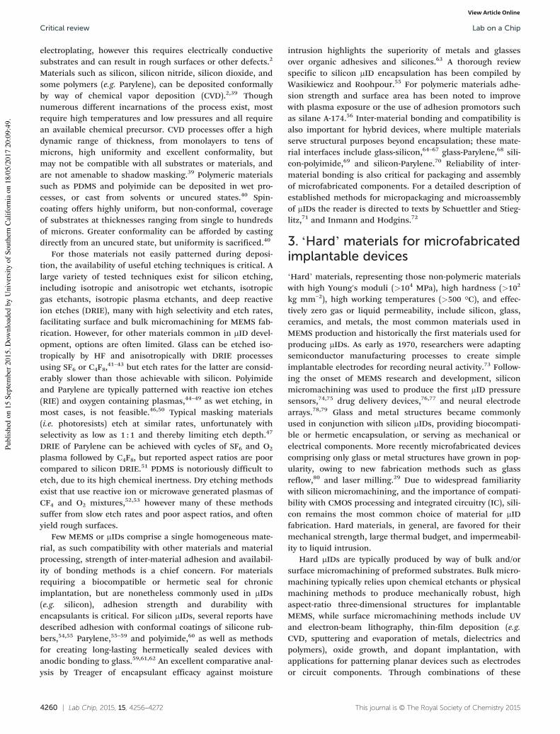
Though best known for its semiconducting properties, siliconis commonly used in μID production as a mechanical mate-rial or bulk substrate due to the ease with which it can bemicromachined with high resolution and repeatability. Sev-eral μIDs produced through silicon micromachining are
presented in Fig. 2. Wet etching of bulk silicon through litho-graphically patterned mask layers provides a low-cost, batchscalable method for fabricating a variety of desired structureson a micrometer size scale. Examples of such structuresinclude simple cavities. Several variations of wireless μIDpressure sensors comprise silicon cavities vacuum sealed bysilicon–silicon fusion bonding or silicon-glass anodicbonding.65,66,75,81–85 The design, adapted for biomedical useby Bäcklund et al. in 1990,75 consists of a vacuum sealed cavityenclosed on at least one side by a thin membrane; deflectionsin the membrane due to changes in physiological pressure aremeasured capacitively65,66,75,81–84 or piezoelectrically.85 Thedesign is robust and versatile, facilitates simple integration ofplanar metal coils for wireless monitoring, and was success-fully employed for monitoring intraocular75,83 and cardiovascu-lar pressures.82,84,85
A similar fabrication approach was used to produce reser-voir cavities for implantable drug delivery/releasedevices.9,77,86–89 Santini et al. used KOH, an anisotropic etch-ant, to create implantable arrays of square pyramidal micro-reservoirs sealed with individually addressed membranes thatcould be electrochemically dissolved for controlled, in vivorelease of therapeutics such as polypetides.77,89 Elman et al.used similar KOH etched reservoirs with release driven byelectro-thermal destruction of the sealing silicon nitridemembrane; the design has shown success in intracranialdelivery of chemotherapeutics in rodent models.86,87 Thesedesigns allow for large numbers of individually addressable,low-volume reservoirs in a solid-state device, though the reli-ance on concentration based diffusion makes controllingdosing rate difficult.
Micromachining of silicon is also used to fabricate high-aspect ratio shanks, as a structure for penetrating neuralprobes. μID neural probes comprise long and thin supportstructures patterned with conductive electrodes for electro-chemical recording and/or stimulation of brain tissue orperipheral nerves. There has been considerable work on sili-con neural probes and neural probe arrays, with the devicesknown as the ‘Utah array’ and ‘Michigan array’ being themost successful. The ‘Utah array’, an intracortical microelec-trode array composed of metal-tipped silicon needles, is fab-ricated by isotropically etching mechanically-cut silicon col-umns in a series of acid baths (5% HF, 95% HNO3).
79,90,91
This process tapers the columns into thin needles with sharptips, enabling penetration into the neural cortex. The ‘Michi-gan array’ consists of electrode coated microprobes fabri-cated from stacked layers of boron doped silicon, SiO2, Si3N4,and patterned metal traces, released from a silicon wafer byetching away the undoped silicon with ethylenediamine-pyro-catechol.78,92 This is a versatile method that enables fabrica-tion of very thin devices; in one report, the approach wasadapted to produce a flexible electrode array for a cochlearprosthesis.93,94 These methods provide for batch-scale, paral-lel fabrication of high-aspect ratio structures, with preciselycontrolled shank dimensions and electrode impedances andplacement. The selection of silicon enables the fabrication of
Fig. 2 Examples of microfabricated implantable devices machinedfrom silicon. (a) Intracortical recording electrode array: reprinted fromref. 91 © Elsevier 1998. (b) KOH etched silicon drug release microchip:reprinted from ref. 9 © Elsevier 2003. (c) Cochlear prosthesisstimulating electrode (inset) connected to application specificintegrated circuit: reprinted from ref. 94 © Elsevier 2008.
Lab on a Chip Critical review
Publ
ished
on
15 S
epte
mbe
r 201
5. D
ownl
oade
d by
Uni
vers
ity o
f Sou
ther
n Ca
lifor
nia
on 1
8/05
/201
7 20
:09:
49.
View Article Online
4262 | Lab Chip, 2015, 15, 4256–4272 This journal is © The Royal Society of Chemistry 2015
sharp probes that easily penetrate brain tissue, and easesconnection to ancillary electronics.
In addition to wet etchants, dry silicon etchants, includingisotropic XeF2 gas, ionized plasma, and highly anisotropicDRIE methods (e.g. Bosch processes), offer controlled micro-machining with high selectivity for many masking mate-rials.95,96 Dry micromachining of silicon avoids issues inher-ent to wet fabrication such as stiction, and DRIE enablesimproved control of etch profile, however these processes fre-quently require serial processing and expensive instruments.These techniques are increasingly used to produce high-aspect ratio silicon structures with sharp features for MEMSdevices, which includes several examples of μIDs such asmicroelectrode shanks for neural recording97,98 and implant-able micromechanical pumps for drug delivery.99
In addition to its role as a support substrate or mechani-cal material in MEMS devices, silicon is the dominant choiceof semiconductor for fabrication of application specific inte-grated circuitry (ASIC) for μID controls. Use of silicon ICs inbiomedical implants predates the development of implant-able MEMS by some years, and examples include convention-ally fabricated devices such as pacemakers, neuro- and mus-cular-stimulators, and middle ear and cochlear auditoryprostheses.100 Inclusion of silicon ASICs in μIDs has becomea critical component of powered devices, particularly thosefor chronic implantation requiring circuitry for wireless com-munication and battery charging, in addition to control anddata logging. A more thorough discussion of IC technology inimplants, and biotelemetry in particular, can be found inreviews by Ko et al.100 and Receveur et al.101 ASICs and trans-ducers are frequently fabricated separately then packagedtogether, and as such choice of other materials for μID fabri-cation does not preclude use of silicon controls. However,direct integration of control circuitry is possible with siliconμIDs, and offers reduced device profiles.102,103
3.2 Glass
Glasses, including borosilicate glasses such as Pyrex, quartz,thermally grown or deposited SiO2, and silicon oxynitride, arefrequently used for sealing or encapsulating silicon μIDs dueto their high impermeability, chemical inertness, and bio-compatibility. In addition, glasses and oxides are excellentelectrical insulators, which is desirable for wirelessly interro-gated μIDs that require electrical insulation of micro-fabricated transmission coils or antennae. Biostability, how-ever, can range greatly depending on specific compositionand even deposition method,104 and several glasses have highdissolution rates in saline. Dissolution rates in vivo have beenmeasured as low as 0.33 nm per day for CVD silicon nitride,and as high as 3.5 nm per day for CVD silicon oxide.105 Intests of subretinal implants, a TEOS oxide (tetra-ethylortho-silicate) layer 0.5 μm thick dissolved entirely, leading to cor-rosion of the underlying silicon device, following one year ofimplantation.106 Evidently the formation of pinhole-free, low-defect layers is necessary for oxide insulated devices intended
for chronic implantation. Alternatively, glass encapsulationmay make use of considerably thicker layers; accelerated agetesting on Pyrex-sealed silicon devices by the Najafi groupextrapolated lifetimes of greater than 100 years.107,108
Though glass is compatible with many lithographic andsurface patterning techniques, bulk micromachining of glassis considerably more arduous compared with silicon. Etchingtechniques for glasses include wet etching, dry etching, andDRIE as well as physical ablation methods such assandblasting, however, in general, these approaches lack therequisite combination of scalability, high resolution, and/orhigh etch rates for ease of fabrication. As such, there are lim-ited though notable examples of glass μIDs. A cooperativeeffort by Allen and CardioMEMS™ produced a passive,implantable pressure sensor for chronic arterial monitoring,fabricated by sealing an LC resonator within a glass etchedcavity.109 The approach was similar to silicon designsdescribed above; HF was used to isotopically etch a recessedcavity in glass. Then after electrodepositing a planar metalinductor coil, the cavity was hermetically sealed by a glassplate supporting a corresponding coil. Haque et al. departedfrom this approach and developed a novel glass reflow pro-cess for fabricating an intraocular pressure sensor.80 The pro-cess involves creating a silicon mold using a DRIE Bosch pro-cess, anodically bonding the etched silicon to a Pyrex wafer,and then heating the Pyrex such that the glass reflows intothe etched features. The silicon is then etched away, leavingbehind a smooth, homogeneous glass structure with highresolution features. Using this method, Haque et al. fabri-cated a glass μID housing an antennae, battery, ASIC, andthe capacitive diaphragm pressure sensor for chronic moni-toring of intraocular pressure.80
A characteristic high optical transparency helped establishglass as the material of choice for commercial fiber opticsand subsequently the material of choice for optical μIDresearch. The use of fiber optics in endoscopic surgery hasincreased familiarity with the technology among medical pro-fessionals, motivating the development of all-glass pressureand temperature sensors fabricated on fiber tips. Suchdevices rely on micromachined Fabry–Perot cavities or Bragggratings to create sensitive transducers for in vivo conditions.Increasingly, the field of optogenetics utilizes μIDs compris-ing glass fibers or waveguides for exciting light-sensitive pro-teins or detecting fluorescence in neural research. Followinginitial efforts relying on unmodified commercial fibers,110–112
the development of micromachined glass optical probesoffered spatially focused stimulation easily paired with sili-con electrode probes. Zhang et al. used HF to taper an opticalfiber to a sharp point, and gold deposition to create an opti-cal aperture of approximately 1 μm.113 The ‘optrode’ (Fig. 3a)was manually integrated with a commercial silicon neuralprobe array to create a combined optical and electrical probefor simultaneous excitation and monitoring of the light sensi-tive channelrhodopsin protein.113 Subsequent efforts adaptedthis approach for other optogenetic circuits and animalmodels, as well as devices with multiple optrodes.114–116
Lab on a ChipCritical review
Publ
ished
on
15 S
epte
mbe
r 201
5. D
ownl
oade
d by
Uni
vers
ity o
f Sou
ther
n Ca
lifor
nia
on 1
8/05
/201
7 20
:09:
49.
View Article Online

Lab Chip, 2015, 15, 4256–4272 | 4263This journal is © The Royal Society of Chemistry 2015
Abaya et al. recently presented an alternative fabricationmethod that used a combination of wet etching and mechan-ical dicing to create an optrode array from a single quartzsubstrate.117 Other glass μIDs for optogenetic research uselithographic patterning to create embedded microfabricatedwaveguides; Wu et al. presented a method for creating opticalwaveguides comprising an oxynitride core clad in SiO2.
118
Such designs offer greater integration with lithographicallypatterned electrodes, but require more complex fabrication.
3.3 Ceramic
Owing to a lack of suitable etching and micro-patterningmethods, there are few examples of ceramic μIDs despite thesuccessful use of the material in medical implants such aship prostheses.119 Ceramic packaging of microfabricateddevices has been adopted for implants, as new techniquesallow for a high density of electrical feed-throughs whilemaintaining impressively low permeability to water.120–122
Similarly, low-temperature co-fired ceramics (LTCC) havefound applications as the support substrate for multilayerimplantable ASICs and antennae, particularly for devicesrequiring wireless telemetry.123–125 The high dielectric con-stant of ceramic, and the ease with which low-profile, multi-layer devices can be fabricated, have helped transitionceramic devices to in vivo applications.
Work from the Gerhardt group has demonstrated the suit-ability of ceramics as a μID substrate for more varied devices.Examples include electrochemical sensors for glutamatedetection126–128 and single neuron recording.129 Typicaldevices consist of ceramic shanks, terminating in tips <5 μmwide, with micro-patterned platinum electrodes on one orboth128 sides (Fig. 3b). Advantages include high mechanicaldurability and biocompatibility, and a decrease in shuntcapacitance compared to silicon electrodes as a result of the
superior electrical insulation. Devices are fabricated by litho-graphically patterning metal electrodes and then individuallycarving each probe using a diamond blade.130 Devices arefinally released individually by mechanically dicing the sub-strate, underscoring the lack of methods for etching throughthick ceramic substrates. This approach requires serial pro-cessing and may not be amenable to the production of manytypes of geometries; as such, there are still limited applica-tions for ceramic μIDs.
3.4 Metal
Several metals have well established biocompatibility and a his-tory of successful use in implanted medical devices, notablytitanium and platinum, but also iridium, nitinol, some stain-less steel variants, and other alloys. These metals exhibitexcellent stability in vivo as well as excellent impermeability,and have long been the material of choice of hermetic sealsaround ‘large’ implants such as pacemakers. However, theneed for wirelessly powered or wirelessly charged μIDs oftenprecludes metal packaging, as opaqueness to electromagneticradiation renders it unsuitable. Metals offer high mechanicalstrength and, unlike silicon, glass, or ceramics, low risk ofbrittle fracture, and therefore a lower risk of catastrophicmechanical failure. These features make metals an enticingchoice of material for μIDs, though the characteristic highconductivity of most metals complicates the design of anydevice requiring surface patterned electronics. As such, useof metals for μID fabrication is typically reserved for applica-tions requiring simple devices and robust structures, such ascoronary stents. Laser milling of stainless steel is a commonapproach, but requires serial processing and provides limitedresolution.28,131 Electrical discharge machining (EDM) is analternative method that offers improved resolution and thepossibility of batch processing.132 The technique involvesgenerating electric spark discharge from microelectrodes tomill away material from a conductive substrates.132 EDM hasbeen successfully used to fabricate several stainless steel μIDsincluding novel variations on coronary stents82,132,133
(Fig. 3c) and also blood vessel cuffs for in vivo flow measure-ments.134,135 Fofonoff et al. demonstrated the use of EDM toproduce a high density array of titanium microprobes forneural recording.136 EDM fabricated titanium columns wereetched with HCl to create a tapered tip only a few micronsacross, and then electroplated with platinum to provide aconductive surface. The probes were insulated with a confor-mal layer of Parylene and the insulation at the tips removedby laser ablation to create the recording electrode site. Arrayswere mechanically robust with precise spacing, but the singleelectrode-site design limited applications.
Subsequent work has led to multi-site metal neural probesby utilizing fabrication methods compatible with lithographicpatterning. Motta et al. used electroplating to create nickelshanks with platinum recording electrodes insulated by sili-con nitride.137 However, devices required an additional goldencapsulation layer to prevent potentially dangerous leaching
Fig. 3 Examples of microfabricated implantable devices machinedfrom glass, ceramic, and metal. (a) Glass fiber ‘optrode’ for opticalneural stimulation: reprinted from ref. 113 © IOP Publishing 2009. (b)Ceramic shank electrode for electrochemical sensing of L-glutamate:reprinted from ref. 126 © Elsevier 2002. (c) Arterial stent fabricatedfrom stainless steel with electro-discharge machining: reprinted fromref. 133 © Springer 2011.
Lab on a Chip Critical review
Publ
ished
on
15 S
epte
mbe
r 201
5. D
ownl
oade
d by
Uni
vers
ity o
f Sou
ther
n Ca
lifor
nia
on 1
8/05
/201
7 20
:09:
49.
View Article Online
4264 | Lab Chip, 2015, 15, 4256–4272 This journal is © The Royal Society of Chemistry 2015
of nickel ions into the brain. An alternative approach byMcCarthy et al. takes advantage of recent advances in reactiveion etching of titanium138 to bulk micromachine probes fromlithographically patterned titanium substrates.139,140
3.5 Challenges of hard materials
The selection of hard materials incurs certain challenges,specific to μID applications, which must be taken intoaccount during the design phase. Several such challengesrelate to issues of biocompatibility. For example, the majorityof the devices surveyed in this section require the addition ofan encapsulating barrier material to provide electrical insula-tion, to shield the body from potentially harmful materials orto reduce protein adhesion and biofouling. Considerablework and literature has been dedicated to ameliorating thisrequirement, and numerous encapsulating methods andmaterials are available, including oxides, polyurethane,PDMS, Parylene and polyimide. Still, it remains a necessaryadditional step, and researchers must be cognizant of con-cerns including adhesion and conformality of the barrierlayer, unwanted changes to electrical or electromagneticproperties, and additional processing steps needed touncover critical features. Sharp edges or corners and hardsurfaces intrinsic to hard materials are also of concern, asthey can tear tissue during surgical placement or whileimplanted. Additionally, severe mismatch between themechanical properties of such materials and the tissue at thetargeted site is believed to induce trauma, resulting frommicro-motion of the hard implant damaging surrounding tis-sue, and exacerbating the immune system's foreign-bodyresponse. Numerous reports, compiled in reviews by Polikovand Navarro,10,141 describe efforts to reduce such damagethrough changes in design or electrode coating, but fre-quently, the stiff material composing the device is identifiedas the problem.24,25,142 The high rigidity and stiffness of hardmaterials can also impede fabrication of devices requiringflexible or deformable components. For μIDs such as nerve‘cuffs’, which require membranes with high mechanical com-pliance, hard materials are ill-suited.
4. ‘Soft’ materials for microfabricatedimplantable devicesHere we define ‘soft’ materials as those with low Young'smoduli (<104 MPa) and low hardness (<102 kg mm−2). Com-pared to silicon and glass these materials have lower thermalconductivity, lower density, and much greater mechanicalcompliance. Soft materials commonly used in biomedicalimplants include many plastics and rubbers, however thissection will focus on those materials with a demonstratedamenability to microfabrication techniques and history ofuse in μID research, namely Parylene C, PDMS, and poly-imide. Additional characteristics of such soft materialsinclude constrained working temperatures (<350 °C), highchemical inertness, and susceptibility to gas and vapor
intrusion. Notably, these materials have well-documentedbiocompatibility (many polymers are used in FDA approvedmedical implants), with negligible issues of cytotoxicity, cor-rosion or instability, and as such have been used for decadesin conventional medical implants. Synthetic polymers and sili-cone rubbers, such as PDMS in particular, have long been afamiliar choice for construction or coating of implantablecatheters, shunts, fluidic valves, bladders, and cosmeticimplants among others, due to ease of fabrication, low cost,and minimal foreign body response incurred by implanta-tion.143,144 Parylene and polyimide found early applicationsas insulating coatings for implantable electrodes,145–148 andbecame increasingly common choices as biomedical encapsu-lation following studies confirming chronic biocompatibil-ity.149,150 μIDs utilizing soft materials became a topic ofincreasing focus in the 1990s, following the proliferation ofpolymer MEMS and spurred in part by the development ofreplica molding and soft lithographic techniques. “Free-film”devices, comprising soft material substrates, offer a combina-tion of high biocompatibility, high flexibility, optical trans-parency, and electrical insulation that motivated continuedresearch. Following improvements in deposition and pattern-ing methods, numerous soft μIDs were developed, which to-date include flexible neural implants, retinal prosthetics,pressure sensors, and drug pumps. More recent efforts havefocused on use of soft biodegradable materials, such as silkfibroin, and the first examples of fully biodegradable and bio-resorbable μIDs have been demonstrated.151
4.1 Surface micromachining of polymers: Parylene,polyimide & PDMS
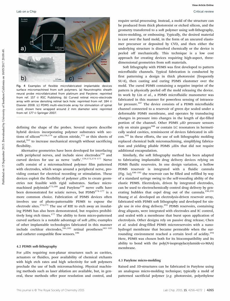
Fabrication of soft μIDs may entail surface micromachiningof planar films or soft-lithographic molding to create three-dimensional or raised structures. The former entails deposit-ing planar layers of polymers onto hard substrates (typicallysilicon wafers) using spin coating or CVD, and then usingphotolithography to pattern additional layers of metal, insu-lation and other materials. Several examples of devices fabri-cated in this manner are displayed in Fig. 4. This approachallows for production of very thin, flexible devices, frequentlyhousing planar electrodes for electrochemical sensing orstimulation. The technique is well suited for the developmentof flexible neural interfaces; the combination of thin profile,robust electrical insulation, and greater mechanical compli-ance addresses several problems facing hard μID neuralinterfaces and conventional microwire probes. Numerousreports have described a range of devices fabricated usingParylene152–159 or polyimide69,160–172 films, and in someinstances PDMS173–177 and liquid crystal polymer.178 Themost common design archetype is a thin penetrating shankcomposed of a polymer-metal-polymer sandwich intended forimplantation in the brain.69,153–158,161–164,166–168,171,179 Typicalfabrication relies on photolithography to pattern metal (fre-quently platinum) for electrodes and connective traces, andO2 RIE for exposing the electrodes from insulation and
Lab on a ChipCritical review
Publ
ished
on
15 S
epte
mbe
r 201
5. D
ownl
oade
d by
Uni
vers
ity o
f Sou
ther
n Ca
lifor
nia
on 1
8/05
/201
7 20
:09:
49.
View Article Online
Lab Chip, 2015, 15, 4256–4272 | 4265This journal is © The Royal Society of Chemistry 2015
defining the shape of the probes. Several reports describehybrid devices incorporating polymer substrates with sec-tions of silicon69,156,179 or silicon nitride,171 or thin sheets ofmetal,163 to increase mechanical strength without sacrificingflexibility.
Alternative geometries have been developed for interfacingwith peripheral nerves, and include sieve electrodes170 andcurved devices for use as nerve ‘cuffs’.159,172,174–177 Nervecuffs consist of a micromachined polymer film patternedwith electrodes, which wraps around a peripheral nerve, pro-viding contact for electrical recording or stimulation. Thesedevices exploit the flexibility of polymer μIDs to create geom-etries not feasible with rigid substrates. Surface micro-machined polyimide172,180 and Parylene159 nerve cuffs havebeen demonstrated for sciatic nerves, but PDMS174–177 is amore common choice. Fabrication of PDMS devices ofteninvolves use of photo-patternable PDMS to expose theelectrode sites.174,175 The use of RIE to etch away an insulat-ing PDMS has also been demonstrated, but requires prohibi-tively long etch times.177 The ability to form micro-patternedcurved surfaces is a notable advantage of soft μIDs; examplesof other implantable technologies fabricated in this mannerinclude cochlear electrodes,181,182 retinal prostheses183–185
and catheter compatible flow sensors.186
4.2 PDMS soft-lithography
For μIDs requiring non-planar structures such as cavities,actuators or fluidics, poor availability of chemical etchantswith high etch rates and high selectivity for soft polymerspreclude the use of bulk micromachining. Physical machin-ing methods such as laser ablation are available, but, in gen-eral, these methods offer poor resolution and control, and
require serial processing. Instead, a mold of the structure canbe produced from thick photoresist or etched silicon, and thegeometry transferred to a soft polymer using soft-lithography,micro-molding, or embossing. Typically, the desired materialis cast over the hard mold, in the form of an uncured elasto-mer precursor or deposited by CVD, and then either theunderlying structure is dissolved chemically or the device ispeeled off mechanically. This technique is a low costapproach for creating devices requiring high-aspect, three-dimensional geometries from soft materials.
Soft lithography with PDMS was first developed to patternmicrofluidic channels. Typical fabrication is conducted byfirst patterning a design in thick photoresist (frequentlySU-8), then casting and curing PDMS elastomer over themold. The cured PDMS containing a negative imprint of thepattern is physically peeled off the mold releasing the device.In work by Lin et al., a PDMS microfluidic manometer wasfabricated in this manner for powerless sensing of intraocu-lar pressure.187 The device consists of a PDMS microfluidicchannel connected to a reservoir of green dye sealed under adeformable PDMS membrane, and operates by transducingchanges in pressure into changes in the length of dye-filledportion of the channel. Other PDMS μID pressure sensorsrely on strain gauges188 or contain LC resonators in hermeti-cally sealed cavities, reminiscent of devices fabricated in sili-con.189 In these efforts, the use of soft lithographic moldingreplaced chemical bulk micromachining, simplifying fabrica-tion and yielding pliable PDMS μIDs that did not requireadditional encapsulation.
Similarly, the soft lithography method has been adaptedto fabricating implantable drug delivery devices relying onPDMS fluidic reservoirs. In one design variation, a hollowPDMS reservoir is integrated with a fluidic cannula(Fig. 5a);190–192 the reservoir can be filled and refilled by wayof a standard syringe owing to the self-resealing ability of theelastic PDMS. Electrolysis, driven by integrated electrodes,can be used to electrochemically control drug delivery by gen-erating bubbles that expel drug out of the cannula.190,191
Huang et al. developed an electrolysis-driven reservoir array,fabricated with PDMS soft lithography and developed for sin-gle use in vivo drug delivery.193 PDMS reservoirs, containingdrug aliquots, were integrated with electrodes and IC control,and sealed with a membrane that burst upon application ofelectrolysis. Other designs rely on passive drug release; Chenet al. sealed drug-filled PDMS microreservoirs with a nano-hydrogel membrane that became permeable when the sur-rounding environment reached a certain level of acidity.194
Here, PDMS was chosen both for its biocompatibility and itsability to bond with the polyIJN-isopropylacrylamide-co-MAA)membrane.
4.3 Parylene micro-molding
Raised and 3D-structures can be fabricated in Parylene usingan analogous micro-molding technique; typically a mold ofpatterned sacrificial polymer (e.g. photoresist, polyethylene
Fig. 4 Examples of flexible microfabricated implantable devicessurface micromachined from soft polymers. (a) Neurotrophic sheathneural probe microfabricated from platinum and Parylene: reprintedfrom ref. 157 © RSC Publishing. (b) Curved retinal micro-electrodearray with arrow denoting retinal tack hole: reprinted from ref. 184 ©Elsevier 2008. (c) PDMS multi-electrode array for stimulation of spinalcord, shown here wrapped around 2 mm diameter wire: reprintedfrom ref. 177 © Springer 2007.
Lab on a Chip Critical review
Publ
ished
on
15 S
epte
mbe
r 201
5. D
ownl
oade
d by
Uni
vers
ity o
f Sou
ther
n Ca
lifor
nia
on 1
8/05
/201
7 20
:09:
49.
View Article Online

4266 | Lab Chip, 2015, 15, 4256–4272 This journal is © The Royal Society of Chemistry 2015
glycol) or etched silicon is prepared, and then coatedconformally with Parylene by way of CVD. Following dissolu-tion of the mold or removal of the Parylene by peeling, thegeometry is retained in the Parylene substrate. This tech-nique allows for the fabrication of Parylene cavities, chan-nels, reservoirs as well as more complex shapes with high-aspect ratios, without relying on deep chemical or plasmaetching. Examples of μIDs fabricated in this approach includeseveral variations of intraocular pressure sensors,195–197 includ-ing a micro-molded Bourbon tube design197 and Parylene vari-ants on LC resonator cavities,195,196 and electrochemical pres-sure sensors designed for monitoring hydrocephalus shuntperformance.198,199 A Parylene actuator for an implantable,micro-scale drug pump using a combination of soft lithogra-phy and Parylene micro-molding was developed.68,200,201
The fabrication approach for the bellows requires a PDMSmold that is used to cast stacked disks of polyethylene gly-col (PEG), which are subsequently coated in a thin film ofParylene (Fig. 5b). Dissolving the PEG in water leavesmicrofabricated Parylene bellows, which are installed in afluidic reservoir on-top of electrolysis electrodes. Genera-tion of bubbles actuates the bellows, which displaces theliquid in the reservoir, allowing for precise, targeted deliv-ery in vivo.
Several instances of Parylene based implantable electrodescombine micro-molding with surface micromachining, to cre-ate implantable electrochemical probes with non-planar fea-tures. Examples include flexible electrode probes with micro-fluidic channels,158 ‘sheath’ electrodes153 and hemispherical
electrodes202 that incorporate raised structures to deliveryneurotrophic agents and improve recording impedances.Wang et al. developed Parylene based electrode arrays for ret-inal prosthesis, using micro-molding onto etched siliconstructures to create impressively sharp but flexible probes.203,204
The technique has also been used to create ancillary struc-tures for silicon neural probes, such as an IC ‘pocket’ inte-grated onto a silicon probe array.205
4.4 Biodegradable materials
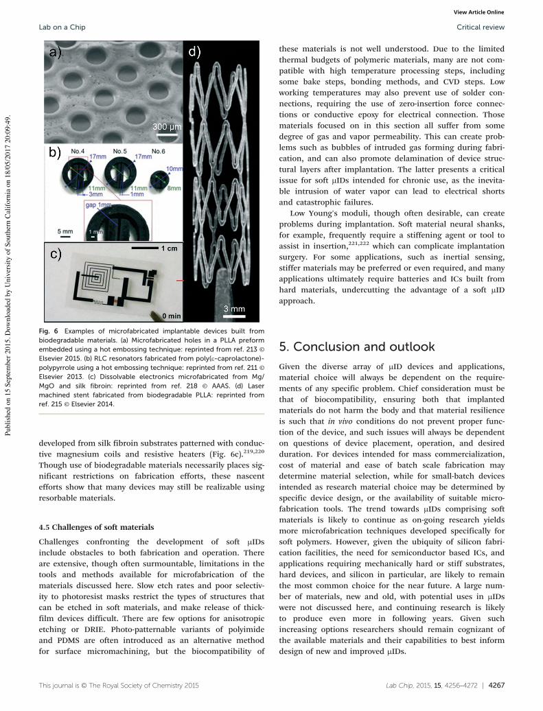
Biomedical implants composed in part or entirely ofbiodegradable materials confer several advantages, includ-ing mitigation of the host's foreign-body response, reductionin size of implant following implantation, dissolution of tem-porary structures needed only during insertion, and oftenobviation of need for explant surgery. The success of biode-gradable polymers in time-release drug delivery capsules anddissolvable sutures has motivated recent work exploring bio-degradable materials for μID fabrication. Several reports onμID neural probes have described the use of biodegradablepolymers such as PEG,157,206 chitosan,207 and silk208,209 astemporary stiffening agents to assist in implantation, how-ever, there have been only a few reports describing the use ofbiodegradable materials as the primary substrate in micro-fabricated implants (Fig. 6). Notable exceptions include workby Grayson et al. on the development of a biodegradabledrug-delivery array;210 the device consists of micro-reservoirsembedded in comparatively slow degrading poly(L-lactic acid)(PLLA), preloaded with different compounds and sealed withthe fast degrading poly(lactic-co-glycolic acid) (PLGA). Fabri-cation entailed compression molding of a PLLA preform witha machined aluminum die. Fig. 6a shows an example of aPLLA preform after the hot embossing process, showing theregularity, but limited resolution, of such fabrication. A simi-lar fabrication method has been used to produce implantableRLC resonators from biodegradable polymers (Fig. 6b),embedded with conductive polypyrrole nanoparticles, for pro-ducing powered, biodegradable μIDs.211,212 Recently, Petersenet al. demonstrated a hot embossing method using an etchedsilicon stamp to produce PLLA drug release devices with sig-nificantly improved resolution over traditional compressionmolding techniques.213 Similar examples of biodegradabledevices include bio-resorbable coronary stents, fabricatedfrom preforms of PLLA and other polymers using direct lasermilling (Fig. 6d).214,215 However, as with compression mold-ing, this approach is compatible with a limited subset of μIDdesigns.
Biodegradable silk membranes offer an enticing alterna-tive. Recent efforts have developed a host of tools for micro-fabrication on biodegradable silk including methods for con-tact printing, soft-lithographic patterning and metaldeposition.216 Several reports outline adapting these methodsto produce biodegradable silk MEMS as optical217 andelectronic218 implantable devices. Fully functional, wirelesslypowered and successfully implanted devices have been
Fig. 5 Examples of microfabricated implantable devices fabricatedwith micro-molded polymers. (a) Refillable drug delivery device forchronic implantation, fabricated through PDMS soft-lithography:reprinted from ref. 192 © RSC Publishing 2008. (b) Microfabricated bel-lows cast from Parylene C onto a polyethylene glycol mold: reprintedfrom ref. 201 © Springer 2012.
Lab on a ChipCritical review
Publ
ished
on
15 S
epte
mbe
r 201
5. D
ownl
oade
d by
Uni
vers
ity o
f Sou
ther
n Ca
lifor
nia
on 1
8/05
/201
7 20
:09:
49.
View Article Online
Lab Chip, 2015, 15, 4256–4272 | 4267This journal is © The Royal Society of Chemistry 2015
developed from silk fibroin substrates patterned with conduc-tive magnesium coils and resistive heaters (Fig. 6c).219,220
Though use of biodegradable materials necessarily places sig-nificant restrictions on fabrication efforts, these nascentefforts show that many devices may still be realizable usingresorbable materials.
4.5 Challenges of soft materials
Challenges confronting the development of soft μIDsinclude obstacles to both fabrication and operation. Thereare extensive, though often surmountable, limitations in thetools and methods available for microfabrication of thematerials discussed here. Slow etch rates and poor selectiv-ity to photoresist masks restrict the types of structures thatcan be etched in soft materials, and make release of thick-film devices difficult. There are few options for anisotropicetching or DRIE. Photo-patternable variants of polyimideand PDMS are often introduced as an alternative methodfor surface micromachining, but the biocompatibility of
these materials is not well understood. Due to the limitedthermal budgets of polymeric materials, many are not com-patible with high temperature processing steps, includingsome bake steps, bonding methods, and CVD steps. Lowworking temperatures may also prevent use of solder con-nections, requiring the use of zero-insertion force connec-tions or conductive epoxy for electrical connection. Thosematerials focused on in this section all suffer from somedegree of gas and vapor permeability. This can create prob-lems such as bubbles of intruded gas forming during fabri-cation, and can also promote delamination of device struc-tural layers after implantation. The latter presents a criticalissue for soft μIDs intended for chronic use, as the inevita-ble intrusion of water vapor can lead to electrical shortsand catastrophic failures.
Low Young's moduli, though often desirable, can createproblems during implantation. Soft material neural shanks,for example, frequently require a stiffening agent or tool toassist in insertion,221,222 which can complicate implantationsurgery. For some applications, such as inertial sensing,stiffer materials may be preferred or even required, and manyapplications ultimately require batteries and ICs built fromhard materials, undercutting the advantage of a soft μIDapproach.
5. Conclusion and outlookGiven the diverse array of μID devices and applications,material choice will always be dependent on the require-ments of any specific problem. Chief consideration must bethat of biocompatibility, ensuring both that implantedmaterials do not harm the body and that material resilienceis such that in vivo conditions do not prevent proper func-tion of the device, and such issues will always be dependenton questions of device placement, operation, and desiredduration. For devices intended for mass commercialization,cost of material and ease of batch scale fabrication maydetermine material selection, while for small-batch devicesintended as research material choice may be determined byspecific device design, or the availability of suitable micro-fabrication tools. The trend towards μIDs comprising softmaterials is likely to continue as on-going research yieldsmore microfabrication techniques developed specifically forsoft polymers. However, given the ubiquity of silicon fabri-cation facilities, the need for semiconductor based ICs, andapplications requiring mechanically hard or stiff substrates,hard devices, and silicon in particular, are likely to remainthe most common choice for the near future. A large num-ber of materials, new and old, with potential uses in μIDswere not discussed here, and continuing research is likelyto produce even more in following years. Given suchincreasing options researchers should remain cognizant ofthe available materials and their capabilities to best informdesign of new and improved μIDs.
Fig. 6 Examples of microfabricated implantable devices built frombiodegradable materials. (a) Microfabricated holes in a PLLA preformembedded using a hot embossing technique: reprinted from ref. 213 ©Elsevier 2015. (b) RLC resonators fabricated from polyIJε-caprolactone)-polypyrrole using a hot embossing technique: reprinted from ref. 211 ©Elsevier 2013. (c) Dissolvable electronics microfabricated from Mg/MgO and silk fibroin: reprinted from ref. 218 © AAAS. (d) Lasermachined stent fabricated from biodegradable PLLA: reprinted fromref. 215 © Elsevier 2014.
Lab on a Chip Critical review
Publ
ished
on
15 S
epte
mbe
r 201
5. D
ownl
oade
d by
Uni
vers
ity o
f Sou
ther
n Ca
lifor
nia
on 1
8/05
/201
7 20
:09:
49.
View Article Online
4268 | Lab Chip, 2015, 15, 4256–4272 This journal is © The Royal Society of Chemistry 2015
Conflict of interest disclosureE. Meng has a significant financial interest in Fluid Syn-chrony LLC.
AcknowledgementsThe authors would like to acknowledge the Viterbi School ofEngineering for support of Dr. Kee Scholten, and the assis-tance of Hsiu (Mike) Yang in preparing the manuscript. Thiswork was partially funded by the NSF under award numberEFRI-1332394.
References1 E. Meng and R. Sheybani, Lab Chip, 2014, 14, 3233–3240.2 M. J. Madou, Fundamentals of microfabrication: the science
of miniaturization, CRC press, 2002.3 D. F. Williams, Definitions in biomaterials: proceedings of a
consensus conference of the European Society forBiomaterials, March 3–5, 1986, Elsevier Science Limited,Chester, England, 1987.
4 D. F. Williams, Biomaterials, 2008, 29, 2941–2953.5 D. F. Williams, Biomaterials, 2009, 30, 5897–5909.6 D. F. Williams, Annu. Rev. Mater. Sci., 1976, 6, 237–266.7 G. Jiang, Front. Neurosci., 2010, 4, 2.8 S. Kisban, D. Moser, B. Rubehn, T. Stieglitz, O. Paul and P.
Ruther, 4th European Conference of the InternationalFederation for Medical and Biological Engineering, 2009.
9 G. Voskerician, M. S. Shive, R. S. Shawgo, H. Von Recum,J. M. Anderson, M. J. Cima and R. Langer, Biomaterials,2003, 24, 1959–1967.
10 V. S. Polikov, P. A. Tresco and W. M. Reichert, J. Neurosci.Methods, 2005, 148, 1–18.
11 J. Turner, W. Shain, D. Szarowski, M. Andersen, S. Martins,M. Isaacson and H. Craighead, Exp. Neurol., 1999, 156, 33–49.
12 L. Norton, H. Koschwanez, N. Wisniewski, B. Klitzman andW. Reichert, J. Biomed. Mater. Res., Part A, 2007, 81, 858–869.
13 L. Norton, E. Tegnell, S. Toporek and W. Reichert,Biomaterials, 2005, 26, 3285–3297.
14 T. Hickey, D. Kreutzer, D. Burgess and F. Moussy,Biomaterials, 2002, 23, 1649–1656.
15 S. D. Patil, F. Papadmitrakopoulos and D. J. Burgess,J. Controlled Release, 2007, 117, 68–79.
16 U. Bhardwaj, R. Sura, F. Papadimitrakopoulos and D. J.Burgess, J. Diabetes Sci. Technol., 2007, 1, 8–17.
17 J. M. Morais, F. Papadimitrakopoulos and D. J. Burgess,AAPS J., 2010, 12, 188–196.
18 V. J. Ablaza and A. S. Breirbart, in Grabb and Smith's PlasticSurgery, ed. C. H. Thome, 2007, ch. 7, pp. 58–65.
19 G. Jiang and D. D. Zhou, in Implantable Neural Prostheses 2,Springer, 2010, pp. 27–61.
20 G. Kotzar, M. Freas, P. Abel, A. Fleischman, S. Roy, C.Zorman, J. M. Moran and J. Melzak, Biomaterials, 2002, 23,2737–2750.
21 A. R. Grayson, R. S. Shawgo, A. M. Johnson, N. T. Flynn, Y.Li, M. J. Cima and R. Langer, Proc. IEEE, 2004, 92, 6–21.
22 S. S. Stensaas and L. Stensaas, Acta Neuropathol., 1978, 41,145–155.
23 L. Yu, B. J. Kim and E. Meng, Sensors, 2014, 14,20620–20644.
24 A. Gilletti and J. Muthuswamy, J. Neural Eng., 2006, 3, 189.25 D. Szarowski, M. Andersen, S. Retterer, A. Spence, M.
Isaacson, H. Craighead, J. Turner and W. Shain, Brain Res.,2003, 983, 23–35.
26 W. Jensen, K. Yoshida and U. G. Hofmann, IEEE Trans.Biomed. Eng., 2006, 53, 934–940.
27 D. J. Edel, V. Toi, V. M. McNeil and L. D. Clark, IEEE Trans.Biomed. Eng., 1992, 39, 635–643.
28 Y. Kathuria, J. Mater. Eng. Perform., 2005, 170, 545–550.29 Y. P. Kathuria, Laser-Assisted Micro-and Nanotechnologies, 2004.30 M. Schuettler, S. Stiess, B. King and G. Suaning, J. Neural
Eng., 2005, 2, S121.31 C. G. K. Malek, Anal. Bioanal. Chem., 2006, 385, 1351–1361.32 C. G. K. Malek, Anal. Bioanal. Chem., 2006, 385, 1362–1369.33 A. Vorobyev and C. Guo, Appl. Surf. Sci., 2007, 253, 7272–7280.34 F. P. Melchels, J. Feijen and D. W. Grijpma, Biomaterials,
2010, 31, 6121–6130.35 T. Matsuda and M. Mizutani, J. Biomed. Mater. Res.,
2002, 62, 395–403.36 V. Popov, A. Evseev, A. Ivanov, V. Roginski, A. Volozhin and
S. Howdle, J. Mater. Sci.: Mater. Med., 2004, 15, 123–128.37 C. Lu, U. P. Froriep, R. A. Koppes, A. Canales, V. Caggiano,
J. Selvidge, E. Bizzi and P. Anikeeva, Adv. Funct. Mater.,2014, 24, 6594–6600.
38 P. Anikeeva, A. S. Andalman, I. Witten, M. Warden, I.Goshen, L. Grosenick, L. A. Gunaydin, L. M. Frank and K.Deisseroth, Nat. Neurosci., 2012, 15, 163–170.
39 R. Ghodssi and P. Lin, MEMS Materials and ProcessesHandbook, Springer Science & Business Media, 2011.
40 C. Liu, Adv. Mater., 2007, 19, 3783–3790.41 X. Li, T. Abe and M. Esashi, Sens. Actuators, A, 2001, 87,
139–145.42 J. Park, N.-E. Lee, J. Lee, J. Park and H. Park, Microelectron.
Eng., 2005, 82, 119–128.43 K. Kolari, V. Saarela and S. Franssila, J. Micromech.
Microeng., 2008, 18, 064010.44 U. Buder, J.-P. von Klitzing and E. Obermeier, Sens.
Actuators, A, 2006, 132, 393–399.45 B. Mimoun, H. T. Pham, V. Henneken and R. Dekker,
J. Vac. Sci. Technol., B, 2013, 31, 021201.46 K. R. Williams, K. Gupta and M. Wasilik,
J. Microelectromech. Syst., 2003, 12, 761–778.47 E. Meng, P.-Y. Li and Y.-C. Tai, J. Micromech. Microeng.,
2008, 18, 045004.48 J. Yeh and K. Grebe, J. Vac. Sci. Technol., A, 1983, 1, 604–608.49 B. P. Levy, S. L. Campbell and T. L. Rose, IEEE Trans.
Biomed. Eng., 1986, 1046–1049.50 Technical Paper published by Specialty Coating Systems,
Solvent Resistance of Parylenes, published 2001, accessedMarch 3rd 2015, (http://scscoatings.com/corporate/library.aspx).
51 E. Meng, S. Aoyagi and Y.-C. Tai, Spec. Publ. - R. Soc. Chem.,2004, 297, 401–403.
Lab on a ChipCritical review
Publ
ished
on
15 S
epte
mbe
r 201
5. D
ownl
oade
d by
Uni
vers
ity o
f Sou
ther
n Ca
lifor
nia
on 1
8/05
/201
7 20
:09:
49.
View Article Online

Lab Chip, 2015, 15, 4256–4272 | 4269This journal is © The Royal Society of Chemistry 2015
52 S. J. Hwang, D. J. Oh, P. G. Jung, S. M. Lee, J. S. Go, J.-H.Kim, K.-Y. Hwang and J. S. Ko, J. Micromech. Microeng.,2009, 19, 095010.
53 J. Garra, T. Long, J. Currie, T. Schneider, R. White and M.Paranjape, J. Vac. Sci. Technol., A, 2002, 20, 975–982.
54 P. E. Donaldson, Med. Biol. Eng. Comput., 1989, 27, 93–94.55 J. Wasikiewicz and N. Roohpour, Implantable Sensor
Systems for Medical Applications, 2013, 68.56 C. Hassler, R. P. von Metzen, P. Ruther and T. Stieglitz,
J. Biomed. Mater. Res., Part B, 2010, 93, 266–274.57 J.-M. Hsu, L. Rieth, R. A. Normann, P. Tathireddy and F.
Solzbacher, IEEE Trans. Biomed. Eng., 2009, 56, 23–29.58 D. Feili, M. Schuettler, T. Doerge, S. Kammer and T.
Stieglitz, Sens. Actuators, A, 2005, 120, 101–109.59 K. Najafi, Proceedings of the IEEE Sensors Conference, 2007,
pp. 58–63.60 S. Schmidt, K. Horch and R. Normann, J. Biomed. Mater.
Res., 1993, 27, 1393–1399.61 B. Ziaie, J. A. Von Arx, M. R. Dokmeci and K. Najafi,
J. Microelectromech. Syst., 1996, 5, 166–179.62 T. J. Harpster and K. Najafi, Micro Electro Mechanical
Systems, The Fifteenth IEEE International Conference on, 2002.63 R. K. Traeger, IEEE Trans. Parts, Hybrids, Packag., 1977, 13,
147–152.64 A. D. DeHennis and K. D. Wise, J. Microelectromech. Syst.,
2006, 15, 678–685.65 E.-C. Park, J.-B. Yoon and E. Yoon, Jpn. J. Appl. Phys.,
1998, 37, 7124–7128.66 O. Akar, T. Akin and K. Najafi, Sens. Actuators, A, 2001, 95,
29–38.67 K. Takahata, A. DeHennis, K. D. Wise and Y. B.
Gianchandani, Micro Electro Mechanical Systems, 17th IEEEInternational Conference on (MEMS), 2004.
68 H. Gensler, R. Sheybani, P.-Y. Li, R. L. Mann and E. Meng,Biomed. Microdevices, 2012, 14, 483–496.
69 K.-K. Lee, J. He, A. Singh, S. Massia, G. Ehteshami, B. Kimand G. Raupp, J. Micromech. Microeng., 2004, 14, 32.
70 P.-J. Chen, D. C. Rodger, S. Saati, M. S. Humayun and Y.-C.Tai, J. Microelectromech. Syst., 2008, 17, 1342–1351.
71 M. Schuettler and T. Stieglitz, Implantable Sensor Systemsfor Medical Applications, 2013, 108.
72 A. Inmann and D. Hodgins, Implantable Sensor Systems forMedical Applications, Elsevier, 2013.
73 K. D. Wise, J. B. Angell and A. Starr, IEEE Trans. Biomed.Eng., 1970, 238–247.
74 K. Van Schuylenbergh, E. Peeters, B. Puers, W. Sansen and A.Neetens, 1st European Conference on Biomedical Engineering, 1991.
75 Y. Bäcklund, L. Rosengren, B. Hök and B. Svedbergh, Sens.Actuators, A, 1990, 21, 58–61.
76 D. Maillefer, H. van Lintel, G. Rey-Mermet and R. Hirschi,Micro Electro Mechanical Systems, Twelfth IEEEInternational Conference on, 1999.
77 J. T. Santini, M. J. Cima and R. Langer, Nature, 1999, 397,335–338.
78 K. L. Drake, K. Wise, J. Farraye, D. Anderson and S.BeMent, IEEE Trans. Biomed. Eng., 1988, 35, 719–732.
79 P. K. Campbell, K. E. Jones, R. J. Huber, K. W. Horch andR. A. Normann, IEEE Trans. Biomed. Eng., 1991, 38, 758–768.
80 R.-U. Haque and K. D. Wise, J. Microelectromech. Syst.,2013, 22, 1470–1477.
81 T. Eggers, C. Marschner, U. Marschner, B. Clasbrummel, R.Laur and J. Binder, Micro Electro Mechanical Systems, TheThirteenth Annual International Conference on, 2000.
82 K. Takahata, A. DeHennis, K. D. Wise and Y. B.Gianchandani, Proceedings of IEEE MEMS Conference, 2004,pp. 216–219.
83 L. Rosengren, P. Rangsten, Y. Bäcklund, B. Hök, B.Svedbergh and G. Selén, Sens. Actuators, A, 1994, 43, 55–58.
84 A. DeHennis and K. D. Wise, Micro Electro MechanicalSystems, The Fifteenth IEEE International Conference on,2002.
85 E. Kalvesten, L. Smith, L. Tenerz and G. Stemme, MicroElectro Mechanical Systems, The Eleventh AnnualInternational Workshop on, 1998.
86 N. Elman, B. Masi, M. Cima and R. Langer, Lab Chip,2010, 10, 2796–2804.
87 B. C. Masi, B. M. Tyler, H. Bow, R. T. Wicks, Y. Xue, H.Brem, R. Langer and M. J. Cima, Biomaterials, 2012, 33,5768–5775.
88 J. M. Maloney, S. A. Uhland, B. F. Polito, N. F. Sheppard,C. M. Pelta and J. T. Santini, J. Controlled Release,2005, 109, 244–255.
89 J. H. Prescott, S. Lipka, S. Baldwin, N. F. Sheppard, J. M.Maloney, J. Coppeta, B. Yomtov, M. A. Staples and J. T.Santini, Nat. Biotechnol., 2006, 24, 437–438.
90 K. E. Jones, P. K. Campbell and R. A. Normann, Ann.Biomed. Eng., 1992, 20, 423–437.
91 P. J. Rousche and R. A. Normann, J. Neurosci. Methods,1998, 82, 1–15.
92 R. J. Vetter, J. C. Williams, J. F. Hetke, E. A. Nunamakerand D. R. Kipke, IEEE Trans. Biomed. Eng., 2004, 51,896–904.
93 P. T. Bhatti and K. D. Wise, IEEE J. Solid-State Circuits,2006, 41, 2965–2973.
94 K. D. Wise, P. T. Bhatti, J. Wang and C. R. Friedrich, Hear.Res., 2008, 242, 22–30.
95 G. T. Kovacs, N. I. Maluf and K. E. Petersen, Proc. IEEE,1998, 86, 1536–1551.
96 J. Miao, in Encyclopedia of Microfluidics and Nanofluidics,ed. D. Li, Springer, US, 2008, ch. 1412, pp. 1840–1846, DOI:10.1007/978-0-387-48998-8_1412.
97 P. Norlin, M. Kindlundh, A. Mouroux, K. Yoshida and U. G.Hofmann, J. Micromech. Microeng., 2002, 12, 414.
98 W. Pei, L. Zhu, S. Wang, K. Guo, J. Tang, X. Zhang, L. Lu, S.Gao and H. Chen, Sci. China, Ser. E: Technol. Sci., 2009, 52,1187–1190.
99 L. Cao, S. Mantell and D. Polla, Sens. Actuators, A, 2001, 94,117–125.
100 W. Ko and P. Feng, Handbook of Mems for Wireless andMobile Applications, 2013, p. 401.
101 R. A. Receveur, F. W. Lindemans and N. F. de Rooij,J. Micromech. Microeng., 2007, 17, R50.
Lab on a Chip Critical review
Publ
ished
on
15 S
epte
mbe
r 201
5. D
ownl
oade
d by
Uni
vers
ity o
f Sou
ther
n Ca
lifor
nia
on 1
8/05
/201
7 20
:09:
49.
View Article Online
4270 | Lab Chip, 2015, 15, 4256–4272 This journal is © The Royal Society of Chemistry 2015
102 O. Brand, Proc. IEEE, 2006, 94, 1160–1176.103 G. K. Fedder, R. T. Howe, T.-J. K. Liu and E. P. Quevy, Proc.
IEEE, 2008, 96, 306–322.104 M. Vogt and R. Hauptmann, Surf. Coat. Technol., 1995, 74,
676–681.105 J. M. Maloney, S. A. Lipka and S. P. Baldwin, Proceedings of the
Material Research Society Symposium, 2005, pp. J14.3.1–14.3.6.106 H. Hämmerle, K. Kobuch, K. Kohler, W. Nisch, H. Sachs
and M. Stelzle, Biomaterials, 2002, 23, 797–804.107 M. Dokmeci, J. Von Arx and K. Najafi, Proceedings of
International Conference on Solid-State Sensors andActuators, 1997, pp. 283–286.
108 T. J. Harpster and K. Najafi, Proceedings of the IEEE MEMSConference, 2002, pp. 100–107.
109 M. G. Allen, Solid-State Sensors, Actuators and Microsystems,The 13th International Conference on, 2005.
110 R. Pashaie and R. Falk, IEEE Trans. Biomed. Eng., 2013, 60,268–280.
111 F. Zhang, V. Gradinaru, A. R. Adamantidis, R. Durand,R. D. Airan, L. de Lecea and K. Deisseroth, Nat. Protoc.,2010, 5, 439–456.
112 A. M. Aravanis, L.-P. Wang, F. Zhang, L. A. Meltzer, M. Z.Mogri, M. B. Schneider and K. Deisseroth, J. Neural Eng.,2007, 4, S143.
113 J. Zhang, F. Laiwalla, J. A. Kim, H. Urabe, R. Van Wagenen,Y.-K. Song, B. W. Connors, F. Zhang, K. Deisseroth andA. V. Nurmikko, J. Neural Eng., 2009, 6, 055007.
114 S. Royer, B. V. Zemelman, M. Barbic, A. Losonczy, G.Buzsáki and J. C. Magee, Eur. J. Neurosci., 2010, 31,2279–2291.
115 J. Wang, F. Wagner, D. A. Borton, J. Zhang, I. Ozden, R. D.Burwell, A. V. Nurmikko, R. Van Wagenen, I. Diester and K.Deisseroth, J. Neural Eng., 2012, 9, 016001.
116 I. Ozden, J. Wang, Y. Lu, T. May, J. Lee, W. Goo, D. J.O'Shea, P. Kalanithi, I. Diester and M. Diagne, J. Neurosci.Methods, 2013, 219, 142–154.
117 T. Abaya, M. Diwekar, S. Blair, P. Tathireddy, L. Rieth, G.Clark and F. Solzbacher, SPIE BiOS, 2013, p. 85860V-5.
118 F. Wu, E. Stark, M. Im, I.-J. Cho, E.-S. Yoon, G. Buzsáki,K. D. Wise and E. Yoon, J. Neural Eng., 2013, 10, 056012.
119 I. C. Clarke, Clin. Orthop. Relat. Res., 1992, 282, 19–30.120 T. Guenther, C. Kong, H. Lu, M. J. Svehla, N. H. Lovell, A.
Ruys and G. J. Suaning, J. Biomed. Mater. Res., Part B,2014, 102, 500–507.
121 T. Guenther, C. W. Dodds, N. H. Lovell and G. J. Suaning,Proceedings of the IEEE Engineering in Medicine and BiologyConference, 2011, pp. 6717–6720.
122 M. Schuettler, J. S. Ordonez, T. S. Santisteban, A. Schatz, J.Wilde and T. Stieglitz, Proceedings of the IEEE Engineering inMedicine and Biology Conference, 2010, pp. 1585–1588.
123 E. Y. Chow, C.-L. Yang, A. Chlebowski, W. J. Chappell andP. P. Irazoqui, Microwave Symposium Digest, IEEE MTT-SInternational, 2008, pp. 1309–1312.
124 E. Y. Chow, C.-L. Yang, A. Chlebowski, S. Moon, W. J.Chappell and P. P. Irazoqui, IEEE Trans. Microwave TheoryTech., 2008, 56, 3200–3208.
125 N. Vidal, J. L. Villegas, S. Curto, J. Sieiro and F. Ramos,Antennas and Propagation Society International Symposium(APSURSI), 2012.
126 J. J. Burmeister, F. Pomerleau, M. Palmer, B. K. Day, P. Huettland G. A. Gerhardt, J. Neurosci. Methods, 2002, 119, 163–171.
127 J. J. Burmeister and G. A. Gerhardt, Anal. Chem., 2001, 73,1037–1042.
128 E. M. Miller, J. E. Quintero, F. Pomerleau, P. Huettl, G. A.Gerhardt and P. E. Glaser, J. Neurosci. Methods, 2015, in press.
129 K. A. Moxon, S. C. Leiser, G. A. Gerhardt, K. A. Barbee andJ. K. Chapin, IEEE Trans. Biomed. Eng., 2004, 51, 647–656.
130 J. J. Burmeister, K. Moxon and G. A. Gerhardt, Anal. Chem.,2000, 72, 187–192.
131 C. Momma, U. Knop and S. Nolte, Biomedical Research,1999, 4, 39–44.
132 K. Takahata and Y. B. Gianchandani, J. Microelectromech.Syst., 2002, 11, 102–110.
133 D. Lappin, A. R. Mohammadi and K. Takahata, J. Mater.Sci.: Mater. Med., 2012, 23, 349–356.
134 K. Takahata and Y. B. Gianchandani, Electrical and ComputerEngineering, CCECE Canadian Conference on, 2007.
135 K. Takahata and Y. B. Gianchandani, Proc. Solid-State Sen-sor and Actuator Workshop, 2004.
136 T. A. Fofonoff, S. M. Martel, N. G. Hatsopoulos, J. P.Donoghue and I. W. Hunter, IEEE Trans. Biomed. Eng.,2004, 51, 890–895.
137 P. S. Motta and J. W. Judy, IEEE Trans. Biomed. Eng.,2005, 52, 923–933.
138 M. F. Aimi, M. P. Rao, N. C. MacDonald, A. S. Zuruzi andD. P. Bothman, Nat. Mater., 2004, 3, 103–105.
139 P. T. McCarthy, K. J. Otto and M. P. Rao, Biomed.Microdevices, 2011, 13, 503–515.
140 P. McCarthy, M. Rao and K. Otto, J. Neural Eng., 2011, 8, 046007.141 X. Navarro, T. B. Krueger, N. Lago, S. Micera, T. Stieglitz
and P. Dario, J. Peripher. Nerv. Syst., 2005, 10, 229–258.142 H. Lee, R. V. Bellamkonda, W. Sun and M. E. Levenston,
J. Neural Eng., 2005, 2, 81.143 J. Curtis and A. Colas, Biomater. Sci., 2004, 697–707.144 R. Yoda, J. Biomater. Sci., Polym. Ed., 1998, 9, 561–626.145 G. E. Loeb, M. Bak, M. Salcman and E. Schmidt, IEEE
Trans. Biomed. Eng., 1977, 121–128.146 E. Schmidt, J. McIntosh and M. Bak, Med. Biol. Eng.
Comput., 1988, 26, 96–101.147 S. A. Shamma-Donoghue, G. A. May, N. E. Cotter, R. L. White and
F. B. Simmons, IEEE Trans. Electron Devices, 1982, 29, 136–144.148 R. Pickard, P. Joseph, A. Collins and R. Hicks, Med. Biol.
Eng. Comput., 1979, 17, 261–267.149 N. Stark, Medical Plastic and Biomaterials, 1996, 3, 30–35.150 R. Richardson, J. Miller and W. Reichert, Biomaterials,
1993, 14, 627–635.151 J. Bai, T. Ma, W. Chu, R. Wang, L. Silva, C. Michal, J. C.
Chiao and M. Chiao, Biomed. Microdevices, 2006, 8, 317–323.152 S. Takeuchi, D. Ziegler, Y. Yoshida, K. Mabuchi and T.
Suzuki, Lab Chip, 2005, 5, 519–523.153 B. Kim, J. Kuo, S. Hara, C. Lee, L. Yu, C. Gutierrez, T. Hoang,
V. Pikov and E. Meng, J. Neural Eng., 2013, 10, 045002.
Lab on a ChipCritical review
Publ
ished
on
15 S
epte
mbe
r 201
5. D
ownl
oade
d by
Uni
vers
ity o
f Sou
ther
n Ca
lifor
nia
on 1
8/05
/201
7 20
:09:
49.
View Article Online
Lab Chip, 2015, 15, 4256–4272 | 4271This journal is © The Royal Society of Chemistry 2015
154 I. R. Minev, P. Musienko, A. Hirsch, Q. Barraud, N. Wenger,E. M. Moraud, J. Gandar, M. Capogrosso, T. Milekovic andL. Asboth, Science, 2015, 347, 159–163.
155 T. Suzuki, K. Mabuchi and S. Takeuchi, Neural Engineering,First International IEEE EMBS Conference on, 2003.
156 C. Pang, J. G. Cham, Z. Nenadic, S. Musallam, Y.-C. Tai,J. W. Burdick and R. Andersen, Engineering in Medicine andBiology Society, 27th Annual International Conference of the,2005.
157 J. T. Kuo, B. J. Kim, S. A. Hara, C. D. Lee, C. A. Gutierrez,T. Q. Hoang and E. Meng, Lab Chip, 2013, 13, 554–561.
158 D. Ziegler, T. Suzuki and S. Takeuchi, J. Microelectromech.Syst., 2006, 15, 1477–1482.
159 H. Yu, W. Xiong, H. Zhang, W. Wang and Z. Li, MicroElectro Mechanical Systems, IEEE 27th InternationalConference on, 2014.
160 T. Stieglitz, M. Schuettler and J.-U. Meyer, Biomed.Microdevices, 2000, 2, 283–294.
161 M. Im, I.-J. Cho, K.-S. Yun and E. Yoon, Appl. Phys. Lett.,2007, 91, 124101.
162 P. J. Rousche, D. S. Pellinen, D. P. Pivin Jr, J. C. Williams,R. J. Vetter and D. R. Kipke, IEEE Trans. Biomed. Eng.,2001, 48, 361–371.
163 A. A. Fomani and R. R. Mansour, Sens. Actuators, A,2011, 168, 233–241.
164 A. L. Owens, T. J. Denison, H. Versnel, M. Rebbert, M.Peckerar and S. A. Shamma, J. Neurosci. Methods, 1995, 58,209–220.
165 S. Shamma-donoghue, G. May, N. E. Cotter, R. L. Whiteand F. B. Simmons, IEEE Trans. Electron Devices, 1982, 29,136–144.
166 S. Boppart, B. C. Wheeler and C. S. Wallace, IEEE Trans.Biomed. Eng., 1992, 39, 37–42.
167 M. Peckerar, S. A. Shamma, M. Rebbert, J. Kosakowski andP. Isaacson, Rev. Sci. Instrum., 1991, 62, 2276–2280.
168 S. Takeuchi, T. Suzuki, K. Mabuchi and H. Fujita,J. Micromech. Microeng., 2004, 14, 104.
169 T. Stieglitz and J. Meyer, Med. Device Technol., 1998, 10,28–30.
170 T. Stieglitz, H. Beutel and J.-U. Meyer, Sens. Actuators, A,1997, 60, 240–243.
171 C. González and M. Rodríguez, J. Neurosci. Methods,1997, 72, 189–195.
172 J. Zariffa, M. K. Nagai, M. Schuettler, T. Stieglitz, Z. J.Daskalakis and M. R. Popovic, IEEE Trans. Neural Syst.Rehabil. Eng., 2011, 19, 147–156.
173 O. Graudejus, Z. Yu, J. Jones, B. Morrison and S. Wagner,J. Electrochem. Soc., 2009, 156, P85–P94.
174 E. Delivopoulos, D. J. Chew, I. R. Minev, J. W. Fawcett andS. P. Lacour, Lab Chip, 2012, 12, 2540–2551.
175 S. P. Lacour, S. Benmerah, E. Tarte, J. FitzGerald, J. Serra, S.McMahon, J. Fawcett, O. Graudejus, Z. Yu and B. MorrisonIII, Med. Biol. Eng. Comput., 2010, 48, 945–954.
176 J. J. FitzGerald, N. Lago, S. Benmerah, J. Serra, C. P.Watling, R. E. Cameron, E. Tarte, S. B. McMahon and J. W.Fawcett, J. Neural Eng., 2012, 9, 016010.
177 K. W. Meacham, R. J. Giuly, L. Guo, S. Hochman and S. P.DeWeerth, Biomed. Microdevices, 2008, 10, 259–269.
178 S. E. Lee, S. B. Jun, H. J. Lee, J. Kim, S. W. Lee, C. Im, H.-C.Shin, J. W. Chang and S. J. Kim, IEEE Trans. Biomed. Eng.,2012, 59, 2085–2094.
179 E. G. Kim, J. K. John, H. Tu, Q. Zheng, J. Loeb, J. Zhangand Y. Xu, Sens. Actuators, B, 2014, 195, 416–422.
180 M. Schuettler, I. Triantis, B. Rubehn and T. Stieglitz, Proc.12th Ann. Conf. IFESS, 2007.
181 A. C. Johnson and K. D. Wise, Micro Electro MechanicalSystems, IEEE 23rd International Conference on, 2010.
182 P. Deman, T. Kaiser, J. Dirckx, F. Offeciers and S. Peeters,J. Neurosci. Methods, 2003, 128, 143–150.
183 M. Maghribi, J. Hamilton, D. Polla, K. Rose, T. Wilson and P.Krulevitch, Microtechnologies in Medicine; Biology 2nd AnnualInternational IEEE-EMB Special Topic Conference on, 2002.
184 D. C. Rodger, A. J. Fong, W. Li, H. Ameri, A. K. Ahuja, C.Gutierrez, I. Lavrov, H. Zhong, P. R. Menon and E. Meng,Sens. Actuators, B, 2008, 132, 449–460.
185 W. Li, D. C. Rodger, A. Pinto, E. Meng, J. D. Weiland, M. S.Humayun and Y.-C. Tai, Sens. Actuators, A, 2011, 166,193–200.
186 L. Yu, B. J. Kim and E. Meng, Micro Electro MechanicalSystems, 28th IEEE International Conference on, 2015.
187 K.-M. Lin, H. J. Sant, B. K. Ambati and B. K. Gale,Proceedings of the 16th International Conference onMiniaturized Systems for Chemistry and Life Sciences,MicroTAS, Okinawa, Japan, 2012.
188 M. Leonardi, P. Leuenberger, D. Bertrand, A. Bertsch and P.Renaud, Invest. Ophthalmol. Vis., 2004, 45, 3113–3117.
189 A. Sepúlveda, F. Fachin, R. G. de Villoria, B. Wardle, J.Viana, A. Pontes and L. A. Rocha, Procedia Eng., 2011, 25,140–143.
190 Y. Liu, P. Song, J. Liu, D. J. H. Tng, R. Hu, H. Chen, Y. Hu,C. H. Tan, J. Wang and J. Liu, Biomed. Microdevices,2015, 17, 1–12.
191 S. Saati, R. Lo, P.-Y. Li, E. Meng, R. Varma and M. S.Humayun, Trans. Am. Ophthalmol. Soc., 2009, 107, 60.
192 R. Lo, P.-Y. Li, S. Saati, R. Agrawal, M. S. Humayun and E.Meng, Lab Chip, 2008, 8, 1027–1030.
193 P.-L. Huang, P.-H. Kuo, Y.-J. Huang, H.-H. Liao, Y.-J. Yang,T. Wang, Y.-H. Wang and S.-S. Lu, IEEE Trans. Ind.Electron., 2012, 59, 1578–1587.
194 J. Chen, M. Chu, K. Koulajian, X. Y. Wu, A. Giacca and Y.Sun, Biomed. Microdevices, 2009, 11, 1251–1257.
195 J.-H. Lin, Y. Zhao, P.-J. Chen, M. Humayun and Y.-C. Tai,IEEE Nanotechnol Mag., 2012, 6, 8–16.
196 P.-J. Chen, S. Saati, R. Varma, M. S. Humayun and Y.-C.Tai, J. Microelectromech. Syst., 2010, 19, 721–734.
197 P.-J. Chen, D. C. Rodger, R. Agrawal, S. Saati, E. Meng, R.Varma, M. S. Humayun and Y.-C. Tai, J. Micromech.Microeng., 2007, 17, 1931.
198 C. A. Gutierrez and E. Meng, Micro Electro MechanicalSystems, IEEE 24th International Conference on, 2011.
199 L. Yu and E. Meng, Micro Electro Mechanical Systems, IEEE27th International Conference on, 2014.
Lab on a Chip Critical review
Publ
ished
on
15 S
epte
mbe
r 201
5. D
ownl
oade
d by
Uni
vers
ity o
f Sou
ther
n Ca
lifor
nia
on 1
8/05
/201
7 20
:09:
49.
View Article Online
4272 | Lab Chip, 2015, 15, 4256–4272 This journal is © The Royal Society of Chemistry 2015
200 P.-Y. Li, R. Sheybani, C. A. Gutierrez, J. T. Kuo and E. Meng,J. Microelectromech. Syst., 2010, 19, 215–228.
201 R. Sheybani, H. Gensler and E. Meng, Biomed. Microdevices,2013, 15, 37–48.
202 Y. Rui, J. Liu, Y. Wang and C. Yang, Microsyst. Technol.,2011, 17, 437–442.
203 R. Wang, W. Zhao, W. Wang and Z. Li, Micro ElectroMechanical Systems, IEEE 24th International Conference on, 2011.
204 R. Wang, X. Huang, G. Liu, W. Wang, F. Dong and Z. Li,J. Microelectromech. Syst., 2010, 19, 367–374.
205 R. Huang and Y. Tai, IEEE 22nd International Conference onMicro Electro Mechanical Systems, 2009.
206 M. Y. Cheng, K. L. Tan, T. B. Yee and M. Y. Je, Adv. Mater.Res., 2013, 517–522.
207 F. Ceyssens, K. van Kuyck, B. Nuttin and R. Puers, ProcediaEng., 2012, 47, 688–689.
208 F. Wu, L. Tien, F. Chen, D. Kaplan, J. Berke and E. Yoon,Transducers & Eurosensors XXVII: The 17th InternationalConference on Solid-State Sensors, Actuators and Micro-systems, 2013.
209 F. Wu, M. Im and E. Yoon, Solid-State Sensors, Actuatorsand Microsystems Conference, 16th International, 2011.
210 A. C. R. Grayson, I. S. Choi, B. M. Tyler, P. P. Wang, H. Brem,M. J. Cima and R. Langer, Nat. Mater., 2003, 2, 767–772.
211 C. Boutry, H. Chandrahalim, P. Streit, M. Schinhammer, A.Hänzi and C. Hierold, Sens. Actuators, A, 2013, 189, 344–355.
212 C. M. Boutry, W. Sun, T. Strunz, H. Chandrahalim and C.Hierold, Frequency Control Symposium (FCS), IEEEInternational, 2010.
213 R. S. Petersen, R. Mahshid, N. K. Andersen, S. S. Keller,H. N. Hansen and A. Boisen, Microelectron. Eng., 2015, 133,104–109.
214 A. Abizaid and J. R. Costa, Circ.: Cardiovasc. Interventions,2010, 3, 384–393.
215 B. Stępak, A. Antończak, M. Bartkowiak-Jowsa, J. Filipiak, C.Pezowicz and K. Abramski, Archives of Civil and MechanicalEngineering, 2014, 14, 317–326.
216 H. Tao, D. L. Kaplan and F. G. Omenetto, Adv. Mater.,2012, 24, 2824–2837.
217 H. Tao, J. M. Kainerstorfer, S. M. Siebert, E. M. Pritchard,A. Sassaroli, B. J. Panilaitis, M. A. Brenckle, J. J. Amsden, J.Levitt and S. Fantini, Proc. Natl. Acad. Sci. U. S. A.,2012, 109, 19584–19589.
218 S.-W. Hwang, H. Tao, D.-H. Kim, H. Cheng, J.-K. Song, E.Rill, M. A. Brenckle, B. Panilaitis, S. M. Won and Y.-S. Kim,Science, 2012, 337, 1640–1644.
219 H. Tao, S. Hwang, B. Marelli, B. An, J. Moreau, M. Yang, M.Brenckle, S. Kim, D. Kaplan and J. Rogers, Micro ElectroMechanical Systems, 28th IEEE International Conference on, 2015.
220 H. Tao, S.-W. Hwang, B. Marelli, B. An, J. E. Moreau, M.Yang, M. A. Brenckle, S. Kim, D. L. Kaplan and J. A. Rogers,Proc. Natl. Acad. Sci. U. S. A., 2014, 111, 17385–17389.
221 S. Felix, K. Shah, D. George, V. Tolosa, A. Tooker, H. Sheth,T. Delima and S. Pannu, Engineering in Medicine andBiology Society (EMBC), Annual International Conference ofthe IEEE, 2012.
222 S. H. Felix, K. G. Shah, V. M. Tolosa, H. J. Sheth, A. C.Tooker, T. L. Delima, S. P. Jadhav, L. M. Frank and S. S.Pannu, J. Visualized Exp., 2013, e50609.
223 Corning, Glass Silicon Constraint Substrates, http://www.corning.com/lightingmaterials/images/wafersheet.pdf, (accessedMarch 3rd, 2015).
224 D. Armani, C. Liu and N. Aluru, Micro Electro MechanicalSystems, Twelfth IEEE International Conference on, 1999.
225 FujiFilm, Durimide 7000 Technical Product Information,http://www.fujifilmusa.com/shared/bin/Durimide%207000_US12.pdf, (accessed March 3rd, 2015).
226 J. E. Mark, Polymer data handbook, Oxford university press,New York, 2009.
227 H. MicroSystems, PI-2600 Series Technical Information,http://hdmicrosystems.com/HDMicroSystems/en_US/pdf/PI-2600_ProcessGuide.pdf, (accessed March 3rd, 2015).
228 Corning, Pyrex Sheet, http://www.corning.com/lightingmaterials/products/pyrex.html, (accessed March 3rd, 2015).
229 D. Corning, Silastic MDX4-4210 BioMedical Grade Elasto-mer Product Information, http://www.dowcorning.com/DataFiles/090276fe8018d029.pdf, (accessed March 2nd,2015).
230 Goodfellow, Polyimide Material Information, http://www.goodfellow.com/E/Polyimide.html.
231 V. Lindroos, S. Franssila, M. Tilli, M. Paulasto-Krockel, A.Lehto, T. Motooka and V.-M. Airaksinen, Handbook ofsilicon based MEMS materials and technologies, Elsevier,2009.
232 H.-S. Noha, Y. Huangb and P. J. Hesketha, Sens. Actuators,B, 2004, 102, 78–85.
233 D. W. Grattan and M. Bilz, Stud. Conserv., 1991, 36, 44–52.234 T. H. Thomas and T. Kendrick, J. Polym. Sci., Part A-1:
Polym. Chem., 1969, 7, 537–549.235 S. M. Sze and K. K. Ng, Physics of semiconductor devices,
John Wiley & Sons, 2006.236 L. C. Carwile and H. J. Hoge, Thermal Conductivity of Pyrex
Glass: Selected Values, DTIC Document, 1966.237 G. Parker, Introductory semiconductor device physics, CRC
Press, 2004.238 S. Franssila, Introduction to microfabrication, John Wiley &
Sons Ltd., 2004.239 T. Merkel, V. Bondar, K. Nagai, B. Freeman and I. Pinnau,
J. Polym. Sci., Part B: Polym. Phys., 2000, 38, 415–434.240 S. C. Systems, SCS Parylene Properties, http://scscoatings.
com/docs/brochures/parylene_properties.pdf, (accessedMarch 2nd, 2015).
241 M. F. Ashby and D. R. Jones, Engineering materials,Pergamon press, 1994.
242 C. T. McKee, J. A. Last, P. Russell and C. J. Murphy, TissueEng., Part B, 2011, 17, 155–164.
243 J. Y. Rho, R. B. Ashman and C. H. Turner, J. Biomech.,1993, 26, 111–119.
244 C. Vepari and D. L. Kaplan, Prog. Polym. Sci., 2007, 32,991–1007.
245 Y.-R. Zhang, W. Du, X.-D. Zhou and H.-Y. Yu, Int. J. OralSci., 2014, 6, 61–69.
Lab on a ChipCritical review
Publ
ished
on
15 S
epte
mbe
r 201
5. D
ownl
oade
d by
Uni
vers
ity o
f Sou
ther
n Ca
lifor
nia
on 1
8/05
/201
7 20
:09:
49.
View Article Online